EP3563452B1 - Digital dithering for reduction of quantization errors and side-lobe levels in phased array antennas - Google Patents
Digital dithering for reduction of quantization errors and side-lobe levels in phased array antennas Download PDFInfo
- Publication number
- EP3563452B1 EP3563452B1 EP17835979.0A EP17835979A EP3563452B1 EP 3563452 B1 EP3563452 B1 EP 3563452B1 EP 17835979 A EP17835979 A EP 17835979A EP 3563452 B1 EP3563452 B1 EP 3563452B1
- Authority
- EP
- European Patent Office
- Prior art keywords
- phase
- signal
- phased array
- phase shifter
- quantized
- Prior art date
- Legal status (The legal status is an assumption and is not a legal conclusion. Google has not performed a legal analysis and makes no representation as to the accuracy of the status listed.)
- Active
Links
Images




Classifications
-
- H—ELECTRICITY
- H04—ELECTRIC COMMUNICATION TECHNIQUE
- H04B—TRANSMISSION
- H04B7/00—Radio transmission systems, i.e. using radiation field
- H04B7/01—Reducing phase shift
-
- H—ELECTRICITY
- H04—ELECTRIC COMMUNICATION TECHNIQUE
- H04B—TRANSMISSION
- H04B7/00—Radio transmission systems, i.e. using radiation field
- H04B7/14—Relay systems
- H04B7/15—Active relay systems
- H04B7/185—Space-based or airborne stations; Stations for satellite systems
- H04B7/18528—Satellite systems for providing two-way communications service to a network of fixed stations, i.e. fixed satellite service or very small aperture terminal [VSAT] system
-
- H—ELECTRICITY
- H01—ELECTRIC ELEMENTS
- H01Q—ANTENNAS, i.e. RADIO AERIALS
- H01Q21/00—Antenna arrays or systems
- H01Q21/06—Arrays of individually energised antenna units similarly polarised and spaced apart
- H01Q21/22—Antenna units of the array energised non-uniformly in amplitude or phase, e.g. tapered array or binomial array
-
- H—ELECTRICITY
- H01—ELECTRIC ELEMENTS
- H01Q—ANTENNAS, i.e. RADIO AERIALS
- H01Q3/00—Arrangements for changing or varying the orientation or the shape of the directional pattern of the waves radiated from an antenna or antenna system
- H01Q3/26—Arrangements for changing or varying the orientation or the shape of the directional pattern of the waves radiated from an antenna or antenna system varying the relative phase or relative amplitude of energisation between two or more active radiating elements; varying the distribution of energy across a radiating aperture
-
- H—ELECTRICITY
- H01—ELECTRIC ELEMENTS
- H01Q—ANTENNAS, i.e. RADIO AERIALS
- H01Q3/00—Arrangements for changing or varying the orientation or the shape of the directional pattern of the waves radiated from an antenna or antenna system
- H01Q3/26—Arrangements for changing or varying the orientation or the shape of the directional pattern of the waves radiated from an antenna or antenna system varying the relative phase or relative amplitude of energisation between two or more active radiating elements; varying the distribution of energy across a radiating aperture
- H01Q3/30—Arrangements for changing or varying the orientation or the shape of the directional pattern of the waves radiated from an antenna or antenna system varying the relative phase or relative amplitude of energisation between two or more active radiating elements; varying the distribution of energy across a radiating aperture varying the relative phase between the radiating elements of an array
- H01Q3/34—Arrangements for changing or varying the orientation or the shape of the directional pattern of the waves radiated from an antenna or antenna system varying the relative phase or relative amplitude of energisation between two or more active radiating elements; varying the distribution of energy across a radiating aperture varying the relative phase between the radiating elements of an array by electrical means
- H01Q3/36—Arrangements for changing or varying the orientation or the shape of the directional pattern of the waves radiated from an antenna or antenna system varying the relative phase or relative amplitude of energisation between two or more active radiating elements; varying the distribution of energy across a radiating aperture varying the relative phase between the radiating elements of an array by electrical means with variable phase-shifters
- H01Q3/38—Arrangements for changing or varying the orientation or the shape of the directional pattern of the waves radiated from an antenna or antenna system varying the relative phase or relative amplitude of energisation between two or more active radiating elements; varying the distribution of energy across a radiating aperture varying the relative phase between the radiating elements of an array by electrical means with variable phase-shifters the phase-shifters being digital
Definitions
- the present disclosure relates generally to phased array antennas. More particularly, some embodiments of the present disclosure are directed toward systems and methods for using digital dithering for reduction of quantization errors and side-lobe levels in phased array antennas.
- Phased array antennas include multiple transmitting and/or receiving antenna elements that can be used together to form a directional radiation pattern.
- the relative phases or the respective signals feeding the antennas are controlled to create an effective radiation pattern that is strongest in a desired direction and suppressed in undesired directions. In this manner the antenna beam may be rapidly steered without any mechanical steering of the antenna (e.g., using a gimbal).
- quantization errors result from the finite number of digitalization bits available to represent a signal phase.
- the step size is 90° and the maximum quantization error is ⁇ 45°.
- the nearest state of this phase shifter is 90°, for which the error (between desired and actual) is 44°.
- Quantization errors degrade antenna performance by increasing side lobe levels (SLL), i.e. the power density of side lobes that represent unwanted radiation in unwanted directions.
- SLL side lobe levels
- Using a phase shifter with a greater number of quantization bits may improve antenna efficiency and lower SLLs, but it comes at the cost of a more expensive and complex phase shifter and control circuit.
- US6266010B1 discloses an antenna system for transmitting and receiving signals in communication systems and radar applications.
- the antenna system uses electronic beam forming to mathematically synthesize the signals desired for object detection and tracking.
- the antenna ports are coupled to a beam forming network of the antenna system.
- the beam forming network includes a single port that can be coupled to a single transceiver channel.
- the beam forming network is configured to mathematically synthesize each of the desired signals needed by the transceiver to calculate desired information, such as the azimuth and elevation of an object to be detected and/or tracked (for example, the summed output signal and a difference output signal).
- the beam forming network can be configured to sequentially produce each of the desired signals.
- US5103232A discloses a means of decorrelating phase quantization errors in a phased array radar antenna using digital randomization at each of the array elements to reduce peak steering errors and to reduce peak side-lobe levels of the antenna.
- a random phase adjust term is provided to each of the array's antenna elements which comprises a distributed controller co-located with a digital phase shifter.
- the distributed controllers are each programmed with a random phase adjust term which represents a phase shift adjustment statistically independent from element to element.
- US9379436B1 discloses a method for electronically compensating for quantization errors and bit toggle errors with phase shifters.
- a new bit state for a phase shifter associated with an element is identified based on a desired phase shift for the element.
- the new bit state minimizes a quantization error and a bit toggle error between the desired phase shift for the element and an actual phase shift that results when a current bit state is switched to the new bit state.
- a command is sent to the phase shifter to switch from the current bit state to the new bit state.
- Systems and methods disclosed herein provide techniques for reducing quantization errors and side lobe levels in phased array antennas.
- the quantized phase shifter may be a 1-bit or 2-bit phase shifter.
- a phase array antenna includes: a plurality of quantized phase shifters; a controller configured to perform the method of the first aspect; and a plurality of antenna elements, where each of the plurality of antenna elements is configured to receive a time-averaged, phase shifted signal from a respective one of the plurality of quantized phase shifters.
- the phased array antenna may be a phased array antenna of a very small aperture terminal (VSAT).
- VSAT very small aperture terminal
- the phased array antenna may also be a phased array antenna of a satellite.
- the techniques disclosed herein may be implemented in a phased array antenna receiver. Accordingly, in a third aspect of the invention, there is provided a method as defined in claim 11. Preferred and/or optional features are set out in the dependent claims. In an implementation, the method further comprises: amplifying the RF communication signal received at each of the plurality of antenna elements using a low noise amplifier.
- phased array antennas that utilize quantized phase shifters rely on high bit phase shifters to minimize quantization errors.
- this increases the cost of the antenna in a number of areas: (1) the phase shifter devices themselves (costs approximately proportional to the number of bits), (2) the control circuitry, as its complexity increases with the number of phase shifting bits; (3) the transmission lines, typically waveguides or Printed Circuit Boards (PCB), as they become more complex with the number of phase shifting bits.
- PCB Printed Circuit Boards
- Embodiments of the systems and methods disclosed herein provide techniques for addressing the aforementioned problems by dithering the state of the quantized phase shifter to achieve a time-average value that significantly reduces quantization errors of the quantized phase shifter.
- a time-average value close to a desired phase state may be achieved even with a low resolution (e.g., 1-bit or 2-bit) phase shifter.
- This method may provide a number of advantages over conventional approaches of using phase shifters with higher bit-counts.
- this method reduces the quantization error and reduces antenna SLL, all at no additional hardware cost.
- this method negates the requirement for calibration that is typical in phase shifter hardware implementations of any number of bits, but particularly high number of bits. This results in significant cost savings as calibration is quite time consuming, requires precision measurement instruments, and typically represents a significant percentage of system costs.
- FIG. 1 is a block diagram illustrating an example bi-directional phased array antenna 100, including antenna elements 150, in which embodiments may be implemented.
- Phased array antenna may be implemented as a dynamic phased array antenna (i.e., each antenna element or group of elements may have an adjustable phase shifter), an active phased array antenna (i.e., each antenna element or group elements may have transmit amplification circuitry), a passive phased array antenna, or some variant thereof.
- Phased array antenna 100 may be implemented in a variety of devices.
- phased array antenna 100 may be implemented in a fixed terminal (e.g., a VSAT terminal) communicating with a satellite.
- the technology disclosed herein may offer an affordable way of steering the antenna beam, automatically pointing the beam to the satellite, and periodically repointing the antenna beam to compensate for minor antenna movements due to ground settlement, ground freezing/thawing cycles, etc.
- phased array antenna 100 may be implemented in moving satellites (e.g., a low earth orbit satellite, a medium earth orbit satellite, etc.) and/or moving terminals that are on moving platforms (e.g., on a terrestrial vehicle or aircraft).
- the technology disclosed herein may provide an affordable way of fast beam tracking that constantly points the antenna beam towards the satellite.
- example phased array antenna 100 includes a power divider 120, transmit amplifiers 130, antenna elements 150, one or more low noise amplifiers 140, power combiner 160, dithered and quantized phase shifter module 200, and controller 300. It should be noted that one of ordinary skill in the art will understand how other transmit or receive configurations can be implemented in phased array antenna 100, and that certain components of phased array antenna 100 may be implemented in either digital form (e.g., as software running on a DSP or other processing device, with the addition of a DAC) or as analog components. Additionally, although the components of phased array antenna 100 are shown in a particular order in this example, one of ordinary skill in the art reading this description will understand that the order of components can be varied and some components may be excluded.
- phased array antenna 100 For simplicity, a discussion of the receive operation of phased array antenna 100, and receive components such as LNAs 140, power combiner 160, and receiver 170 will be omitted. However, one having skill in the art will appreciate how such components may implement the reverse operation of the transmit components described herein.
- phased array antenna 100 may steer an antenna beam 400 in a direction by varying the phases of radiating antenna elements 150 so as to produce an effective radiation pattern (as determined by constructive and destructive interference of the signals emitted by each antenna element 150) in a desired direction (azimuthal and/or elevation).
- the phase of every radiating antenna element 150 may be varied such that there is progressive phase along the rows and/or columns of the radiating elements.
- this may be implemented by using a phase shifter (for every radiating element or group of elements) that can vary the phase of the RF energy radiated by the respective element.
- a beam 400 is steered at an angle ⁇ relative to elements 150 and includes a main lobe 410 and side lobes 420A-420B.
- phased array antenna 100 receives an RF signal from an RF source 110.
- RF source 110 may take a bit source as an input and perform functions such as signal encoding, interleaving, modulation, and filtering.
- Signals coming from RF source 110 may be based, for example, on the DVB-S2 standard (ETSI EN 302 307) using signal constellations up to and including at least 32-APSK, or on the Internet Protocol over Satellite (IPoS) standard (ETSI TS 102 354), or on other standard or proprietary specifications incorporating adaptive coding and modulation.
- IPoS Internet Protocol over Satellite
- Other suitable signal types may also be used, including, for example higher data rate variations of DVB-S2, or DVB-S2 extensions or adaptations sometimes designated as DVB-S2X.
- RF source 110 may modulate an information signal onto a suitable carrier (e.g., an RF carrier signal) at a desired frequency.
- a suitable carrier e.g., an RF carrier signal
- phased array antenna 100 may operate in the Ka-band, Ku-band, C-band or other suitable band.
- the up conversion or modulation of the signal onto a suitable carrier may be performed before or after the phase delay.
- Power divider 120 may couple a defined amount of power of a signal provided by RF source 110 to a plurality of signal paths, each of the divided signals being fed along a path to an antenna element 150. For instance, in implementations where each antenna element 150 includes a respective phase shifter, power divider 120 may feed a respective instance of a signal to the phase shifter, which is phase shifted at a quantized phase shifter of module 200, amplified by amplifier 130 and transmitted by an antenna element 150.
- antenna elements 150 may be arranged in a variety of configurations.
- antenna elements 150 may be linearly arranged in a linear array, in a rectangular array, a circular array, or some other suitable arrangement.
- antenna elements 150 may be spaced apart depending on the wavelength of the transmitted waveform.
- elements 150 may be spaced apart in half wavelengths or quarter wavelengths.
- the number of antenna elements 150 may depend on the gain requirements of phased array antenna 100 and the type of radiator used for each antenna element. For example, a 20 dB gain antenna may require about 100 elements or more, a 30 dB gain antenna may require about 1000 elements or more, and a 40 dB antenna may require about 10,000 elements or more, and so forth.
- FIG. 2 illustrates one particular implementation of a phased array antenna whereby elements 150 are arranged in a circular array and are spaced apart in half wavelengths.
- Dithered and quantized phase shifter module 200 may include a quantized phase shifter for each element 150 or group of elements 150 that changes the transmission phase angle or true time delay of a signal transmitted by a respective element 150.
- Each quantized phase shifter is digitally controlled using one or more bits (e.g., 1 bit, 2 bits, 3 bits, etc.), which provide a discrete set of states that are controlled using a controller 300.
- a two bit phase shifter may have four states: 0°, 90°, 180°, and 270°.
- a three bit phase shifter may include eight states: 0°, 45°, 90°, 135°, 180°, 225°, 270°, and 315°.
- the quantized phase shifters may provide a true time delay as opposed to a constant phase shift over a frequency.
- quantized phase shifter refers to either a phase shifter that provides a constant phase shift over a frequency or a true time delay.
- n-bit phase shifter may refer to either variety of phase shifter that can be controlled using n digital bits.
- controller 300 may cause each quantized phase shifter to rapidly switch between each of its states (e.g., using pulse width modulation), thereby effectively dithering the output of the phase shifter and reducing quantization error. For example, consider the case of a 2-bit phase shifter (including states 0° and 90°) and desired phase angle of 22.5 for an antenna element 150.
- the time-averaged value of the state of the quantized phase shifter is 22.5°, thereby effectively reducing the quantization error to 0° and providing the same resolution as a 4-bit phase shifter. This in turn may reduce side lobe degradation of the directional beam transmitted by the phased array antenna.
- a 2-bit phase shifter including states of 1 ⁇ s and 2 ⁇ s
- desired true time delay 1.5 ⁇ s for an antenna element 150.
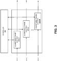
- FIG. 3 is a block diagram illustrating an example implementation in which controller 300 dithers quantized phase shifters 250-1 to 250-N of a phased array antenna.
- controller 300 may cause phase shifters 250-1 to 250-N to rapidly cycle between their states based on a desired phase shift.
- FIG. 3 will be described in conjunction with FIG. 4 , which is a flow diagram illustrating an example method 400 of dithering the states of quantized phase shifters in a phased array antenna to reduce quantization errors and side lobe levels in the phased array antenna.
- input signals are received at quantized phase shifters 250-1 to 250-N.
- individual instances of the same RF signal may be delivered to a respective quantized phase shifter 250-1 configured to generate a respective phase delay.
- the states of each quantized phase shifter 250-1 to 250-N is dithered using controller 300 to generate a time-averaged phase shifted signal.
- the state of each quantized phase shifter may be dithered by switching or cycling between the states of the quantized phase shifter at a frequency greater than the highest symbol rate of an adjacent satellite.
- switching may occur at a frequency of at least four times the highest symbol rate of the adjacent satellite. For example, if an adjacent Ku satellite operates using 40 MHz transponders, switching may occur at a rate of 160 MHz or greater.
- the phase shifted signals are output to respective antenna element circuits.
- Digital dithering of a phase shifter's state may be implemented using a variety of algorithms that cycle through the phase shifter states given a desired phase shift. For example, linear interpolation, the use of accumulator interpolation, or other types of algorithms may be implemented.
- the quantized phase may be used to create a power radiation pattern using a signal with a bandwidth that is much higher than that of the neighboring satellite.
- a group of patterns, which are produced from individual cycles, may then be averaged to produce a compliant radiation pattern.
- the number of cycles may be chosen such that the side lobes produced by the phased array antenna are sufficiently suppressed to a given level (e.g., in dBi).
- controller 300 may be embedded in a chip that has a plurality of switches for controlling the states of quantized phase shifters 250-1 to 250-N.
- controller 300 may be implemented as a complimentary metal-oxide-semiconductor (CMOS) controller on a chip comprising silicon-germanium switches.
- CMOS complimentary metal-oxide-semiconductor
- a chip including the quantized phase shifters may be embedded with an algorithm that may be used to dither the states of the quantized phase shifters.
- FIG. 5 is a block diagram illustrating an example digital dithering algorithm that may be applied to a 2-bit phase shifter in accordance with embodiments.
- the algorithm includes a subtractor 510, an integrator 520 including an adder 525 and digital sample delay module 527, a phase unwrapping module 530, and a quantizer 540 (2-bits in this example).
- the output phase Q out that is a result of quantization with a limited number of bits (2 bits in this example) is compared to a required phase Q req that is exact. An error is produced as a result of this comparison. This error is then provided as an input to integrator 520.
- the output phase is unwrapped using unwrapping module 530 to fall within the range of the quantized phase, that is [0°, 360°).
- the output is then quantized by quantizer 540 based on the number of bits specified by the quantizer.
- the loop cycle shown in FIG. 5 may be performed multiple times (e.g., two times, four times, ten times, etc.) and the radiated power of all the cycles is averaged to produce a dithered power radiation pattern.
- the signals transmitted over individual cycles are transmitted over a bandwidth that is much wider (e.g., at least four times) than the measurable bandwidth of the neighboring satellite.
- the resultant averaged, or dithered, power radiation pattern may be compliant with FCC 25.209.
- FIG. 6A shows experimental results illustrating the time-averaged directivity pattern (i.e., antenna gain in dBi as a function of scan angle) of a beam transmitted at 30 GHz using a phased array antenna that dithers 2-bit phase shifters.
- the 2-bit phase shifters were dithered using the digital dithering algorithm illustrated in FIG. 5 .
- FIG. 6B illustrates the directivity pattern when there is no dithering (one clock cycle).
- FIG. 6A illustrates the directivity pattern when there is dithering for ten clock cycles.
- the averaged array directivity pattern 610 after ten cycles has substantially reduced side lobes and is on par with earth station antenna performance standards as prescribed by FCC Rule 25.209.
- the max average directivity power in the main lobe is over 44 dBi.
- FIG. 7 illustrates a computer system 1000 upon which example embodiments according to the present disclosure can be implemented.
- Computer system 1000 can include a bus 1002 or other communication mechanism for communicating information, and a processor 1004 coupled to bus 1002 for processing information.
- Computer system 1000 may also include main memory 1006, such as a random access memory (RAM) or other dynamic storage device, coupled to bus 1002 for storing information and instructions to be executed by processor 1004.
- Main memory 1006 can also be used for storing temporary variables or other intermediate information during execution of instructions to be executed by processor 1004.
- Computer system 1000 may further include a read only memory (ROM) 1008 or other static storage device coupled to bus 1002 for storing static information and instructions for processor 1004.
- ROM read only memory
- a storage device 1010 such as a magnetic disk or optical disk, may additionally be coupled to bus 1002 for storing information and instructions.
- Computer system 1000 can be coupled via bus 1002 to a display 1012, such as a cathode ray tube (CRT), liquid crystal display (LCD), active matrix display, light emitting diode (LED)/organic LED (OLED) display, digital light processing (DLP) display, or plasma display, for displaying information to a computer user.
- a display 1012 such as a cathode ray tube (CRT), liquid crystal display (LCD), active matrix display, light emitting diode (LED)/organic LED (OLED) display, digital light processing (DLP) display, or plasma display
- An input device 1014 such as a keyboard including alphanumeric and other keys, may be coupled to bus 1002 for communicating information and command selections to processor 1004.
- cursor control 1016 such as a mouse, a trackball, or cursor direction keys for communicating direction information and command selections to processor 1004 and for controlling cursor movement on display 1012.
- dithering of the quantized phase shifter is provided by computer system 1000 in response to processor 1004 executing an arrangement of instructions contained in main memory 1006.
- Such instructions can be read into main memory 1006 from another computer-readable medium, such as storage device 1010.
- Execution of the arrangement of instructions contained in main memory 1006 causes processor 1004 to perform one or more processes described herein.
- processors in a multi-processing arrangement may also be employed to execute the instructions contained in main memory 1006.
- hard-wired circuitry is used in place of or in combination with software instructions to implement various embodiments.
- embodiments described in the present disclosure are not limited to any specific combination of hardware circuitry and software.
- Computer system 1000 may also include a communication interface 1018 coupled to bus 1002.
- Communication interface 1018 can provide a two-way data communication coupling to a network link 1020 connected to a local network 1022.
- communication interface 1018 may be a digital subscriber line (DSL) card or modem, an integrated services digital network (ISDN) card, a cable modem, or a telephone modem to provide a data communication connection to a corresponding type of telephone line.
- communication interface 1018 may be a local area network (LAN) card (e.g. for EthernetTM or an Asynchronous Transfer Model (ATM) network) to provide a data communication connection to a compatible LAN.
- LAN local area network
- Wireless links can also be implemented.
- communication interface 1018 sends and receives electrical, electromagnetic, or optical signals that carry digital data streams representing various types of information.
- communication interface 1018 may include peripheral interface devices, such as a Universal Serial Bus (USB) interface, a PCMCIA (Personal Computer Memory Card International Association) interface, etc.
- USB Universal Serial Bus
- PCMCIA Personal Computer Memory Card International Association
- Network link 1020 typically provides data communication through one or more networks to other data devices.
- network link 1020 can provide a connection through local network 1022 to a host computer 1024, which has connectivity to a network 1026 (e.g. a wide area network (WAN) or the global packet data communication network now commonly referred to as the "Internet") or to data equipment operated by service provider.
- a network 1026 e.g. a wide area network (WAN) or the global packet data communication network now commonly referred to as the "Internet”
- Local network 1022 and network 1026 may both use electrical, electromagnetic, or optical signals to convey information and instructions.
- the signals through the various networks and the signals on network link 1020 and through communication interface 1018, which communicate digital data with computer system 1000, are example forms of carrier waves bearing the information and instructions.
- Computer system 1000 may send messages and receive data, including program code, through the network(s), network link 1020, and communication interface 1018.
- a server (not shown) might transmit requested code belonging to an application program for implementing an embodiment of the present disclosure through network 1026, local network 1022 and communication interface 1018.
- Processor 1004 executes the transmitted code while being received and/or store the code in storage device 1010, or other non-volatile storage for later execution. In this manner, computer system 1000 obtains application code in the form of a carrier wave.
- Non-volatile media include, for example, optical or magnetic disks, such as storage device 1010.
- Volatile media may include dynamic memory, such as main memory 1006.
- Transmission media may include coaxial cables, copper wire and fiber optics, including the wires that comprise bus 1002. Transmission media can also take the form of acoustic, optical, or electromagnetic waves, such as those generated during radio frequency (RF) and infrared (IR) data communications.
- RF radio frequency
- IR infrared
- Computer-readable media include, for example, a floppy disk, a flexible disk, hard disk, magnetic tape, any other magnetic medium, a CD ROM, CDRW, DVD, any other optical medium, punch cards, paper tape, optical mark sheets, any other physical medium with patterns of holes or other optically recognizable indicia, a RAM, a PROM, and EPROM, a FLASH EPROM, any other memory chip or cartridge, a carrier wave, or any other medium from which a computer can read.
- a floppy disk a flexible disk, hard disk, magnetic tape, any other magnetic medium, a CD ROM, CDRW, DVD, any other optical medium, punch cards, paper tape, optical mark sheets, any other physical medium with patterns of holes or other optically recognizable indicia, a RAM, a PROM, and EPROM, a FLASH EPROM, any other memory chip or cartridge, a carrier wave, or any other medium from which a computer can read.
- Various forms of computer-readable media may be involved in providing instructions to a processor for execution.
- the instructions for carrying out at least part of the present disclosure may initially be borne on a magnetic disk of a remote computer.
- the remote computer loads the instructions into main memory and sends the instructions over a telephone line using a modem.
- a modem of a local computer system receives the data on the telephone line and uses an infrared transmitter to convert the data to an infrared signal and transmit the infrared signal to a portable computing device, such as a personal digital assistance (PDA) and a laptop.
- PDA personal digital assistance
- An infrared detector on the portable computing device receives the information and instructions borne by the infrared signal and places the data on a bus.
- the bus conveys the data to main memory, from which a processor retrieves and executes the instructions.
- the instructions received by main memory may optionally be stored on storage device either before or after execution by processor.
- FIG. 8 illustrates a chip set 1100 in which embodiments of the disclosure may be implemented.
- Chip set 1100 can include, for instance, processor and memory components described with respect to FIG. 8 incorporated in one or more physical packages.
- a physical package includes an arrangement of one or more materials, components, and/or wires on a structural assembly (e.g., a baseboard) to provide one or more characteristics such as physical strength, conservation of size, and/or limitation of electrical interaction.
- chip set 1100 includes a communication mechanism such as a bus 1002 for passing information among the components of the chip set 1100.
- a processor 1104 has connectivity to bus 1102 to execute instructions and process information stored in a memory 1106.
- Processor 1104 includes one or more processing cores with each core configured to perform independently.
- a multi-core processor enables multiprocessing within a single physical package. Examples of a multi-core processor include two, four, eight, or greater numbers of processing cores.
- processor 1104 includes one or more microprocessors configured in tandem via bus 1102 to enable independent execution of instructions, pipelining, and multithreading.
- Processor 1004 may also be accompanied with one or more specialized components to perform certain processing functions and tasks such as one or more digital signal processors (DSP) 1108, and/or one or more application-specific integrated circuits (ASIC) 1110.
- DSP 1108 can typically be configured to process real-world signals (e.g., sound) in real time independently of processor 1104.
- ASIC 1110 can be configured to performed specialized functions not easily performed by a general purposed processor.
- Other specialized components to aid in performing the inventive functions described herein include one or more field programmable gate arrays (FPGA) (not shown), one or more controllers (not shown), or one or more other special-purpose computer chips.
- FPGA field programmable gate arrays
- Memory 1106 includes both dynamic memory (e.g., RAM) and static memory (e.g., ROM) for storing executable instructions that, when executed by processor 1104, DSP 1108, and/or ASIC 1110, perform the process of example embodiments as described herein. Memory 1106 also stores the data associated with or generated by the execution of the process.
- dynamic memory e.g., RAM
- static memory e.g., ROM
- module might describe a given unit of functionality that can be performed in accordance with one or more embodiments of the present application.
- a module might be implemented utilizing any form of hardware, software, or a combination thereof.
- processors, controllers, ASICs, PLAs, PALs, CPLDs, FPGAs, logical components, software routines or other mechanisms might be implemented to make up a module.
- the various modules described herein might be implemented as discrete modules or the functions and features described can be shared in part or in total among one or more modules.
- module does not imply that the components or functionality described or claimed as part of the module are all configured in a common package. Indeed, any or all of the various components of a module, whether control logic or other components, can be combined in a single package or separately maintained and can further be distributed in multiple groupings or packages or across multiple locations.
Landscapes
- Engineering & Computer Science (AREA)
- Computer Networks & Wireless Communication (AREA)
- Signal Processing (AREA)
- Physics & Mathematics (AREA)
- Astronomy & Astrophysics (AREA)
- Aviation & Aerospace Engineering (AREA)
- General Physics & Mathematics (AREA)
- Variable-Direction Aerials And Aerial Arrays (AREA)
- Radio Transmission System (AREA)
Description
- The present disclosure relates generally to phased array antennas. More particularly, some embodiments of the present disclosure are directed toward systems and methods for using digital dithering for reduction of quantization errors and side-lobe levels in phased array antennas.
- Phased array antennas include multiple transmitting and/or receiving antenna elements that can be used together to form a directional radiation pattern. The relative phases or the respective signals feeding the antennas are controlled to create an effective radiation pattern that is strongest in a desired direction and suppressed in undesired directions. In this manner the antenna beam may be rapidly steered without any mechanical steering of the antenna (e.g., using a gimbal).
- When quantized phase shifters are used to control the phases of the signals feeding the antenna elements, quantization errors result from the finite number of digitalization bits available to represent a signal phase. For example, in the case of a 2-bit phase shifter with four states, 0°, 90°, 180°, and 270°, the step size is 90° and the maximum quantization error is ±45°. When a radiating element requires a phase of 46°, the nearest state of this phase shifter is 90°, for which the error (between desired and actual) is 44°.
- Quantization errors degrade antenna performance by increasing side lobe levels (SLL), i.e. the power density of side lobes that represent unwanted radiation in unwanted directions. Using a phase shifter with a greater number of quantization bits may improve antenna efficiency and lower SLLs, but it comes at the cost of a more expensive and complex phase shifter and control circuit.
- H. Kamoda et al. in "Reduction in quantization lobes due to digital phase shifters for phased array radars" Microwave Conference Proceedings (APMC) 2011 p1618-1621, discloses a method to reduce quantization lobes for phased array antennas with lower-bit phase shifters. The transmission and reception of a radar signal are repeated N time while changing the phase quantization error for each antenna element by changing a phase offset that is added to the ideal phase shifts for all antennas before the quantization for each antenna element is performed. The N received signals are then integrated coherently by subtracting the phase offset that each signal has undergone in passing through the phased array antenna. The integrated signal is equivalent to one received by an antenna with reduced side-lobes.
-
US6266010B1 discloses an antenna system for transmitting and receiving signals in communication systems and radar applications. The antenna system uses electronic beam forming to mathematically synthesize the signals desired for object detection and tracking. Rather than using passive waveguide material having multiple antenna system ports that must be individually processed in separate transceiver channels, the antenna ports are coupled to a beam forming network of the antenna system. The beam forming network includes a single port that can be coupled to a single transceiver channel. The beam forming network is configured to mathematically synthesize each of the desired signals needed by the transceiver to calculate desired information, such as the azimuth and elevation of an object to be detected and/or tracked (for example, the summed output signal and a difference output signal). The beam forming network can be configured to sequentially produce each of the desired signals. -
US5103232A discloses a means of decorrelating phase quantization errors in a phased array radar antenna using digital randomization at each of the array elements to reduce peak steering errors and to reduce peak side-lobe levels of the antenna. A random phase adjust term is provided to each of the array's antenna elements which comprises a distributed controller co-located with a digital phase shifter. The distributed controllers are each programmed with a random phase adjust term which represents a phase shift adjustment statistically independent from element to element. -
US9379436B1 - Systems and methods disclosed herein provide techniques for reducing quantization errors and side lobe levels in phased array antennas.
- In a first aspect of the invention, there is provided a method as defined in claim 1. Preferred and/or optional features are set out in the dependent claims. In some implementations the quantized phase shifter may be a 1-bit or 2-bit phase shifter.
- In a second aspect of the invention, there is provided a phase array antenna includes: a plurality of quantized phase shifters; a controller configured to perform the method of the first aspect; and a plurality of antenna elements, where each of the plurality of antenna elements is configured to receive a time-averaged, phase shifted signal from a respective one of the plurality of quantized phase shifters. The phased array antenna may be a phased array antenna of a very small aperture terminal (VSAT). The phased array antenna may also be a phased array antenna of a satellite.
- The techniques disclosed herein may be implemented in a phased array antenna receiver. Accordingly, in a third aspect of the invention, there is provided a method as defined in claim 11. Preferred and/or optional features are set out in the dependent claims. In an implementation, the method further comprises: amplifying the RF communication signal received at each of the plurality of antenna elements using a low noise amplifier.
- Other features and aspects of the disclosure will become apparent from the following detailed description, taken in conjunction with the accompanying drawings, which illustrate, by way of example, the features in accordance with various embodiments. The summary is not intended to limit the scope of the invention, which is defined solely by the claims attached hereto.
- The technology disclosed herein, in accordance with one or more various embodiments, is described in detail with reference to the following figures. The drawings are provided for purposes of illustration only and merely depict typical or example embodiments of the disclosed technology. These drawings are provided to facilitate the reader's understanding of the disclosed technology and shall not be considered limiting of the breadth, scope, or applicability thereof. It should be noted that for clarity and ease of illustration these drawings are not necessarily made to scale.
-
FIG. 1 is a block diagram illustrating an example bi-directional phased array antenna in which embodiments may be implemented. -
FIG. 2 illustrates one particular implementation of a phased array antenna whereby elements are arranged in a circular array and are spaced apart in half wavelengths. -
FIG. 3 is a block diagram illustrating an example implementation in which controller dithers quantized phase shifters of a phased array antenna. -
FIG. 4 is a flow diagram illustrating an example method of dithering the states of quantized phase shifters in a phased array antenna to reduce quantization errors and side lobe levels in the phased array antenna. -
FIG. 5 is a diagram illustrating an example digital dithering algorithm that may be applied to a 2-bit phase shifter in accordance with embodiments. -
FIGs. 6A depicts experimental results illustrating the time-averaged directivity pattern of a beam transmitted at 30 GHz using a phased array antenna that dithers 2-bit phase shifters. -
FIGs. 6B depicts experimental results illustrating the time-averaged directivity pattern of a beam transmitted at 30 GHz using a phased array antenna that does not dither. -
FIG. 7 illustrates an example computing module that may be used in implementing features of various embodiments. -
FIG. 8 illustrates an example chip set that can be utilized in implementing architectures and methods for digital dithering for reduction of quantization errors and side-lobe levels in phased array antennas in accordance with various embodiments. - The figures are not intended to be exhaustive or to limit the invention to the precise form disclosed. It should be understood that the invention can be practiced with modification and alteration, and that the disclosed technology be limited only by the claims.
- As alluded to above, conventional phased array antennas that utilize quantized phase shifters rely on high bit phase shifters to minimize quantization errors. However, this increases the cost of the antenna in a number of areas: (1) the phase shifter devices themselves (costs approximately proportional to the number of bits), (2) the control circuitry, as its complexity increases with the number of phase shifting bits; (3) the transmission lines, typically waveguides or Printed Circuit Boards (PCB), as they become more complex with the number of phase shifting bits.
- Embodiments of the systems and methods disclosed herein provide techniques for addressing the aforementioned problems by dithering the state of the quantized phase shifter to achieve a time-average value that significantly reduces quantization errors of the quantized phase shifter. By rapidly switching between the different states of the quantized phase shifter, a time-average value close to a desired phase state may be achieved even with a low resolution (e.g., 1-bit or 2-bit) phase shifter. This method may provide a number of advantages over conventional approaches of using phase shifters with higher bit-counts. First, this method reduces the quantization error and reduces antenna SLL, all at no additional hardware cost. Second, this method negates the requirement for calibration that is typical in phase shifter hardware implementations of any number of bits, but particularly high number of bits. This results in significant cost savings as calibration is quite time consuming, requires precision measurement instruments, and typically represents a significant percentage of system costs.
-
FIG. 1 is a block diagram illustrating an example bi-directional phasedarray antenna 100, including antenna elements 150, in which embodiments may be implemented. Although a bi-directional phasedarray antenna 100 is shown in this example, the methods disclosed herein may implemented in unidirectional transmit phased array antennas. Phased array antenna may be implemented as a dynamic phased array antenna (i.e., each antenna element or group of elements may have an adjustable phase shifter), an active phased array antenna (i.e., each antenna element or group elements may have transmit amplification circuitry), a passive phased array antenna, or some variant thereof. -
Phased array antenna 100 may be implemented in a variety of devices. For example, in one implementation phasedarray antenna 100 may be implemented in a fixed terminal (e.g., a VSAT terminal) communicating with a satellite. In such implementations, the technology disclosed herein may offer an affordable way of steering the antenna beam, automatically pointing the beam to the satellite, and periodically repointing the antenna beam to compensate for minor antenna movements due to ground settlement, ground freezing/thawing cycles, etc. In other implementations, phasedarray antenna 100 may be implemented in moving satellites (e.g., a low earth orbit satellite, a medium earth orbit satellite, etc.) and/or moving terminals that are on moving platforms (e.g., on a terrestrial vehicle or aircraft). In such implementations, the technology disclosed herein may provide an affordable way of fast beam tracking that constantly points the antenna beam towards the satellite. - As illustrated by
FIG. 1 , example phasedarray antenna 100 includes apower divider 120, transmitamplifiers 130, antenna elements 150, one or morelow noise amplifiers 140,power combiner 160, dithered and quantizedphase shifter module 200, andcontroller 300. It should be noted that one of ordinary skill in the art will understand how other transmit or receive configurations can be implemented in phasedarray antenna 100, and that certain components of phasedarray antenna 100 may be implemented in either digital form (e.g., as software running on a DSP or other processing device, with the addition of a DAC) or as analog components. Additionally, although the components of phasedarray antenna 100 are shown in a particular order in this example, one of ordinary skill in the art reading this description will understand that the order of components can be varied and some components may be excluded. For simplicity, a discussion of the receive operation of phasedarray antenna 100, and receive components such asLNAs 140,power combiner 160, andreceiver 170 will be omitted. However, one having skill in the art will appreciate how such components may implement the reverse operation of the transmit components described herein. - During transmit operation, illustrated by
FIG. 1 , phasedarray antenna 100 may steer anantenna beam 400 in a direction by varying the phases of radiating antenna elements 150 so as to produce an effective radiation pattern (as determined by constructive and destructive interference of the signals emitted by each antenna element 150) in a desired direction (azimuthal and/or elevation). For example, the phase of every radiating antenna element 150 may be varied such that there is progressive phase along the rows and/or columns of the radiating elements. As further described below, this may be implemented by using a phase shifter (for every radiating element or group of elements) that can vary the phase of the RF energy radiated by the respective element. As illustrated in this example, abeam 400 is steered at an angle θ relative to elements 150 and includes amain lobe 410 andside lobes 420A-420B. - With specific reference to the elements of phased
array antenna 100 during a transmit operation, phasedarray antenna 100 receives an RF signal from anRF source 110. For example,RF source 110 may take a bit source as an input and perform functions such as signal encoding, interleaving, modulation, and filtering. Signals coming fromRF source 110 may be based, for example, on the DVB-S2 standard (ETSI EN 302 307) using signal constellations up to and including at least 32-APSK, or on the Internet Protocol over Satellite (IPoS) standard (ETSI TS 102 354), or on other standard or proprietary specifications incorporating adaptive coding and modulation. Other suitable signal types may also be used, including, for example higher data rate variations of DVB-S2, or DVB-S2 extensions or adaptations sometimes designated as DVB-S2X. - Additionally,
RF source 110 may modulate an information signal onto a suitable carrier (e.g., an RF carrier signal) at a desired frequency. For example, phasedarray antenna 100 may operate in the Ka-band, Ku-band, C-band or other suitable band. However, it should be noted that the up conversion or modulation of the signal onto a suitable carrier may be performed before or after the phase delay. -
Power divider 120 may couple a defined amount of power of a signal provided byRF source 110 to a plurality of signal paths, each of the divided signals being fed along a path to an antenna element 150. For instance, in implementations where each antenna element 150 includes a respective phase shifter,power divider 120 may feed a respective instance of a signal to the phase shifter, which is phase shifted at a quantized phase shifter ofmodule 200, amplified byamplifier 130 and transmitted by an antenna element 150. - Depending on the implementation, antenna elements 150 may be arranged in a variety of configurations. For example, antenna elements 150 may be linearly arranged in a linear array, in a rectangular array, a circular array, or some other suitable arrangement. Within the arrangement, antenna elements 150 may be spaced apart depending on the wavelength of the transmitted waveform. For example, elements 150 may be spaced apart in half wavelengths or quarter wavelengths. The number of antenna elements 150 may depend on the gain requirements of phased
array antenna 100 and the type of radiator used for each antenna element. For example, a 20 dB gain antenna may require about 100 elements or more, a 30 dB gain antenna may require about 1000 elements or more, and a 40 dB antenna may require about 10,000 elements or more, and so forth.FIG. 2 illustrates one particular implementation of a phased array antenna whereby elements 150 are arranged in a circular array and are spaced apart in half wavelengths. - Dithered and quantized
phase shifter module 200, may include a quantized phase shifter for each element 150 or group of elements 150 that changes the transmission phase angle or true time delay of a signal transmitted by a respective element 150. Each quantized phase shifter is digitally controlled using one or more bits (e.g., 1 bit, 2 bits, 3 bits, etc.), which provide a discrete set of states that are controlled using acontroller 300. For example, as discussed above, a two bit phase shifter may have four states: 0°, 90°, 180°, and 270°. As another example, a three bit phase shifter may include eight states: 0°, 45°, 90°, 135°, 180°, 225°, 270°, and 315°. In some implementations, the quantized phase shifters may provide a true time delay as opposed to a constant phase shift over a frequency. For ease of discussion, as used herein, the term "quantized phase shifter" refers to either a phase shifter that provides a constant phase shift over a frequency or a true time delay. Similarly, the term "n-bit phase shifter" may refer to either variety of phase shifter that can be controlled using n digital bits. - During operation, further described below,
controller 300 may cause each quantized phase shifter to rapidly switch between each of its states (e.g., using pulse width modulation), thereby effectively dithering the output of the phase shifter and reducing quantization error. For example, consider the case of a 2-bit phase shifter (includingstates 0° and 90°) and desired phase angle of 22.5 for an antenna element 150. By rapidly switching between the 0° and 90° states with a 75% duty cycle in the 0° state and a 25% duty cycle in the 90° state (e.g., three 0° states for every one 90° state), the time-averaged value of the state of the quantized phase shifter is 22.5°, thereby effectively reducing the quantization error to 0° and providing the same resolution as a 4-bit phase shifter. This in turn may reduce side lobe degradation of the directional beam transmitted by the phased array antenna. As another example, consider the case of a 2-bit phase shifter (including states of 1 µs and 2 µs) and desired true time delay of 1.5 µs for an antenna element 150. By rapidly switching between the 1 µs and 2 µs states at the same duty cycle, the time-averaged value of the state of the quantized phase shifter is 1.5 µs. -
FIG. 3 is a block diagram illustrating an example implementation in whichcontroller 300 dithers quantized phase shifters 250-1 to 250-N of a phased array antenna. In this example,controller 300 may cause phase shifters 250-1 to 250-N to rapidly cycle between their states based on a desired phase shift.FIG. 3 will be described in conjunction withFIG. 4 , which is a flow diagram illustrating anexample method 400 of dithering the states of quantized phase shifters in a phased array antenna to reduce quantization errors and side lobe levels in the phased array antenna. - At
operation 410, input signals are received at quantized phase shifters 250-1 to 250-N. For example, individual instances of the same RF signal may be delivered to a respective quantized phase shifter 250-1 configured to generate a respective phase delay. - At
operation 420, the states of each quantized phase shifter 250-1 to 250-N is dithered usingcontroller 300 to generate a time-averaged phase shifted signal. In various implementations, the state of each quantized phase shifter may be dithered by switching or cycling between the states of the quantized phase shifter at a frequency greater than the highest symbol rate of an adjacent satellite. In particular implementations, switching may occur at a frequency of at least four times the highest symbol rate of the adjacent satellite. For example, if an adjacent Ku satellite operates using 40 MHz transponders, switching may occur at a rate of 160 MHz or greater. Atoperation 430, the phase shifted signals are output to respective antenna element circuits. - Digital dithering of a phase shifter's state may be implemented using a variety of algorithms that cycle through the phase shifter states given a desired phase shift. For example, linear interpolation, the use of accumulator interpolation, or other types of algorithms may be implemented. During each cycle, the quantized phase may be used to create a power radiation pattern using a signal with a bandwidth that is much higher than that of the neighboring satellite. A group of patterns, which are produced from individual cycles, may then be averaged to produce a compliant radiation pattern. In implementations, the number of cycles may be chosen such that the side lobes produced by the phased array antenna are sufficiently suppressed to a given level (e.g., in dBi).
- In implementations,
controller 300 may be embedded in a chip that has a plurality of switches for controlling the states of quantized phase shifters 250-1 to 250-N. For example,controller 300 may be implemented as a complimentary metal-oxide-semiconductor (CMOS) controller on a chip comprising silicon-germanium switches. In implementations, a chip including the quantized phase shifters, may be embedded with an algorithm that may be used to dither the states of the quantized phase shifters. -
FIG. 5 is a block diagram illustrating an example digital dithering algorithm that may be applied to a 2-bit phase shifter in accordance with embodiments. As illustrated, the algorithm includes asubtractor 510, anintegrator 520 including anadder 525 and digitalsample delay module 527, aphase unwrapping module 530, and a quantizer 540 (2-bits in this example). - As illustrated by
FIG. 5 , the output phase Qout that is a result of quantization with a limited number of bits (2 bits in this example) is compared to a required phase Qreq that is exact. An error is produced as a result of this comparison. This error is then provided as an input tointegrator 520. The output phase is unwrapped usingunwrapping module 530 to fall within the range of the quantized phase, that is [0°, 360°). The output is then quantized byquantizer 540 based on the number of bits specified by the quantizer. - The loop cycle shown in
FIG. 5 may be performed multiple times (e.g., two times, four times, ten times, etc.) and the radiated power of all the cycles is averaged to produce a dithered power radiation pattern. In implementations, the signals transmitted over individual cycles are transmitted over a bandwidth that is much wider (e.g., at least four times) than the measurable bandwidth of the neighboring satellite. The resultant averaged, or dithered, power radiation pattern may be compliant with FCC 25.209. -
FIG. 6A shows experimental results illustrating the time-averaged directivity pattern (i.e., antenna gain in dBi as a function of scan angle) of a beam transmitted at 30 GHz using a phased array antenna that dithers 2-bit phase shifters. In the examples ofFIGs. 6A , the 2-bit phase shifters were dithered using the digital dithering algorithm illustrated inFIG. 5 .FIG. 6B illustrates the directivity pattern when there is no dithering (one clock cycle).FIG. 6A illustrates the directivity pattern when there is dithering for ten clock cycles. The averagedarray directivity pattern 610 after ten cycles has substantially reduced side lobes and is on par with earth station antenna performance standards as prescribed by FCC Rule 25.209. The max average directivity power in the main lobe (scan angle of 0°) is over 44 dBi. -
FIG. 7 illustrates acomputer system 1000 upon which example embodiments according to the present disclosure can be implemented.Computer system 1000 can include a bus 1002 or other communication mechanism for communicating information, and aprocessor 1004 coupled to bus 1002 for processing information.Computer system 1000 may also includemain memory 1006, such as a random access memory (RAM) or other dynamic storage device, coupled to bus 1002 for storing information and instructions to be executed byprocessor 1004.Main memory 1006 can also be used for storing temporary variables or other intermediate information during execution of instructions to be executed byprocessor 1004.Computer system 1000 may further include a read only memory (ROM) 1008 or other static storage device coupled to bus 1002 for storing static information and instructions forprocessor 1004. Astorage device 1010, such as a magnetic disk or optical disk, may additionally be coupled to bus 1002 for storing information and instructions. -
Computer system 1000 can be coupled via bus 1002 to adisplay 1012, such as a cathode ray tube (CRT), liquid crystal display (LCD), active matrix display, light emitting diode (LED)/organic LED (OLED) display, digital light processing (DLP) display, or plasma display, for displaying information to a computer user. Aninput device 1014, such as a keyboard including alphanumeric and other keys, may be coupled to bus 1002 for communicating information and command selections toprocessor 1004. Another type of user input device iscursor control 1016, such as a mouse, a trackball, or cursor direction keys for communicating direction information and command selections toprocessor 1004 and for controlling cursor movement ondisplay 1012. - According to one embodiment of the disclosure, dithering of the quantized phase shifter, in accordance with example embodiments, is provided by
computer system 1000 in response toprocessor 1004 executing an arrangement of instructions contained inmain memory 1006. Such instructions can be read intomain memory 1006 from another computer-readable medium, such asstorage device 1010. Execution of the arrangement of instructions contained inmain memory 1006 causesprocessor 1004 to perform one or more processes described herein. One or more processors in a multi-processing arrangement may also be employed to execute the instructions contained inmain memory 1006. In alternative embodiments, hard-wired circuitry is used in place of or in combination with software instructions to implement various embodiments. Thus, embodiments described in the present disclosure are not limited to any specific combination of hardware circuitry and software. -
Computer system 1000 may also include acommunication interface 1018 coupled to bus 1002.Communication interface 1018 can provide a two-way data communication coupling to anetwork link 1020 connected to alocal network 1022. By way of example,communication interface 1018 may be a digital subscriber line (DSL) card or modem, an integrated services digital network (ISDN) card, a cable modem, or a telephone modem to provide a data communication connection to a corresponding type of telephone line. As another example,communication interface 1018 may be a local area network (LAN) card (e.g. for Ethernet™ or an Asynchronous Transfer Model (ATM) network) to provide a data communication connection to a compatible LAN. Wireless links can also be implemented. In any such implementation,communication interface 1018 sends and receives electrical, electromagnetic, or optical signals that carry digital data streams representing various types of information. Further,communication interface 1018 may include peripheral interface devices, such as a Universal Serial Bus (USB) interface, a PCMCIA (Personal Computer Memory Card International Association) interface, etc. -
Network link 1020 typically provides data communication through one or more networks to other data devices. By way of example,network link 1020 can provide a connection throughlocal network 1022 to ahost computer 1024, which has connectivity to a network 1026 (e.g. a wide area network (WAN) or the global packet data communication network now commonly referred to as the "Internet") or to data equipment operated by service provider.Local network 1022 andnetwork 1026 may both use electrical, electromagnetic, or optical signals to convey information and instructions. The signals through the various networks and the signals onnetwork link 1020 and throughcommunication interface 1018, which communicate digital data withcomputer system 1000, are example forms of carrier waves bearing the information and instructions. -
Computer system 1000 may send messages and receive data, including program code, through the network(s),network link 1020, andcommunication interface 1018. In the Internet example, a server (not shown) might transmit requested code belonging to an application program for implementing an embodiment of the present disclosure throughnetwork 1026,local network 1022 andcommunication interface 1018.Processor 1004 executes the transmitted code while being received and/or store the code instorage device 1010, or other non-volatile storage for later execution. In this manner,computer system 1000 obtains application code in the form of a carrier wave. - The term "computer-readable medium" as used herein refers to any medium that participates in providing instructions to
processor 1004 for execution. Such a medium may take many forms, including but not limited to non-volatile media, volatile media, and transmission media. Non-volatile media include, for example, optical or magnetic disks, such asstorage device 1010. Volatile media may include dynamic memory, such asmain memory 1006. Transmission media may include coaxial cables, copper wire and fiber optics, including the wires that comprise bus 1002. Transmission media can also take the form of acoustic, optical, or electromagnetic waves, such as those generated during radio frequency (RF) and infrared (IR) data communications. Common forms of computer-readable media include, for example, a floppy disk, a flexible disk, hard disk, magnetic tape, any other magnetic medium, a CD ROM, CDRW, DVD, any other optical medium, punch cards, paper tape, optical mark sheets, any other physical medium with patterns of holes or other optically recognizable indicia, a RAM, a PROM, and EPROM, a FLASH EPROM, any other memory chip or cartridge, a carrier wave, or any other medium from which a computer can read. - Various forms of computer-readable media may be involved in providing instructions to a processor for execution. By way of example, the instructions for carrying out at least part of the present disclosure may initially be borne on a magnetic disk of a remote computer. In such a scenario, the remote computer loads the instructions into main memory and sends the instructions over a telephone line using a modem. A modem of a local computer system receives the data on the telephone line and uses an infrared transmitter to convert the data to an infrared signal and transmit the infrared signal to a portable computing device, such as a personal digital assistance (PDA) and a laptop. An infrared detector on the portable computing device receives the information and instructions borne by the infrared signal and places the data on a bus. The bus conveys the data to main memory, from which a processor retrieves and executes the instructions. The instructions received by main memory may optionally be stored on storage device either before or after execution by processor.
-
FIG. 8 illustrates achip set 1100 in which embodiments of the disclosure may be implemented. Chip set 1100 can include, for instance, processor and memory components described with respect toFIG. 8 incorporated in one or more physical packages. By way of example, a physical package includes an arrangement of one or more materials, components, and/or wires on a structural assembly (e.g., a baseboard) to provide one or more characteristics such as physical strength, conservation of size, and/or limitation of electrical interaction. - In one embodiment, chip set 1100 includes a communication mechanism such as a bus 1002 for passing information among the components of the
chip set 1100. Aprocessor 1104 has connectivity to bus 1102 to execute instructions and process information stored in amemory 1106.Processor 1104 includes one or more processing cores with each core configured to perform independently. A multi-core processor enables multiprocessing within a single physical package. Examples of a multi-core processor include two, four, eight, or greater numbers of processing cores. Alternatively or in addition,processor 1104 includes one or more microprocessors configured in tandem via bus 1102 to enable independent execution of instructions, pipelining, and multithreading.Processor 1004 may also be accompanied with one or more specialized components to perform certain processing functions and tasks such as one or more digital signal processors (DSP) 1108, and/or one or more application-specific integrated circuits (ASIC) 1110.DSP 1108 can typically be configured to process real-world signals (e.g., sound) in real time independently ofprocessor 1104. Similarly,ASIC 1110 can be configured to performed specialized functions not easily performed by a general purposed processor. Other specialized components to aid in performing the inventive functions described herein include one or more field programmable gate arrays (FPGA) (not shown), one or more controllers (not shown), or one or more other special-purpose computer chips. -
Processor 1104 and accompanying components have connectivity to thememory 1106 via bus 1102.Memory 1106 includes both dynamic memory (e.g., RAM) and static memory (e.g., ROM) for storing executable instructions that, when executed byprocessor 1104,DSP 1108, and/orASIC 1110, perform the process of example embodiments as described herein.Memory 1106 also stores the data associated with or generated by the execution of the process. - As used herein, the term module might describe a given unit of functionality that can be performed in accordance with one or more embodiments of the present application. As used herein, a module might be implemented utilizing any form of hardware, software, or a combination thereof. For example, one or more processors, controllers, ASICs, PLAs, PALs, CPLDs, FPGAs, logical components, software routines or other mechanisms might be implemented to make up a module. In implementation, the various modules described herein might be implemented as discrete modules or the functions and features described can be shared in part or in total among one or more modules. In other words, as would be apparent to one of ordinary skill in the art after reading this description, the various features and functionality described herein may be implemented in any given application and can be implemented in one or more separate or shared modules in various combinations and permutations. Even though various features or elements of functionality may be individually described or claimed as separate modules, one of ordinary skill in the art will understand that these features and functionality can be shared among one or more common software and hardware elements, and such description shall not require or imply that separate hardware or software components are used to implement such features or functionality.
- Where components or modules of the application are implemented in whole or in part using software, in one embodiment, these software elements can be implemented to operate with a computing or processing module capable of carrying out the functionality described with respect thereto. One such example computing module is shown in
FIG. 7 . Various embodiments are described in terms of this example-computing module 1000. After reading this description, it will become apparent to a person skilled in the relevant art how to implement the application using other computing modules or architectures. - Although described above in terms of various exemplary embodiments and implementations, it should be understood that the various features, aspects and functionality described in one or more of the individual embodiments are not limited in their applicability to the particular embodiment with which they are described, but instead can be applied, alone or in various combinations, to one or more of the other embodiments of the present application, whether or not such embodiments are described and whether or not such features are presented as being a part of a described embodiment. Thus, the breadth and scope of the present application should not be limited by any of the above-described exemplary embodiments.
- Terms and phrases used in the present application, and variations thereof, unless otherwise expressly stated, should be construed as open ended as opposed to limiting. As examples of the foregoing: the term "including" should be read as meaning "including, without limitation" or the like; the term "example" is used to provide exemplary instances of the item in discussion, not an exhaustive or limiting list thereof; the terms "a" or "an" should be read as meaning "at least one," "one or more" or the like; and adjectives such as "conventional," "traditional," "normal," "standard," "known" and terms of similar meaning should not be construed as limiting the item described to a given time period or to an item available as of a given time, but instead should be read to encompass conventional, traditional, normal, or standard technologies that may be available or known now or at any time in the future. Likewise, where this document refers to technologies that would be apparent or known to one of ordinary skill in the art, such technologies encompass those apparent or known to the skilled artisan now or at any time in the future.
- The use of the term "module" does not imply that the components or functionality described or claimed as part of the module are all configured in a common package. Indeed, any or all of the various components of a module, whether control logic or other components, can be combined in a single package or separately maintained and can further be distributed in multiple groupings or packages or across multiple locations.
- Additionally, the various embodiments set forth herein are described in terms of exemplary block diagrams, flow charts and other illustrations. As will become apparent to one of ordinary skill in the art after reading this document, the illustrated embodiments and their various alternatives can be implemented without confinement to the illustrated examples. For example, block diagrams and their accompanying description should not be construed as mandating a particular architecture or configuration
Claims (13)
- A method (400), comprising:receiving (410) an input signal at a quantized phase shifter (250-1 to 250-N) of a phased array antenna (100);obtaining (420) a time averaged, phase shifted signal that reduces a quantization error of the phase shifter, wherein obtaining the time averaged signal comprises:switching between two phase states of the quantized phase shifter a plurality of times to obtain a plurality of phase shifted values; andapplying a linear interpolation or accumulator interpolation to the plurality of phase shifted values to obtain a time averaged value of a state of the quantized phase shifter that is between values of the two phase states; andoutputting (430) the time averaged, phase shifted signal to an antenna element (150) circuit of the phased array antenna.
- The method of claim 1, further comprising: receiving a signal from an adjacent satellite, said signal having a symbol rate, wherein the rate of switching between the two phase states is greater than the symbol rate of the adjacent satellite.
- The method of claim 2, wherein the rate of switching between the two phase states is at least four times greater than the symbol rate of the adjacent satellite.
- The method of claim 1 or any of claims 2 to 3, wherein obtaining (420) the time averaged, phase shifted signal comprises:obtaining an error signal by comparing an output phase of the time averaged, phase shifted signal to a required phase; andproviding the error signal as an input to an integrator (520) to obtain an integrated signal.
- The method of claim 4, wherein obtaining (420) the time averaged, phase shifted signal further comprises:unwrapping the output phase of the integrated signal to obtain an unwrapped signal; andquantizing the unwrapped signal.
- The method of claim 1 or any of claims 2 to 5, wherein the quantized phase shifter (250-1 to 250-N) is a 1-bit or 2-bit phase shifter.
- The method of claim 1 or any of claims 2 to 6, wherein the quantized phase shifter (250-1 to 250-N) is configured to provide:a true time delay of the input signal.
- A phased array antenna (100), comprising:a plurality of quantized phase shifters (250-1 to 250-N);a controller (300) configured to perform the method of any of claims 1 to 7; anda plurality of antenna elements (150), wherein each of the plurality of antenna elements is configured to receive the time-averaged, phase shifted signal from a respective one of the plurality of quantized phase shifters.
- The phased array antenna of claim 8, wherein each of the plurality of quantized phase shifters (250-1 to 250-N) is a 1-bit or 2-bit phase shifter.
- The phased array antenna of claim 8 or 9, wherein the phased array antenna (100) is:a phased array antenna of a very small aperture terminal, VSAT; ora phased array antenna of a satellite.
- A method, comprising:receiving an RF communication signal at each of a plurality of antenna elements (150) of a phased array antenna (100);outputting a signal from an antenna element to a quantized phase shifter; andobtaining a time averaged, phase shifted signal that reduces a quantization error of the phase shifter, wherein obtaining the time averaged signal comprises:switching between two phase states of the quantized phase shifter a plurality of times to obtain a plurality of phase shifted values; andapplying a linear interpolation or accumulator interpolation to the plurality of phase shifted values to obtain a time averaged value of a state of the quantized phase shifter that is between values of the two phase states.
- The method of claim 11:wherein obtaining the time averaged, phase shifted signal comprises: obtaining an error signal by comparing an output phase to a required phase; and providing the error signal as an input to an integrator to obtain an integrated signal; and/orfurther comprising amplifying the RF communication signal received at each of the plurality of antenna elements using a low noise amplifier.
- The method of claim 1, wherein switching between two phase states of the quantized phase shifter a plurality of times to obtain a plurality of phase shifted values comprises: using pulse width modulation duty cycles corresponding to the two phase states.
Applications Claiming Priority (2)
| Application Number | Priority Date | Filing Date | Title |
|---|---|---|---|
| US15/396,070 US10374663B2 (en) | 2016-12-30 | 2016-12-30 | Digital dithering for reduction of quantization errors and side-lobe levels in phased array antennas |
| PCT/US2017/068812 WO2018126068A1 (en) | 2016-12-30 | 2017-12-28 | Digital dithering for reduction of quantization errors and side-lobe levels in phased array antennas |
Publications (2)
| Publication Number | Publication Date |
|---|---|
| EP3563452A1 EP3563452A1 (en) | 2019-11-06 |
| EP3563452B1 true EP3563452B1 (en) | 2021-09-15 |
Family
ID=61074513
Family Applications (1)
| Application Number | Title | Priority Date | Filing Date |
|---|---|---|---|
| EP17835979.0A Active EP3563452B1 (en) | 2016-12-30 | 2017-12-28 | Digital dithering for reduction of quantization errors and side-lobe levels in phased array antennas |
Country Status (4)
| Country | Link |
|---|---|
| US (1) | US10374663B2 (en) |
| EP (1) | EP3563452B1 (en) |
| BR (1) | BR112019013594B1 (en) |
| WO (1) | WO2018126068A1 (en) |
Families Citing this family (13)
| Publication number | Priority date | Publication date | Assignee | Title |
|---|---|---|---|---|
| WO2011041754A1 (en) * | 2009-10-02 | 2011-04-07 | Research In Motion Limited | Mobility in a wireless network |
| US11038474B2 (en) | 2017-11-01 | 2021-06-15 | Analog Devices Global Unlimited Company | Phased array amplifier linearization |
| US10439707B1 (en) * | 2018-06-01 | 2019-10-08 | Rockwell Collins, Inc. | Systems and methods for mitigating adjacent satellite interference |
| WO2020218290A1 (en) * | 2019-04-25 | 2020-10-29 | 株式会社村田製作所 | Antenna module and communication device |
| CN110311740B (en) * | 2019-06-10 | 2021-08-31 | 北京信息科技大学 | A Phase Blur Detection and Correction Method Based on 1bit Quantization |
| JP7317599B2 (en) * | 2019-07-04 | 2023-07-31 | 株式会社東芝 | antenna device |
| CN110611169B (en) * | 2019-09-17 | 2021-04-02 | 上海交通大学 | Phased array antenna system based on periodic phase modulation and application method thereof |
| CN112928495B (en) * | 2021-01-21 | 2022-09-20 | 南京理工大学 | High-precision sequential phase-feeding method for K-bit digital phase shifter based on FPGA |
| CN113258293B (en) * | 2021-05-12 | 2023-06-16 | 哈尔滨工业大学(深圳) | Millimeter wave large-scale array beam forming system based on combined resolution phase shifter |
| JP7761315B2 (en) * | 2022-02-16 | 2025-10-28 | マサチューセッツ インスティテュート オブ テクノロジー | Terahertz beam steering antenna array |
| US12556272B2 (en) | 2022-12-12 | 2026-02-17 | Taara Connect, Inc. | Optical phased array wavefront sensing and control |
| US12619123B2 (en) | 2022-12-12 | 2026-05-05 | Taara Connect, Inc. | Optical phased array wavefront sensing and control |
| US20250373557A1 (en) * | 2024-06-03 | 2025-12-04 | Texas Instruments Incorporated | Dithering of recovered signal |
Family Cites Families (21)
| Publication number | Priority date | Publication date | Assignee | Title |
|---|---|---|---|---|
| US5063529A (en) * | 1989-12-29 | 1991-11-05 | Texas Instruments Incorporated | Method for calibrating a phased array antenna |
| US5103232A (en) | 1991-04-18 | 1992-04-07 | Raytheon Company | Phase quantization error decorrelator for phased array antenna |
| US5937006A (en) * | 1997-05-28 | 1999-08-10 | The Aerospace Corporation | Frequency translating device transmission response method |
| WO2000049426A1 (en) * | 1999-02-17 | 2000-08-24 | Raytheon Company | Mprf interpulse phase modulation for maximizing doppler clear space |
| US6266010B1 (en) | 1999-09-16 | 2001-07-24 | Lockheed Martin Corporation | Method and apparatus for transmitting and receiving signals using electronic beam forming |
| SE0004479D0 (en) * | 2000-12-05 | 2000-12-05 | Ericsson Telefon Ab L M | Method and arrangement relating to electronic compensation |
| JP3469563B2 (en) * | 2001-05-14 | 2003-11-25 | 三菱電機株式会社 | Phase shifters and multi-bit phase shifters |
| JP2003169292A (en) * | 2001-11-30 | 2003-06-13 | Victor Co Of Japan Ltd | After-recording device, computer program, recording medium, transmission method, and playback device |
| US7068219B2 (en) * | 2004-06-10 | 2006-06-27 | Harris Corporation | Communications system including phased array antenna providing nulling and related methods |
| IL178021A0 (en) * | 2006-09-12 | 2007-07-04 | Rafael Advanced Defense Sys | Switched bands phase shifter |
| US20090286472A1 (en) * | 2006-09-26 | 2009-11-19 | Viasat, Inc. | Multi-Rate Downstreaming in Multiple Sub-Channel Environment |
| US8583128B2 (en) * | 2009-07-13 | 2013-11-12 | Intel Mobile Communications GmbH | Apparatus and method for mapping physical control channels |
| US8437427B2 (en) * | 2009-09-29 | 2013-05-07 | Integrated System Solution Corp. | Arbitrary frequency shifter in communication systems |
| KR101822689B1 (en) * | 2010-10-21 | 2018-01-26 | 로카타 코퍼레이션 피티와이 리미티드 | Method and apparatus for forming a remote beam |
| WO2014144920A2 (en) * | 2013-03-15 | 2014-09-18 | Maxtena, Inc. | Method and apparatus for establishing communications with a satellite |
| US9379436B1 (en) * | 2013-05-24 | 2016-06-28 | The Boeing Company | Compensating for bit toggle error in phase shifters |
| US9425494B2 (en) * | 2013-12-20 | 2016-08-23 | Honeywell International Inc. | Systems and methods for ferrite circulator phase shifters |
| US9160296B2 (en) * | 2014-01-21 | 2015-10-13 | Qualcomm Incorporated | Passive switch-based phase shifter |
| TW201547215A (en) * | 2014-06-03 | 2015-12-16 | Univ Nat Taiwan | Radio frequency transmitting device and radio frequency receiving device |
| US10224627B2 (en) * | 2015-12-11 | 2019-03-05 | Anokiwave, Inc. | Electronically scanned antenna arrays with reconfigurable performance |
| US10371741B2 (en) * | 2016-07-11 | 2019-08-06 | Advantest Corporation | Characterization of phase shifter circuitry in integrated circuits (ICs) using standard automated test equipment (ATE) |
-
2016
- 2016-12-30 US US15/396,070 patent/US10374663B2/en active Active
-
2017
- 2017-12-28 WO PCT/US2017/068812 patent/WO2018126068A1/en not_active Ceased
- 2017-12-28 BR BR112019013594-4A patent/BR112019013594B1/en active IP Right Grant
- 2017-12-28 EP EP17835979.0A patent/EP3563452B1/en active Active
Also Published As
| Publication number | Publication date |
|---|---|
| BR112019013594A2 (en) | 2019-12-17 |
| US20180191406A1 (en) | 2018-07-05 |
| US10374663B2 (en) | 2019-08-06 |
| BR112019013594B1 (en) | 2020-12-01 |
| WO2018126068A1 (en) | 2018-07-05 |
| EP3563452A1 (en) | 2019-11-06 |
Similar Documents
| Publication | Publication Date | Title |
|---|---|---|
| US10374663B2 (en) | Digital dithering for reduction of quantization errors and side-lobe levels in phased array antennas | |
| US11621757B2 (en) | System and method for a multi-beam beamforming front-end architecture for wireless transceivers | |
| EP3676905B1 (en) | Digital phase shifter with switch and transmission line reduction | |
| US5592178A (en) | Wideband interference suppressor in a phased array radar | |
| Toso et al. | Sparse and thinned arrays for multiple beam satellite applications | |
| CN110391495B (en) | Phased array antenna and method of manufacturing printed circuit board unit cell | |
| Agrawal et al. | Beamformer architectures for active phased-array radar antennas | |
| US11876293B1 (en) | Array wall slot antenna for phased array calibration | |
| US11605887B1 (en) | Power amplifier binning method for electronically steered phased array antennas with amplitude tapering | |
| EP1266427B1 (en) | Digital phased array architecture and associated method | |
| CN102856667A (en) | Multi-beam antenna system | |
| US10473776B2 (en) | Transmit-array antenna for a monopulse radar system | |
| Russell | Future of RF technology and radars | |
| US10658763B2 (en) | Per-element power control for array based communications | |
| CN110611169A (en) | Phased Array Antenna System Based on Periodic Phase Modulation and Its Application Method | |
| Vidal et al. | Benchmark of MEO multibeam satellite adaptive antenna and payload architectures for broadband systems | |
| US11831356B1 (en) | Calibration and measurement of transmit phased array antennas with digital beamforming | |
| WO2016146195A1 (en) | Reconfigurable rf front end circuit for a multi-beam array fed reflector antenna system | |
| Ni et al. | High-efficiency harmonic beamforming with multi-branch time-modulated array | |
| Sambasiva Rao et al. | Generation of dual beams from spherical phased array antenna | |
| US11955999B2 (en) | Device for controlling a scanning active antenna | |
| Son et al. | Gain enhancement of large phased array antennas by phase error correction | |
| Ramirez et al. | Time Delay Unit Architecture Optimization for 2-D Rectangular Phased Antenna Arrays | |
| Li et al. | Ka band multi-beam phased array antenna for communication satellite application | |
| Abbassi et al. | Active Beamforming Implementation for CubeSat Antenna Arrays: Exploring Trade-offs in IC Requirements, Power, and Performance |
Legal Events
| Date | Code | Title | Description |
|---|---|---|---|
| STAA | Information on the status of an ep patent application or granted ep patent |
Free format text: STATUS: UNKNOWN |
|
| STAA | Information on the status of an ep patent application or granted ep patent |
Free format text: STATUS: THE INTERNATIONAL PUBLICATION HAS BEEN MADE |
|
| PUAI | Public reference made under article 153(3) epc to a published international application that has entered the european phase |
Free format text: ORIGINAL CODE: 0009012 |
|
| STAA | Information on the status of an ep patent application or granted ep patent |
Free format text: STATUS: REQUEST FOR EXAMINATION WAS MADE |
|
| 17P | Request for examination filed |
Effective date: 20190711 |
|
| AK | Designated contracting states |
Kind code of ref document: A1 Designated state(s): AL AT BE BG CH CY CZ DE DK EE ES FI FR GB GR HR HU IE IS IT LI LT LU LV MC MK MT NL NO PL PT RO RS SE SI SK SM TR |
|
| AX | Request for extension of the european patent |
Extension state: BA ME |
|
| DAV | Request for validation of the european patent (deleted) | ||
| DAX | Request for extension of the european patent (deleted) | ||
| RIC1 | Information provided on ipc code assigned before grant |
Ipc: H04B 7/185 20060101ALI20210208BHEP Ipc: H01Q 3/38 20060101AFI20210208BHEP |
|
| GRAP | Despatch of communication of intention to grant a patent |
Free format text: ORIGINAL CODE: EPIDOSNIGR1 |
|
| STAA | Information on the status of an ep patent application or granted ep patent |
Free format text: STATUS: GRANT OF PATENT IS INTENDED |
|
| INTG | Intention to grant announced |
Effective date: 20210401 |
|
| GRAS | Grant fee paid |
Free format text: ORIGINAL CODE: EPIDOSNIGR3 |
|
| GRAA | (expected) grant |
Free format text: ORIGINAL CODE: 0009210 |
|
| STAA | Information on the status of an ep patent application or granted ep patent |
Free format text: STATUS: THE PATENT HAS BEEN GRANTED |
|
| AK | Designated contracting states |
Kind code of ref document: B1 Designated state(s): AL AT BE BG CH CY CZ DE DK EE ES FI FR GB GR HR HU IE IS IT LI LT LU LV MC MK MT NL NO PL PT RO RS SE SI SK SM TR |
|
| REG | Reference to a national code |
Ref country code: CH Ref legal event code: EP |
|
| REG | Reference to a national code |
Ref country code: DE Ref legal event code: R096 Ref document number: 602017046187 Country of ref document: DE |
|
| REG | Reference to a national code |
Ref country code: IE Ref legal event code: FG4D |
|
| REG | Reference to a national code |
Ref country code: AT Ref legal event code: REF Ref document number: 1431247 Country of ref document: AT Kind code of ref document: T Effective date: 20211015 |
|
| REG | Reference to a national code |
Ref country code: LT Ref legal event code: MG9D |
|
| REG | Reference to a national code |
Ref country code: NL Ref legal event code: MP Effective date: 20210915 |
|
| PG25 | Lapsed in a contracting state [announced via postgrant information from national office to epo] |
Ref country code: RS Free format text: LAPSE BECAUSE OF FAILURE TO SUBMIT A TRANSLATION OF THE DESCRIPTION OR TO PAY THE FEE WITHIN THE PRESCRIBED TIME-LIMIT Effective date: 20210915 Ref country code: SE Free format text: LAPSE BECAUSE OF FAILURE TO SUBMIT A TRANSLATION OF THE DESCRIPTION OR TO PAY THE FEE WITHIN THE PRESCRIBED TIME-LIMIT Effective date: 20210915 Ref country code: HR Free format text: LAPSE BECAUSE OF FAILURE TO SUBMIT A TRANSLATION OF THE DESCRIPTION OR TO PAY THE FEE WITHIN THE PRESCRIBED TIME-LIMIT Effective date: 20210915 Ref country code: FI Free format text: LAPSE BECAUSE OF FAILURE TO SUBMIT A TRANSLATION OF THE DESCRIPTION OR TO PAY THE FEE WITHIN THE PRESCRIBED TIME-LIMIT Effective date: 20210915 Ref country code: LT Free format text: LAPSE BECAUSE OF FAILURE TO SUBMIT A TRANSLATION OF THE DESCRIPTION OR TO PAY THE FEE WITHIN THE PRESCRIBED TIME-LIMIT Effective date: 20210915 Ref country code: BG Free format text: LAPSE BECAUSE OF FAILURE TO SUBMIT A TRANSLATION OF THE DESCRIPTION OR TO PAY THE FEE WITHIN THE PRESCRIBED TIME-LIMIT Effective date: 20211215 Ref country code: NO Free format text: LAPSE BECAUSE OF FAILURE TO SUBMIT A TRANSLATION OF THE DESCRIPTION OR TO PAY THE FEE WITHIN THE PRESCRIBED TIME-LIMIT Effective date: 20211215 |
|
| REG | Reference to a national code |
Ref country code: AT Ref legal event code: MK05 Ref document number: 1431247 Country of ref document: AT Kind code of ref document: T Effective date: 20210915 |
|
| PG25 | Lapsed in a contracting state [announced via postgrant information from national office to epo] |
Ref country code: LV Free format text: LAPSE BECAUSE OF FAILURE TO SUBMIT A TRANSLATION OF THE DESCRIPTION OR TO PAY THE FEE WITHIN THE PRESCRIBED TIME-LIMIT Effective date: 20210915 Ref country code: GR Free format text: LAPSE BECAUSE OF FAILURE TO SUBMIT A TRANSLATION OF THE DESCRIPTION OR TO PAY THE FEE WITHIN THE PRESCRIBED TIME-LIMIT Effective date: 20211216 |
|
| PG25 | Lapsed in a contracting state [announced via postgrant information from national office to epo] |
Ref country code: AT Free format text: LAPSE BECAUSE OF FAILURE TO SUBMIT A TRANSLATION OF THE DESCRIPTION OR TO PAY THE FEE WITHIN THE PRESCRIBED TIME-LIMIT Effective date: 20210915 |
|
| PG25 | Lapsed in a contracting state [announced via postgrant information from national office to epo] |
Ref country code: IS Free format text: LAPSE BECAUSE OF FAILURE TO SUBMIT A TRANSLATION OF THE DESCRIPTION OR TO PAY THE FEE WITHIN THE PRESCRIBED TIME-LIMIT Effective date: 20220115 Ref country code: SM Free format text: LAPSE BECAUSE OF FAILURE TO SUBMIT A TRANSLATION OF THE DESCRIPTION OR TO PAY THE FEE WITHIN THE PRESCRIBED TIME-LIMIT Effective date: 20210915 Ref country code: SK Free format text: LAPSE BECAUSE OF FAILURE TO SUBMIT A TRANSLATION OF THE DESCRIPTION OR TO PAY THE FEE WITHIN THE PRESCRIBED TIME-LIMIT Effective date: 20210915 Ref country code: RO Free format text: LAPSE BECAUSE OF FAILURE TO SUBMIT A TRANSLATION OF THE DESCRIPTION OR TO PAY THE FEE WITHIN THE PRESCRIBED TIME-LIMIT Effective date: 20210915 Ref country code: PT Free format text: LAPSE BECAUSE OF FAILURE TO SUBMIT A TRANSLATION OF THE DESCRIPTION OR TO PAY THE FEE WITHIN THE PRESCRIBED TIME-LIMIT Effective date: 20220117 Ref country code: PL Free format text: LAPSE BECAUSE OF FAILURE TO SUBMIT A TRANSLATION OF THE DESCRIPTION OR TO PAY THE FEE WITHIN THE PRESCRIBED TIME-LIMIT Effective date: 20210915 Ref country code: NL Free format text: LAPSE BECAUSE OF FAILURE TO SUBMIT A TRANSLATION OF THE DESCRIPTION OR TO PAY THE FEE WITHIN THE PRESCRIBED TIME-LIMIT Effective date: 20210915 Ref country code: ES Free format text: LAPSE BECAUSE OF FAILURE TO SUBMIT A TRANSLATION OF THE DESCRIPTION OR TO PAY THE FEE WITHIN THE PRESCRIBED TIME-LIMIT Effective date: 20210915 Ref country code: EE Free format text: LAPSE BECAUSE OF FAILURE TO SUBMIT A TRANSLATION OF THE DESCRIPTION OR TO PAY THE FEE WITHIN THE PRESCRIBED TIME-LIMIT Effective date: 20210915 Ref country code: CZ Free format text: LAPSE BECAUSE OF FAILURE TO SUBMIT A TRANSLATION OF THE DESCRIPTION OR TO PAY THE FEE WITHIN THE PRESCRIBED TIME-LIMIT Effective date: 20210915 Ref country code: AL Free format text: LAPSE BECAUSE OF FAILURE TO SUBMIT A TRANSLATION OF THE DESCRIPTION OR TO PAY THE FEE WITHIN THE PRESCRIBED TIME-LIMIT Effective date: 20210915 |
|
| REG | Reference to a national code |
Ref country code: DE Ref legal event code: R097 Ref document number: 602017046187 Country of ref document: DE |
|
| PLBE | No opposition filed within time limit |
Free format text: ORIGINAL CODE: 0009261 |
|
| STAA | Information on the status of an ep patent application or granted ep patent |
Free format text: STATUS: NO OPPOSITION FILED WITHIN TIME LIMIT |
|
| PG25 | Lapsed in a contracting state [announced via postgrant information from national office to epo] |
Ref country code: MC Free format text: LAPSE BECAUSE OF FAILURE TO SUBMIT A TRANSLATION OF THE DESCRIPTION OR TO PAY THE FEE WITHIN THE PRESCRIBED TIME-LIMIT Effective date: 20210915 Ref country code: DK Free format text: LAPSE BECAUSE OF FAILURE TO SUBMIT A TRANSLATION OF THE DESCRIPTION OR TO PAY THE FEE WITHIN THE PRESCRIBED TIME-LIMIT Effective date: 20210915 |
|
| REG | Reference to a national code |
Ref country code: CH Ref legal event code: PL |
|
| 26N | No opposition filed |
Effective date: 20220616 |
|
| PG25 | Lapsed in a contracting state [announced via postgrant information from national office to epo] |
Ref country code: SI Free format text: LAPSE BECAUSE OF FAILURE TO SUBMIT A TRANSLATION OF THE DESCRIPTION OR TO PAY THE FEE WITHIN THE PRESCRIBED TIME-LIMIT Effective date: 20210915 |
|
| REG | Reference to a national code |
Ref country code: BE Ref legal event code: MM Effective date: 20211231 |
|
| PG25 | Lapsed in a contracting state [announced via postgrant information from national office to epo] |
Ref country code: LU Free format text: LAPSE BECAUSE OF NON-PAYMENT OF DUE FEES Effective date: 20211228 Ref country code: IE Free format text: LAPSE BECAUSE OF NON-PAYMENT OF DUE FEES Effective date: 20211228 |
|
| PG25 | Lapsed in a contracting state [announced via postgrant information from national office to epo] |
Ref country code: FR Free format text: LAPSE BECAUSE OF NON-PAYMENT OF DUE FEES Effective date: 20211231 Ref country code: BE Free format text: LAPSE BECAUSE OF NON-PAYMENT OF DUE FEES Effective date: 20211231 |
|
| PG25 | Lapsed in a contracting state [announced via postgrant information from national office to epo] |
Ref country code: LI Free format text: LAPSE BECAUSE OF NON-PAYMENT OF DUE FEES Effective date: 20211231 Ref country code: CH Free format text: LAPSE BECAUSE OF NON-PAYMENT OF DUE FEES Effective date: 20211231 |
|
| PG25 | Lapsed in a contracting state [announced via postgrant information from national office to epo] |
Ref country code: IT Free format text: LAPSE BECAUSE OF FAILURE TO SUBMIT A TRANSLATION OF THE DESCRIPTION OR TO PAY THE FEE WITHIN THE PRESCRIBED TIME-LIMIT Effective date: 20210915 |
|
| PG25 | Lapsed in a contracting state [announced via postgrant information from national office to epo] |
Ref country code: CY Free format text: LAPSE BECAUSE OF FAILURE TO SUBMIT A TRANSLATION OF THE DESCRIPTION OR TO PAY THE FEE WITHIN THE PRESCRIBED TIME-LIMIT Effective date: 20210915 |
|
| PG25 | Lapsed in a contracting state [announced via postgrant information from national office to epo] |
Ref country code: HU Free format text: LAPSE BECAUSE OF FAILURE TO SUBMIT A TRANSLATION OF THE DESCRIPTION OR TO PAY THE FEE WITHIN THE PRESCRIBED TIME-LIMIT; INVALID AB INITIO Effective date: 20171228 |
|
| P01 | Opt-out of the competence of the unified patent court (upc) registered |
Effective date: 20230707 |
|
| PG25 | Lapsed in a contracting state [announced via postgrant information from national office to epo] |
Ref country code: MK Free format text: LAPSE BECAUSE OF FAILURE TO SUBMIT A TRANSLATION OF THE DESCRIPTION OR TO PAY THE FEE WITHIN THE PRESCRIBED TIME-LIMIT Effective date: 20210915 |
|
| PG25 | Lapsed in a contracting state [announced via postgrant information from national office to epo] |
Ref country code: TR Free format text: LAPSE BECAUSE OF FAILURE TO SUBMIT A TRANSLATION OF THE DESCRIPTION OR TO PAY THE FEE WITHIN THE PRESCRIBED TIME-LIMIT Effective date: 20210915 |
|
| PG25 | Lapsed in a contracting state [announced via postgrant information from national office to epo] |
Ref country code: MT Free format text: LAPSE BECAUSE OF FAILURE TO SUBMIT A TRANSLATION OF THE DESCRIPTION OR TO PAY THE FEE WITHIN THE PRESCRIBED TIME-LIMIT Effective date: 20210915 |
|
| PGFP | Annual fee paid to national office [announced via postgrant information from national office to epo] |
Ref country code: DE Payment date: 20250930 Year of fee payment: 9 |
|
| PGFP | Annual fee paid to national office [announced via postgrant information from national office to epo] |
Ref country code: GB Payment date: 20251001 Year of fee payment: 9 |