EP3561799A1 - Method for manufacturing flexible array substrate - Google Patents
Method for manufacturing flexible array substrate Download PDFInfo
- Publication number
- EP3561799A1 EP3561799A1 EP16924891.1A EP16924891A EP3561799A1 EP 3561799 A1 EP3561799 A1 EP 3561799A1 EP 16924891 A EP16924891 A EP 16924891A EP 3561799 A1 EP3561799 A1 EP 3561799A1
- Authority
- EP
- European Patent Office
- Prior art keywords
- flexible
- flexible substrate
- substrate
- rigid support
- support plate
- Prior art date
- Legal status (The legal status is an assumption and is not a legal conclusion. Google has not performed a legal analysis and makes no representation as to the accuracy of the status listed.)
- Granted
Links
Images



Classifications
-
- G—PHYSICS
- G02—OPTICS
- G02F—OPTICAL DEVICES OR ARRANGEMENTS FOR THE CONTROL OF LIGHT BY MODIFICATION OF THE OPTICAL PROPERTIES OF THE MEDIA OF THE ELEMENTS INVOLVED THEREIN; NON-LINEAR OPTICS; FREQUENCY-CHANGING OF LIGHT; OPTICAL LOGIC ELEMENTS; OPTICAL ANALOGUE/DIGITAL CONVERTERS
- G02F1/00—Devices or arrangements for the control of the intensity, colour, phase, polarisation or direction of light arriving from an independent light source, e.g. switching, gating or modulating; Non-linear optics
- G02F1/01—Devices or arrangements for the control of the intensity, colour, phase, polarisation or direction of light arriving from an independent light source, e.g. switching, gating or modulating; Non-linear optics for the control of the intensity, phase, polarisation or colour
- G02F1/13—Devices or arrangements for the control of the intensity, colour, phase, polarisation or direction of light arriving from an independent light source, e.g. switching, gating or modulating; Non-linear optics for the control of the intensity, phase, polarisation or colour based on liquid crystals, e.g. single liquid crystal display cells
- G02F1/133—Constructional arrangements; Operation of liquid crystal cells; Circuit arrangements
- G02F1/1333—Constructional arrangements; Manufacturing methods
- G02F1/1345—Conductors connecting electrodes to cell terminals
- G02F1/13454—Drivers integrated on the active matrix substrate
-
- G—PHYSICS
- G02—OPTICS
- G02F—OPTICAL DEVICES OR ARRANGEMENTS FOR THE CONTROL OF LIGHT BY MODIFICATION OF THE OPTICAL PROPERTIES OF THE MEDIA OF THE ELEMENTS INVOLVED THEREIN; NON-LINEAR OPTICS; FREQUENCY-CHANGING OF LIGHT; OPTICAL LOGIC ELEMENTS; OPTICAL ANALOGUE/DIGITAL CONVERTERS
- G02F1/00—Devices or arrangements for the control of the intensity, colour, phase, polarisation or direction of light arriving from an independent light source, e.g. switching, gating or modulating; Non-linear optics
- G02F1/01—Devices or arrangements for the control of the intensity, colour, phase, polarisation or direction of light arriving from an independent light source, e.g. switching, gating or modulating; Non-linear optics for the control of the intensity, phase, polarisation or colour
- G02F1/13—Devices or arrangements for the control of the intensity, colour, phase, polarisation or direction of light arriving from an independent light source, e.g. switching, gating or modulating; Non-linear optics for the control of the intensity, phase, polarisation or colour based on liquid crystals, e.g. single liquid crystal display cells
- G02F1/133—Constructional arrangements; Operation of liquid crystal cells; Circuit arrangements
- G02F1/1333—Constructional arrangements; Manufacturing methods
- G02F1/133305—Flexible substrates, e.g. plastics, organic film
-
- G—PHYSICS
- G02—OPTICS
- G02F—OPTICAL DEVICES OR ARRANGEMENTS FOR THE CONTROL OF LIGHT BY MODIFICATION OF THE OPTICAL PROPERTIES OF THE MEDIA OF THE ELEMENTS INVOLVED THEREIN; NON-LINEAR OPTICS; FREQUENCY-CHANGING OF LIGHT; OPTICAL LOGIC ELEMENTS; OPTICAL ANALOGUE/DIGITAL CONVERTERS
- G02F1/00—Devices or arrangements for the control of the intensity, colour, phase, polarisation or direction of light arriving from an independent light source, e.g. switching, gating or modulating; Non-linear optics
- G02F1/01—Devices or arrangements for the control of the intensity, colour, phase, polarisation or direction of light arriving from an independent light source, e.g. switching, gating or modulating; Non-linear optics for the control of the intensity, phase, polarisation or colour
- G02F1/13—Devices or arrangements for the control of the intensity, colour, phase, polarisation or direction of light arriving from an independent light source, e.g. switching, gating or modulating; Non-linear optics for the control of the intensity, phase, polarisation or colour based on liquid crystals, e.g. single liquid crystal display cells
- G02F1/133—Constructional arrangements; Operation of liquid crystal cells; Circuit arrangements
- G02F1/1333—Constructional arrangements; Manufacturing methods
- G02F1/1345—Conductors connecting electrodes to cell terminals
-
- G—PHYSICS
- G09—EDUCATION; CRYPTOGRAPHY; DISPLAY; ADVERTISING; SEALS
- G09F—DISPLAYING; ADVERTISING; SIGNS; LABELS OR NAME-PLATES; SEALS
- G09F9/00—Indicating arrangements for variable information in which the information is built-up on a support by selection or combination of individual elements
- G09F9/30—Indicating arrangements for variable information in which the information is built-up on a support by selection or combination of individual elements in which the desired character or characters are formed by combining individual elements
- G09F9/301—Indicating arrangements for variable information in which the information is built-up on a support by selection or combination of individual elements in which the desired character or characters are formed by combining individual elements flexible foldable or roll-able electronic displays, e.g. thin LCD, OLED
-
- H—ELECTRICITY
- H05—ELECTRIC TECHNIQUES NOT OTHERWISE PROVIDED FOR
- H05K—PRINTED CIRCUITS; CASINGS OR CONSTRUCTIONAL DETAILS OF ELECTRIC APPARATUS; MANUFACTURE OF ASSEMBLAGES OF ELECTRICAL COMPONENTS
- H05K1/00—Printed circuits
- H05K1/02—Details
- H05K1/0213—Electrical arrangements not otherwise provided for
- H05K1/0216—Reduction of cross-talk, noise or electromagnetic interference
- H05K1/0218—Reduction of cross-talk, noise or electromagnetic interference by printed shielding conductors, ground planes or power plane
-
- H—ELECTRICITY
- H05—ELECTRIC TECHNIQUES NOT OTHERWISE PROVIDED FOR
- H05K—PRINTED CIRCUITS; CASINGS OR CONSTRUCTIONAL DETAILS OF ELECTRIC APPARATUS; MANUFACTURE OF ASSEMBLAGES OF ELECTRICAL COMPONENTS
- H05K1/00—Printed circuits
- H05K1/02—Details
- H05K1/0277—Bendability or stretchability details
- H05K1/028—Bending or folding regions of flexible printed circuits
- H05K1/0281—Reinforcement details thereof
-
- H—ELECTRICITY
- H05—ELECTRIC TECHNIQUES NOT OTHERWISE PROVIDED FOR
- H05K—PRINTED CIRCUITS; CASINGS OR CONSTRUCTIONAL DETAILS OF ELECTRIC APPARATUS; MANUFACTURE OF ASSEMBLAGES OF ELECTRICAL COMPONENTS
- H05K1/00—Printed circuits
- H05K1/18—Printed circuits structurally associated with non-printed electric components
- H05K1/189—Printed circuits structurally associated with non-printed electric components characterised by the use of flexible or folded printed circuits
-
- H—ELECTRICITY
- H05—ELECTRIC TECHNIQUES NOT OTHERWISE PROVIDED FOR
- H05K—PRINTED CIRCUITS; CASINGS OR CONSTRUCTIONAL DETAILS OF ELECTRIC APPARATUS; MANUFACTURE OF ASSEMBLAGES OF ELECTRICAL COMPONENTS
- H05K3/00—Apparatus or processes for manufacturing printed circuits
- H05K3/007—Manufacture or processing of a substrate for a printed circuit board supported by a temporary or sacrificial carrier
-
- H—ELECTRICITY
- H05—ELECTRIC TECHNIQUES NOT OTHERWISE PROVIDED FOR
- H05K—PRINTED CIRCUITS; CASINGS OR CONSTRUCTIONAL DETAILS OF ELECTRIC APPARATUS; MANUFACTURE OF ASSEMBLAGES OF ELECTRICAL COMPONENTS
- H05K3/00—Apparatus or processes for manufacturing printed circuits
- H05K3/22—Secondary treatment of printed circuits
- H05K3/28—Applying non-metallic protective coatings
-
- H—ELECTRICITY
- H10—SEMICONDUCTOR DEVICES; ELECTRIC SOLID-STATE DEVICES NOT OTHERWISE PROVIDED FOR
- H10K—ORGANIC ELECTRIC SOLID-STATE DEVICES
- H10K71/00—Manufacture or treatment specially adapted for the organic devices covered by this subclass
- H10K71/80—Manufacture or treatment specially adapted for the organic devices covered by this subclass using temporary substrates
-
- G—PHYSICS
- G02—OPTICS
- G02F—OPTICAL DEVICES OR ARRANGEMENTS FOR THE CONTROL OF LIGHT BY MODIFICATION OF THE OPTICAL PROPERTIES OF THE MEDIA OF THE ELEMENTS INVOLVED THEREIN; NON-LINEAR OPTICS; FREQUENCY-CHANGING OF LIGHT; OPTICAL LOGIC ELEMENTS; OPTICAL ANALOGUE/DIGITAL CONVERTERS
- G02F1/00—Devices or arrangements for the control of the intensity, colour, phase, polarisation or direction of light arriving from an independent light source, e.g. switching, gating or modulating; Non-linear optics
- G02F1/01—Devices or arrangements for the control of the intensity, colour, phase, polarisation or direction of light arriving from an independent light source, e.g. switching, gating or modulating; Non-linear optics for the control of the intensity, phase, polarisation or colour
- G02F1/13—Devices or arrangements for the control of the intensity, colour, phase, polarisation or direction of light arriving from an independent light source, e.g. switching, gating or modulating; Non-linear optics for the control of the intensity, phase, polarisation or colour based on liquid crystals, e.g. single liquid crystal display cells
- G02F1/133—Constructional arrangements; Operation of liquid crystal cells; Circuit arrangements
- G02F1/1333—Constructional arrangements; Manufacturing methods
- G02F1/1345—Conductors connecting electrodes to cell terminals
- G02F1/13452—Conductors connecting driver circuitry and terminals of panels
-
- G—PHYSICS
- G02—OPTICS
- G02F—OPTICAL DEVICES OR ARRANGEMENTS FOR THE CONTROL OF LIGHT BY MODIFICATION OF THE OPTICAL PROPERTIES OF THE MEDIA OF THE ELEMENTS INVOLVED THEREIN; NON-LINEAR OPTICS; FREQUENCY-CHANGING OF LIGHT; OPTICAL LOGIC ELEMENTS; OPTICAL ANALOGUE/DIGITAL CONVERTERS
- G02F1/00—Devices or arrangements for the control of the intensity, colour, phase, polarisation or direction of light arriving from an independent light source, e.g. switching, gating or modulating; Non-linear optics
- G02F1/01—Devices or arrangements for the control of the intensity, colour, phase, polarisation or direction of light arriving from an independent light source, e.g. switching, gating or modulating; Non-linear optics for the control of the intensity, phase, polarisation or colour
- G02F1/13—Devices or arrangements for the control of the intensity, colour, phase, polarisation or direction of light arriving from an independent light source, e.g. switching, gating or modulating; Non-linear optics for the control of the intensity, phase, polarisation or colour based on liquid crystals, e.g. single liquid crystal display cells
- G02F1/133—Constructional arrangements; Operation of liquid crystal cells; Circuit arrangements
- G02F1/136—Liquid crystal cells structurally associated with a semi-conducting layer or substrate, e.g. cells forming part of an integrated circuit
- G02F1/13613—Liquid crystal cells structurally associated with a semi-conducting layer or substrate, e.g. cells forming part of an integrated circuit the semiconductor element being formed on a first substrate and thereafter transferred to the final cell substrate
-
- G—PHYSICS
- G02—OPTICS
- G02F—OPTICAL DEVICES OR ARRANGEMENTS FOR THE CONTROL OF LIGHT BY MODIFICATION OF THE OPTICAL PROPERTIES OF THE MEDIA OF THE ELEMENTS INVOLVED THEREIN; NON-LINEAR OPTICS; FREQUENCY-CHANGING OF LIGHT; OPTICAL LOGIC ELEMENTS; OPTICAL ANALOGUE/DIGITAL CONVERTERS
- G02F2201/00—Constructional arrangements not provided for in groups G02F1/00 - G02F7/00
- G02F2201/42—Arrangements for providing conduction through an insulating substrate
-
- H—ELECTRICITY
- H10—SEMICONDUCTOR DEVICES; ELECTRIC SOLID-STATE DEVICES NOT OTHERWISE PROVIDED FOR
- H10K—ORGANIC ELECTRIC SOLID-STATE DEVICES
- H10K2102/00—Constructional details relating to the organic devices covered by this subclass
- H10K2102/301—Details of OLEDs
- H10K2102/311—Flexible OLED
Definitions
- the present invention relates to the field of display techniques, and in particular to a manufacturing method of flexible array substrate.
- liquid crystal display LCD
- organic light-emitting diode OLED
- the current LCD usually comprises: a display panel 100, a source driver chip 200 electrically connected to the upper side of the display panel 100, two gate driver chips 40 electrically connected respectively to the left and right sides of the display panel 100, and a driver circuit board 300 electrically connected to the source driver chip 200 and the gate driver chips 400.
- the display panel 100 comprises an active area 101, and non-active area 102 surrounding the active area 101.
- the active area 101 is disposed with a plurality of horizontal scan lines arranged in parallel and with intervals, and a plurality of vertical source lines arranged in parallel and with intervals.
- the non-active area 102 is disposed with a plurality of wires on array (WOA) 500 arranged in a fan manner.
- the WOA 500 connects the plurality of scan lines to the gate driver chips 400 and connects the plurality of source lines to the source driver chip 200.
- narrow borders or borderless displays can provide a better experience.
- the unavoidable WOA around the active area of the panel results in a larger distance between the active area and the edge, which makes it harder to achieve borderless or ultra-narrow borders.
- the gate driver on array is used to replace the gate driver chip, wherein the GOA circuit is directly manufactured on the not-active area of the display panel and directly connected to the scan lines.
- the WOA cannot be eliminated as the WOA is needed to electrically connect the driver circuit board to the GOA circuit.
- the GOA circuit still occupies a non-active area with certain width, especially when the resolution of the display panel increases from high definition (HD) to ultra-HD or even higher, the number of stages of GOA circuit will also be higher.
- the width of the display panel is fixed, the width of the non-active area must be widened to accommodate more thin film transistors (TFTs) and circuit structure of the GOA circuit.
- TFTs thin film transistors
- the large area occupied by GOA circuit and WOA routing is a disadvantage for the realization of ultra-narrow border or borderless display.
- the object of the present invention is to provide a manufacturing method of flexible array substrate, able to manufacture a double-sided circuit structure on the flexible substrate to reduce the width of non-active area and achieve ultra-narrow border or borderless display.
- the present invention provides a manufacturing method of flexible array substrate, which comprises:
- the rigid support plate is made of glass.
- the material of the flexible substrate is polyimide, polyethylene terephthalate, cycloolefin copolymer, or polyether resin.
- the thickness of the flexible substrate is 10-300 ⁇ m.
- the holes are formed by a laser drilling process or a chemistry etching process.
- the diameter of the hole is 5-100 ⁇ m.
- the flexible substrate is separated from the rigid support plate by a laser peeling process.
- the adhesive layer is made of a temperature-controlled glue, and in Step 3 and Step 6, separating the flexible substrate from the rigid support plate is by changing the temperature of the adhesive layer.
- the front side driver circuit and the back side driver circuit together form the wire on array (WOA) of the flexible array substrate.
- WA wire on array
- the front side driver circuit and the back side driver circuit together form the wire on array (WOA) and the gate driver on array (GOA) circuit of the flexible array substrate.
- Another embodiment of the present invention provides a manufacturing method of flexible array substrate, which comprises:
- the present invention provides a manufacturing method of flexible array substrate.
- the method comprises: adhering the flexible substrate to the rigid support plate to manufacture the back side driver circuit and the protective layer on the back side driver circuit; peeling the flexible substrate off, turning the flexible substrate over and then adhering again to the rigid supporting plate to manufacture the protecting layer and the adhesive layer; forming holes, front side driver circuit and display circuit on the flexible substrate, the back side driver circuit electrically connected to the display circuit and the back side driver circuit electrically connected to the display circuit through the holes to obtain a flexible array substrate with double-sided circuit structure.
- the width of the non-active area can be reduced to realize an ultra-narrow border or borderless display.
- the present invention provides a manufacturing method of flexible array substrate, which comprises:
- Step 6 the flexible substrate 3 is separated from the rigid support plate 1 by a laser peeling process.
- the adhesive layer 2 is made of a temperature-controlled glue, and separating the flexible substrate 3 from the rigid support plate 1 is by changing the temperature of the adhesive layer 2.
- the present invention provides a manufacturing method of flexible array substrate.
- the method comprises: adhering the flexible substrate to the rigid support plate to manufacture the back side driver circuit and the protective layer on the back side driver circuit; peeling the flexible substrate off, turning the flexible substrate over and then adhering again to the rigid supporting plate to manufacture the protecting layer and the adhesive layer; forming holes, front side driver circuit and display circuit on the flexible substrate, the back side driver circuit electrically connected to the display circuit and the back side driver circuit electrically connected to the display circuit through the holes to obtain a flexible array substrate with double-sided circuit structure.
- the width of the non-active area can be reduced to realize an ultra-narrow border or borderless display.
Landscapes
- Physics & Mathematics (AREA)
- Nonlinear Science (AREA)
- Engineering & Computer Science (AREA)
- General Physics & Mathematics (AREA)
- Optics & Photonics (AREA)
- Crystallography & Structural Chemistry (AREA)
- Chemical & Material Sciences (AREA)
- Mathematical Physics (AREA)
- Microelectronics & Electronic Packaging (AREA)
- Manufacturing & Machinery (AREA)
- Theoretical Computer Science (AREA)
- Electromagnetism (AREA)
- Devices For Indicating Variable Information By Combining Individual Elements (AREA)
- Laminated Bodies (AREA)
- Production Of Multi-Layered Print Wiring Board (AREA)
- Liquid Crystal (AREA)
Abstract
Description
- The present invention relates to the field of display techniques, and in particular to a manufacturing method of flexible array substrate.
- As the display technology progresses, the liquid crystal display (LCD) and organic light-emitting diode (OLED) displays are widely used because of the advantages of high display quality, low power-consumption, and thinness, in applications, such as mobile phones, TV, PDA, digital cameras, notebook PC, desktop PC, and so on consumer products and becomes the mainstream of the display device.
- Refer to
Figure 1 , the current LCD usually comprises: adisplay panel 100, asource driver chip 200 electrically connected to the upper side of thedisplay panel 100, two gate driver chips 40 electrically connected respectively to the left and right sides of thedisplay panel 100, and adriver circuit board 300 electrically connected to thesource driver chip 200 and thegate driver chips 400. Thedisplay panel 100 comprises anactive area 101, andnon-active area 102 surrounding theactive area 101. Theactive area 101 is disposed with a plurality of horizontal scan lines arranged in parallel and with intervals, and a plurality of vertical source lines arranged in parallel and with intervals. Thenon-active area 102 is disposed with a plurality of wires on array (WOA) 500 arranged in a fan manner. The WOA 500 connects the plurality of scan lines to thegate driver chips 400 and connects the plurality of source lines to thesource driver chip 200. - As the display technology progresses, the narrow borders or borderless are becoming a trend. For both LCD and OLED, narrow borders or borderless displays can provide a better experience. However, the unavoidable WOA around the active area of the panel results in a larger distance between the active area and the edge, which makes it harder to achieve borderless or ultra-narrow borders. In particular, when the resolution of a panel increases from HD to ultra-high definition or even higher, more area is required for the WOA, leading to more difficulty in border reduction. Moreover, as the display technology progresses, the gate driver on array (GOA) is used to replace the gate driver chip, wherein the GOA circuit is directly manufactured on the not-active area of the display panel and directly connected to the scan lines. However, the WOA cannot be eliminated as the WOA is needed to electrically connect the driver circuit board to the GOA circuit. As such, although the gate driver chip is eliminated, the GOA circuit still occupies a non-active area with certain width, especially when the resolution of the display panel increases from high definition (HD) to ultra-HD or even higher, the number of stages of GOA circuit will also be higher. As the width of the display panel is fixed, the width of the non-active area must be widened to accommodate more thin film transistors (TFTs) and circuit structure of the GOA circuit. The large area occupied by GOA circuit and WOA routing is a disadvantage for the realization of ultra-narrow border or borderless display.
- The object of the present invention is to provide a manufacturing method of flexible array substrate, able to manufacture a double-sided circuit structure on the flexible substrate to reduce the width of non-active area and achieve ultra-narrow border or borderless display.
- To achieve the above object, the present invention provides a manufacturing method of flexible array substrate, which comprises:
- Step 1: providing a rigid support plate and a flexible substrate, adhering the flexible substrate to the rigid support plate with an adhesive layer so that the back side of the flexible substrate facing away from the rigid support plate;
- Step 2: forming a back side driver circuit on the back side of the flexible substrate and covering a protective layer on the back side driver circuit;
- Step 3: separating the flexible substrate from the rigid support plate, turning the flexible substrate over and adhering the flexible substrate to the rigid support plate with the adhesive layer so that the front side of the flexible substrate facing away from the rigid support plate, with the protective layer contacting the adhesive layer;
- Step 4: forming holes penetrating the flexible substrate in a predefined non-active area on the front side of the flexible substrate, exposing the back side driver circuit on the back side of the flexible substrate;
- Step 5: forming a front side driver circuit and a display circuit respectively on the predefined non-active area and active area on the front side of the flexible substrate, the front side driver circuit being electrically connected to the display circuit, and the back side driver circuit being electrically connected to the display circuit through the holes;
- Step 6: separating the flexible substrate from the rigid support plate to obtain the flexile array substrate.
- According to a preferred embodiment of the present invention, the rigid support plate is made of glass.
- According to a preferred embodiment of the present invention, the material of the flexible substrate is polyimide, polyethylene terephthalate, cycloolefin copolymer, or polyether resin.
- According to a preferred embodiment of the present invention, the thickness of the flexible substrate is 10-300µm.
- According to a preferred embodiment of the present invention, in
Step 4, the holes are formed by a laser drilling process or a chemistry etching process. - According to a preferred embodiment of the present invention, the diameter of the hole is 5-100µm.
- According to a preferred embodiment of the present invention, in
Step 3 andStep 6, the flexible substrate is separated from the rigid support plate by a laser peeling process. - According to a preferred embodiment of the present invention, the adhesive layer is made of a temperature-controlled glue, and in
Step 3 andStep 6, separating the flexible substrate from the rigid support plate is by changing the temperature of the adhesive layer. - According to a preferred embodiment of the present invention, the front side driver circuit and the back side driver circuit together form the wire on array (WOA) of the flexible array substrate.
- According to a preferred embodiment of the present invention, the front side driver circuit and the back side driver circuit together form the wire on array (WOA) and the gate driver on array (GOA) circuit of the flexible array substrate.
- Another embodiment of the present invention provides a manufacturing method of flexible array substrate, which comprises:
- Step 1: providing a rigid support plate and a flexible substrate, adhering the flexible substrate to the rigid support plate with an adhesive layer so that the back side of the flexible substrate facing away from the rigid support plate;
- Step 2: forming a back side driver circuit on the back side of the flexible substrate and covering a protective layer on the back side driver circuit;
- Step 3: separating the flexible substrate from the rigid support plate, turning the flexible substrate over and adhering the flexible substrate to the rigid support plate with the adhesive layer so that the front side of the flexible substrate facing away from the rigid support plate, with the protective layer contacting the adhesive layer;
- Step 4: forming holes penetrating the flexible substrate in a predefined non-active area on the front side of the flexible substrate, exposing the back side driver circuit on the back side of the flexible substrate;
- Step 5: forming a front side driver circuit and a display circuit respectively on the predefined non-active area and active area on the front side of the flexible substrate, the front side driver circuit being electrically connected to the display circuit, and the back side driver circuit being electrically connected to the display circuit through the holes;
- Step 6: separating the flexible substrate from the rigid support plate to obtain the flexile array substrate;
- Compared to the known techniques, the present invention provides the following advantages. The present invention provides a manufacturing method of flexible array substrate. The method comprises: adhering the flexible substrate to the rigid support plate to manufacture the back side driver circuit and the protective layer on the back side driver circuit; peeling the flexible substrate off, turning the flexible substrate over and then adhering again to the rigid supporting plate to manufacture the protecting layer and the adhesive layer; forming holes, front side driver circuit and display circuit on the flexible substrate, the back side driver circuit electrically connected to the display circuit and the back side driver circuit electrically connected to the display circuit through the holes to obtain a flexible array substrate with double-sided circuit structure. By distributing the circuit structure of the non-active area to both sides of the flexible substrate, the width of the non-active area can be reduced to realize an ultra-narrow border or borderless display.
- To make the technical solution of the embodiments according to the present invention, a brief description of the drawings that are necessary for the illustration of the embodiments will be given as follows. Apparently, the drawings described below show only example embodiments of the present invention and for those having ordinary skills in the art, other drawings may be easily obtained from these drawings without paying any creative effort. In the drawings:
-
Figure 1 is a schematic view showing a structure of known liquid crystal display (LCD) device; -
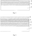
Figure 2 is a schematic view showingStep 1 of the manufacturing method of flexible array substrate provided by the first embodiment of the present invention; -
Figure 3 is a schematic view showingStep 2 of the manufacturing method of flexible array substrate provided by the first embodiment of the present invention; -
Figure 4 and Figure 5 are schematicviews showing Step 3 of the manufacturing method of flexible array substrate provided by the first embodiment of the present invention; -
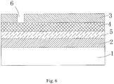
Figure 6 is a schematic view showingStep 4 of the manufacturing method of flexible array substrate provided by the first embodiment of the present invention; -
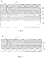
Figure 7 is a schematic view showingStep 5 of the manufacturing method of flexible array substrate provided by the first embodiment of the present invention; -
Figure 8 is a schematic view showingStep 6 of the manufacturing method of flexible array substrate provided by the first embodiment of the present invention; -
Figure 9 is a schematic view showing the flowchart of the manufacturing method of flexible array substrate provided by the first embodiment of the present invention. - To further explain the technique means and effect of the present invention, the following uses preferred embodiments and drawings for detailed description.
- Referring to
Figure 9 , the present invention provides a manufacturing method of flexible array substrate, which comprises: - Step 1: referring to
Figure 2 , providing arigid support plate 1 and aflexible substrate 3, adhering theflexible substrate 3 to therigid support plate 1 with anadhesive layer 2 so that the back side of theflexible substrate 3 facing away from therigid support plate 1.
Specifically, therigid support plate 1 is made of glass; the material of theflexible substrate 3 is polyimide (PI), polyethylene terephthalate (PET), cycloolefin copolymer (COC), or polyether resin (PES); the thickness of the flexible substrate is 10-300µm, which facilitates the subsequent drilling of holes. Theadhesive layer 2 can be made of pressure-sensitive glue or temperature-controlled glue. - Step 2: referring to
Figure 3 , forming a backside driver circuit 4 on the back side of theflexible substrate 3 and covering aprotective layer 5 on the backside driver circuit 4.
Specifically, theprotective layer 5 is made with an inorganic oxide deposition process or an organic material coating process. - Step 3: referring to
Figure 4 , separating theflexible substrate 3 from therigid support plate 1, turning theflexible substrate 3 over and adhering theflexible substrate 3 to therigid support plate 1 with theadhesive layer 2 so that the front side of theflexible substrate 3 facing away from therigid support plate 1, with theprotective layer 5 contacting theadhesive layer 2.
Specifically, inStep 3, theflexible substrate 3 is separated from therigid support plate 1 by a laser peeling process. Alternatively, theadhesive layer 2 is made of a temperature-controlled glue, and separating theflexible substrate 3 from therigid support plate 1 is by changing the temperature of theadhesive layer 2. - Step 4: referring to
Figure 6 , formingholes 6 penetrating theflexible substrate 3 in a predefined non-active area on the front side of theflexible substrate 3, exposing the backside driver circuit 4 on the back side of theflexible substrate 3.
Specifically, inStep 4, theholes 6 are formed by a laser drilling process or a chemistry etching process. The diameter of the holes must match the diameter of the wires to be passing through theholes 6; and preferably, the diameter of the hole is 5-100µm. - Step 5: referring to
Figure 7 , forming a frontside driver circuit 7 and a display circuit respectively on the predefined non-active area and active area on the front side of theflexible substrate 3, the frontside driver circuit 7 being electrically connected to the display circuit, and the backside driver circuit 4 being electrically connected to the display circuit through theholes 6.
Specifically, because the thickness of theflexible substrate 3 is much reduced than the thickness of the known glass substrate, the yield rate ofStep 4 of formingholes 6 andStep 5 of forming wires to connect the backside driver circuit 4 to the display circuit in theholes 6 can be ensured so that the process can proceed.
Specifically, the active area is located at the center of theflexible substrate 3, and the non-active area surrounding the active area. The frontside driver circuit 7 and the backside driver circuit 4 together form the wire on array (WOA) of the flexible array substrate. The display circuit comprises a plurality of data lines and a plurality of scan lines; the data lines and the scan lines intersect perpendicularly to form a plurality of pixel units. Each wire of the WOA corresponds to a data line or a scan line. Each wire receives a scan signal or data signal externally and transports to the corresponding scan line or data line to achieve displaying.
It should be noted that the present invention is also applicable to array substrate using GOA technology. At this point, the frontside driver circuit 7 and the backside driver circuit 4 together form the wire on array (WOA) and the gate driver on array (GOA) circuit of the flexible array substrate. The GOA circuit comprises a plurality of GOA units, with each corresponding to a scan line. Each wire of WOA is electrically connected to a data line or a GOA unit. Each wire passes the received external signal to the GOA unit to generate a scan signal, which is passed to the scan line, or receives a data line and passes to a data line to achieve displaying. The GOA technology eliminates the need for external gate driver chip to further reduce the border width of the display.
It should be noted that by distributing the circuit structure in the non-active area (comprising WOA and GOA) to both sides of the flexible substrate can greatly reduce the area in the non-active area occupied by the circuit structure compared to placing only on one side of the flexible substrate. As such, the width of the non-active area is reduced to achieve ultra-narrow border or borderless display. - Step 6: separating the
flexible substrate 3 from therigid support plate 1 to obtain the flexile array substrate. - Specifically, in
Step 6, theflexible substrate 3 is separated from therigid support plate 1 by a laser peeling process. Alternatively, theadhesive layer 2 is made of a temperature-controlled glue, and separating theflexible substrate 3 from therigid support plate 1 is by changing the temperature of theadhesive layer 2. - In summary, the present invention provides a manufacturing method of flexible array substrate. The method comprises: adhering the flexible substrate to the rigid support plate to manufacture the back side driver circuit and the protective layer on the back side driver circuit; peeling the flexible substrate off, turning the flexible substrate over and then adhering again to the rigid supporting plate to manufacture the protecting layer and the adhesive layer; forming holes, front side driver circuit and display circuit on the flexible substrate, the back side driver circuit electrically connected to the display circuit and the back side driver circuit electrically connected to the display circuit through the holes to obtain a flexible array substrate with double-sided circuit structure. By distributing the circuit structure of the non-active area to both sides of the flexible substrate, the width of the non-active area can be reduced to realize an ultra-narrow border or borderless display.
- It should be noted that in the present disclosure the terms, such as, first, second are only for distinguishing an entity or operation from another entity or operation, and does not imply any specific relation or order between the entities or operations. Also, the terms "comprises", "include", and other similar variations, do not exclude the inclusion of other non-listed elements. Without further restrictions, the expression "comprises a..." does not exclude other identical elements from presence besides the listed elements.
- Embodiments of the present invention have been described, but not intending to impose any unduly constraint to the appended claims. Any modification of equivalent structure or equivalent process made according to the disclosure and drawings of the present invention, or any application thereof, directly or indirectly, to other related fields of technique, is considered encompassed in the scope of protection defined by the clams of the present invention.
wherein the material of the flexible substrate being polyimide, polyethylene terephthalate, cycloolefin copolymer, or polyether resin;
wherein the thickness of the flexible substrate is 10-300µm.
Claims (17)
- A manufacturing method of flexible array substrate, which comprises:Step 1: providing a rigid support plate and a flexible substrate, adhering the flexible substrate to the rigid support plate with an adhesive layer so that the back side of the flexible substrate facing away from the rigid support plate;Step 2: forming a back side driver circuit on the back side of the flexible substrate and covering a protective layer on the back side driver circuit;Step 3: separating the flexible substrate from the rigid support plate, turning the flexible substrate over and adhering the flexible substrate to the rigid support plate with the adhesive layer so that the front side of the flexible substrate facing away from the rigid support plate, with the protective layer contacting the adhesive layer;Step 4: forming holes penetrating the flexible substrate in a predefined non-active area on the front side of the flexible substrate, exposing the back side driver circuit on the back side of the flexible substrate;Step 5: forming a front side driver circuit and a display circuit respectively on the predefined non-active area and active area on the front side of the flexible substrate, the front side driver circuit being electrically connected to the display circuit, and the back side driver circuit being electrically connected to the display circuit through the holes;Step 6: separating the flexible substrate from the rigid support plate to obtain the flexile array substrate.
- The manufacturing method of flexible array substrate as claimed in Claim 1,
wherein the rigid support plat is made of glass. - The manufacturing method of flexible array substrate as claimed in Claim 1,
wherein the material of the flexible substrate is polyimide, polyethylene terephthalate, cycloolefin copolymer, or polyether resin. - The manufacturing method of flexible array substrate as claimed in Claim 1,
wherein the thickness of the flexible substrate is 10-300µm. - The manufacturing method of flexible array substrate as claimed in Claim 1,
wherein in Step 4, the holes are formed by a laser drilling process or a chemistry etching process. - The manufacturing method of flexible array substrate as claimed in Claim 1, wherein the diameter of the hole is 5-100µm.
- The manufacturing method of flexible array substrate as claimed in Claim 1, wherein in Step 3 and Step 6, the flexible substrate is separated from the rigid support plate by a laser peeling process.
- The manufacturing method of flexible array substrate as claimed in Claim 1, wherein the adhesive layer is made of a temperature-controlled glue, and in Step 3 and Step 6, separating the flexible substrate from the rigid support plate is by changing the temperature of the adhesive layer.
- The manufacturing method of flexible array substrate as claimed in Claim 1, wherein the front side driver circuit and the back side driver circuit together form the wire on array (WOA) of the flexible array substrate.
- The manufacturing method of flexible array substrate as claimed in Claim 1, wherein the front side driver circuit and the back side driver circuit together form the wire on array (WOA) and the gate driver on array (GOA) circuit of the flexible array substrate.
- A manufacturing method of flexible array substrate, which comprises:Step 1: providing a rigid support plate and a flexible substrate, adhering the flexible substrate to the rigid support plate with an adhesive layer so that the back side of the flexible substrate facing away from the rigid support plate;Step 2: forming a back side driver circuit on the back side of the flexible substrate and covering a protective layer on the back side driver circuit;Step 3: separating the flexible substrate from the rigid support plate, turning the flexible substrate over and adhering the flexible substrate to the rigid support plate with the adhesive layer so that the front side of the flexible substrate facing away from the rigid support plate, with the protective layer contacting the adhesive layer;Step 4: forming holes penetrating the flexible substrate in a predefined non-active area on the front side of the flexible substrate, exposing the back side driver circuit on the back side of the flexible substrate;Step 5: forming a front side driver circuit and a display circuit respectively on the predefined non-active area and active area on the front side of the flexible substrate, the front side driver circuit being electrically connected to the display circuit, and the back side driver circuit being electrically connected to the display circuit through the holes;Step 6: separating the flexible substrate from the rigid support plate to obtain the flexile array substrate;wherein the rigid support plat is made of glass;
wherein the material of the flexible substrate is polyimide, polyethylene terephthalate, cycloolefin copolymer, or polyether resin;
wherein the thickness of the flexible substrate is 10-300µm. - The manufacturing method of flexible array substrate as claimed in Claim 11, wherein in Step 4, the holes are formed by a laser drilling process or a chemistry etching process.
- The manufacturing method of flexible array substrate as claimed in Claim 11, wherein the diameter of the hole is 5-100µm.
- The manufacturing method of flexible array substrate as claimed in Claim 11, wherein in Step 3 and Step 6, the flexible substrate is separated from the rigid support plate by a laser peeling process.
- The manufacturing method of flexible array substrate as claimed in Claim 11, wherein the adhesive layer is made of a temperature-controlled glue, and in Step 3 and Step 6, separating the flexible substrate from the rigid support plate is by changing the temperature of the adhesive layer.
- The manufacturing method of flexible array substrate as claimed in Claim 11, wherein the front side driver circuit and the back side driver circuit together form the wire on array (WOA) of the flexible array substrate.
- The manufacturing method of flexible array substrate as claimed in Claim 11, wherein the front side driver circuit and the back side driver circuit together form the wire on array (WOA) and the gate driver on array (GOA) circuit of the flexible array substrate.
Applications Claiming Priority (2)
| Application Number | Priority Date | Filing Date | Title |
|---|---|---|---|
| CN201611184975.XA CN106530972B (en) | 2016-12-20 | 2016-12-20 | The preparation method of flexible array substrate |
| PCT/CN2016/113371 WO2018113025A1 (en) | 2016-12-20 | 2016-12-30 | Method for manufacturing flexible array substrate |
Publications (3)
| Publication Number | Publication Date |
|---|---|
| EP3561799A1 true EP3561799A1 (en) | 2019-10-30 |
| EP3561799A4 EP3561799A4 (en) | 2020-06-17 |
| EP3561799B1 EP3561799B1 (en) | 2021-07-28 |
Family
ID=58341264
Family Applications (1)
| Application Number | Title | Priority Date | Filing Date |
|---|---|---|---|
| EP16924891.1A Active EP3561799B1 (en) | 2016-12-20 | 2016-12-30 | Method for manufacturing flexible array substrate |
Country Status (6)
| Country | Link |
|---|---|
| US (1) | US10477689B2 (en) |
| EP (1) | EP3561799B1 (en) |
| JP (1) | JP6742523B2 (en) |
| KR (1) | KR102263432B1 (en) |
| CN (1) | CN106530972B (en) |
| WO (1) | WO2018113025A1 (en) |
Families Citing this family (10)
| Publication number | Priority date | Publication date | Assignee | Title |
|---|---|---|---|---|
| CN106773384A (en) * | 2016-12-20 | 2017-05-31 | 深圳市华星光电技术有限公司 | Goa circuit structure |
| CN106952583B (en) * | 2017-05-23 | 2019-04-30 | 深圳市华星光电技术有限公司 | The production method of flexible array substrate |
| CN107731102A (en) * | 2017-10-31 | 2018-02-23 | 云谷(固安)科技有限公司 | The method for assembling and camber display screen of a kind of camber display screen |
| CN108122497B (en) * | 2018-02-02 | 2023-11-14 | 京东方科技集团股份有限公司 | A flexible array substrate, flexible display device and assembly method |
| CN109192077B (en) * | 2018-11-07 | 2019-09-03 | 深圳秋田微电子股份有限公司 | The production method of flexible liquid crystal device |
| CN111383522B (en) * | 2018-12-29 | 2022-12-02 | 北京小米移动软件有限公司 | Display screen and electronic equipment |
| CN110473965A (en) * | 2019-08-27 | 2019-11-19 | 深圳市华星光电半导体显示技术有限公司 | The preparation method of flexible OLED display panel and flexible OLED display panel |
| CN110890050B (en) * | 2019-11-21 | 2022-07-12 | 武汉华星光电半导体显示技术有限公司 | Array substrate, manufacturing method thereof and display device |
| CN111445803B (en) * | 2020-05-14 | 2023-04-14 | 京东方科技集团股份有限公司 | display device |
| CN116052548A (en) * | 2022-12-15 | 2023-05-02 | 康佳集团股份有限公司 | Flexible Micro-LED display for wearable devices, manufacturing method, and wearable devices |
Family Cites Families (20)
| Publication number | Priority date | Publication date | Assignee | Title |
|---|---|---|---|---|
| US6036809A (en) * | 1999-02-16 | 2000-03-14 | International Business Machines Corporation | Process for releasing a thin-film structure from a substrate |
| JP4321700B2 (en) * | 2002-11-06 | 2009-08-26 | 大日本印刷株式会社 | Method for producing functional element |
| JP3961537B2 (en) * | 2004-07-07 | 2007-08-22 | 日本電気株式会社 | Manufacturing method of semiconductor mounting wiring board and manufacturing method of semiconductor package |
| KR20080043507A (en) * | 2006-11-14 | 2008-05-19 | 엘지디스플레이 주식회사 | Flexible display device and method of manufacturing the same |
| JP2008159934A (en) * | 2006-12-25 | 2008-07-10 | Kyodo Printing Co Ltd | Flexible TFT substrate, manufacturing method thereof and flexible display |
| KR20090017014A (en) * | 2007-08-13 | 2009-02-18 | 삼성전자주식회사 | Manufacturing Method of Flexible Display |
| KR101490485B1 (en) * | 2008-10-30 | 2015-02-05 | 삼성디스플레이 주식회사 | Liquid crystal display and method of manufacturing the same |
| JP5338410B2 (en) * | 2009-03-19 | 2013-11-13 | 日立化成株式会社 | Wiring board manufacturing method |
| US20100289132A1 (en) * | 2009-05-13 | 2010-11-18 | Shih-Fu Huang | Substrate having embedded single patterned metal layer, and package applied with the same, and methods of manufacturing of the substrate and package |
| US8367473B2 (en) * | 2009-05-13 | 2013-02-05 | Advanced Semiconductor Engineering, Inc. | Substrate having single patterned metal layer exposing patterned dielectric layer, chip package structure including the substrate, and manufacturing methods thereof |
| CN102013414A (en) * | 2009-09-08 | 2011-04-13 | 群康科技(深圳)有限公司 | Making method of flexible display assembly |
| US8786062B2 (en) * | 2009-10-14 | 2014-07-22 | Advanced Semiconductor Engineering, Inc. | Semiconductor package and process for fabricating same |
| JP5757083B2 (en) * | 2010-12-01 | 2015-07-29 | セイコーエプソン株式会社 | Thin film transistor forming substrate, semiconductor device, electric device |
| CN201928507U (en) * | 2010-12-07 | 2011-08-10 | 何忠亮 | Double-sided circuit board |
| JP2013040981A (en) * | 2011-08-11 | 2013-02-28 | Sony Corp | Display device and electronic apparatus |
| CN102625581B (en) * | 2012-03-14 | 2014-11-05 | 华为终端有限公司 | Flexible circuit board and manufacturing method thereof |
| CN203012296U (en) * | 2012-12-13 | 2013-06-19 | 京东方科技集团股份有限公司 | Array substrate and liquid crystal display device |
| KR102291865B1 (en) * | 2015-01-16 | 2021-08-20 | 삼성디스플레이 주식회사 | Flexible display device and method of manufacturing the same |
| CN104916252B (en) * | 2015-07-13 | 2017-08-25 | 京东方科技集团股份有限公司 | Circular display panel and preparation method thereof, display device |
| CN105632347A (en) * | 2016-04-01 | 2016-06-01 | 京东方科技集团股份有限公司 | Flexible panel and manufacture method thereof and display device |
-
2016
- 2016-12-20 CN CN201611184975.XA patent/CN106530972B/en active Active
- 2016-12-30 KR KR1020197021197A patent/KR102263432B1/en active Active
- 2016-12-30 US US15/503,704 patent/US10477689B2/en not_active Expired - Fee Related
- 2016-12-30 EP EP16924891.1A patent/EP3561799B1/en active Active
- 2016-12-30 JP JP2019533224A patent/JP6742523B2/en active Active
- 2016-12-30 WO PCT/CN2016/113371 patent/WO2018113025A1/en not_active Ceased
Also Published As
| Publication number | Publication date |
|---|---|
| WO2018113025A1 (en) | 2018-06-28 |
| US10477689B2 (en) | 2019-11-12 |
| JP6742523B2 (en) | 2020-08-19 |
| CN106530972B (en) | 2017-12-29 |
| JP2020504444A (en) | 2020-02-06 |
| US20180213648A1 (en) | 2018-07-26 |
| KR102263432B1 (en) | 2021-06-14 |
| EP3561799A4 (en) | 2020-06-17 |
| KR20190097223A (en) | 2019-08-20 |
| CN106530972A (en) | 2017-03-22 |
| EP3561799B1 (en) | 2021-07-28 |
Similar Documents
| Publication | Publication Date | Title |
|---|---|---|
| EP3561799B1 (en) | Method for manufacturing flexible array substrate | |
| US11304294B2 (en) | Display device | |
| EP3561585B1 (en) | Display device | |
| US10429681B1 (en) | Structure of GOA circuit | |
| JP6845351B2 (en) | Manufacturing method of flexible array substrate | |
| KR20080054175A (en) | Manufacturing method of liquid crystal display device | |
| KR102283144B1 (en) | Display device | |
| KR20200017441A (en) | Display device |
Legal Events
| Date | Code | Title | Description |
|---|---|---|---|
| STAA | Information on the status of an ep patent application or granted ep patent |
Free format text: STATUS: THE INTERNATIONAL PUBLICATION HAS BEEN MADE |
|
| PUAI | Public reference made under article 153(3) epc to a published international application that has entered the european phase |
Free format text: ORIGINAL CODE: 0009012 |
|
| STAA | Information on the status of an ep patent application or granted ep patent |
Free format text: STATUS: REQUEST FOR EXAMINATION WAS MADE |
|
| 17P | Request for examination filed |
Effective date: 20190705 |
|
| AK | Designated contracting states |
Kind code of ref document: A1 Designated state(s): AL AT BE BG CH CY CZ DE DK EE ES FI FR GB GR HR HU IE IS IT LI LT LU LV MC MK MT NL NO PL PT RO RS SE SI SK SM TR |
|
| AX | Request for extension of the european patent |
Extension state: BA ME |
|
| DAV | Request for validation of the european patent (deleted) | ||
| DAX | Request for extension of the european patent (deleted) | ||
| REG | Reference to a national code |
Ref country code: DE Ref legal event code: R079 Ref document number: 602016061444 Country of ref document: DE Free format text: PREVIOUS MAIN CLASS: G09F0009300000 Ipc: G02F0001133300 |
|
| A4 | Supplementary search report drawn up and despatched |
Effective date: 20200520 |
|
| RIC1 | Information provided on ipc code assigned before grant |
Ipc: G02F 1/1333 20060101AFI20200514BHEP Ipc: G09F 9/30 20060101ALI20200514BHEP Ipc: H01L 51/00 20060101ALI20200514BHEP Ipc: G02F 1/1345 20060101ALI20200514BHEP |
|
| GRAP | Despatch of communication of intention to grant a patent |
Free format text: ORIGINAL CODE: EPIDOSNIGR1 |
|
| STAA | Information on the status of an ep patent application or granted ep patent |
Free format text: STATUS: GRANT OF PATENT IS INTENDED |
|
| INTG | Intention to grant announced |
Effective date: 20210309 |
|
| GRAS | Grant fee paid |
Free format text: ORIGINAL CODE: EPIDOSNIGR3 |
|
| GRAA | (expected) grant |
Free format text: ORIGINAL CODE: 0009210 |
|
| STAA | Information on the status of an ep patent application or granted ep patent |
Free format text: STATUS: THE PATENT HAS BEEN GRANTED |
|
| AK | Designated contracting states |
Kind code of ref document: B1 Designated state(s): AL AT BE BG CH CY CZ DE DK EE ES FI FR GB GR HR HU IE IS IT LI LT LU LV MC MK MT NL NO PL PT RO RS SE SI SK SM TR |
|
| REG | Reference to a national code |
Ref country code: GB Ref legal event code: FG4D |
|
| REG | Reference to a national code |
Ref country code: CH Ref legal event code: EP |
|
| REG | Reference to a national code |
Ref country code: DE Ref legal event code: R096 Ref document number: 602016061444 Country of ref document: DE |
|
| REG | Reference to a national code |
Ref country code: AT Ref legal event code: REF Ref document number: 1415227 Country of ref document: AT Kind code of ref document: T Effective date: 20210815 |
|
| REG | Reference to a national code |
Ref country code: IE Ref legal event code: FG4D |
|
| REG | Reference to a national code |
Ref country code: LT Ref legal event code: MG9D |
|
| REG | Reference to a national code |
Ref country code: NL Ref legal event code: MP Effective date: 20210728 |
|
| REG | Reference to a national code |
Ref country code: AT Ref legal event code: MK05 Ref document number: 1415227 Country of ref document: AT Kind code of ref document: T Effective date: 20210728 |
|
| PG25 | Lapsed in a contracting state [announced via postgrant information from national office to epo] |
Ref country code: PT Free format text: LAPSE BECAUSE OF FAILURE TO SUBMIT A TRANSLATION OF THE DESCRIPTION OR TO PAY THE FEE WITHIN THE PRESCRIBED TIME-LIMIT Effective date: 20211129 Ref country code: NL Free format text: LAPSE BECAUSE OF FAILURE TO SUBMIT A TRANSLATION OF THE DESCRIPTION OR TO PAY THE FEE WITHIN THE PRESCRIBED TIME-LIMIT Effective date: 20210728 Ref country code: NO Free format text: LAPSE BECAUSE OF FAILURE TO SUBMIT A TRANSLATION OF THE DESCRIPTION OR TO PAY THE FEE WITHIN THE PRESCRIBED TIME-LIMIT Effective date: 20211028 Ref country code: HR Free format text: LAPSE BECAUSE OF FAILURE TO SUBMIT A TRANSLATION OF THE DESCRIPTION OR TO PAY THE FEE WITHIN THE PRESCRIBED TIME-LIMIT Effective date: 20210728 Ref country code: FI Free format text: LAPSE BECAUSE OF FAILURE TO SUBMIT A TRANSLATION OF THE DESCRIPTION OR TO PAY THE FEE WITHIN THE PRESCRIBED TIME-LIMIT Effective date: 20210728 Ref country code: ES Free format text: LAPSE BECAUSE OF FAILURE TO SUBMIT A TRANSLATION OF THE DESCRIPTION OR TO PAY THE FEE WITHIN THE PRESCRIBED TIME-LIMIT Effective date: 20210728 Ref country code: LT Free format text: LAPSE BECAUSE OF FAILURE TO SUBMIT A TRANSLATION OF THE DESCRIPTION OR TO PAY THE FEE WITHIN THE PRESCRIBED TIME-LIMIT Effective date: 20210728 Ref country code: AT Free format text: LAPSE BECAUSE OF FAILURE TO SUBMIT A TRANSLATION OF THE DESCRIPTION OR TO PAY THE FEE WITHIN THE PRESCRIBED TIME-LIMIT Effective date: 20210728 Ref country code: BG Free format text: LAPSE BECAUSE OF FAILURE TO SUBMIT A TRANSLATION OF THE DESCRIPTION OR TO PAY THE FEE WITHIN THE PRESCRIBED TIME-LIMIT Effective date: 20211028 Ref country code: RS Free format text: LAPSE BECAUSE OF FAILURE TO SUBMIT A TRANSLATION OF THE DESCRIPTION OR TO PAY THE FEE WITHIN THE PRESCRIBED TIME-LIMIT Effective date: 20210728 Ref country code: SE Free format text: LAPSE BECAUSE OF FAILURE TO SUBMIT A TRANSLATION OF THE DESCRIPTION OR TO PAY THE FEE WITHIN THE PRESCRIBED TIME-LIMIT Effective date: 20210728 |
|
| PG25 | Lapsed in a contracting state [announced via postgrant information from national office to epo] |
Ref country code: PL Free format text: LAPSE BECAUSE OF FAILURE TO SUBMIT A TRANSLATION OF THE DESCRIPTION OR TO PAY THE FEE WITHIN THE PRESCRIBED TIME-LIMIT Effective date: 20210728 Ref country code: LV Free format text: LAPSE BECAUSE OF FAILURE TO SUBMIT A TRANSLATION OF THE DESCRIPTION OR TO PAY THE FEE WITHIN THE PRESCRIBED TIME-LIMIT Effective date: 20210728 Ref country code: GR Free format text: LAPSE BECAUSE OF FAILURE TO SUBMIT A TRANSLATION OF THE DESCRIPTION OR TO PAY THE FEE WITHIN THE PRESCRIBED TIME-LIMIT Effective date: 20211029 |
|
| PG25 | Lapsed in a contracting state [announced via postgrant information from national office to epo] |
Ref country code: DK Free format text: LAPSE BECAUSE OF FAILURE TO SUBMIT A TRANSLATION OF THE DESCRIPTION OR TO PAY THE FEE WITHIN THE PRESCRIBED TIME-LIMIT Effective date: 20210728 |
|
| REG | Reference to a national code |
Ref country code: DE Ref legal event code: R097 Ref document number: 602016061444 Country of ref document: DE |
|
| PG25 | Lapsed in a contracting state [announced via postgrant information from national office to epo] |
Ref country code: SM Free format text: LAPSE BECAUSE OF FAILURE TO SUBMIT A TRANSLATION OF THE DESCRIPTION OR TO PAY THE FEE WITHIN THE PRESCRIBED TIME-LIMIT Effective date: 20210728 Ref country code: SK Free format text: LAPSE BECAUSE OF FAILURE TO SUBMIT A TRANSLATION OF THE DESCRIPTION OR TO PAY THE FEE WITHIN THE PRESCRIBED TIME-LIMIT Effective date: 20210728 Ref country code: RO Free format text: LAPSE BECAUSE OF FAILURE TO SUBMIT A TRANSLATION OF THE DESCRIPTION OR TO PAY THE FEE WITHIN THE PRESCRIBED TIME-LIMIT Effective date: 20210728 Ref country code: EE Free format text: LAPSE BECAUSE OF FAILURE TO SUBMIT A TRANSLATION OF THE DESCRIPTION OR TO PAY THE FEE WITHIN THE PRESCRIBED TIME-LIMIT Effective date: 20210728 Ref country code: CZ Free format text: LAPSE BECAUSE OF FAILURE TO SUBMIT A TRANSLATION OF THE DESCRIPTION OR TO PAY THE FEE WITHIN THE PRESCRIBED TIME-LIMIT Effective date: 20210728 Ref country code: AL Free format text: LAPSE BECAUSE OF FAILURE TO SUBMIT A TRANSLATION OF THE DESCRIPTION OR TO PAY THE FEE WITHIN THE PRESCRIBED TIME-LIMIT Effective date: 20210728 |
|
| PLBE | No opposition filed within time limit |
Free format text: ORIGINAL CODE: 0009261 |
|
| STAA | Information on the status of an ep patent application or granted ep patent |
Free format text: STATUS: NO OPPOSITION FILED WITHIN TIME LIMIT |
|
| REG | Reference to a national code |
Ref country code: DE Ref legal event code: R119 Ref document number: 602016061444 Country of ref document: DE |
|
| 26N | No opposition filed |
Effective date: 20220429 |
|
| PG25 | Lapsed in a contracting state [announced via postgrant information from national office to epo] |
Ref country code: MC Free format text: LAPSE BECAUSE OF FAILURE TO SUBMIT A TRANSLATION OF THE DESCRIPTION OR TO PAY THE FEE WITHIN THE PRESCRIBED TIME-LIMIT Effective date: 20210728 Ref country code: IT Free format text: LAPSE BECAUSE OF FAILURE TO SUBMIT A TRANSLATION OF THE DESCRIPTION OR TO PAY THE FEE WITHIN THE PRESCRIBED TIME-LIMIT Effective date: 20210728 |
|
| REG | Reference to a national code |
Ref country code: CH Ref legal event code: PL |
|
| GBPC | Gb: european patent ceased through non-payment of renewal fee |
Effective date: 20211230 |
|
| REG | Reference to a national code |
Ref country code: BE Ref legal event code: MM Effective date: 20211231 |
|
| PG25 | Lapsed in a contracting state [announced via postgrant information from national office to epo] |
Ref country code: LU Free format text: LAPSE BECAUSE OF NON-PAYMENT OF DUE FEES Effective date: 20211230 Ref country code: IE Free format text: LAPSE BECAUSE OF NON-PAYMENT OF DUE FEES Effective date: 20211230 Ref country code: GB Free format text: LAPSE BECAUSE OF NON-PAYMENT OF DUE FEES Effective date: 20211230 Ref country code: DE Free format text: LAPSE BECAUSE OF NON-PAYMENT OF DUE FEES Effective date: 20220701 |
|
| PG25 | Lapsed in a contracting state [announced via postgrant information from national office to epo] |
Ref country code: FR Free format text: LAPSE BECAUSE OF NON-PAYMENT OF DUE FEES Effective date: 20211231 Ref country code: BE Free format text: LAPSE BECAUSE OF NON-PAYMENT OF DUE FEES Effective date: 20211231 |
|
| PG25 | Lapsed in a contracting state [announced via postgrant information from national office to epo] |
Ref country code: LI Free format text: LAPSE BECAUSE OF NON-PAYMENT OF DUE FEES Effective date: 20211231 Ref country code: CH Free format text: LAPSE BECAUSE OF NON-PAYMENT OF DUE FEES Effective date: 20211231 |
|
| PG25 | Lapsed in a contracting state [announced via postgrant information from national office to epo] |
Ref country code: CY Free format text: LAPSE BECAUSE OF FAILURE TO SUBMIT A TRANSLATION OF THE DESCRIPTION OR TO PAY THE FEE WITHIN THE PRESCRIBED TIME-LIMIT Effective date: 20210728 |
|
| PG25 | Lapsed in a contracting state [announced via postgrant information from national office to epo] |
Ref country code: HU Free format text: LAPSE BECAUSE OF FAILURE TO SUBMIT A TRANSLATION OF THE DESCRIPTION OR TO PAY THE FEE WITHIN THE PRESCRIBED TIME-LIMIT; INVALID AB INITIO Effective date: 20161230 |
|
| PG25 | Lapsed in a contracting state [announced via postgrant information from national office to epo] |
Ref country code: MK Free format text: LAPSE BECAUSE OF FAILURE TO SUBMIT A TRANSLATION OF THE DESCRIPTION OR TO PAY THE FEE WITHIN THE PRESCRIBED TIME-LIMIT Effective date: 20210728 |
|
| PG25 | Lapsed in a contracting state [announced via postgrant information from national office to epo] |
Ref country code: TR Free format text: LAPSE BECAUSE OF FAILURE TO SUBMIT A TRANSLATION OF THE DESCRIPTION OR TO PAY THE FEE WITHIN THE PRESCRIBED TIME-LIMIT Effective date: 20210728 |
|
| PG25 | Lapsed in a contracting state [announced via postgrant information from national office to epo] |
Ref country code: MT Free format text: LAPSE BECAUSE OF FAILURE TO SUBMIT A TRANSLATION OF THE DESCRIPTION OR TO PAY THE FEE WITHIN THE PRESCRIBED TIME-LIMIT Effective date: 20210728 |