EP3559988B1 - Substrat support pour composants électriques et procédé de fabrication d'un substrat support - Google Patents
Substrat support pour composants électriques et procédé de fabrication d'un substrat support Download PDFInfo
- Publication number
- EP3559988B1 EP3559988B1 EP17825198.9A EP17825198A EP3559988B1 EP 3559988 B1 EP3559988 B1 EP 3559988B1 EP 17825198 A EP17825198 A EP 17825198A EP 3559988 B1 EP3559988 B1 EP 3559988B1
- Authority
- EP
- European Patent Office
- Prior art keywords
- layer
- metal layer
- carrier substrate
- recesses
- primary
- Prior art date
- Legal status (The legal status is an assumption and is not a legal conclusion. Google has not performed a legal analysis and makes no representation as to the accuracy of the status listed.)
- Active
Links
Images








Classifications
-
- H—ELECTRICITY
- H10—SEMICONDUCTOR DEVICES; ELECTRIC SOLID-STATE DEVICES NOT OTHERWISE PROVIDED FOR
- H10W—GENERIC PACKAGES, INTERCONNECTIONS, CONNECTORS OR OTHER CONSTRUCTIONAL DETAILS OF DEVICES COVERED BY CLASS H10
- H10W40/00—Arrangements for thermal protection or thermal control
- H10W40/20—Arrangements for cooling
- H10W40/25—Arrangements for cooling characterised by their materials
- H10W40/255—Arrangements for cooling characterised by their materials having a laminate or multilayered structure, e.g. direct bond copper [DBC] ceramic substrates
Definitions
- the present invention relates to a carrier substrate for electrical, in particular electronic, components and a method for producing a carrier substrate.
- Carrier substrates are known, for example, as printed circuit boards or circuit boards. Electrical or electronic components and conductor tracks are typically arranged on one component side of the carrier substrate, whereby the electrical or electronic components and the conductor tracks can be connected together to form electrical circuits.
- carrier substrates that have an insulating layer with high electrical insulation strength for the electrical insulation of the individual electrical components and conductor tracks, such as a primary layer made of ceramic, have proven to be particularly advantageous.
- the electrical components When these carrier substrates are in operation, particularly when used in power electronics, the electrical components are typically subjected to such stress that they heat up and local heat sources form on the component side.
- the state of the art therefore includes heat sinks or cooling structures that are usually attached, e.g. soldered, to a cooling side opposite the component side, which is designed, for example, as a copper layer or copper base adjacent to the primary layer.
- the thermomechanical behavior of the carrier substrate during operation can disadvantageously lead to mechanical stresses in the carrier substrate.
- the JP-H 09260546 discloses a carrier substrate for electrical components, wherein a metal layer is provided, on the side of which facing the base body of the carrier substrate several evenly distributed recesses are formed.
- a carrier substrate is known whose metallization has a stepped course on the peripheral edge such that a recess is formed between the base body and the metallization on the peripheral outermost edge of the metallization.
- the WO 2013 186 267 A1 describes a mounting carrier for semiconductor chips, which has a second main surface provided for the mounting of semiconductor chips and a first main surface opposite the second main surface.
- the mounting carrier also has a mounting body, wherein the mounting body has a first metallization on the side facing the first main surface and the first main surface has a structure with a plurality of columnar structural elements.
- a carrier substrate for electrical components, in particular electronic components wherein the carrier substrate has a primary layer made of ceramic and at least one metal layer bonded to the primary layer, wherein the at least one metal layer has at least one, preferably several, recesses on the side facing the primary layer.
- the metal layer according to the invention has the advantage that the recesses influencing the thermal or thermomechanical behavior are arranged on the side facing the primary layer, in particular directly adjacent to the primary layer.
- the surface provided on the component side for connecting electrical or electronic components is not impaired or restricted, but is fully available to the user for attaching electronic components, wire bonds and/or terminals for supplying and discharging various electrical currents and voltages.
- the recesses have a positive effect on the carrier substrate by increasing the carrier substrate's resistance to thermal shock by up to 10 times, depending on their location, or by distributing mechanical stresses, so that, for example, local mechanical stress peaks in the edge area of the carrier substrate, in particular those originating from the primary layer, can be counteracted.
- These recesses can also be designed to be comparatively small in terms of their volume. This allows the arrangement of the recesses directly in the area in which the primary layer adjoins the metal layer and in which the greatest thermomechanically induced stresses arise.
- the manufacturing process can dispense with the introduction of the recess into the metal layer from the component side to the primary layer.
- the carrier substrate only has the primary layer and at least one metal layer, ie the carrier substrate is designed in two layers.
- the recesses facing the primary layer offer greater degrees of freedom in terms of their design, i.e. shape and arrangement, and the number of recesses introduced, since they are independent of the component side or surface, in particular independent of specifications by the component side.
- several rows of recesses can run from the edge of the metal layer into its central area.
- the recesses can extend over the entire thickness of the metal layer, i.e. be continuous, or only partially etched there, so that the metal layer is only locally weakened at certain points, preferably at the edge.
- the metal layer is a structured metal surface, such as a conductor track, on which electrical or electronic components can be mounted to form a circuit.
- the recesses are etched into the metal layer.
- the recesses are etched into the metal layer in particular before the metal layer is joined to the primary layer and then the metal layer is aligned during joining in such a way that the recesses lie on the primary side or border on the primary layer.
- the recesses are filled with a filling material, wherein the filling material in its intended state has in particular a lower coefficient of expansion and/or a higher modulus of elasticity than a material from which the metal layer is made.
- the filling material has a coefficient of linear expansion smaller than copper, i.e. ⁇ ⁇ 16.5 x 10 -6 K -1 , measured at room temperature.
- the filling material can advantageously be used to support or enable a subsequent joining process in which the carrier substrate is brought into its intended state by means of a material-to-material connection between the filling material and the metal layer on the one hand and between the filling material and the primary layer on the other.
- the filler material is selected in such a way that a lower combined coefficient of expansion (CTE) is established locally in the area of the edge profile, which partially shifts the thermomechanical stresses caused by the joining temperature during cooling after the joining process from the interface between the primary layer and the metal layer into the metal layer, in which the thermomechanical stresses can in turn be better reduced during cooling.
- CTE combined coefficient of expansion
- Possible filler materials include, for example, particle-filled soft solder, hard solder or active solder which contain 10 - 64 vol.%, preferably 20 - 50 vol.% and particularly preferably 30 - 50 vol.% of ceramic or metal particles with the properties described above, such as SiC, AIN, Al 2 O 3 , HPSX, BeO, Si 3 N 4 , ZnO, TiN, B 4 C, Mo, W, Cr, Ta or Nb.
- the primary layer has in particular an insulation layer with high electrical insulation strength, preferably of more than 5 kV/mm, particularly preferably of more than 10, 20 or even more than 30 kV/mm and/or with high thermal conductivity, preferably more than 10 W/mK, particularly preferably more than 20 or even more than 60 W/mK, such as technical ceramics or organic insulation materials filled with thermally conductive materials.
- an insulation layer with high electrical insulation strength preferably of more than 5 kV/mm, particularly preferably of more than 10, 20 or even more than 30 kV/mm and/or with high thermal conductivity, preferably more than 10 W/mK, particularly preferably more than 20 or even more than 60 W/mK, such as technical ceramics or organic insulation materials filled with thermally conductive materials.
- the side of the metal layer facing the component side, in particular the structured metal surface has a smooth, i.e. recess-free, surface at least in some areas.
- the recesses are designed such that a closed surface side of the structured metal surface facing the component side is larger than the contact surfaces via which the structured metal surface is in contact with or connected to the primary layer. It is also conceivable that the recesses are designed as hole-like and/or blind-hole-like, i.e. the recesses penetrate through the metal layer or open or end, preferably in the shape of a dome or cupola, in the interior of the metal layer.
- hole-like recesses and blind-hole-like bores are realized in the metal layer, wherein the number of hole-like recesses is smaller than the number of blind-hole-like recesses. Furthermore, it is preferably provided that in a projection direction or orientation running perpendicular to the main extension plane of the carrier substrate, no recesses or fewer recesses are arranged below a location or connection location provided for the component compared to the rest of the metal layer.
- the recess is arranged on the edge profile of the metal layer.
- the edge profile of the metal layer is preferably defined by a line along which the metal layer ends its direct contact with the primary layer.
- the edge profile, ie the edge line, or its surface is enlarged by the recesses, whereby mechanical stresses occurring during operation, in particular those originating from the primary layer, can be better distributed.
- the edge profile is in particular an outer circumference the edge layer in a plane running parallel to the main extension plane of the carrier substrate.
- the recess is let into an edge of the metal layer adjacent to the primary layer.
- the recess in the edge profile causes a contour that is set back by a maximum of one indentation depth.
- the average indentation depth ie the indentation depth averaged over the recesses in the edge profile, takes on a value between 50 ⁇ m and 1000 ⁇ m, preferably between 100 ⁇ m and 800 ⁇ m and particularly preferably between 150 ⁇ m and 600 ⁇ m.
- a ratio of a depth of the recess measured in the projection direction to the indentation depth assumes a value between 0.2 and 1.2, preferably between 0.3 and 1.0 and particularly preferably between 0.4 and 0.8.
- the edge region is the region in which 60% - 100%, preferably 80% - 100% of all recesses are arranged.
- several recesses in particular several recesses arranged next to one another, form a meandering, postage stamp-shaped and/or sawtooth-shaped edge profile of the metal layer, wherein in particular the meandering, postage stamp-shaped and/or sawtooth-shaped edge profile extends over the entire edge profile of the metal layer. It is also conceivable that the meandering, postage stamp-shaped and/or sawtooth-shaped edge profile of the metal layer extends only over a partial area of the entire edge profile of the metal layer or that several partial areas adjoin one another at a distance from one another as seen in the circumferential direction.
- the edge profile can also have irregular recesses, i.e., for example, small and large recesses that are mixed or arranged alternately with one another, or that are wavy, rectangular, parallelogram-shaped or jagged.
- a closed strip of the metal layer is formed along the edge profile, with the strip having the meandering, postage stamp-shaped and/or sawtooth-shaped edge profile, particularly towards one side.
- additional needle, dome or pin structures are arranged within the recesses in the edge profile, which connect the primary layer to the metal layer in order to homogenize the mechanical stress distribution or to distribute it over a larger area.
- the recess prefferably be designed as a curvature, in particular as a dome-like or partially dome-like curvature.
- the curvature is directed towards the side of the attached metal layer facing away from the primary layer. This advantageously prevents the recesses from appearing on the side of the metal layer facing away from the primary layer.
- the side of the metal layer facing away from the primary layer can thus be used entirely for components.
- the recesses in the central region of the metal layer form cavities between the metal layer and the primary layer.
- the metal layer forms an overhang, for example in a direction running perpendicular to the main extension plane.
- the recess to be designed to be oval, diamond-shaped, diamond-shaped or groove-shaped in a cross-section, in particular in a plane running parallel to the main extension plane.
- the recess has an average depth in a direction perpendicular to the main extension plane, which in relation to the smallest opening width of the recess, for example a diameter for a circular recess or a width of a trench-shaped recess, preferably assumes a value between 0.2 and 1.2, preferably between 0.3 and 1.0 and particularly preferably from 0.4 to 0.8. It is particularly preferred that the recesses are as small as possible with regard to the thermal behavior of the carrier substrate. It is also conceivable that the recesses are distributed over the entire metal layer. In this case, it is conceivable that the depths are distributed statistically or arbitrarily over the entire metal layer.
- the metal layer in the central region has a first partial region and a second partial region, wherein the number of recesses and/or the depth or size in the first partial region differs from the number of recesses and/or their depth or size in the second partial region.
- the first partial region and the second partial region are designed depending on the carrier substrate or its field of application.
- the average number and/or average depth of the recesses changes continuously across the metal layer.
- the number and/or depth of the recess increases or decreases in the direction of the edge of the metal layer.
- the ratio between the depth of the recesses and the thickness of the structured metal surface is between 2.5% and 70%, preferably between 5% and 60% and particularly preferably between 10% and 55%.
- the ratio of the depth of the recesses to the thickness of the metal layer refers to metal layer thicknesses between 200 ⁇ m and 2000 ⁇ m, preferably between 250 ⁇ m and 1500 ⁇ m and particularly preferably between 300 ⁇ m and 1000 ⁇ m.
- All other recesses that run parallel to the continuous, dome-shaped depression can be designed to be continuous or as several discrete recesses lying next to one another.
- a second distance of all further recesses from the recess has values between 100 ⁇ m and 1000 ⁇ m, preferably 110 ⁇ m and 600 ⁇ m and particularly preferably 150 ⁇ m and 400 ⁇ m.
- the depth of the recesses and the depth of the further recess is smaller than the thickness of the metal layer and preferably have values between 2.5% and 70%, preferably between 5% and 60% and particularly preferably between 10% and 55% of the metal layer thickness.
- recesses on the second side are arranged in a direction perpendicular to the main plane of extension, essentially congruent with or offset from the recesses on the first side of the intermediate layer.
- a comparatively resistant metal layer is provided, since local weakening of the metal layer is avoided.
- a sufficiently large intermediate layer can be provided beneath components, via which the heat from the components acting as a heat source can be effectively transported to the cooling side during operation.
- the intermediate layer has grooves, in particular etched grooves, lying opposite one another in an area adjacent to the edge profile on the first and second sides.
- the recess is let into cooling structures or parts of cooling structures that protrude from the primary layer and/or secondary layer in a direction parallel to the main extension plane.
- the cooling structure comprises a base body and a web region with webs running perpendicular to the main extension plane.
- the recess preferably encloses or surrounds an edge of the first primary layer and/or the secondary layer, in particular the edge of the primary layer and/or the secondary layer that faces the cooling structure, i.e. the recess forms a closed trench or a closed bead that surrounds the edge in the main extension plane.
- the metal layer is folded prior to joining.
- recesses are specifically made, preferably exclusively, on one side in the metal layer and then, by folding, the intermediate layer is provided with recesses that face the primary layer and the secondary layer in the manufactured state. This advantageously makes it possible to dispense with the complex etching of recesses on both sides in the metal layer.
- the recesses are etched into the metal layer in such a way that the recesses in the folded state are arranged essentially congruent with one another or offset from one another in a direction running perpendicular to the main extension plane.
- two or more sub-substrates separately in a first step using the joining methods already mentioned, such as the primary layer with the structured metal surface and part of the metallic intermediate layer, as well as the secondary layer with part of the metallic intermediate layer and the cooling structure.
- These at least two sub-substrates or individual laminates are joined to the substrate according to the invention in at least one further, e.g. second, joining step, using common joining processes.
- common joining processes such as DCB process, brazing, soft soldering, diffusion welding or a sintering process.
- the metal layer is etched on both sides, preferably simultaneously or with temporal overlap.
- narrower structures or recesses can be realized between the metal surfaces of the layout or the structured metal surfaces.
- thicker metal layers can be structured because, unlike in the prior art, they can be etched on both sides and congruent with one another. Congruent is to be understood as meaning that the recesses are arranged in alignment with one another with regard to their center, while the recesses can have different widths. It is preferably provided that the width of the iso-trench assumes a value that corresponds to a multiple of the thickness of the metal layer, preferably 2-10 times, particularly preferably 2-5 times the thickness of the metal layer.
- the thermal shock resistance can be increased by 5 to 10 times.
- a carrier substrate 1 for electrical components 13 is shown schematically in a sectional view.
- This is preferably a ceramic-containing carrier substrate 1 that is advantageous for special applications.
- the carrier substrate 1 has a component side 4 on which a metal layer, for example made of copper or aluminum, is provided for electrical components 13 or modules in the form of structured metal surfaces 2.
- a metal layer for example made of copper or aluminum
- the carrier substrate 1 can be virtually broken down into a primary substrate, a secondary substrate and preferably into a virtual intermediate substrate or part of an intermediate layer located therebetween, the primary substrate also comprising part of the metal layer and the intermediate layer in addition to the primary layer and the secondary substrate comprising part of the cooling structure and the intermediate layer.
- a thermomechanical symmetry between the primary substrate and the secondary substrate is sought, ie the thermal expansion coefficient (CTE) of both substrates should preferably be the same or at least similar, for example within a tolerance of +/- 20% or preferably +/- 10%, particularly preferably +/- 5%.
- the edge profile 32 of the metal layer, in particular of the structured metal surface 2 is profiled or structured on the side facing the primary layer 10, in particular on an edge.
- the edge profile 32 is advantageously designed to distribute the mechanical stresses that occur.
- the structured edge profile 32 is formed by recesses 5, in particular etched recesses 5, on the side of the metal layer facing the primary layer 10.
- the recesses 5 do not extend to the component side of the structured metal surface 2.
- the recesses 5 have a depth T of between 10% and 70% of the layer thickness MD of the structured metal surface 2.
- the contact side of the metal layer facing the primary layer 10 is indented by an indentation depth ET to the outermost edge profile 35 of the metal layer.
- the average indentation depth ET here assumes a value between 20 ⁇ m and 600 ⁇ m, preferably between 50 ⁇ m and 500 ⁇ m and particularly preferably between 200 ⁇ m and 400 ⁇ m.
- the intermediate layer 15 arranged between the primary layer 10 and the secondary layer 20 and designed as a metal layer has a structured edge profile 32, which is realized in particular by several etched recesses 5 on the side facing the primary layer 10 and/or the secondary layer 20 or their edge profiles of the intermediate layer 15.
- the contact side of the metal layer facing the primary layer 10 and/or the secondary layer 20 is recessed by a further recess depth ET to the outermost Edge profile 35 of the metal layer is indented. It is conceivable that the indentation depth ET of the structured metal surface 2 and the further indentation depth ET of the intermediate layer 15 essentially correspond to one another or differ.
- the further indentation depth ET on the side of the intermediate layer 15 facing the secondary layer 20 and the indentation depth ET on the side of the intermediate layer 15 facing the primary layer 10 correspond to one another or differ.
- the recesses 5 in the structured metal surface 2 and the recesses 5 in the intermediate layer are designed to be congruent with one another in a projection direction or orientation P running perpendicular to the main extension plane of the carrier element 1, or are offset from one another.
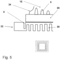
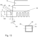
- a metallic cooling structure 30 connected to the secondary layer 20 on the cooling side 6 has an edge profile 32 structured by recesses 5.
- the indentation depth ET of the recesses 5 in the structured metal surface 2 and/or the further indentation depth ET of the recesses 5 in the intermediate layer 15 corresponds to an indentation depth ET in the cooling structure 30. It is also conceivable that the respective indentation depths are adapted to the individual application for which the carrier substrate 1 is intended.
- the structured metal surfaces 2, the metallic intermediate layer 15 and the cooling structure 30 are made of the metals Cu, Al, Mo, W, Ag, of alloys or composite materials of the metals mentioned, of special alloys such as Invar or Kovar or of composite materials of the metals mentioned filled with ceramic particles.
- the structured metal surfaces 2, the metallic intermediate layer 15 and the cooling structure 30 are made of copper or of aluminum or alloys and/or composite materials containing Cu and/or Al.
- the Primary layer 10 comprises Al 2 O 3 , ZrO 2 conversion-strengthened Al 2 O 3 , Si 3 N 4 , AIN, SiC, HPSX and/or BeO.
- the secondary layer 20 is preferably made of one of the aforementioned ceramics or molybdenum.
- Figure 2 is an edge profile 32 of the structured metal surface 2, the intermediate layer or cooling structure from the Figure 1 In particular, it is a meandering edge profile extending over the entire edge profile 32.
- a reduced top view of the carrier substrate 1 is shown in addition to the respective sectional views.
- a cutting line is shown as a dashed line, which can be assigned to the respective sectional view.
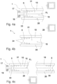
- FIGS 3a and 3b A second preferred and a third preferred embodiment of the intermediate layer 15 of an exemplary carrier substrate 1 according to the present invention are shown. It is conceivable that the intermediate layers 15 of the Figures 3a and 3b in a second and a third preferred embodiment of the carrier substrate 1, the intermediate layer 15 from Figure 1 can be replaced. In particular, in the case of the intermediate layers 15 from the Figures 3a and 3b provided that the metal layer designed as intermediate layer 15 has, in addition to the structured edge profile 32, recesses 5, in particular dome-shaped recesses 5, on the side facing the primary layer 10 and/or the secondary layer 20 in a central region 31.
- the recesses 5 are designed in such a way that, together with the primary layer 10 and/or the secondary layer 20, they form a cavity between the metal layer and the primary layer 10 and/or the secondary layer 20.
- the dome-shaped recesses 5 have a substantially circular cross-section, the diameter of which is between 100 ⁇ m and 1000 ⁇ m, preferably between 110 ⁇ m and 800 ⁇ m and particularly preferably between 150 ⁇ m and 600 ⁇ m. It is conceivable that the recesses 5 all have substantially the same diameter or that the sizes for the diameters are distributed statistically or randomly. Alternatively or additionally, it is conceivable that holes are let into the intermediate layer 15, which lead from the primary layer 10 to the secondary layer 20.
- both recesses 5 and hole-like recesses ie those that penetrate through the intermediate layer, are let into the intermediate layer 15, the ratio between hole-like recesses and blind hole-like recesses being less than 1, equal to 1 or greater than 1.
- recesses 5 are made on one side of a metal layer and then the metal layer is folded to form the intermediate layer 15.
- the folded metal layer forms a fold line FL and the recesses 5 are located on opposite sides of the intermediate layer 15.
- the recesses 5 on the first side 41 facing the primary layer 10 are arranged congruently with the recesses 5 on the second side 42 facing the secondary layer 20.
- the recesses 5 on the side facing the primary layer 10 are offset from the recesses 5 on the side facing the secondary layer 20 along a direction parallel to the main extension plane.
- the intermediate layers 15 from the Figures 3a and 3b It is provided that the edge profile 32 protrudes in a direction parallel to the main extension plane relative to the primary layer 10 and/or the secondary layer 20. As a result, the protruding section of the intermediate layer 15 can advantageously provide a contact element 16 with which a current can be introduced into the intermediate layer 15.
- FIGS 4a and 4b A fourth preferred and a fifth preferred embodiment of the intermediate layer 15 of an exemplary carrier substrate 1 according to the present invention are shown. It is conceivable that the Intermediate layers 15 of Figures 4a and 4b in a fourth and a fifth preferred embodiment of the carrier substrate 1, the intermediate layer 15 from Figure 1 is replaced in each case. In this case, the intermediate layer 15 is provided with a recess 5 within the intermediate layer 15.
- a hollow chamber 33 can be produced, for example, by etching two recesses 5 into a metal layer and then folding the metal layer to form the cavity within the intermediate layer 15 in such a way that the two recesses 5 are arranged congruently with one another on the folding side or along the folding line FL in the projection direction or orientation P.
- the two recesses 5 forming the cavity can, for example, be groove-shaped and/or dome-shaped.
- the intermediate layer 15 has a thickening 17 in the protruding section, which is provided for forming a contact element 16.
- the thickening 17 can be realized by an etching trench running parallel to the edge profile 32 of the intermediate layer 15, which is arranged on the side of the intermediate layer 15 facing the primary layer 10 and/or on the side of the intermediate layer 15 facing the secondary layer 20. It is also conceivable that two etching trenches are let into the metal layer and the thickening 17 is realized on the edge profile of the intermediate layer 15 by subsequently folding the metal layer. In the Figure 4b the edge profile 32 of the intermediate layer 15 is curved inwards.
- Such a stepped edge 34 can be realized, for example, by eroding the side surface of the intermediate layer 15, which faces neither the primary layer 10 nor the secondary layer 20, or in the case of a foldable intermediate layer 15 with a stepped edge profile, by etching.
- opposite edges of the intermediate layer 15 are provided with recesses of different widths, so that after folding in a direction perpendicular to the main extension plane, a stepped edge profile is formed on the side wall of the intermediate layer 15 It is also conceivable that further etching takes place in the area that forms the folding edge in the finished state or that immediately borders on it, in order to avoid mechanical stresses that would otherwise arise during later folding.
- the edge profile 32 of the intermediate layer 15 is designed such that the intermediate layer 15 has a section protruding from the primary layer 10 and/or the secondary layer 20 on one side and an inwardly curved edge region, i.e. a stepped edge 34, on the opposite side.
- a metal layer for a further preferred carrier substrate 1 is shown.
- the recess 5 is arranged on the side of the metal layer designed as a cooling structure 30 facing the secondary layer 20 and/or the primary layer 10.
- the recess 5 is arranged offset from the primary layer 10 and/or secondary layer 20 in a direction running parallel to the main extension plane, with the cooling structure 30 protruding from the primary layer 10 and/or the secondary layer 20.
- the recess is designed as an expansion joint in order to prevent the thermal expansion of the cooling structure 30 from causing mechanical stresses in the entire carrier substrate 1.
- FIG. 6 different arrangements of the recesses 5 in the metal layer are shown. Different cross-sectional shapes and arrangements in patterns are conceivable. In addition to circular cross-sections, a rectangular, a diamond-shaped, a wave-shaped and/or a triangular cross-section is also conceivable (first and second row). In addition, the Figure 6 Embodiments in which circular cross-sections with different diameters are arranged in different patterns (second and third row). Preferably, the circular cross-sections with different diameters arranged offset from each other.
- FIG. 7 A method for producing a recess 5 is shown schematically as an example. It is provided that the metal layer is etched on both sides, ie an etching process takes place both on the side of the metal layer adjacent to the primary layer 10 in the manufactured state and on the opposite side, in particular the intermediate layer 15. As the Figure 7 As can be seen, the recess 5 on the side facing the primary side 10 is etched first and then an iso-trench 7, which is intended in particular for forming a conductor track, is etched. It is also conceivable that these etching processes take place simultaneously or overlapping in time. By etching on both sides, it is also advantageously possible to accelerate the entire manufacturing process of the carrier substrate 1 and to create narrow iso-trenchs 7.
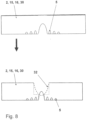
- FIG 8 Another method for producing a recess is shown schematically as an example. The method essentially corresponds to that of Figure 7 There is, however, a difference in the dimensions of the opposing etchings. It is preferably provided that the etching process on the side of the metal layer that is in contact with the primary layer 10 in the manufactured state is less intensive than the etching process on the opposite side. As a result, the recess 5 on the side associated with the primary layer 10 is smaller than that on the opposite side. By having the opposing etchings dimensioned differently, it is advantageously possible to implement a step etching with which the thermal shock resistance can be improved by a factor of between 5 and 10.
- a carrier substrate 1 according to an eighth exemplary embodiment of the present invention is shown in a detailed view.
- the Figure 8 The carrier substrate 1 shown comprises a closed etching trench 8, which extends parallel to the edge of the carrier substrate 1.
- the carrier substrate 1 also comprises an input channel 21 and an output channel 22 which are let into the metal layer and which connect the closed etching trenches 8 to an environment surrounding the carrier substrate 1.
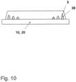
- Via the input channel 21 it is advantageously possible to introduce filler material into the closed etching trenches 8 after the primary layer 10 has been joined to the metal layer.
- the input channel 21 can advantageously be used to fill the closed etching trench 8 or further recesses 5 with functional materials, e.g. organic materials, inorganic binders or particle-filled materials. Filling after joining is particularly positive because the recesses 5 cannot be filled with a filler material before joining because they are not resistant to the temperature development that occurs during joining.
- the Figure 10 shows a further carrier substrate 1 according to the eighth preferred embodiment of the present invention. It shows the carrier substrate 1 from Figure 9 in a sectional view, wherein the recesses 5 are already filled with the filling material 38 before joining.
- the Figure 11 shows a sectional view through a metal layer 2, 15, 30 for a carrier substrate 1 according to a ninth embodiment of the present invention.
- a continuous trench-shaped depression is provided as the first recess 51, which runs parallel to the edge profile 35 of the metal layer 2, 15, 30 and ends in the metal layer 2, 15, 30 like a dome.
- the person skilled in the art understands the first recess 51 to mean in particular the first recess 5 let into the metal layer as seen from the edge profile 35 and spaced from the edge profile 35, or a first group of such recesses.
- one or more continuous first recesses 51 can be made next to one another in the metal layer 2, 15, 30 parallel to the edge profile 35 of the metal layer 2, 15, 30.
- the trench-shaped depression in the metal layer 2, 15, 30 has a first distance A from the edge profile 35 of the metal layer 2, 15, 30 from 100 ⁇ m to 1000 ⁇ m, preferably 110 ⁇ m to 600 ⁇ m and particularly preferably from 150 ⁇ m to 400 ⁇ m.
- All further recesses 52 which run parallel to the continuous fork-shaped depression can be designed to be continuous or as several discrete recesses lying next to one another.
- a second distance C of all further recesses 52 to the first recess 51 preferably has a value between 100 ⁇ m and 1000 ⁇ m, preferably between 110 ⁇ m and 600 ⁇ m and particularly preferably between 150 ⁇ m and 400 ⁇ m.
- the depth of the first recesses T 51 and the depth of the further recess T 52 is smaller than the thickness of the metal layer and preferably have values between 2.5% and 70%, preferably between 5% and 60% and particularly preferably between 10% and 55% of the metal layer thickness.
- a metal layer 2, 15, 30 is shown for a carrier substrate 1 according to a tenth and eleventh embodiment of the present invention.
- Discrete first recesses 51 are provided here, which are arranged in a row parallel to the edge profile 35 of the metal layer 2, 15, 30.
- the first recesses 51 preferably have a first distance A from the edge profile 35 of the metal layer 2, 15, 30 of 100 ⁇ m to 1000 ⁇ m, preferably 110 ⁇ m to 600 ⁇ m and particularly preferably 150 ⁇ m to 400 ⁇ m.
- this row of first recesses 51 is followed by a row of further recesses 52 or even several rows of discrete further recesses 52 that are continuous in the direction of the main extension planes.
- the second distance C of the first recesses 51 to the further recess 52 is preferably 50 ⁇ m to 1000 ⁇ m, preferably 80 ⁇ m to 600 ⁇ m and particularly preferably 100 ⁇ m to 400 ⁇ m. Furthermore, it is preferably provided that the center points of the first recess 51 and the further recesses 52 are arranged parallel to the main extension plane of the metal layer, along a line which, according to the tenth embodiment (see 10a), is perpendicular to the edge profile 35 of the metal layer 2, 15, 30 or, according to the eleventh embodiment, forms an angle ⁇ to the edge profile 35 of the metal layer 2, 15, 30 which is smaller than 90° (see 12b).
- the depth T 51 of the first recesses and the depth the further recesses T 52 is smaller than the thickness of the metal layer and they have values of 2.5% and 70%, preferably between 5% and 60% and particularly preferably between 10% and 55% of the metal layer thickness.
- the cooling structure 30 protrudes from the primary layer 10 and/or the secondary layer 20 in a direction running parallel to the main extension plane, ie in a direction running perpendicular to the projection direction.
- the cooling structure 30 preferably protrudes more than 1 mm from an edge KP, in particular the edge KP facing the cooling structure 30, of the primary layer 10 and/or the secondary layer 20.
- the recess 5 in the cooling structure 30 provided as an expansion joint preferably runs in the shape of a trench and, for example, is closed or continuous along a region of the edge KP of the primary layer 10 and/or the secondary layer 20, in particular within the main extension plane.
- the recess 5 extending along the edge KP is provided with interruptions.
- the recess 5 extends essentially parallel to the edge KP.
- the recess 5 is preferably curved, in particular in an area opposite the open side OS.
- a ratio of the depth T of the recess 5 to a cooling structure thickness KD assumes a value between 0.25 and 0.9, preferably between 0.3 and 0.8 and particularly preferably between 0.45 and 0.7.
- a ratio of the depth T of the recess 5 to a cooling structure thickness KD assumes a value between 0.25 and 0.9, preferably between 0.3 and 0.8 and particularly preferably between 0.45 and 0.7.
Landscapes
- Cooling Or The Like Of Semiconductors Or Solid State Devices (AREA)
- Structure Of Printed Boards (AREA)
Claims (15)
- Substrat de support (1) pour composants électriques (13), le substrat de support (1) présentant une couche primaire (10) fabriquée en céramique et au moins une couche métallique (2, 15, 30) liée à la couche primaire (10), ladite au moins une couche métallique (2, 15, 30) présentant au moins un évidement (5) sur la face tournée vers la couche primaire (10), la couche métallique (2, 15, 30) présentant dans la zone centrale une première zone partielle et une deuxième zone partielle,
caractérisé en ce que le nombre et/ou la taille des évidements dans la première zone partielle diffèrent du nombre et/ou de la taille des évidements dans la deuxième zone partielle, le nombre moyen et/ou la profondeur moyenne de l'évidement par rapport à des sections de surface ou par zone partielle de la couche métallique variant de manière continue, vu sur la couche métallique. - Substrat de support selon la revendication 1,
dans lequel l'évidement (5) est rempli d'un matériau de remplissage, le matériau de remplissage présentant en particulier un coefficient de dilatation plus faible et/ou un module d'élasticité plus élevé qu'un matériau dans lequel la couche métallique (2, 15, 30) est fabriquée. - Substrat de support (1) selon l'une des revendications précédentes,
dans lequel ledit au moins un évidement (5) est situé sur le tracé périphérique (32) de la couche métallique (2, 15, 30). - Substrat de support (1) selon l'une des revendications précédentes,
dans lequel plusieurs évidements (5) forment un tracé de bord (32) en forme de méandres, en forme de bord de timbre-poste et/ou en forme de dents de scie de la couche métallique (2, 15, 30), en particulier, le tracé de bord en forme de méandres, en forme de bord de timbre-poste et/ou en forme de dents de scie s'étendant sur tout le tracé de bord (32) de la couche métallique (2, 15, 30). - Substrat de support (1) selon l'une des revendications précédentes,
dans lequel l'évidement (5) est conçu comme un bombement, en particulier comme un bombement en forme de dôme ou de dôme partiel, et le bombement est orienté vers la face de la couche métallique (2, 15, 30) liée qui est détournée de la couche primaire (10). - Substrat de support (1) selon l'une des revendications précédentes,
dans lequel, dans une direction ou orientation de projection (P) perpendiculaire au plan d'extension principal du substrat de support (1), les évidements (5) ont une profondeur moyenne (T) qui, par rapport à la plus petite largeur d'ouverture de l'évidement (5), par exemple par rapport à un diamètre dans le cas d'un évidement circulaire ou par rapport à une largeur dans le cas d'un évidement en forme de tranchée, prend de préférence une valeur comprise entre 0,2 et 1,2, de préférence entre 0,3 et 1,0 et de manière particulièrement préférée de 0,4 à 0,8. - Substrat de support (1) selon l'une des revendications précédentes,
dans lequel la couche métallique (2, 15, 30) est disposée sous la forme d'une couche intermédiaire (15) entre la couche primaire (10) et une couche secondaire (20), en particulier, la couche intermédiaire (15) présentant ledit au moins un évidement (5) sur une première face (41) tournée vers la couche primaire (10) et/ou sur une deuxième face (42) tournée vers la couche secondaire (20). - Substrat de support (1) selon la revendication 7,
dans lequel les évidements (5) sur la deuxième face (42), vus dans la direction de projection (P) s'étendant perpendiculairement au plan d'extension principal du substrat de support (1), sont disposés sensiblement en coïncidence et/ou en décalage par rapport aux évidements (5) sur la première face (41) de la couche intermédiaire (15). - Substrat de support (1) selon l'une des revendications précédentes,
dans lequel la couche métallique (2, 15, 30) fait partie d'une structure de refroidissement (30), la structure de refroidissement (30) étant de préférence directement liée à la couche primaire (10) ou à la couche secondaire (10). - Substrat de support selon la revendication 9,
dans lequel l'évidement (5) dans la couche métallique (2, 15, 30) est conçu pour former un joint de dilatation dans une zone adjacente au tracé de bord (32) de la couche primaire et/ou de la couche secondaire. - Substrat de support (1) selon la revendication 9 ou 10,
dans lequel une face (OS) de l'évidement ouverte vers la couche primaire (11) et/ou vers la couche secondaire (12) est au moins partiellement recouverte par la couche primaire (11) et/ou par la couche secondaire (12). - Substrat support (1) selon l'une des revendications 9 à 11,
dans lequel, dans une direction parallèle au plan d'extension principal, l'évidement (5) est disposé à une distance d'arête (KA) d'une arête (KP) de la couche primaire (11) et/ou de la couche secondaire (12), et- la distance d'arête (KA) prend une valeur comprise entre -0,5 mm et 1,5 mm, de préférence une valeur comprise entre -0,25 et 0,8 mm et de manière particulièrement préférée une valeur comprise entre -0,1 et 0,3 mm, et/ou- un rapport entre la distance d'arête (KA) et la largeur (BA) de l'évidement (5), mesurée dans la même direction, prend une valeur comprise entre 0,1 et 0,9, de préférence entre 0,25 et 0,75 et de manière particulièrement préférée entre 0,3 et 0,6. - Substrat de support (1) selon l'une des revendications 9 à 12,
dans lequel un rapport entre la profondeur (T) de l'évidement (5) et l'épaisseur (KD) de la structure de refroidissement prend une valeur comprise entre 0,25 et 0,9, de préférence entre 0,3 et 0,8 et de manière particulièrement préférée entre 0,45 et 0,7. - Procédé de fabrication d'un substrat de support (1), en particulier d'un substrat support (1) selon l'une des revendications précédentes,comprenant les étapes consistant à :-- fournir une couche primaire (10) fabriquée en céramique et au moins une couche métallique (2, 15, 30),-- former, en particulier par gravure, des évidements (5) dans ladite au moins une couche métallique (2, 15, 30), et-- assembler la couche primaire (10) et la couche métallique (2, 15, 30), la couche métallique (2, 15, 30) étant orientée de telle sorte que, dans un état fabriqué, les évidements (5) sont tournés vers la couche primaire (10),la couche métallique (2, 15, 30) présentant dans la zone centrale une première zone partielle et une deuxième zone partielle,caractérisé en ce que le nombre et/ou la taille des évidements dans la première zone partielle diffèrent du nombre et/ou de la taille des évidements dans la deuxième zone partielle, le nombre moyen et/ou la profondeur moyenne de l'évidement par rapport à des sections de surface ou par zone partielle de la couche métallique variant de manière continue, vu sur la couche métallique.
- Procédé selon la revendication 14,
dans lequel la couche métallique (2, 15, 30) est pliée avant l'assemblage.
Priority Applications (1)
| Application Number | Priority Date | Filing Date | Title |
|---|---|---|---|
| EP19189144.9A EP3584828B1 (fr) | 2016-12-22 | 2017-12-19 | Substrat porteur pour composants électriques et procédé de fabrication d'un substrat porteur |
Applications Claiming Priority (2)
| Application Number | Priority Date | Filing Date | Title |
|---|---|---|---|
| DE102016125342.1A DE102016125342B4 (de) | 2016-12-22 | 2016-12-22 | Trägersubstrat für elektrische Bauteile und Verfahren zur Herstellung eines Trägersubstrats |
| PCT/EP2017/083439 WO2018114884A1 (fr) | 2016-12-22 | 2017-12-19 | Substrat support pour composants électriques et procédé de fabrication d'un substrat support |
Related Child Applications (2)
| Application Number | Title | Priority Date | Filing Date |
|---|---|---|---|
| EP19189144.9A Division EP3584828B1 (fr) | 2016-12-22 | 2017-12-19 | Substrat porteur pour composants électriques et procédé de fabrication d'un substrat porteur |
| EP19189144.9A Division-Into EP3584828B1 (fr) | 2016-12-22 | 2017-12-19 | Substrat porteur pour composants électriques et procédé de fabrication d'un substrat porteur |
Publications (2)
| Publication Number | Publication Date |
|---|---|
| EP3559988A1 EP3559988A1 (fr) | 2019-10-30 |
| EP3559988B1 true EP3559988B1 (fr) | 2024-09-18 |
Family
ID=60923474
Family Applications (2)
| Application Number | Title | Priority Date | Filing Date |
|---|---|---|---|
| EP19189144.9A Active EP3584828B1 (fr) | 2016-12-22 | 2017-12-19 | Substrat porteur pour composants électriques et procédé de fabrication d'un substrat porteur |
| EP17825198.9A Active EP3559988B1 (fr) | 2016-12-22 | 2017-12-19 | Substrat support pour composants électriques et procédé de fabrication d'un substrat support |
Family Applications Before (1)
| Application Number | Title | Priority Date | Filing Date |
|---|---|---|---|
| EP19189144.9A Active EP3584828B1 (fr) | 2016-12-22 | 2017-12-19 | Substrat porteur pour composants électriques et procédé de fabrication d'un substrat porteur |
Country Status (3)
| Country | Link |
|---|---|
| EP (2) | EP3584828B1 (fr) |
| DE (2) | DE102016125342B4 (fr) |
| WO (1) | WO2018114884A1 (fr) |
Families Citing this family (5)
| Publication number | Priority date | Publication date | Assignee | Title |
|---|---|---|---|---|
| DE102018123681A1 (de) * | 2018-09-26 | 2020-03-26 | Rogers Germany Gmbh | Trägersubstrat für elektrische, insbesondere elektronische Bauteile und Verfahren zum Herstellen eines Trägersubstrats |
| DE102019113308A1 (de) | 2019-05-20 | 2020-11-26 | Rogers Germany Gmbh | Verfahren zur Herstellung eines Metall-Keramik-Substrats und Metall-Keramik- Substrat, hergestellt mit einem solchen Verfahren |
| DE102021100463A1 (de) * | 2021-01-13 | 2022-07-14 | Rogers Germany Gmbh | Verfahren zum Herstellen eines Metall-Keramik-Substrats und Metall-Keramik-Substrat hergestellt mit einem solchen Verfahren |
| DE102022129493A1 (de) * | 2022-11-08 | 2024-05-08 | Rogers Germany Gmbh | Metall-Keramik-Substrat und Verfahren zur Herstellung von Metall-Keramik-Substraten |
| DE102024126452A1 (de) * | 2024-09-13 | 2025-10-23 | Semikron Danfoss GmbH | Leistungsmodul-Grundplatte und Leistungsmodul |
Family Cites Families (10)
| Publication number | Priority date | Publication date | Assignee | Title |
|---|---|---|---|---|
| JPH02175674A (ja) * | 1988-12-28 | 1990-07-06 | Nippon Carbide Ind Co Inc | セラミックスと金属体との接合体及びその接合方法 |
| DE4318241C2 (de) * | 1993-06-02 | 1995-06-29 | Schulz Harder Juergen | Metallbeschichtetes Substrat mit verbesserter Widerstandsfähigkeit gegen Temperaturwechselbeanspruchung |
| US5602720A (en) * | 1993-06-25 | 1997-02-11 | Sumitomo Electric Industries, Ltd. | Mounting structure for semiconductor device having low thermal resistance |
| JPH09260546A (ja) | 1996-03-27 | 1997-10-03 | Toshiba Corp | セラミックス回路基板とそれを用いた半導体装置 |
| DE19927046B4 (de) | 1999-06-14 | 2007-01-25 | Electrovac Ag | Keramik-Metall-Substrat als Mehrfachsubstrat |
| JP4496404B2 (ja) * | 2003-10-10 | 2010-07-07 | Dowaメタルテック株式会社 | 金属−セラミックス接合基板およびその製造方法 |
| DE102012105110A1 (de) * | 2012-06-13 | 2013-12-19 | Osram Opto Semiconductors Gmbh | Montageträger und Verfahren zur Montage eines Montageträgers auf einem Anschlussträger |
| DE102013102540B4 (de) | 2013-02-22 | 2019-07-04 | Rogers Germany Gmbh | Metall-Keramik-Substrat, Modulanordnung sowie Verfahren zum Herstellen eines Metall-Keramik-Substrates |
| DE102013105528B4 (de) | 2013-05-29 | 2021-09-02 | Rogers Germany Gmbh | Metall-Keramik-Substrat sowie Verfahren zum Herstellen eines Metall-Keramik-Substrates |
| JP6210818B2 (ja) | 2013-09-30 | 2017-10-11 | 三菱電機株式会社 | 半導体装置およびその製造方法 |
-
2016
- 2016-12-22 DE DE102016125342.1A patent/DE102016125342B4/de active Active
-
2017
- 2017-12-19 WO PCT/EP2017/083439 patent/WO2018114884A1/fr not_active Ceased
- 2017-12-19 DE DE202017006935.0U patent/DE202017006935U1/de active Active
- 2017-12-19 EP EP19189144.9A patent/EP3584828B1/fr active Active
- 2017-12-19 EP EP17825198.9A patent/EP3559988B1/fr active Active
Also Published As
| Publication number | Publication date |
|---|---|
| DE102016125342B4 (de) | 2024-08-14 |
| WO2018114884A1 (fr) | 2018-06-28 |
| DE202017006935U1 (de) | 2018-11-22 |
| EP3584828A1 (fr) | 2019-12-25 |
| EP3559988A1 (fr) | 2019-10-30 |
| EP3584828B1 (fr) | 2024-10-30 |
| DE102016125342A1 (de) | 2018-06-28 |
Similar Documents
| Publication | Publication Date | Title |
|---|---|---|
| EP3584828B1 (fr) | Substrat porteur pour composants électriques et procédé de fabrication d'un substrat porteur | |
| DE19927046B4 (de) | Keramik-Metall-Substrat als Mehrfachsubstrat | |
| EP3559989B1 (fr) | Substrat porteur pour composants électriques et méthode de fabrication pour substrat porteur | |
| DE19506093A1 (de) | Diodenlaserbauelement | |
| EP4409630B1 (fr) | Substrat métal-céramique et procédé de fabrication d'un substrat métal-céramique | |
| EP3858116B1 (fr) | Substrat de support pour composants électriques, en particulier électroniques, et procédé de fabrication d'un substrat de support | |
| EP4315418A1 (fr) | Procédé de fabrication d'un substrat métal-céramique et substrat métal-céramique fabriqué au moyen d'un tel procédé | |
| DE102014119386A1 (de) | Verfahren zum Herstellen eines Metall-Keramik-Substrates und zugehöriges Metall-Keramik-Substrat | |
| EP4059049B1 (fr) | Substrat métal-céramique et procédé de production de substrat métal-céramique de ce type | |
| EP3682474B1 (fr) | Arrangement de plusieurs elements d'adaptateur et procede de production d'un tel composite | |
| EP4662708A1 (fr) | Dispositif de refroidissement, à travers lequel un fluide peut s'écouler, pour refroidir un ensemble électrique et/ou électronique | |
| EP3972948B1 (fr) | Procédé de production d'un substrat métal-céramique | |
| DE102021105520B4 (de) | Metall-Keramik-Substrat und Verfahren zur Herstellung eines Metall-Keramik-Substrats | |
| EP4128336B1 (fr) | Module de puissance et procédé de fabrication d'un module de puissance | |
| EP4278379A1 (fr) | Procédé de fabrication d'un substrat métal-céramique et substrat métal-céramique fabriqué par un tel procédé | |
| DE10226363B4 (de) | Halbleiterbauelement | |
| DE102019113714B4 (de) | Adapterelement zum Anbinden eines Elektronikbauteils an ein Kühlkörperelement, System mit einem solchen Adapterelement und Verfahren zum Herstellen eines solchen Adapterelements | |
| DE102020209167B4 (de) | Dünnschichtsolarmodul mit serieller Zellverschaltung und Herstellungsverfahren | |
| DE102022129493A1 (de) | Metall-Keramik-Substrat und Verfahren zur Herstellung von Metall-Keramik-Substraten | |
| EP4294135A1 (fr) | Structure métallique en tant que précurseur pour circuits électriques et procédé de fabrication d'un circuit électrique |
Legal Events
| Date | Code | Title | Description |
|---|---|---|---|
| STAA | Information on the status of an ep patent application or granted ep patent |
Free format text: STATUS: UNKNOWN |
|
| STAA | Information on the status of an ep patent application or granted ep patent |
Free format text: STATUS: THE INTERNATIONAL PUBLICATION HAS BEEN MADE |
|
| PUAI | Public reference made under article 153(3) epc to a published international application that has entered the european phase |
Free format text: ORIGINAL CODE: 0009012 |
|
| STAA | Information on the status of an ep patent application or granted ep patent |
Free format text: STATUS: REQUEST FOR EXAMINATION WAS MADE |
|
| 17P | Request for examination filed |
Effective date: 20190516 |
|
| AK | Designated contracting states |
Kind code of ref document: A1 Designated state(s): AL AT BE BG CH CY CZ DE DK EE ES FI FR GB GR HR HU IE IS IT LI LT LU LV MC MK MT NL NO PL PT RO RS SE SI SK SM TR |
|
| AX | Request for extension of the european patent |
Extension state: BA ME |
|
| DAV | Request for validation of the european patent (deleted) | ||
| DAX | Request for extension of the european patent (deleted) | ||
| STAA | Information on the status of an ep patent application or granted ep patent |
Free format text: STATUS: EXAMINATION IS IN PROGRESS |
|
| 17Q | First examination report despatched |
Effective date: 20210401 |
|
| GRAP | Despatch of communication of intention to grant a patent |
Free format text: ORIGINAL CODE: EPIDOSNIGR1 |
|
| STAA | Information on the status of an ep patent application or granted ep patent |
Free format text: STATUS: GRANT OF PATENT IS INTENDED |
|
| INTG | Intention to grant announced |
Effective date: 20240419 |
|
| P01 | Opt-out of the competence of the unified patent court (upc) registered |
Free format text: CASE NUMBER: APP_37563/2024 Effective date: 20240624 |
|
| GRAS | Grant fee paid |
Free format text: ORIGINAL CODE: EPIDOSNIGR3 |
|
| GRAA | (expected) grant |
Free format text: ORIGINAL CODE: 0009210 |
|
| STAA | Information on the status of an ep patent application or granted ep patent |
Free format text: STATUS: THE PATENT HAS BEEN GRANTED |
|
| AK | Designated contracting states |
Kind code of ref document: B1 Designated state(s): AL AT BE BG CH CY CZ DE DK EE ES FI FR GB GR HR HU IE IS IT LI LT LU LV MC MK MT NL NO PL PT RO RS SE SI SK SM TR |
|
| REG | Reference to a national code |
Ref country code: GB Ref legal event code: FG4D Free format text: NOT ENGLISH |
|
| REG | Reference to a national code |
Ref country code: CH Ref legal event code: EP |
|
| REG | Reference to a national code |
Ref country code: DE Ref legal event code: R096 Ref document number: 502017016440 Country of ref document: DE |
|
| REG | Reference to a national code |
Ref country code: IE Ref legal event code: FG4D Free format text: LANGUAGE OF EP DOCUMENT: GERMAN |
|
| REG | Reference to a national code |
Ref country code: LT Ref legal event code: MG9D |
|
| PG25 | Lapsed in a contracting state [announced via postgrant information from national office to epo] |
Ref country code: NO Free format text: LAPSE BECAUSE OF FAILURE TO SUBMIT A TRANSLATION OF THE DESCRIPTION OR TO PAY THE FEE WITHIN THE PRESCRIBED TIME-LIMIT Effective date: 20241218 |
|
| PG25 | Lapsed in a contracting state [announced via postgrant information from national office to epo] |
Ref country code: GR Free format text: LAPSE BECAUSE OF FAILURE TO SUBMIT A TRANSLATION OF THE DESCRIPTION OR TO PAY THE FEE WITHIN THE PRESCRIBED TIME-LIMIT Effective date: 20241219 Ref country code: FI Free format text: LAPSE BECAUSE OF FAILURE TO SUBMIT A TRANSLATION OF THE DESCRIPTION OR TO PAY THE FEE WITHIN THE PRESCRIBED TIME-LIMIT Effective date: 20240918 |
|
| PG25 | Lapsed in a contracting state [announced via postgrant information from national office to epo] |
Ref country code: BG Free format text: LAPSE BECAUSE OF FAILURE TO SUBMIT A TRANSLATION OF THE DESCRIPTION OR TO PAY THE FEE WITHIN THE PRESCRIBED TIME-LIMIT Effective date: 20240918 |
|
| PG25 | Lapsed in a contracting state [announced via postgrant information from national office to epo] |
Ref country code: LV Free format text: LAPSE BECAUSE OF FAILURE TO SUBMIT A TRANSLATION OF THE DESCRIPTION OR TO PAY THE FEE WITHIN THE PRESCRIBED TIME-LIMIT Effective date: 20240918 |
|
| PG25 | Lapsed in a contracting state [announced via postgrant information from national office to epo] |
Ref country code: HR Free format text: LAPSE BECAUSE OF FAILURE TO SUBMIT A TRANSLATION OF THE DESCRIPTION OR TO PAY THE FEE WITHIN THE PRESCRIBED TIME-LIMIT Effective date: 20240918 |
|
| REG | Reference to a national code |
Ref country code: NL Ref legal event code: MP Effective date: 20240918 |
|
| PG25 | Lapsed in a contracting state [announced via postgrant information from national office to epo] |
Ref country code: RS Free format text: LAPSE BECAUSE OF FAILURE TO SUBMIT A TRANSLATION OF THE DESCRIPTION OR TO PAY THE FEE WITHIN THE PRESCRIBED TIME-LIMIT Effective date: 20241218 |
|
| PG25 | Lapsed in a contracting state [announced via postgrant information from national office to epo] |
Ref country code: RS Free format text: LAPSE BECAUSE OF FAILURE TO SUBMIT A TRANSLATION OF THE DESCRIPTION OR TO PAY THE FEE WITHIN THE PRESCRIBED TIME-LIMIT Effective date: 20241218 Ref country code: NO Free format text: LAPSE BECAUSE OF FAILURE TO SUBMIT A TRANSLATION OF THE DESCRIPTION OR TO PAY THE FEE WITHIN THE PRESCRIBED TIME-LIMIT Effective date: 20241218 Ref country code: LV Free format text: LAPSE BECAUSE OF FAILURE TO SUBMIT A TRANSLATION OF THE DESCRIPTION OR TO PAY THE FEE WITHIN THE PRESCRIBED TIME-LIMIT Effective date: 20240918 Ref country code: HR Free format text: LAPSE BECAUSE OF FAILURE TO SUBMIT A TRANSLATION OF THE DESCRIPTION OR TO PAY THE FEE WITHIN THE PRESCRIBED TIME-LIMIT Effective date: 20240918 Ref country code: GR Free format text: LAPSE BECAUSE OF FAILURE TO SUBMIT A TRANSLATION OF THE DESCRIPTION OR TO PAY THE FEE WITHIN THE PRESCRIBED TIME-LIMIT Effective date: 20241219 Ref country code: FI Free format text: LAPSE BECAUSE OF FAILURE TO SUBMIT A TRANSLATION OF THE DESCRIPTION OR TO PAY THE FEE WITHIN THE PRESCRIBED TIME-LIMIT Effective date: 20240918 Ref country code: BG Free format text: LAPSE BECAUSE OF FAILURE TO SUBMIT A TRANSLATION OF THE DESCRIPTION OR TO PAY THE FEE WITHIN THE PRESCRIBED TIME-LIMIT Effective date: 20240918 |
|
| PG25 | Lapsed in a contracting state [announced via postgrant information from national office to epo] |
Ref country code: NL Free format text: LAPSE BECAUSE OF FAILURE TO SUBMIT A TRANSLATION OF THE DESCRIPTION OR TO PAY THE FEE WITHIN THE PRESCRIBED TIME-LIMIT Effective date: 20240918 |
|
| PG25 | Lapsed in a contracting state [announced via postgrant information from national office to epo] |
Ref country code: PT Free format text: LAPSE BECAUSE OF FAILURE TO SUBMIT A TRANSLATION OF THE DESCRIPTION OR TO PAY THE FEE WITHIN THE PRESCRIBED TIME-LIMIT Effective date: 20250120 Ref country code: IS Free format text: LAPSE BECAUSE OF FAILURE TO SUBMIT A TRANSLATION OF THE DESCRIPTION OR TO PAY THE FEE WITHIN THE PRESCRIBED TIME-LIMIT Effective date: 20250118 |
|
| PG25 | Lapsed in a contracting state [announced via postgrant information from national office to epo] |
Ref country code: RO Free format text: LAPSE BECAUSE OF FAILURE TO SUBMIT A TRANSLATION OF THE DESCRIPTION OR TO PAY THE FEE WITHIN THE PRESCRIBED TIME-LIMIT Effective date: 20240918 Ref country code: SM Free format text: LAPSE BECAUSE OF FAILURE TO SUBMIT A TRANSLATION OF THE DESCRIPTION OR TO PAY THE FEE WITHIN THE PRESCRIBED TIME-LIMIT Effective date: 20240918 |
|
| PG25 | Lapsed in a contracting state [announced via postgrant information from national office to epo] |
Ref country code: ES Free format text: LAPSE BECAUSE OF FAILURE TO SUBMIT A TRANSLATION OF THE DESCRIPTION OR TO PAY THE FEE WITHIN THE PRESCRIBED TIME-LIMIT Effective date: 20240918 |
|
| PG25 | Lapsed in a contracting state [announced via postgrant information from national office to epo] |
Ref country code: EE Free format text: LAPSE BECAUSE OF FAILURE TO SUBMIT A TRANSLATION OF THE DESCRIPTION OR TO PAY THE FEE WITHIN THE PRESCRIBED TIME-LIMIT Effective date: 20240918 |
|
| PG25 | Lapsed in a contracting state [announced via postgrant information from national office to epo] |
Ref country code: CZ Free format text: LAPSE BECAUSE OF FAILURE TO SUBMIT A TRANSLATION OF THE DESCRIPTION OR TO PAY THE FEE WITHIN THE PRESCRIBED TIME-LIMIT Effective date: 20240918 Ref country code: PL Free format text: LAPSE BECAUSE OF FAILURE TO SUBMIT A TRANSLATION OF THE DESCRIPTION OR TO PAY THE FEE WITHIN THE PRESCRIBED TIME-LIMIT Effective date: 20240918 |
|
| PG25 | Lapsed in a contracting state [announced via postgrant information from national office to epo] |
Ref country code: SK Free format text: LAPSE BECAUSE OF FAILURE TO SUBMIT A TRANSLATION OF THE DESCRIPTION OR TO PAY THE FEE WITHIN THE PRESCRIBED TIME-LIMIT Effective date: 20240918 Ref country code: IT Free format text: LAPSE BECAUSE OF FAILURE TO SUBMIT A TRANSLATION OF THE DESCRIPTION OR TO PAY THE FEE WITHIN THE PRESCRIBED TIME-LIMIT Effective date: 20240918 |
|
| REG | Reference to a national code |
Ref country code: DE Ref legal event code: R097 Ref document number: 502017016440 Country of ref document: DE |
|
| PG25 | Lapsed in a contracting state [announced via postgrant information from national office to epo] |
Ref country code: MC Free format text: LAPSE BECAUSE OF FAILURE TO SUBMIT A TRANSLATION OF THE DESCRIPTION OR TO PAY THE FEE WITHIN THE PRESCRIBED TIME-LIMIT Effective date: 20240918 |
|
| PG25 | Lapsed in a contracting state [announced via postgrant information from national office to epo] |
Ref country code: DK Free format text: LAPSE BECAUSE OF FAILURE TO SUBMIT A TRANSLATION OF THE DESCRIPTION OR TO PAY THE FEE WITHIN THE PRESCRIBED TIME-LIMIT Effective date: 20240918 |
|
| PLBE | No opposition filed within time limit |
Free format text: ORIGINAL CODE: 0009261 |
|
| STAA | Information on the status of an ep patent application or granted ep patent |
Free format text: STATUS: NO OPPOSITION FILED WITHIN TIME LIMIT |
|
| REG | Reference to a national code |
Ref country code: CH Ref legal event code: PL |
|
| PG25 | Lapsed in a contracting state [announced via postgrant information from national office to epo] |
Ref country code: LU Free format text: LAPSE BECAUSE OF NON-PAYMENT OF DUE FEES Effective date: 20241219 |
|
| 26N | No opposition filed |
Effective date: 20250619 |
|
| GBPC | Gb: european patent ceased through non-payment of renewal fee |
Effective date: 20241219 |
|
| PG25 | Lapsed in a contracting state [announced via postgrant information from national office to epo] |
Ref country code: SE Free format text: LAPSE BECAUSE OF FAILURE TO SUBMIT A TRANSLATION OF THE DESCRIPTION OR TO PAY THE FEE WITHIN THE PRESCRIBED TIME-LIMIT Effective date: 20240918 |
|
| REG | Reference to a national code |
Ref country code: BE Ref legal event code: MM Effective date: 20241231 |
|
| PG25 | Lapsed in a contracting state [announced via postgrant information from national office to epo] |
Ref country code: GB Free format text: LAPSE BECAUSE OF NON-PAYMENT OF DUE FEES Effective date: 20241219 Ref country code: BE Free format text: LAPSE BECAUSE OF NON-PAYMENT OF DUE FEES Effective date: 20241231 |
|
| PG25 | Lapsed in a contracting state [announced via postgrant information from national office to epo] |
Ref country code: FR Free format text: LAPSE BECAUSE OF NON-PAYMENT OF DUE FEES Effective date: 20241231 |
|
| PG25 | Lapsed in a contracting state [announced via postgrant information from national office to epo] |
Ref country code: CH Free format text: LAPSE BECAUSE OF NON-PAYMENT OF DUE FEES Effective date: 20241231 |
|
| PG25 | Lapsed in a contracting state [announced via postgrant information from national office to epo] |
Ref country code: IE Free format text: LAPSE BECAUSE OF NON-PAYMENT OF DUE FEES Effective date: 20241219 |
|
| REG | Reference to a national code |
Ref country code: DE Ref legal event code: R079 Ref document number: 502017016440 Country of ref document: DE Free format text: PREVIOUS MAIN CLASS: H01L0023373000 Ipc: H10W0040250000 |
|
| PGFP | Annual fee paid to national office [announced via postgrant information from national office to epo] |
Ref country code: DE Payment date: 20250915 Year of fee payment: 9 |
|
| REG | Reference to a national code |
Ref country code: AT Ref legal event code: MM01 Ref document number: 1725439 Country of ref document: AT Kind code of ref document: T Effective date: 20241219 |
|
| PG25 | Lapsed in a contracting state [announced via postgrant information from national office to epo] |
Ref country code: AT Free format text: LAPSE BECAUSE OF NON-PAYMENT OF DUE FEES Effective date: 20241219 |