EP3557203A1 - Light detector - Google Patents
Light detector Download PDFInfo
- Publication number
- EP3557203A1 EP3557203A1 EP17882029.6A EP17882029A EP3557203A1 EP 3557203 A1 EP3557203 A1 EP 3557203A1 EP 17882029 A EP17882029 A EP 17882029A EP 3557203 A1 EP3557203 A1 EP 3557203A1
- Authority
- EP
- European Patent Office
- Prior art keywords
- layer
- wiring layer
- substrate
- light
- light absorption
- Prior art date
- Legal status (The legal status is an assumption and is not a legal conclusion. Google has not performed a legal analysis and makes no representation as to the accuracy of the status listed.)
- Granted
Links
Images





Classifications
-
- G—PHYSICS
- G01—MEASURING; TESTING
- G01J—MEASUREMENT OF INTENSITY, VELOCITY, SPECTRAL CONTENT, POLARISATION, PHASE OR PULSE CHARACTERISTICS OF INFRARED, VISIBLE OR ULTRAVIOLET LIGHT; COLORIMETRY; RADIATION PYROMETRY
- G01J5/00—Radiation pyrometry, e.g. infrared or optical thermometry
- G01J5/02—Constructional details
- G01J5/0225—Shape of the cavity itself or of elements contained in or suspended over the cavity
-
- G—PHYSICS
- G01—MEASURING; TESTING
- G01J—MEASUREMENT OF INTENSITY, VELOCITY, SPECTRAL CONTENT, POLARISATION, PHASE OR PULSE CHARACTERISTICS OF INFRARED, VISIBLE OR ULTRAVIOLET LIGHT; COLORIMETRY; RADIATION PYROMETRY
- G01J5/00—Radiation pyrometry, e.g. infrared or optical thermometry
- G01J5/10—Radiation pyrometry, e.g. infrared or optical thermometry using electric radiation detectors
- G01J5/20—Radiation pyrometry, e.g. infrared or optical thermometry using electric radiation detectors using resistors, thermistors or semiconductors sensitive to radiation, e.g. photoconductive devices
-
- G—PHYSICS
- G01—MEASURING; TESTING
- G01J—MEASUREMENT OF INTENSITY, VELOCITY, SPECTRAL CONTENT, POLARISATION, PHASE OR PULSE CHARACTERISTICS OF INFRARED, VISIBLE OR ULTRAVIOLET LIGHT; COLORIMETRY; RADIATION PYROMETRY
- G01J5/00—Radiation pyrometry, e.g. infrared or optical thermometry
- G01J5/02—Constructional details
- G01J5/0225—Shape of the cavity itself or of elements contained in or suspended over the cavity
- G01J5/023—Particular leg structure or construction or shape; Nanotubes
-
- G—PHYSICS
- G01—MEASURING; TESTING
- G01J—MEASUREMENT OF INTENSITY, VELOCITY, SPECTRAL CONTENT, POLARISATION, PHASE OR PULSE CHARACTERISTICS OF INFRARED, VISIBLE OR ULTRAVIOLET LIGHT; COLORIMETRY; RADIATION PYROMETRY
- G01J5/00—Radiation pyrometry, e.g. infrared or optical thermometry
- G01J5/02—Constructional details
- G01J5/0225—Shape of the cavity itself or of elements contained in or suspended over the cavity
- G01J5/024—Special manufacturing steps or sacrificial layers or layer structures
-
- H—ELECTRICITY
- H10—SEMICONDUCTOR DEVICES; ELECTRIC SOLID-STATE DEVICES NOT OTHERWISE PROVIDED FOR
- H10F—INORGANIC SEMICONDUCTOR DEVICES SENSITIVE TO INFRARED RADIATION, LIGHT, ELECTROMAGNETIC RADIATION OF SHORTER WAVELENGTH OR CORPUSCULAR RADIATION
- H10F39/00—Integrated devices, or assemblies of multiple devices, comprising at least one element covered by group H10F30/00, e.g. radiation detectors comprising photodiode arrays
- H10F39/10—Integrated devices
-
- H—ELECTRICITY
- H10—SEMICONDUCTOR DEVICES; ELECTRIC SOLID-STATE DEVICES NOT OTHERWISE PROVIDED FOR
- H10F—INORGANIC SEMICONDUCTOR DEVICES SENSITIVE TO INFRARED RADIATION, LIGHT, ELECTROMAGNETIC RADIATION OF SHORTER WAVELENGTH OR CORPUSCULAR RADIATION
- H10F39/00—Integrated devices, or assemblies of multiple devices, comprising at least one element covered by group H10F30/00, e.g. radiation detectors comprising photodiode arrays
- H10F39/10—Integrated devices
- H10F39/12—Image sensors
-
- H—ELECTRICITY
- H10—SEMICONDUCTOR DEVICES; ELECTRIC SOLID-STATE DEVICES NOT OTHERWISE PROVIDED FOR
- H10F—INORGANIC SEMICONDUCTOR DEVICES SENSITIVE TO INFRARED RADIATION, LIGHT, ELECTROMAGNETIC RADIATION OF SHORTER WAVELENGTH OR CORPUSCULAR RADIATION
- H10F77/00—Constructional details of devices covered by this subclass
- H10F77/10—Semiconductor bodies
Definitions
- An aspect of the invention relates to a light detector.
- a light detector one including a substrate and a membrane supported on a surface of the substrate so that a space is formed between the surface of the substrate and the membrane is known and the membrane includes a pair of wiring layers opposite each other with a gap interposed therebetween and a resistance layer having an electric resistance depending on a temperature (for example, see Patent Literature 1).
- a pair of electrodes corresponding to a pair of wiring layers spreads to the entire region of the membrane except for the gap and light absorption is performed by the pair of electrodes.
- Patent Literature 1 US Patent No. 6426539
- an object of an aspect of the invention is to provide a light detector capable of improving sensitivity.
- a light detector includes: a substrate; and a membrane which is supported on a surface of the substrate so that a space is formed between the surface of the substrate and the membrane, in which the membrane includes a first wiring layer and a second wiring layer which are opposite each other with a gap extending along a line interposed therebetween, a resistance layer which is electrically connected to each of the first wiring layer and the second wiring layer and has an electric resistance depending on a temperature, a light absorption layer which is opposite to the surface of the substrate, and a separation layer which is disposed between the first wiring layer and the light absorption layer, and the second wiring layer and the absorption layer, and in which the light absorption layer includes a first region which spreads to the side opposite to the second wiring layer with respect to the first wiring layer when viewed from the thickness direction of the substrate and a second region which spreads to the side opposite to the first wiring layer with respect to the second wiring layer when viewed from the thickness direction of the substrate.
- the first region of the light absorption layer spreads to the side opposite to the second wiring layer with respect to the first wiring layer and the second region of the light absorption layer spreads to the side opposite to the first wiring layer with respect to the second wiring layer when viewed from the thickness direction of the substrate. That is, the first region of the light absorption layer does not overlap the first wiring layer and the second region of the light absorption layer does not overlap the second wiring layer when viewed from the thickness direction of the substrate. Accordingly, sufficient light absorption in the first region and the second region of the light absorption layer is realized.
- the separation layer is disposed between the first wiring layer and the light absorption layer, and the second wiring layer and the absorption layer. Accordingly, since heat generated in the light absorption layer is suppressed from escaping to the substrate through the first wiring layer and the second wiring layer, the heat is sufficiently transmitted to the resistance layer through the separation layer. As described above, according to the light detector, sensitivity can be improved.
- the light detector according to an aspect of the invention may further include a light reflection layer which is disposed on the surface of the substrate and constitutes an optical resonance structure along with the light absorption layer. According to this configuration, it is possible to realize light absorption in a wavelength region corresponding to a distance between the light absorption layer and the light reflection layer.
- a total area of the first wiring layer and the second wiring layer may be smaller than a total area of the first region and the second region when viewed from the thickness direction of the substrate. According to this configuration, more sufficient light absorption in the first region and the second region of the light absorption layer is realized and the heat generated in the light absorption layer is further suppressed from escaping to the substrate through the first wiring layer and the second wiring layer, sensitivity can be further improved.
- a total area of the first wiring layer and the second wiring layer may be smaller than a area of each of the first region and the second region when viewed from the thickness direction of the substrate.
- a length of each of the first wiring layer and the second wiring layer in a direction along the line may be larger than a width of each of the first wiring layer and the second wiring layer in a direction perpendicular to the line when viewed from the thickness direction of the substrate. According to this configuration, since the gap is lengthened, sensitivity can be further improved.
- a thickness of the separation layer may be larger than a thickness of each of the first wiring layer, the second wiring layer, the resistance layer, and the light absorption layer.
- a light detector 1 illustrated in FIG. 1 detects light by using a function of a bolometer.
- the light is, for example, infrared light.
- the light detector 1 is used in an infrared imager, thermography, and the like.
- the light detector 1 includes a substrate 2, a pixel unit 3, and a signal processing circuit unit 4.
- the substrate 2 is, for example, a Si substrate.
- the thickness of the substrate 2 is, for example, about several hundred ⁇ m.
- the pixel unit 3 and the signal processing circuit unit 4 are formed on the substrate 2 and are electrically connected to each other. Additionally, the signal processing circuit unit 4 may be formed inside the substrate 2.
- the pixel unit 3 includes a plurality of light detecting elements 10.
- the plurality of light detecting elements 10 are arranged in a two-dimensional matrix shape.
- the light detecting element 10 includes the substrate 2 (exactly a part of the substrate 2), a light reflection layer 5, a pair of electrode plugs 11 and 12, and a membrane 20.
- the light reflection layer 5 is formed on a surface 2a of the substrate 2.
- the light reflection layer 5 is opposite to a light absorption layer 34 to be described later and constitutes an optical resonance structure along with the light absorption layer 34.
- the thickness of the light reflection layer 5 is, for example, about several hundreds of nm.
- the material of the light reflection layer 5 is, for example, a metal material (for example, A1 or the like) having large reflectivity with respect to light (for example, infrared light).
- the pair of electrode plugs 11 and 12 is formed on the surface 2a of the substrate 2.
- Each of the electrode plugs 11 and 12 is formed in, for example, a columnar shape.
- the height of each of the electrode plugs 11 and 12 is, for example, about several ⁇ m.
- the material of each of the electrode plugs 11 and 12 is, for example, a metal material such as Ti.
- the pair of electrode plugs 11 and 12 supports the membrane 20 on the surface 2a of the substrate 2 so that a space S is formed between the surface 2a of the substrate 2 and the membrane 20.
- the membrane 20 is disposed in substantially parallel to the surface 2a of the substrate 2.
- a distance between the membrane 20 and the surface 2a of the substrate 2 is, for example, about several ⁇ m.
- the membrane 20 includes a light receiving portion 21, a pair of electrode portions 22 and 23, and a pair of beam portions 24 and 25.
- the light receiving portion 21 spreads to avoid each of the electrode plugs 11 and 12 when viewed from the thickness direction of the substrate 2 (that is, a direction perpendicular to the surface 2a of the substrate 2).
- the electrode portion 22 is disposed on the electrode plug 11.
- the electrode portion 23 is disposed on the electrode plug 12.
- the beam portion 24 extends along the outer edge of the light receiving portion 21 at one side of the light receiving portion 21.
- the beam portion 25 extends along the outer edge of the light receiving portion 21 at the other side of the light receiving portion 21.
- the membrane 20 has, for example, a rectangular shape when viewed from the thickness direction of the substrate 2.
- the pair of electrode portions 22 and 23 is respectively provided at diagonal positions of the membrane 20.
- the light receiving portion 21, the pair of electrode portions 22 and 23, and the pair of beam portions 24 and 25 are integrally formed with one another.
- Slits 20a are formed in series between the light receiving portion 21 and the electrode portion 22 and between the light receiving portion 21 and the beam portion 24.
- Slits 20b are formed in series between the light receiving portion 21 and the electrode portion 23 and between the light receiving portion 21 and the beam portion 25.
- the width of each of the beam portions 24 and 25 is, for example, about several ⁇ m and the length of each of the beam portions 24 and 25 is, for example, about several tens of ⁇ m.
- the width of each of the slits 20a and 20b is, for example, about several ⁇ m.
- FIG. 5 is a cross-sectional view of the light detecting element 10.
- the I-I, II-II, III-III, IV-IV, and V-V of FIG. 5 are cross-sectional views taken along the lines I-I, II-II, III-III, IV-IV, and V-V of FIG. 4 .
- the membrane 20 includes a first wiring layer 31, a second wiring layer 32, a resistance layer 33, a light absorption layer 34, and a separation layer 35.
- the first wiring layer 31 and the second wiring layer 32 are opposite each other with the gap G interposed therebetween in the light receiving portion 21.
- the gap G extends along the line L.
- the line L extends in, for example, a linear shape to connect the electrode portion 22 and the electrode portion 23 when viewed from the thickness direction of the substrate 2.
- the first wiring layer 31 and the second wiring layer 32 are formed in an elongated shape in a direction along the line L in the light receiving portion 21.
- the length of each of the first wiring layer 31 and the second wiring layer 32 in a direction along the line L in the light receiving portion 21 is larger than the width of each of the first wiring layer 31 and the second wiring layer 32 in a direction perpendicular to the line L when viewed from the thickness direction of the substrate 2.
- the first wiring layer 31 includes a first edge portion 31a and a second edge portion 31b in the light receiving portion 21.
- each of the first edge portion 31a and the second edge portion 31b extends along the line L.
- the second wiring layer 32 includes a third edge portion 32a and a fourth edge portion 32b in the light receiving portion 21.
- each of the third edge portion 32a and the fourth edge portion 32b extends along the line L.
- the first edge portion 31a and the third edge portion 32a are opposite each other with the line L interposed therebetween. That is, when viewed from the thickness direction of the substrate 2, the gap G is defined by the first edge portion 31a and the third edge portion 32a.
- the length of each of the first wiring layer 31 and the second wiring layer 32 in a direction along the line L of the light receiving portion 21 is, for example, several tens to several hundreds of ⁇ m.
- the width of each of the first wiring layer 31 and the second wiring layer 32 in a direction perpendicular to the line L is, for example, about several ⁇ m.
- the width of the gap G in a direction perpendicular to the line L is, for example, about several ⁇ m.
- the thickness of each of the first wiring layer 31 and the second wiring layer 32 is, for example, about several tens to several hundreds of nm.
- the first wiring layer 31 extends from the light receiving portion 21 to the electrode portion 22 through the beam portion 24.
- the first wiring layer 31 is formed on the electrode plug 11 in the electrode portion 22.
- the first wiring layer 31 is electrically connected to the electrode plug 11.
- the second wiring layer 32 extends from the light receiving portion 21 to the electrode portion 23 through the beam portion 25.
- the second wiring layer 32 is formed on the electrode plug 12 in the electrode portion 23.
- the second wiring layer 32 is electrically connected to the electrode plug 12.
- the material of each of the first wiring layer 31 and the second wiring layer 32 is, for example, a metal material such as Ti.
- the resistance layer 33 is formed to cover the first wiring layer 31 and the second wiring layer 32 from the side opposite to the substrate 2 in the light receiving portion 21.
- the resistance layer 33 covers the surface opposite to the substrate 2 of each of the first wiring layer 31 and the second wiring layer 32 in the light receiving portion 21 and the side surface of each of the first wiring layer 31 and the second wiring layer 32. That is, the resistance layer 33 is disposed in the gap G.
- the resistance layer 33 is formed on the surface opposite to the substrate 2 of the first wiring layer 31 and the second wiring layer 32 in the electrode portions 22 and 23 and the beam portions 24 and 25.
- the resistance layer 33 is electrically connected to each of the first wiring layer 31 and the second wiring layer 32.
- the thickness of the resistance layer 33 is, for example, about several tens to several hundreds of nm.
- the resistance layer 33 has an electric resistance depending on a temperature.
- the material of the resistance layer 33 is, for example, a material having a large change in electrical resistivity due to a temperature change such as amorphous silicon (a
- the light absorption layer 34 is opposite to the surface 2a of the substrate 2 of the light receiving portion 21.
- the light absorption layer 34 is disposed at the side opposite to the substrate 2 with respect to the resistance layer 33.
- the light absorption layer 34 spreads in the substantially entire region of the light receiving portion 21 when viewed from the thickness direction of the substrate 2.
- the thickness of the light absorption layer 34 is, for example, about several tens of nm.
- the material of the light absorption layer 34 is, for example, WSi 2 or Ti.
- the separation layer 35 is disposed between the first wiring layer 31 and the light absorption layer 34, and the second wiring layer 32 and the absorption layer 34. Specifically, the separation layer 35 is formed on the surface opposite to the substrate 2 of the resistance layer 33 in the light receiving portion 21, the beam portions 24 and 25, and the electrode portions 22 and 23. Then, the light absorption layer 34 is formed on the surface at the side opposite to the substrate 2 in the separation layer 35 of the light receiving portion 21.
- the thickness of the separation layer 35 is, for example, about several hundreds of nm. The thickness of the separation layer 35 is larger than the thickness of each of the first wiring layer 31, the second wiring layer 32, the resistance layer 33, and the light absorption layer 34.
- the material of the separation layer 35 is, for example, a silicon nitride film (SiN) or the like.
- the light absorption layer 34 When viewed from the thickness direction of the substrate 2, the light absorption layer 34 includes the first region 34a and the second region 34b.
- the first region 34a spreads to the side opposite to the second wiring layer 32 with respect to the first wiring layer 31 when viewed from the thickness direction of the substrate 2.
- the second region 34b spreads to the side opposite to the first wiring layer 31 with respect to the second wiring layer 32 when viewed from the thickness direction of the substrate 2.
- the total area of the first wiring layer 31 and the second wiring layer 32 is smaller than each area of the first region 34a and the second region 34b.
- first region 34a and the second region 34b of the light absorption layer 34 are formed on the resistance layer 33 with the separation layer 35 interposed therebetween. Further, the resistance layer 33 and the separation layer 35 are respectively formed continuously over the first region 34a and the second region 34b.
- the light detector 1 With the above-described configuration, light is detected as below.
- the light receiving portion 21 heat is generated in the light absorption layer 34 constituting an optical resonance structure to be described later.
- the light receiving portion 21 and the substrate 2 are thermally separated from each other by a space S.
- the light receiving portion 21, the electrode portion 22, and the beam portion 24 are thermally separated from one another by the slit 20a.
- the light receiving portion 21, the electrode portion 23, and the beam portion 25 are thermally separated from one another by the slit 20b. For this reason, heat generated in the light absorption layer 34 is suppressed from escaping to the substrate 2 through the beam portions 24 and 25 and the electrode portions 22 and 23.
- the heat generated in the light absorption layer 34 is transmitted to the resistance layer 33 through the separation layer 35. Then, the resistance layer 33 increases in temperature and electric resistance due to the heat. Such a change in electric resistance is transmitted to the signal processing circuit unit 4 as a signal through the first and second wiring layers 31 and 32 and the electrode plugs 11 and 12 electrically connected to the resistance layer 33. Then, in the signal processing circuit unit 4, a change in electric resistance of the resistance layer 33 is converted into a change in voltage or current and light is detected on the basis of a change in voltage or current.
- a part of incident light A (having a wavelength ⁇ ) incident to the light absorption layer 34 is reflected as reflected light B1 by the light absorption layer 34 and the other part of the incident light A is transmitted through the light absorption layer 34.
- the other part of the incident light A transmitted through the light absorption layer 34 is reflected as reflected light B2 by the light reflection layer 5.
- the reflected light B1 and the reflected light B2 interfere with each other to disappear on the reflection surface of the light absorption layer 34.
- the incident light A is absorbed on the reflection surface of the light absorption layer 34.
- heat is generated in the light absorption layer 34 due to the energy of the absorbed incident light A.
- the absorption rate of the incident light A can be determined by a sheet resistance of the light absorption layer 34 and an optical distance t between the light absorption layer 34 and the light reflection layer 5.
- the thickness of the light absorption layer 34 is set to about 16 nm (when the material of the light absorption layer 34 is WSi 2 ) so that the sheet resistance becomes a vacuum impedance (377 ⁇ /sq). Accordingly, the amplitude of the reflected light B1 reflected by the light absorption layer 34 matches the amplitude of the reflected light B2 reflected by the light reflection layer 5. For this reason, the reflected light B1 and the reflected light B2 efficiently interfere with each other to disappear on the reflection surface of the light absorption layer 34. Thus, the absorption rate of the incident light A is improved.
- the first region 34a of the light absorption layer 34 spreads to the side opposite to the second wiring layer 32 with respect to the first wiring layer 31 and the second region 34b of the light absorption layer 34 spreads to the side opposite to the first wiring layer 31 with respect to the second wiring layer 32 when viewed from the thickness direction of the substrate 2. That is, the first region 34a of the light absorption layer 34 does not overlap the first wiring layer 31 and the second region 34b of the light absorption layer 34 does not overlap the second wiring layer 32 when viewed from the thickness direction of the substrate 2. Accordingly, sufficient light absorption in the first region 34a and the second region 34b of the light absorption layer 34 is realized.
- the separation layer 35 is disposed between the first wiring layer 31 and the light absorption layer 34, and the second wiring layer 32 and the absorption layer 34. Accordingly, since the heat generated in the light absorption layer 34 is suppressed from escaping to the substrate 2 through the first wiring layer 31 and the second wiring layer 32, the heat is sufficiently transmitted to the resistance layer 33 through the separation layer 35.
- the sensitivity means an ability of detecting light by the light detector 1. For example, it is understood that the sensitivity of the light detector 1 is high when the light detector 1 can detect weak light and the sensitivity of the light detector 1 is low when the light detector 1 cannot detect strong light.
- the separation layer 35 is disposed between the first wiring layer 31 and the light absorption layer 34, and the second wiring layer 32 and the absorption layer 34, the membrane 20 is difficult to warp. Further, each of the first wiring layer 31 and the second wiring layer 32 is formed in the light receiving portion 21 to cross the light receiving portion 21. Accordingly, since the membrane 20 is reliably supported by the first wiring layer 31 and the second wiring layer 32, it is possible to suppress the distortion and deformation of the resistance layer 33 between the first wiring layer 31 and the second wiring layer 32.
- the light reflection layer 5 is disposed on the surface 2a of the substrate 2 and constitutes an optical resonance structure along with the light absorption layer 34. According to this configuration, it is possible to realize light absorption in a wavelength region corresponding to a distance between the light absorption layer 34 and the light reflection layer 5.
- the total area of the first wiring layer 31 and the second wiring layer 32 is smaller than each area of the first region 34a and the second region 34b when viewed from the thickness direction of the substrate 2. According to this configuration, since more sufficient light absorption in the first region 34a and the second region 34b of the light absorption layer 34 is realized and the heat generated in the light absorption layer 34 is further suppressed from escaping to the substrate 2 through the first wiring layer 31 and the second wiring layer 32, sensitivity can be further improved.
- the length of each of the first wiring layer 31 and the second wiring layer 32 in a direction along the line L is larger than the width of each of the first wiring layer 31 and the second wiring layer 32 in a direction perpendicular to the line L when viewed from the thickness direction of the substrate 2. According to this configuration, since the gap G is lengthened, sensitivity can be further improved.
- the thickness of the separation layer 35 is larger than the thickness of each of the first wiring layer 31, the second wiring layer 32, the resistance layer 33, and the light absorption layer 34. According to this configuration, since the heat generated in the light absorption layer 34 is further suppressed from escaping to the substrate 2 through the first wiring layer 31 and the second wiring layer 32, sensitivity can be further improved. Further, according to this configuration, it is possible to improve the strength of the membrane 20 and to suppress the deformation of the membrane 20.
- the first region 34a and the second region 34b of the light absorption layer 34 are formed on the resistance layer 33 with the separation layer 35 interposed therebetween. Further, the resistance layer 33 and the separation layer 35 are respectively formed continuously over the first region 34a and the second region 34b. According to this configuration, it is possible to suppress the deformation and warpage of the membrane 20 and to simplify the process of manufacturing the light detector 1.
- the membrane 20 has, for example, a rectangular shape when viewed from the thickness direction of the substrate 2 has been described, but the invention is not limited thereto.
- the membrane 20 may have, for example, various shapes such as a circular shape when viewed from the thickness direction of the substrate 2.
- the line L extends in a linear shape to connect, for example, the electrode portion 22 and the electrode portion 23 when viewed from the thickness direction of the substrate 2
- the invention is not limited thereto.
- the line L may extend, for example, in a meandering shape having a curved portion when viewed from the thickness direction of the substrate 2. Accordingly, since the gap G is lengthened as compared with a case in which the line L is linear, sensitivity can be improved.
- a direction perpendicular to the line L means a direction perpendicular to a tangent line at each position of the line L. Directions perpendicular to the line L are different at each position of the curved portion, respectively.
- the resistance layer 33 may not be formed in, for example, a region corresponding to the electrode portions 22 and 23, the beam portions 24 and 25, and the first region 34a and a region corresponding to the second region 34b.
- the separation layer 35 may not be disposed in, for example, a region corresponding to the electrode portions 22 and 23, the beam portions 24 and 25, and the first region 34a and a region corresponding to the second region 34b. Further, the thickness of the separation layer 35 may be equal to or smaller than the thickness of each of the first wiring layer 31, the second wiring layer 32, the resistance layer 33, and the light absorption layer 34. Further, the material of the separation layer 35 may be the same as that of the resistance layer 33 (see FIG. 9 ).
- the total area of the first wiring layer 31 and the second wiring layer 32 may be smaller than the total area of the first region 34a and the second region 34b when viewed from the thickness direction of the substrate 2. According to this configuration, as described above, since more sufficient light absorption in the first region 34a and the second region 34b of the light absorption layer 34 is realized and the heat generated in the light absorption layer 34 is further suppressed from escaping to the substrate 2 through the first wiring layer 31 and the second wiring layer 32, sensitivity can be further improved.
- the separation layer 35 and the light absorption layer 34 may be formed on the side of the substrate 2 in the first wiring layer 31 and the second wiring layer 32. Specifically, the separation layer 35 is formed on the electrode plugs 11 and 12. The first wiring layer 31, the second wiring layer 32, and the resistance layer 33 are formed on the surface opposite to the substrate 2 in the separation layer 35. The light absorption layer 34 is formed on the surface at the side of the substrate 2 in the separation layer 35. Accordingly, the light absorption layer 34 and the light reflection layer 5 directly face each other with the space S interposed therebetween. For this reason, since it is easy to adjust the optical distance t, it is possible to more reliably absorb light by the optical resonance structure. Additionally, also in this case, the first wiring layer 31 is electrically connected to the electrode plug 11. The second wiring layer 32 is electrically connected to the electrode plug 12.
- the membrane 20 may not include the separation layer 35.
- the resistance layer 33 serves as both the resistance layer 33 and the separation layer 35. Accordingly, since the thermal conductance of the membrane 20 is low, the response speed can be improved.
- the response speed indicates a change rate of the temperature of the membrane 20 with respect to time when the light (for example, the amount of light) incident to the light receiving portion 21 changes.
- the response speed is fast when the time taken until the temperature of the membrane 20 rises to a predetermined stable temperature is short in a case in which the amount of light incident to the light receiving portion 21 increases and the response speed is slow when the time is long in that case. Further, accordingly, since the element resistance of the membrane 20 is low, noise can be reduced.
- the resistance layer 33 may be formed on the side of the substrate 2 in the first wiring layer 31 and the second wiring layer 32. In this case, the resistance layer 33 is not disposed at the gap G. Additionally, also in this case, the first wiring layer 31 is electrically connected to the electrode plug 11. The second wiring layer 32 is electrically connected to the electrode plug 12.
- the resistance layer 33, the separation layer 35, and the light absorption layer 34 may be formed on the side of the substrate 2 in the first wiring layer 31 and the second wiring layer 32.
- the separation layer 35 is formed on the electrode plugs 11 and 12.
- the resistance layer 33 is formed on the surface opposite to the substrate 2 in the separation layer 35.
- the first wiring layer 31 and the second wiring layer 32 are formed on the surface opposite to the substrate 2 in the resistance layer 33.
- the light absorption layer 34 is formed on the surface at the side of the substrate 2 in the separation layer 35.
- the first wiring layer 31 is electrically connected to the electrode plug 11.
- the second wiring layer 32 is electrically connected to the electrode plug 12.
- the membrane 20 may not include the separation layer 35 when the resistance layer 33 is formed between the first wiring layer 31 and the light absorption layer 34, and the second wiring layer 32 and the absorption layer 34, also in a case in which the resistance layer 33 and the light absorption layer 34 are formed on the side of the substrate 2 in the first wiring layer 31 and the second wiring layer 32. That is, also in this case, the resistance layer 33 serves as both the resistance layer 33 and the separation layer 35. Additionally, also in this case, the first wiring layer 31 is electrically connected to the electrode plug 11. The second wiring layer 32 is electrically connected to the electrode plug 12.
- the material of the light absorption layer 34 may be, for example, a material having a large absorption rate with respect to light such as black resin. Additionally, in this case, the optical resonance structure is not provided and light is directly absorbed by the light absorption layer 34. Accordingly, as described above, the optical distance t may not be accurately adjusted. Additionally, it is desirable that the light detecting element 10 include the light reflection layer 5 even when the optical resonance structure is not provided. The reason is as below. When a part of the incident light A incident to the light absorption layer 34 is not absorbed by the light absorption layer 34 and is transmitted through the membrane 20, the incident light A transmitted through the membrane 20 is reflected by the light reflection layer 5 and is again incident to the light absorption layer 34.
- the incident light A which is incident to the light absorption layer 34 again is absorbed by the light absorption layer 34 to become heat. Accordingly, the absorption rate of the light is improved. Further, when the separation layer 35 is disposed between the light absorption layer 34 and the resistance layer 33 in a case in which the material of the light absorption layer 34 is black resin, the light absorption layer 34 contacts the resistance layer 33 so that an influence on the characteristic of the resistance layer 33 is suppressed.
- the separation layer 35 may be further formed on the surface at the side of the substrate 2 in the membrane 20. Accordingly, it is possible to stabilize the resistance layer 33 and to make the membrane 20 harder to warp.
- each of the first wiring layer 31, the second wiring layer 32, the resistance layer 33, the light absorption layer 34, and the separation layer 35 can be formed with various materials and thicknesses.
- the sensitivity can be easily improved and the strength of the membrane 20 can be improved.
- the pixel unit 3 may constituted by one light detecting element 10.
Landscapes
- Physics & Mathematics (AREA)
- General Physics & Mathematics (AREA)
- Spectroscopy & Molecular Physics (AREA)
- Engineering & Computer Science (AREA)
- Chemical & Material Sciences (AREA)
- Nanotechnology (AREA)
- Manufacturing & Machinery (AREA)
- Photometry And Measurement Of Optical Pulse Characteristics (AREA)
- Solid State Image Pick-Up Elements (AREA)
- Light Receiving Elements (AREA)
Abstract
Description
- An aspect of the invention relates to a light detector.
- As a light detector, one including a substrate and a membrane supported on a surface of the substrate so that a space is formed between the surface of the substrate and the membrane is known and the membrane includes a pair of wiring layers opposite each other with a gap interposed therebetween and a resistance layer having an electric resistance depending on a temperature (for example, see Patent Literature 1). In a device described in
Patent Literature 1, a pair of electrodes corresponding to a pair of wiring layers spreads to the entire region of the membrane except for the gap and light absorption is performed by the pair of electrodes. - Patent Literature 1:
US Patent No. 6426539 - However, as in the device described in
Patent Literature 1, when the pair of wiring layers spreads to the entire region of the membrane except for the gap, heat generated by the light absorption easily escapes to the substrate through the wiring layer and hence improvement of sensitivity is limited. - Here, an object of an aspect of the invention is to provide a light detector capable of improving sensitivity.
- A light detector according to an aspect of the invention includes: a substrate; and a membrane which is supported on a surface of the substrate so that a space is formed between the surface of the substrate and the membrane, in which the membrane includes a first wiring layer and a second wiring layer which are opposite each other with a gap extending along a line interposed therebetween, a resistance layer which is electrically connected to each of the first wiring layer and the second wiring layer and has an electric resistance depending on a temperature, a light absorption layer which is opposite to the surface of the substrate, and a separation layer which is disposed between the first wiring layer and the light absorption layer, and the second wiring layer and the absorption layer, and in which the light absorption layer includes a first region which spreads to the side opposite to the second wiring layer with respect to the first wiring layer when viewed from the thickness direction of the substrate and a second region which spreads to the side opposite to the first wiring layer with respect to the second wiring layer when viewed from the thickness direction of the substrate.
- In the light detector, the first region of the light absorption layer spreads to the side opposite to the second wiring layer with respect to the first wiring layer and the second region of the light absorption layer spreads to the side opposite to the first wiring layer with respect to the second wiring layer when viewed from the thickness direction of the substrate. That is, the first region of the light absorption layer does not overlap the first wiring layer and the second region of the light absorption layer does not overlap the second wiring layer when viewed from the thickness direction of the substrate. Accordingly, sufficient light absorption in the first region and the second region of the light absorption layer is realized. Further, the separation layer is disposed between the first wiring layer and the light absorption layer, and the second wiring layer and the absorption layer. Accordingly, since heat generated in the light absorption layer is suppressed from escaping to the substrate through the first wiring layer and the second wiring layer, the heat is sufficiently transmitted to the resistance layer through the separation layer. As described above, according to the light detector, sensitivity can be improved.
- The light detector according to an aspect of the invention may further include a light reflection layer which is disposed on the surface of the substrate and constitutes an optical resonance structure along with the light absorption layer. According to this configuration, it is possible to realize light absorption in a wavelength region corresponding to a distance between the light absorption layer and the light reflection layer.
- In the light detector according to an aspect of the invention, a total area of the first wiring layer and the second wiring layer may be smaller than a total area of the first region and the second region when viewed from the thickness direction of the substrate. According to this configuration, more sufficient light absorption in the first region and the second region of the light absorption layer is realized and the heat generated in the light absorption layer is further suppressed from escaping to the substrate through the first wiring layer and the second wiring layer, sensitivity can be further improved.
- In the light detector according to an aspect of the invention, a total area of the first wiring layer and the second wiring layer may be smaller than a area of each of the first region and the second region when viewed from the thickness direction of the substrate. According to this configuration, since more sufficient light absorption in the first region and the second region of the light absorption layer is realized and the heat generated in the light absorption layer is further suppressed from escaping to the substrate through the first wiring layer and the second wiring layer, sensitivity can be further improved.
- In the light detector according to an aspect of the invention, a length of each of the first wiring layer and the second wiring layer in a direction along the line may be larger than a width of each of the first wiring layer and the second wiring layer in a direction perpendicular to the line when viewed from the thickness direction of the substrate. According to this configuration, since the gap is lengthened, sensitivity can be further improved.
- In the light detector according to an aspect of the invention, a thickness of the separation layer may be larger than a thickness of each of the first wiring layer, the second wiring layer, the resistance layer, and the light absorption layer. According to this configuration, since heat generated in the light absorption layer is further suppressed from escaping to the substrate through the first wiring layer and the second wiring layer, sensitivity can be further improved.
- According to an aspect of the invention, it is possible to provide a light detector capable of improving sensitivity.
-
-
FIG. 1 is a plan view of a light detector of an embodiment. -
FIG. 2 is a plan view of a pixel unit of the light detector ofFIG. 1 . -
FIG. 3 is a perspective view of a light detecting element of the pixel unit ofFIG. 2 . -
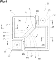
FIG. 4 is a plan view of the light detecting element ofFIG. 3 .FIG. 5 is a cross-sectional view of the light detecting element ofFIG. 3 . -
FIG. 6 is a diagram illustrating a principle of an optical resonance structure. -
FIG. 7 is a plan view of a light detecting element of a modified example. -
FIG. 8 is a cross-sectional view of the light detecting element of the modified example. -
FIG. 9 is a cross-sectional view of the light detecting element of the modified example. -
FIG. 10 is a cross-sectional view of the light detecting element of the modified example. -
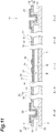
FIG. 11 is a cross-sectional view of the light detecting element of the modified example. -
FIG. 12 is a cross-sectional view of the light detecting element of the modified example. - Hereinafter, a preferred embodiment of the invention will be described in detail with reference to the drawings. Additionally, the same reference numerals will be given to the same or equivalent parts in the drawings and a repetitive description thereof will be omitted.
- A
light detector 1 illustrated inFIG. 1 detects light by using a function of a bolometer. The light is, for example, infrared light. When the light is infrared light, thelight detector 1 is used in an infrared imager, thermography, and the like. As illustrated inFIG. 1 , thelight detector 1 includes asubstrate 2, apixel unit 3, and a signalprocessing circuit unit 4. Thesubstrate 2 is, for example, a Si substrate. The thickness of thesubstrate 2 is, for example, about several hundred µm. Thepixel unit 3 and the signalprocessing circuit unit 4 are formed on thesubstrate 2 and are electrically connected to each other. Additionally, the signalprocessing circuit unit 4 may be formed inside thesubstrate 2. - As illustrated in
FIG. 2 , thepixel unit 3 includes a plurality of light detectingelements 10. The plurality of light detectingelements 10 are arranged in a two-dimensional matrix shape. As illustrated inFIG. 3 , thelight detecting element 10 includes the substrate 2 (exactly a part of the substrate 2), alight reflection layer 5, a pair of electrode plugs 11 and 12, and amembrane 20. - The
light reflection layer 5 is formed on asurface 2a of thesubstrate 2. Thelight reflection layer 5 is opposite to alight absorption layer 34 to be described later and constitutes an optical resonance structure along with thelight absorption layer 34. The thickness of thelight reflection layer 5 is, for example, about several hundreds of nm. The material of thelight reflection layer 5 is, for example, a metal material (for example, A1 or the like) having large reflectivity with respect to light (for example, infrared light). - The pair of electrode plugs 11 and 12 is formed on the
surface 2a of thesubstrate 2. Each of theelectrode plugs electrode plugs electrode plugs membrane 20 on thesurface 2a of thesubstrate 2 so that a space S is formed between thesurface 2a of thesubstrate 2 and themembrane 20. Themembrane 20 is disposed in substantially parallel to thesurface 2a of thesubstrate 2. A distance between themembrane 20 and thesurface 2a of thesubstrate 2 is, for example, about several µm. - As illustrated in
FIGS. 3 and4 , themembrane 20 includes alight receiving portion 21, a pair ofelectrode portions beam portions light receiving portion 21 spreads to avoid each of the electrode plugs 11 and 12 when viewed from the thickness direction of the substrate 2 (that is, a direction perpendicular to thesurface 2a of the substrate 2). Theelectrode portion 22 is disposed on theelectrode plug 11. Theelectrode portion 23 is disposed on theelectrode plug 12. Thebeam portion 24 extends along the outer edge of thelight receiving portion 21 at one side of thelight receiving portion 21. Thebeam portion 25 extends along the outer edge of thelight receiving portion 21 at the other side of thelight receiving portion 21. One end of thebeam portion 24 is connected to theelectrode portion 22 and the other end of thebeam portion 24 is connected to thelight receiving portion 21 at a position in the vicinity of theelectrode portion 23. One end of thebeam portion 25 is connected to theelectrode portion 23 and the other end of thebeam portion 25 is connected to thelight receiving portion 21 at a position in the vicinity of theelectrode portion 22. Themembrane 20 has, for example, a rectangular shape when viewed from the thickness direction of thesubstrate 2. The pair ofelectrode portions membrane 20. - The
light receiving portion 21, the pair ofelectrode portions beam portions Slits 20a are formed in series between the light receivingportion 21 and theelectrode portion 22 and between the light receivingportion 21 and thebeam portion 24.Slits 20b are formed in series between the light receivingportion 21 and theelectrode portion 23 and between the light receivingportion 21 and thebeam portion 25. The width of each of thebeam portions beam portions slits -
FIG. 5 is a cross-sectional view of thelight detecting element 10. The I-I, II-II, III-III, IV-IV, and V-V ofFIG. 5 are cross-sectional views taken along the lines I-I, II-II, III-III, IV-IV, and V-V ofFIG. 4 . As illustrated inFIG. 5 , themembrane 20 includes afirst wiring layer 31, asecond wiring layer 32, aresistance layer 33, alight absorption layer 34, and aseparation layer 35. - As illustrated in
FIGS. 4 and5 , When viewed from the thickness direction of thesubstrate 2, thefirst wiring layer 31 and thesecond wiring layer 32 are opposite each other with the gap G interposed therebetween in thelight receiving portion 21. The gap G extends along the line L. The line L extends in, for example, a linear shape to connect theelectrode portion 22 and theelectrode portion 23 when viewed from the thickness direction of thesubstrate 2. Thefirst wiring layer 31 and thesecond wiring layer 32 are formed in an elongated shape in a direction along the line L in thelight receiving portion 21. That is, the length of each of thefirst wiring layer 31 and thesecond wiring layer 32 in a direction along the line L in thelight receiving portion 21 is larger than the width of each of thefirst wiring layer 31 and thesecond wiring layer 32 in a direction perpendicular to the line L when viewed from the thickness direction of thesubstrate 2. - Specifically, the
first wiring layer 31 includes afirst edge portion 31a and asecond edge portion 31b in thelight receiving portion 21. When viewed from the thickness direction of thesubstrate 2, each of thefirst edge portion 31a and thesecond edge portion 31b extends along the line L. Thesecond wiring layer 32 includes athird edge portion 32a and afourth edge portion 32b in thelight receiving portion 21. When viewed from the thickness direction of thesubstrate 2, each of thethird edge portion 32a and thefourth edge portion 32b extends along the line L. When viewed from the thickness direction of thesubstrate 2, thefirst edge portion 31a and thethird edge portion 32a are opposite each other with the line L interposed therebetween. That is, when viewed from the thickness direction of thesubstrate 2, the gap G is defined by thefirst edge portion 31a and thethird edge portion 32a. - When viewed from the thickness direction of the
substrate 2, the length of each of thefirst wiring layer 31 and thesecond wiring layer 32 in a direction along the line L of thelight receiving portion 21 is, for example, several tens to several hundreds of µm. When viewed from the thickness direction of thesubstrate 2, the width of each of thefirst wiring layer 31 and thesecond wiring layer 32 in a direction perpendicular to the line L is, for example, about several µm. When viewed from the thickness direction of thesubstrate 2, the width of the gap G in a direction perpendicular to the line L is, for example, about several µm. The thickness of each of thefirst wiring layer 31 and thesecond wiring layer 32 is, for example, about several tens to several hundreds of nm. - The
first wiring layer 31 extends from thelight receiving portion 21 to theelectrode portion 22 through thebeam portion 24. Thefirst wiring layer 31 is formed on theelectrode plug 11 in theelectrode portion 22. Thefirst wiring layer 31 is electrically connected to theelectrode plug 11. Thesecond wiring layer 32 extends from thelight receiving portion 21 to theelectrode portion 23 through thebeam portion 25. Thesecond wiring layer 32 is formed on theelectrode plug 12 in theelectrode portion 23. Thesecond wiring layer 32 is electrically connected to theelectrode plug 12. The material of each of thefirst wiring layer 31 and thesecond wiring layer 32 is, for example, a metal material such as Ti. - The
resistance layer 33 is formed to cover thefirst wiring layer 31 and thesecond wiring layer 32 from the side opposite to thesubstrate 2 in thelight receiving portion 21. Theresistance layer 33 covers the surface opposite to thesubstrate 2 of each of thefirst wiring layer 31 and thesecond wiring layer 32 in thelight receiving portion 21 and the side surface of each of thefirst wiring layer 31 and thesecond wiring layer 32. That is, theresistance layer 33 is disposed in the gap G. Theresistance layer 33 is formed on the surface opposite to thesubstrate 2 of thefirst wiring layer 31 and thesecond wiring layer 32 in theelectrode portions beam portions resistance layer 33 is electrically connected to each of thefirst wiring layer 31 and thesecond wiring layer 32. The thickness of theresistance layer 33 is, for example, about several tens to several hundreds of nm. Theresistance layer 33 has an electric resistance depending on a temperature. The material of theresistance layer 33 is, for example, a material having a large change in electrical resistivity due to a temperature change such as amorphous silicon (a-Si). - The
light absorption layer 34 is opposite to thesurface 2a of thesubstrate 2 of thelight receiving portion 21. Thelight absorption layer 34 is disposed at the side opposite to thesubstrate 2 with respect to theresistance layer 33. Thelight absorption layer 34 spreads in the substantially entire region of thelight receiving portion 21 when viewed from the thickness direction of thesubstrate 2. The thickness of thelight absorption layer 34 is, for example, about several tens of nm. The material of thelight absorption layer 34 is, for example, WSi2 or Ti. - The
separation layer 35 is disposed between thefirst wiring layer 31 and thelight absorption layer 34, and thesecond wiring layer 32 and theabsorption layer 34. Specifically, theseparation layer 35 is formed on the surface opposite to thesubstrate 2 of theresistance layer 33 in thelight receiving portion 21, thebeam portions electrode portions light absorption layer 34 is formed on the surface at the side opposite to thesubstrate 2 in theseparation layer 35 of thelight receiving portion 21. The thickness of theseparation layer 35 is, for example, about several hundreds of nm. The thickness of theseparation layer 35 is larger than the thickness of each of thefirst wiring layer 31, thesecond wiring layer 32, theresistance layer 33, and thelight absorption layer 34. The material of theseparation layer 35 is, for example, a silicon nitride film (SiN) or the like. - When viewed from the thickness direction of the
substrate 2, thelight absorption layer 34 includes thefirst region 34a and thesecond region 34b. Thefirst region 34a spreads to the side opposite to thesecond wiring layer 32 with respect to thefirst wiring layer 31 when viewed from the thickness direction of thesubstrate 2. Thesecond region 34b spreads to the side opposite to thefirst wiring layer 31 with respect to thesecond wiring layer 32 when viewed from the thickness direction of thesubstrate 2. When viewed from the thickness direction of thesubstrate 2, the total area of thefirst wiring layer 31 and thesecond wiring layer 32 is smaller than each area of thefirst region 34a and thesecond region 34b. - Additionally, the
first region 34a and thesecond region 34b of thelight absorption layer 34 are formed on theresistance layer 33 with theseparation layer 35 interposed therebetween. Further, theresistance layer 33 and theseparation layer 35 are respectively formed continuously over thefirst region 34a and thesecond region 34b. - In the
light detector 1 with the above-described configuration, light is detected as below. First, when incident light is incident to thelight receiving portion 21, heat is generated in thelight absorption layer 34 constituting an optical resonance structure to be described later. At this time, thelight receiving portion 21 and thesubstrate 2 are thermally separated from each other by a space S. Further, thelight receiving portion 21, theelectrode portion 22, and thebeam portion 24 are thermally separated from one another by theslit 20a. Further, thelight receiving portion 21, theelectrode portion 23, and thebeam portion 25 are thermally separated from one another by theslit 20b. For this reason, heat generated in thelight absorption layer 34 is suppressed from escaping to thesubstrate 2 through thebeam portions electrode portions - The heat generated in the
light absorption layer 34 is transmitted to theresistance layer 33 through theseparation layer 35. Then, theresistance layer 33 increases in temperature and electric resistance due to the heat. Such a change in electric resistance is transmitted to the signalprocessing circuit unit 4 as a signal through the first and second wiring layers 31 and 32 and the electrode plugs 11 and 12 electrically connected to theresistance layer 33. Then, in the signalprocessing circuit unit 4, a change in electric resistance of theresistance layer 33 is converted into a change in voltage or current and light is detected on the basis of a change in voltage or current. - Next, the optical resonance structure will be described in detail. As illustrated in
FIG. 6 , a part of incident light A (having a wavelength λ) incident to thelight absorption layer 34 is reflected as reflected light B1 by thelight absorption layer 34 and the other part of the incident light A is transmitted through thelight absorption layer 34. The other part of the incident light A transmitted through thelight absorption layer 34 is reflected as reflected light B2 by thelight reflection layer 5. Then, the reflected light B1 and the reflected light B2 interfere with each other to disappear on the reflection surface of thelight absorption layer 34. Accordingly, the incident light A is absorbed on the reflection surface of thelight absorption layer 34. Then, heat is generated in thelight absorption layer 34 due to the energy of the absorbed incident light A. - The absorption rate of the incident light A can be determined by a sheet resistance of the
light absorption layer 34 and an optical distance t between thelight absorption layer 34 and thelight reflection layer 5. The thickness of thelight absorption layer 34 is set to about 16 nm (when the material of thelight absorption layer 34 is WSi2) so that the sheet resistance becomes a vacuum impedance (377 Ω/sq). Accordingly, the amplitude of the reflected light B1 reflected by thelight absorption layer 34 matches the amplitude of the reflected light B2 reflected by thelight reflection layer 5. For this reason, the reflected light B1 and the reflected light B2 efficiently interfere with each other to disappear on the reflection surface of thelight absorption layer 34. Thus, the absorption rate of the incident light A is improved. - Further, the optical distance t is set so that t = (2m - 1)λ/4 (m = 1, 2, 3, ...). Accordingly, the phases of the reflected light B1 and the reflected light B2 are shifted by 180°. For this reason, the reflected light B1 and the reflected light B2 efficiently interfere with each other to disappear on the reflection surface of the
light absorption layer 34. Thus, the absorption rate of the incident light A is improved. In this way, thelight reflection layer 5 constitutes an optical resonance structure along with thelight absorption layer 34. When viewed from the thickness direction of thesubstrate 2, the incident light A is efficiently absorbed as the area of the overlapping portion between thelight reflection layer 5 and thelight absorption layer 34 becomes wider. - As described above, in the
light detector 1 of the embodiment, thefirst region 34a of thelight absorption layer 34 spreads to the side opposite to thesecond wiring layer 32 with respect to thefirst wiring layer 31 and thesecond region 34b of thelight absorption layer 34 spreads to the side opposite to thefirst wiring layer 31 with respect to thesecond wiring layer 32 when viewed from the thickness direction of thesubstrate 2. That is, thefirst region 34a of thelight absorption layer 34 does not overlap thefirst wiring layer 31 and thesecond region 34b of thelight absorption layer 34 does not overlap thesecond wiring layer 32 when viewed from the thickness direction of thesubstrate 2. Accordingly, sufficient light absorption in thefirst region 34a and thesecond region 34b of thelight absorption layer 34 is realized. Further, theseparation layer 35 is disposed between thefirst wiring layer 31 and thelight absorption layer 34, and thesecond wiring layer 32 and theabsorption layer 34. Accordingly, since the heat generated in thelight absorption layer 34 is suppressed from escaping to thesubstrate 2 through thefirst wiring layer 31 and thesecond wiring layer 32, the heat is sufficiently transmitted to theresistance layer 33 through theseparation layer 35. As described above, according to thelight detector 1, sensitivity can be improved. The sensitivity means an ability of detecting light by thelight detector 1. For example, it is understood that the sensitivity of thelight detector 1 is high when thelight detector 1 can detect weak light and the sensitivity of thelight detector 1 is low when thelight detector 1 cannot detect strong light. - Further, since the
separation layer 35 is disposed between thefirst wiring layer 31 and thelight absorption layer 34, and thesecond wiring layer 32 and theabsorption layer 34, themembrane 20 is difficult to warp. Further, each of thefirst wiring layer 31 and thesecond wiring layer 32 is formed in thelight receiving portion 21 to cross thelight receiving portion 21. Accordingly, since themembrane 20 is reliably supported by thefirst wiring layer 31 and thesecond wiring layer 32, it is possible to suppress the distortion and deformation of theresistance layer 33 between thefirst wiring layer 31 and thesecond wiring layer 32. - Further, in the
light detector 1, thelight reflection layer 5 is disposed on thesurface 2a of thesubstrate 2 and constitutes an optical resonance structure along with thelight absorption layer 34. According to this configuration, it is possible to realize light absorption in a wavelength region corresponding to a distance between thelight absorption layer 34 and thelight reflection layer 5. - Further, in the
light detector 1, the total area of thefirst wiring layer 31 and thesecond wiring layer 32 is smaller than each area of thefirst region 34a and thesecond region 34b when viewed from the thickness direction of thesubstrate 2. According to this configuration, since more sufficient light absorption in thefirst region 34a and thesecond region 34b of thelight absorption layer 34 is realized and the heat generated in thelight absorption layer 34 is further suppressed from escaping to thesubstrate 2 through thefirst wiring layer 31 and thesecond wiring layer 32, sensitivity can be further improved. - Further, in the
light detector 1, the length of each of thefirst wiring layer 31 and thesecond wiring layer 32 in a direction along the line L is larger than the width of each of thefirst wiring layer 31 and thesecond wiring layer 32 in a direction perpendicular to the line L when viewed from the thickness direction of thesubstrate 2. According to this configuration, since the gap G is lengthened, sensitivity can be further improved. - Further, in the
light detector 1, the thickness of theseparation layer 35 is larger than the thickness of each of thefirst wiring layer 31, thesecond wiring layer 32, theresistance layer 33, and thelight absorption layer 34. According to this configuration, since the heat generated in thelight absorption layer 34 is further suppressed from escaping to thesubstrate 2 through thefirst wiring layer 31 and thesecond wiring layer 32, sensitivity can be further improved. Further, according to this configuration, it is possible to improve the strength of themembrane 20 and to suppress the deformation of themembrane 20. - Further, in the
light detector 1, thefirst region 34a and thesecond region 34b of thelight absorption layer 34 are formed on theresistance layer 33 with theseparation layer 35 interposed therebetween. Further, theresistance layer 33 and theseparation layer 35 are respectively formed continuously over thefirst region 34a and thesecond region 34b. According to this configuration, it is possible to suppress the deformation and warpage of themembrane 20 and to simplify the process of manufacturing thelight detector 1. - Although the embodiment of the invention has been described above, an aspect of the invention is not limited to the above-described embodiment.
- In the above-described embodiment, an example in which the
membrane 20 has, for example, a rectangular shape when viewed from the thickness direction of thesubstrate 2 has been described, but the invention is not limited thereto. Themembrane 20 may have, for example, various shapes such as a circular shape when viewed from the thickness direction of thesubstrate 2. - Further, an example is illustrated in which the positions of the
first wiring layer 31 and thesecond wiring layer 32 in the thickness direction of thesubstrate 2 match each other, but the positions of thefirst wiring layer 31 and thesecond wiring layer 32 in the thickness direction of thesubstrate 2 may not match each other. - Further, an example in which the line L extends in a linear shape to connect, for example, the
electrode portion 22 and theelectrode portion 23 when viewed from the thickness direction of thesubstrate 2 has been described, but the invention is not limited thereto. As illustrated inFIG. 7 , the line L may extend, for example, in a meandering shape having a curved portion when viewed from the thickness direction of thesubstrate 2. Accordingly, since the gap G is lengthened as compared with a case in which the line L is linear, sensitivity can be improved. Additionally, when the line L has a curved portion, a direction perpendicular to the line L means a direction perpendicular to a tangent line at each position of the line L. Directions perpendicular to the line L are different at each position of the curved portion, respectively. - Further, the
resistance layer 33 may not be formed in, for example, a region corresponding to theelectrode portions beam portions first region 34a and a region corresponding to thesecond region 34b. - Further, the
separation layer 35 may not be disposed in, for example, a region corresponding to theelectrode portions beam portions first region 34a and a region corresponding to thesecond region 34b. Further, the thickness of theseparation layer 35 may be equal to or smaller than the thickness of each of thefirst wiring layer 31, thesecond wiring layer 32, theresistance layer 33, and thelight absorption layer 34. Further, the material of theseparation layer 35 may be the same as that of the resistance layer 33 (seeFIG. 9 ). - Further, the total area of the
first wiring layer 31 and thesecond wiring layer 32 may be smaller than the total area of thefirst region 34a and thesecond region 34b when viewed from the thickness direction of thesubstrate 2. According to this configuration, as described above, since more sufficient light absorption in thefirst region 34a and thesecond region 34b of thelight absorption layer 34 is realized and the heat generated in thelight absorption layer 34 is further suppressed from escaping to thesubstrate 2 through thefirst wiring layer 31 and thesecond wiring layer 32, sensitivity can be further improved. - Further, as illustrated in
FIG. 8 , theseparation layer 35 and thelight absorption layer 34 may be formed on the side of thesubstrate 2 in thefirst wiring layer 31 and thesecond wiring layer 32. Specifically, theseparation layer 35 is formed on the electrode plugs 11 and 12. Thefirst wiring layer 31, thesecond wiring layer 32, and theresistance layer 33 are formed on the surface opposite to thesubstrate 2 in theseparation layer 35. Thelight absorption layer 34 is formed on the surface at the side of thesubstrate 2 in theseparation layer 35. Accordingly, thelight absorption layer 34 and thelight reflection layer 5 directly face each other with the space S interposed therebetween. For this reason, since it is easy to adjust the optical distance t, it is possible to more reliably absorb light by the optical resonance structure. Additionally, also in this case, thefirst wiring layer 31 is electrically connected to theelectrode plug 11. Thesecond wiring layer 32 is electrically connected to theelectrode plug 12. - Further, as illustrated in
FIG. 9 , when theresistance layer 33 is formed between thefirst wiring layer 31 and thelight absorption layer 34, and thesecond wiring layer 32 and theabsorption layer 34, themembrane 20 may not include theseparation layer 35. In this case, theresistance layer 33 serves as both theresistance layer 33 and theseparation layer 35. Accordingly, since the thermal conductance of themembrane 20 is low, the response speed can be improved. The response speed indicates a change rate of the temperature of themembrane 20 with respect to time when the light (for example, the amount of light) incident to thelight receiving portion 21 changes. For example, it is understood that the response speed is fast when the time taken until the temperature of themembrane 20 rises to a predetermined stable temperature is short in a case in which the amount of light incident to thelight receiving portion 21 increases and the response speed is slow when the time is long in that case. Further, accordingly, since the element resistance of themembrane 20 is low, noise can be reduced. - Further, as illustrated in
FIG. 10 , theresistance layer 33 may be formed on the side of thesubstrate 2 in thefirst wiring layer 31 and thesecond wiring layer 32. In this case, theresistance layer 33 is not disposed at the gap G. Additionally, also in this case, thefirst wiring layer 31 is electrically connected to theelectrode plug 11. Thesecond wiring layer 32 is electrically connected to theelectrode plug 12. - Further, as illustrated in
FIG. 11 , theresistance layer 33, theseparation layer 35, and thelight absorption layer 34 may be formed on the side of thesubstrate 2 in thefirst wiring layer 31 and thesecond wiring layer 32. Specifically, theseparation layer 35 is formed on the electrode plugs 11 and 12. Theresistance layer 33 is formed on the surface opposite to thesubstrate 2 in theseparation layer 35. Thefirst wiring layer 31 and thesecond wiring layer 32 are formed on the surface opposite to thesubstrate 2 in theresistance layer 33. Thelight absorption layer 34 is formed on the surface at the side of thesubstrate 2 in theseparation layer 35. Additionally, also in this case, thefirst wiring layer 31 is electrically connected to theelectrode plug 11. Thesecond wiring layer 32 is electrically connected to theelectrode plug 12. - Further, as illustrated in
FIG. 12 , themembrane 20 may not include theseparation layer 35 when theresistance layer 33 is formed between thefirst wiring layer 31 and thelight absorption layer 34, and thesecond wiring layer 32 and theabsorption layer 34, also in a case in which theresistance layer 33 and thelight absorption layer 34 are formed on the side of thesubstrate 2 in thefirst wiring layer 31 and thesecond wiring layer 32. That is, also in this case, theresistance layer 33 serves as both theresistance layer 33 and theseparation layer 35. Additionally, also in this case, thefirst wiring layer 31 is electrically connected to theelectrode plug 11. Thesecond wiring layer 32 is electrically connected to theelectrode plug 12. - Further, in the above-described configurations, the material of the
light absorption layer 34 may be, for example, a material having a large absorption rate with respect to light such as black resin. Additionally, in this case, the optical resonance structure is not provided and light is directly absorbed by thelight absorption layer 34. Accordingly, as described above, the optical distance t may not be accurately adjusted. Additionally, it is desirable that thelight detecting element 10 include thelight reflection layer 5 even when the optical resonance structure is not provided. The reason is as below. When a part of the incident light A incident to thelight absorption layer 34 is not absorbed by thelight absorption layer 34 and is transmitted through themembrane 20, the incident light A transmitted through themembrane 20 is reflected by thelight reflection layer 5 and is again incident to thelight absorption layer 34. The incident light A which is incident to thelight absorption layer 34 again is absorbed by thelight absorption layer 34 to become heat. Accordingly, the absorption rate of the light is improved. Further, when theseparation layer 35 is disposed between thelight absorption layer 34 and theresistance layer 33 in a case in which the material of thelight absorption layer 34 is black resin, thelight absorption layer 34 contacts theresistance layer 33 so that an influence on the characteristic of theresistance layer 33 is suppressed. - Further, in the above-described configurations, the
separation layer 35 may be further formed on the surface at the side of thesubstrate 2 in themembrane 20. Accordingly, it is possible to stabilize theresistance layer 33 and to make themembrane 20 harder to warp. - Further, each of the
first wiring layer 31, thesecond wiring layer 32, theresistance layer 33, thelight absorption layer 34, and theseparation layer 35 can be formed with various materials and thicknesses. When each of thefirst wiring layer 31, thesecond wiring layer 32, theresistance layer 33, and theseparation layer 35 is formed with optimal materials and thicknesses, the sensitivity can be easily improved and the strength of themembrane 20 can be improved. Further, it is possible to improve both sensitivity and response speed by selecting an optimal material for each of thefirst wiring layer 31, thesecond wiring layer 32, and thelight absorption layer 34 as compared with a conventional structure (for example, see Patent Literature 1) using the wiring layer as the light absorption layer. - Further, the
pixel unit 3 may constituted by onelight detecting element 10. - 1: light detector, 2: substrate, 2a: surface, 20: membrane, 31: first wiring layer, 32: second wiring layer, 33: resistance layer, 34: light absorption layer, 34a: first region, 34b: second region, 35: separation layer, 5: light reflection layer, L: line, S: space, G: gap.
Claims (6)
- A light detector comprising:a substrate; anda membrane which is supported on a surface of the substrate so that a space is formed between the surface of the substrate and the membrane,wherein the membrane includes a first wiring layer and a second wiring layer which are opposite each other with a gap extending along a line interposed therebetween, a resistance layer which is electrically connected to each of the first wiring layer and the second wiring layer and has an electric resistance depending on a temperature, a light absorption layer which is opposite to the surface of the substrate, and a separation layer which is disposed between the first wiring layer and the light absorption layer, and the second wiring layer and the absorption layer, andwherein the light absorption layer includes a first region which spreads to the side opposite to the second wiring layer with respect to the first wiring layer when viewed from the thickness direction of the substrate and a second region which spreads to the side opposite to the first wiring layer with respect to the second wiring layer when viewed from the thickness direction of the substrate.
- The light detector according to claim 1, further comprising:
a light reflection layer which is disposed on the surface of the substrate and constitutes an optical resonance structure along with the light absorption layer. - The light detector according to claim 1 or 2,
wherein a total area of the first wiring layer and the second wiring layer is smaller than a total area of the first region and the second region when viewed from the thickness direction of the substrate. - The light detector according to any one of claims 1 to 3,
wherein a total area of the first wiring layer and the second wiring layer is smaller than a area of each of the first region and the second region when viewed from the thickness direction of the substrate. - The light detector according to any one of claims 1 to 4,
wherein a length of each of the first wiring layer and the second wiring layer in a direction along the line is larger than a width of each of the first wiring layer and the second wiring layer in a direction perpendicular to the line when viewed from the thickness direction of the substrate. - The light detector according to any one of claims 1 to 5,
wherein a thickness of the separation layer is larger than a thickness of each of the first wiring layer, the second wiring layer, the resistance layer, and the light absorption layer.
Applications Claiming Priority (2)
| Application Number | Priority Date | Filing Date | Title |
|---|---|---|---|
| JP2016242467A JP6726087B2 (en) | 2016-12-14 | 2016-12-14 | Photo detector |
| PCT/JP2017/043174 WO2018110310A1 (en) | 2016-12-14 | 2017-11-30 | Light detector |
Publications (3)
| Publication Number | Publication Date |
|---|---|
| EP3557203A1 true EP3557203A1 (en) | 2019-10-23 |
| EP3557203A4 EP3557203A4 (en) | 2020-08-19 |
| EP3557203B1 EP3557203B1 (en) | 2023-06-07 |
Family
ID=62559799
Family Applications (1)
| Application Number | Title | Priority Date | Filing Date |
|---|---|---|---|
| EP17882029.6A Active EP3557203B1 (en) | 2016-12-14 | 2017-11-30 | Light detector |
Country Status (6)
| Country | Link |
|---|---|
| US (1) | US10852194B2 (en) |
| EP (1) | EP3557203B1 (en) |
| JP (1) | JP6726087B2 (en) |
| CN (1) | CN110023724B (en) |
| TW (1) | TW201829989A (en) |
| WO (1) | WO2018110310A1 (en) |
Families Citing this family (2)
| Publication number | Priority date | Publication date | Assignee | Title |
|---|---|---|---|---|
| EP3746813A4 (en) | 2018-02-03 | 2021-08-11 | Shenzhen Xpectvision Technology Co., Ltd. | RADIATION DETECTOR RECOVERY METHODS |
| JP7309138B2 (en) * | 2020-12-25 | 2023-07-18 | 国立大学法人横浜国立大学 | Gas sensor with infrared absorber and infrared absorber |
Family Cites Families (21)
| Publication number | Priority date | Publication date | Assignee | Title |
|---|---|---|---|---|
| US5021663B1 (en) * | 1988-08-12 | 1997-07-01 | Texas Instruments Inc | Infrared detector |
| DE69313337T2 (en) * | 1992-04-17 | 1998-01-02 | Terumo Corp | Infrared sensor and method for its manufacture |
| FR2773215B1 (en) * | 1997-12-31 | 2000-01-28 | Commissariat Energie Atomique | BOLOMETRIC THERMAL DETECTOR |
| FR2796148B1 (en) | 1999-07-08 | 2001-11-23 | Commissariat Energie Atomique | BOLOMETRIC DETECTOR WITH INTERMEDIATE ELECTRICAL INSULATION AND MANUFACTURING METHOD THEREOF |
| JP2001272271A (en) * | 2000-01-17 | 2001-10-05 | Mitsubishi Electric Corp | Infrared sensor |
| JP2002107224A (en) * | 2000-09-29 | 2002-04-10 | Toshiba Corp | Infrared sensor and method of manufacturing the same |
| JP3691395B2 (en) * | 2001-01-19 | 2005-09-07 | シャープ株式会社 | Thermal infrared detection element, method for manufacturing the same, and imaging apparatus including the thermal infrared detection element |
| JP2003294523A (en) * | 2002-04-03 | 2003-10-15 | Mitsubishi Electric Corp | Infrared detector, method of manufacturing the same, and infrared solid-state imaging device |
| JP2004151059A (en) * | 2002-11-01 | 2004-05-27 | Mitsubishi Electric Corp | Infrared detector |
| JP3862080B2 (en) * | 2002-11-01 | 2006-12-27 | 防衛庁技術研究本部長 | Method for manufacturing thermal infrared detector |
| US6891161B2 (en) * | 2003-01-17 | 2005-05-10 | Drs Sensors & Targeting Systems, Inc. | Pixel structure and an associated method of fabricating the same |
| FR2861172B1 (en) * | 2003-10-15 | 2006-06-02 | Ulis | BOLOMETRIC DETECTOR, INFRARED DETECTION DEVICE USING SUCH A BOLOMETRIC DETECTOR AND METHOD FOR MANUFACTURING SAME |
| KR100925214B1 (en) * | 2007-11-29 | 2009-11-06 | 한국전자통신연구원 | Volometer and its manufacturing method |
| WO2011013197A1 (en) * | 2009-07-28 | 2011-02-03 | 株式会社 東芝 | Infrared imaging device |
| KR101182406B1 (en) | 2009-08-21 | 2012-09-13 | 한국전자통신연구원 | The Infrared detection sensor and manufacturing method thereof |
| KR20120059019A (en) * | 2010-11-30 | 2012-06-08 | 삼성전자주식회사 | Thermal image sensor with chacogenide material and method of fabrication |
| JP2012194080A (en) * | 2011-03-17 | 2012-10-11 | Nec Corp | Bolometer type thz wave detector |
| US9368658B2 (en) * | 2012-08-31 | 2016-06-14 | Robert Bosch Gmbh | Serpentine IR sensor |
| JP6142618B2 (en) * | 2013-03-28 | 2017-06-07 | Tdk株式会社 | Infrared sensor |
| US9404804B1 (en) * | 2015-04-02 | 2016-08-02 | Palo Alto Research Center Incorporated | Thermal sensor with infrared absorption membrane including metamaterial structure |
| CN105737993B (en) * | 2016-02-02 | 2019-04-26 | 烟台睿创微纳技术股份有限公司 | A tunable microbolometer pixel structure and pixel array |
-
2016
- 2016-12-14 JP JP2016242467A patent/JP6726087B2/en active Active
-
2017
- 2017-11-30 EP EP17882029.6A patent/EP3557203B1/en active Active
- 2017-11-30 US US16/468,046 patent/US10852194B2/en active Active
- 2017-11-30 CN CN201780073822.4A patent/CN110023724B/en active Active
- 2017-11-30 WO PCT/JP2017/043174 patent/WO2018110310A1/en not_active Ceased
- 2017-12-08 TW TW106143163A patent/TW201829989A/en unknown
Also Published As
| Publication number | Publication date |
|---|---|
| WO2018110310A1 (en) | 2018-06-21 |
| CN110023724A (en) | 2019-07-16 |
| EP3557203A4 (en) | 2020-08-19 |
| CN110023724B (en) | 2021-05-18 |
| TW201829989A (en) | 2018-08-16 |
| JP6726087B2 (en) | 2020-07-22 |
| EP3557203B1 (en) | 2023-06-07 |
| JP2018096878A (en) | 2018-06-21 |
| US10852194B2 (en) | 2020-12-01 |
| US20200072676A1 (en) | 2020-03-05 |
Similar Documents
| Publication | Publication Date | Title |
|---|---|---|
| JP5684487B2 (en) | Bolometer detector for detecting electromagnetic radiation in the infrared to terahertz frequency band, and array detection apparatus having such a detector | |
| US9217674B2 (en) | Bolometric detector of an electromagnetic radiation in the terahertz range and array detection device comprising such detectors | |
| EP2375228B1 (en) | Optical sensor | |
| EP3025132B1 (en) | An apparatus for sensing | |
| EP3557202A1 (en) | Light detector | |
| US10852194B2 (en) | Light detector | |
| RU2004129916A (en) | BOLOMETRIC DETECTOR, DEVICE FOR DETECTING INFRARED RADIATION USING SUCH A BOLOMETRIC DETECTOR AND METHOD FOR PRODUCING THIS DETECTOR | |
| US20200249084A1 (en) | Light detector | |
| JP6292297B2 (en) | Terahertz wave detector | |
| EP3667269B1 (en) | Light detector | |
| WO2017077996A1 (en) | Bolometer type terahertz wave detector | |
| WO2016132616A1 (en) | Infrared detection device | |
| US20250347564A1 (en) | Bolometer array, bolometer array unit, and light detection method | |
| JPH0733979B2 (en) | Temperature sensor | |
| JP2013253896A (en) | Photo detector, camera, and electronic apparatus | |
| JPH0915039A (en) | Infrared detector and infrared detector array |
Legal Events
| Date | Code | Title | Description |
|---|---|---|---|
| STAA | Information on the status of an ep patent application or granted ep patent |
Free format text: STATUS: THE INTERNATIONAL PUBLICATION HAS BEEN MADE |
|
| PUAI | Public reference made under article 153(3) epc to a published international application that has entered the european phase |
Free format text: ORIGINAL CODE: 0009012 |
|
| STAA | Information on the status of an ep patent application or granted ep patent |
Free format text: STATUS: REQUEST FOR EXAMINATION WAS MADE |
|
| 17P | Request for examination filed |
Effective date: 20190423 |
|
| AK | Designated contracting states |
Kind code of ref document: A1 Designated state(s): AL AT BE BG CH CY CZ DE DK EE ES FI FR GB GR HR HU IE IS IT LI LT LU LV MC MK MT NL NO PL PT RO RS SE SI SK SM TR |
|
| AX | Request for extension of the european patent |
Extension state: BA ME |
|
| DAV | Request for validation of the european patent (deleted) | ||
| DAX | Request for extension of the european patent (deleted) | ||
| A4 | Supplementary search report drawn up and despatched |
Effective date: 20200720 |
|
| RIC1 | Information provided on ipc code assigned before grant |
Ipc: G01J 1/02 20060101AFI20200714BHEP Ipc: G01J 5/20 20060101ALI20200714BHEP Ipc: H01L 27/144 20060101ALI20200714BHEP Ipc: H01L 27/146 20060101ALI20200714BHEP Ipc: H01L 31/0248 20060101ALI20200714BHEP |
|
| GRAP | Despatch of communication of intention to grant a patent |
Free format text: ORIGINAL CODE: EPIDOSNIGR1 |
|
| STAA | Information on the status of an ep patent application or granted ep patent |
Free format text: STATUS: GRANT OF PATENT IS INTENDED |
|
| RIC1 | Information provided on ipc code assigned before grant |
Ipc: G01J 5/02 20060101ALI20220628BHEP Ipc: G01J 5/20 20060101ALI20220628BHEP Ipc: H01L 31/0248 20060101ALI20220628BHEP Ipc: H01L 27/146 20060101ALI20220628BHEP Ipc: H01L 27/144 20060101ALI20220628BHEP Ipc: G01J 1/02 20060101AFI20220628BHEP |
|
| INTG | Intention to grant announced |
Effective date: 20220718 |
|
| GRAJ | Information related to disapproval of communication of intention to grant by the applicant or resumption of examination proceedings by the epo deleted |
Free format text: ORIGINAL CODE: EPIDOSDIGR1 |
|
| STAA | Information on the status of an ep patent application or granted ep patent |
Free format text: STATUS: REQUEST FOR EXAMINATION WAS MADE |
|
| INTC | Intention to grant announced (deleted) | ||
| GRAP | Despatch of communication of intention to grant a patent |
Free format text: ORIGINAL CODE: EPIDOSNIGR1 |
|
| STAA | Information on the status of an ep patent application or granted ep patent |
Free format text: STATUS: GRANT OF PATENT IS INTENDED |
|
| INTG | Intention to grant announced |
Effective date: 20230120 |
|
| GRAS | Grant fee paid |
Free format text: ORIGINAL CODE: EPIDOSNIGR3 |
|
| GRAA | (expected) grant |
Free format text: ORIGINAL CODE: 0009210 |
|
| STAA | Information on the status of an ep patent application or granted ep patent |
Free format text: STATUS: THE PATENT HAS BEEN GRANTED |
|
| AK | Designated contracting states |
Kind code of ref document: B1 Designated state(s): AL AT BE BG CH CY CZ DE DK EE ES FI FR GB GR HR HU IE IS IT LI LT LU LV MC MK MT NL NO PL PT RO RS SE SI SK SM TR |
|
| REG | Reference to a national code |
Ref country code: GB Ref legal event code: FG4D |
|
| REG | Reference to a national code |
Ref country code: CH Ref legal event code: EP Ref country code: AT Ref legal event code: REF Ref document number: 1576425 Country of ref document: AT Kind code of ref document: T Effective date: 20230615 |
|
| REG | Reference to a national code |
Ref country code: DE Ref legal event code: R096 Ref document number: 602017070003 Country of ref document: DE |
|
| P01 | Opt-out of the competence of the unified patent court (upc) registered |
Effective date: 20230625 |
|
| REG | Reference to a national code |
Ref country code: LT Ref legal event code: MG9D |
|
| REG | Reference to a national code |
Ref country code: NL Ref legal event code: MP Effective date: 20230607 |
|
| PG25 | Lapsed in a contracting state [announced via postgrant information from national office to epo] |
Ref country code: SE Free format text: LAPSE BECAUSE OF FAILURE TO SUBMIT A TRANSLATION OF THE DESCRIPTION OR TO PAY THE FEE WITHIN THE PRESCRIBED TIME-LIMIT Effective date: 20230607 Ref country code: NO Free format text: LAPSE BECAUSE OF FAILURE TO SUBMIT A TRANSLATION OF THE DESCRIPTION OR TO PAY THE FEE WITHIN THE PRESCRIBED TIME-LIMIT Effective date: 20230907 Ref country code: ES Free format text: LAPSE BECAUSE OF FAILURE TO SUBMIT A TRANSLATION OF THE DESCRIPTION OR TO PAY THE FEE WITHIN THE PRESCRIBED TIME-LIMIT Effective date: 20230607 |
|
| REG | Reference to a national code |
Ref country code: AT Ref legal event code: MK05 Ref document number: 1576425 Country of ref document: AT Kind code of ref document: T Effective date: 20230607 |
|
| PG25 | Lapsed in a contracting state [announced via postgrant information from national office to epo] |
Ref country code: RS Free format text: LAPSE BECAUSE OF FAILURE TO SUBMIT A TRANSLATION OF THE DESCRIPTION OR TO PAY THE FEE WITHIN THE PRESCRIBED TIME-LIMIT Effective date: 20230607 Ref country code: NL Free format text: LAPSE BECAUSE OF FAILURE TO SUBMIT A TRANSLATION OF THE DESCRIPTION OR TO PAY THE FEE WITHIN THE PRESCRIBED TIME-LIMIT Effective date: 20230607 Ref country code: LV Free format text: LAPSE BECAUSE OF FAILURE TO SUBMIT A TRANSLATION OF THE DESCRIPTION OR TO PAY THE FEE WITHIN THE PRESCRIBED TIME-LIMIT Effective date: 20230607 Ref country code: LT Free format text: LAPSE BECAUSE OF FAILURE TO SUBMIT A TRANSLATION OF THE DESCRIPTION OR TO PAY THE FEE WITHIN THE PRESCRIBED TIME-LIMIT Effective date: 20230607 Ref country code: HR Free format text: LAPSE BECAUSE OF FAILURE TO SUBMIT A TRANSLATION OF THE DESCRIPTION OR TO PAY THE FEE WITHIN THE PRESCRIBED TIME-LIMIT Effective date: 20230607 Ref country code: GR Free format text: LAPSE BECAUSE OF FAILURE TO SUBMIT A TRANSLATION OF THE DESCRIPTION OR TO PAY THE FEE WITHIN THE PRESCRIBED TIME-LIMIT Effective date: 20230908 |
|
| PG25 | Lapsed in a contracting state [announced via postgrant information from national office to epo] |
Ref country code: FI Free format text: LAPSE BECAUSE OF FAILURE TO SUBMIT A TRANSLATION OF THE DESCRIPTION OR TO PAY THE FEE WITHIN THE PRESCRIBED TIME-LIMIT Effective date: 20230607 |
|
| PG25 | Lapsed in a contracting state [announced via postgrant information from national office to epo] |
Ref country code: SK Free format text: LAPSE BECAUSE OF FAILURE TO SUBMIT A TRANSLATION OF THE DESCRIPTION OR TO PAY THE FEE WITHIN THE PRESCRIBED TIME-LIMIT Effective date: 20230607 |
|
| PG25 | Lapsed in a contracting state [announced via postgrant information from national office to epo] |
Ref country code: IS Free format text: LAPSE BECAUSE OF FAILURE TO SUBMIT A TRANSLATION OF THE DESCRIPTION OR TO PAY THE FEE WITHIN THE PRESCRIBED TIME-LIMIT Effective date: 20231007 |
|
| PG25 | Lapsed in a contracting state [announced via postgrant information from national office to epo] |
Ref country code: SM Free format text: LAPSE BECAUSE OF FAILURE TO SUBMIT A TRANSLATION OF THE DESCRIPTION OR TO PAY THE FEE WITHIN THE PRESCRIBED TIME-LIMIT Effective date: 20230607 Ref country code: SK Free format text: LAPSE BECAUSE OF FAILURE TO SUBMIT A TRANSLATION OF THE DESCRIPTION OR TO PAY THE FEE WITHIN THE PRESCRIBED TIME-LIMIT Effective date: 20230607 Ref country code: RO Free format text: LAPSE BECAUSE OF FAILURE TO SUBMIT A TRANSLATION OF THE DESCRIPTION OR TO PAY THE FEE WITHIN THE PRESCRIBED TIME-LIMIT Effective date: 20230607 Ref country code: PT Free format text: LAPSE BECAUSE OF FAILURE TO SUBMIT A TRANSLATION OF THE DESCRIPTION OR TO PAY THE FEE WITHIN THE PRESCRIBED TIME-LIMIT Effective date: 20231009 Ref country code: IS Free format text: LAPSE BECAUSE OF FAILURE TO SUBMIT A TRANSLATION OF THE DESCRIPTION OR TO PAY THE FEE WITHIN THE PRESCRIBED TIME-LIMIT Effective date: 20231007 Ref country code: EE Free format text: LAPSE BECAUSE OF FAILURE TO SUBMIT A TRANSLATION OF THE DESCRIPTION OR TO PAY THE FEE WITHIN THE PRESCRIBED TIME-LIMIT Effective date: 20230607 Ref country code: CZ Free format text: LAPSE BECAUSE OF FAILURE TO SUBMIT A TRANSLATION OF THE DESCRIPTION OR TO PAY THE FEE WITHIN THE PRESCRIBED TIME-LIMIT Effective date: 20230607 Ref country code: AT Free format text: LAPSE BECAUSE OF FAILURE TO SUBMIT A TRANSLATION OF THE DESCRIPTION OR TO PAY THE FEE WITHIN THE PRESCRIBED TIME-LIMIT Effective date: 20230607 |
|
| PG25 | Lapsed in a contracting state [announced via postgrant information from national office to epo] |
Ref country code: PL Free format text: LAPSE BECAUSE OF FAILURE TO SUBMIT A TRANSLATION OF THE DESCRIPTION OR TO PAY THE FEE WITHIN THE PRESCRIBED TIME-LIMIT Effective date: 20230607 |
|
| REG | Reference to a national code |
Ref country code: DE Ref legal event code: R097 Ref document number: 602017070003 Country of ref document: DE |
|
| PLBE | No opposition filed within time limit |
Free format text: ORIGINAL CODE: 0009261 |
|
| STAA | Information on the status of an ep patent application or granted ep patent |
Free format text: STATUS: NO OPPOSITION FILED WITHIN TIME LIMIT |
|
| PG25 | Lapsed in a contracting state [announced via postgrant information from national office to epo] |
Ref country code: DK Free format text: LAPSE BECAUSE OF FAILURE TO SUBMIT A TRANSLATION OF THE DESCRIPTION OR TO PAY THE FEE WITHIN THE PRESCRIBED TIME-LIMIT Effective date: 20230607 |
|
| PG25 | Lapsed in a contracting state [announced via postgrant information from national office to epo] |
Ref country code: SI Free format text: LAPSE BECAUSE OF FAILURE TO SUBMIT A TRANSLATION OF THE DESCRIPTION OR TO PAY THE FEE WITHIN THE PRESCRIBED TIME-LIMIT Effective date: 20230607 |
|
| 26N | No opposition filed |
Effective date: 20240308 |
|
| PG25 | Lapsed in a contracting state [announced via postgrant information from national office to epo] |
Ref country code: SI Free format text: LAPSE BECAUSE OF FAILURE TO SUBMIT A TRANSLATION OF THE DESCRIPTION OR TO PAY THE FEE WITHIN THE PRESCRIBED TIME-LIMIT Effective date: 20230607 Ref country code: IT Free format text: LAPSE BECAUSE OF FAILURE TO SUBMIT A TRANSLATION OF THE DESCRIPTION OR TO PAY THE FEE WITHIN THE PRESCRIBED TIME-LIMIT Effective date: 20230607 |
|
| REG | Reference to a national code |
Ref country code: DE Ref legal event code: R119 Ref document number: 602017070003 Country of ref document: DE |
|
| REG | Reference to a national code |
Ref country code: CH Ref legal event code: PL |
|
| PG25 | Lapsed in a contracting state [announced via postgrant information from national office to epo] |
Ref country code: MC Free format text: LAPSE BECAUSE OF FAILURE TO SUBMIT A TRANSLATION OF THE DESCRIPTION OR TO PAY THE FEE WITHIN THE PRESCRIBED TIME-LIMIT Effective date: 20230607 |
|
| PG25 | Lapsed in a contracting state [announced via postgrant information from national office to epo] |
Ref country code: LU Free format text: LAPSE BECAUSE OF NON-PAYMENT OF DUE FEES Effective date: 20231130 |
|
| PG25 | Lapsed in a contracting state [announced via postgrant information from national office to epo] |
Ref country code: CH Free format text: LAPSE BECAUSE OF NON-PAYMENT OF DUE FEES Effective date: 20231130 |
|
| GBPC | Gb: european patent ceased through non-payment of renewal fee |
Effective date: 20231130 |
|
| PG25 | Lapsed in a contracting state [announced via postgrant information from national office to epo] |
Ref country code: MC Free format text: LAPSE BECAUSE OF FAILURE TO SUBMIT A TRANSLATION OF THE DESCRIPTION OR TO PAY THE FEE WITHIN THE PRESCRIBED TIME-LIMIT Effective date: 20230607 Ref country code: CH Free format text: LAPSE BECAUSE OF NON-PAYMENT OF DUE FEES Effective date: 20231130 Ref country code: LU Free format text: LAPSE BECAUSE OF NON-PAYMENT OF DUE FEES Effective date: 20231130 |
|
| REG | Reference to a national code |
Ref country code: BE Ref legal event code: MM Effective date: 20231130 |
|
| REG | Reference to a national code |
Ref country code: IE Ref legal event code: MM4A |
|
| PG25 | Lapsed in a contracting state [announced via postgrant information from national office to epo] |
Ref country code: DE Free format text: LAPSE BECAUSE OF NON-PAYMENT OF DUE FEES Effective date: 20240601 Ref country code: IE Free format text: LAPSE BECAUSE OF NON-PAYMENT OF DUE FEES Effective date: 20231130 |
|
| PG25 | Lapsed in a contracting state [announced via postgrant information from national office to epo] |
Ref country code: GB Free format text: LAPSE BECAUSE OF NON-PAYMENT OF DUE FEES Effective date: 20231130 |
|
| PG25 | Lapsed in a contracting state [announced via postgrant information from national office to epo] |
Ref country code: BE Free format text: LAPSE BECAUSE OF NON-PAYMENT OF DUE FEES Effective date: 20231130 |
|
| PG25 | Lapsed in a contracting state [announced via postgrant information from national office to epo] |
Ref country code: IE Free format text: LAPSE BECAUSE OF NON-PAYMENT OF DUE FEES Effective date: 20231130 Ref country code: GB Free format text: LAPSE BECAUSE OF NON-PAYMENT OF DUE FEES Effective date: 20231130 Ref country code: DE Free format text: LAPSE BECAUSE OF NON-PAYMENT OF DUE FEES Effective date: 20240601 Ref country code: BE Free format text: LAPSE BECAUSE OF NON-PAYMENT OF DUE FEES Effective date: 20231130 |
|
| PG25 | Lapsed in a contracting state [announced via postgrant information from national office to epo] |
Ref country code: BG Free format text: LAPSE BECAUSE OF FAILURE TO SUBMIT A TRANSLATION OF THE DESCRIPTION OR TO PAY THE FEE WITHIN THE PRESCRIBED TIME-LIMIT Effective date: 20230607 |
|
| PG25 | Lapsed in a contracting state [announced via postgrant information from national office to epo] |
Ref country code: BG Free format text: LAPSE BECAUSE OF FAILURE TO SUBMIT A TRANSLATION OF THE DESCRIPTION OR TO PAY THE FEE WITHIN THE PRESCRIBED TIME-LIMIT Effective date: 20230607 |
|
| PG25 | Lapsed in a contracting state [announced via postgrant information from national office to epo] |
Ref country code: CY Free format text: LAPSE BECAUSE OF FAILURE TO SUBMIT A TRANSLATION OF THE DESCRIPTION OR TO PAY THE FEE WITHIN THE PRESCRIBED TIME-LIMIT; INVALID AB INITIO Effective date: 20171130 |
|
| PG25 | Lapsed in a contracting state [announced via postgrant information from national office to epo] |
Ref country code: HU Free format text: LAPSE BECAUSE OF FAILURE TO SUBMIT A TRANSLATION OF THE DESCRIPTION OR TO PAY THE FEE WITHIN THE PRESCRIBED TIME-LIMIT; INVALID AB INITIO Effective date: 20171130 |
|
| PGFP | Annual fee paid to national office [announced via postgrant information from national office to epo] |
Ref country code: FR Payment date: 20250930 Year of fee payment: 9 |
|
| PG25 | Lapsed in a contracting state [announced via postgrant information from national office to epo] |
Ref country code: TR Free format text: LAPSE BECAUSE OF FAILURE TO SUBMIT A TRANSLATION OF THE DESCRIPTION OR TO PAY THE FEE WITHIN THE PRESCRIBED TIME-LIMIT Effective date: 20230607 |