EP3552110B1 - Cache-richtlinie zur verhinderung von zuweisung - Google Patents
Cache-richtlinie zur verhinderung von zuweisung Download PDFInfo
- Publication number
- EP3552110B1 EP3552110B1 EP17822865.6A EP17822865A EP3552110B1 EP 3552110 B1 EP3552110 B1 EP 3552110B1 EP 17822865 A EP17822865 A EP 17822865A EP 3552110 B1 EP3552110 B1 EP 3552110B1
- Authority
- EP
- European Patent Office
- Prior art keywords
- cache
- data
- given data
- expected
- determining
- Prior art date
- Legal status (The legal status is an assumption and is not a legal conclusion. Google has not performed a legal analysis and makes no representation as to the accuracy of the status listed.)
- Active
Links
Images


Classifications
-
- G—PHYSICS
- G06—COMPUTING OR CALCULATING; COUNTING
- G06F—ELECTRIC DIGITAL DATA PROCESSING
- G06F12/00—Accessing, addressing or allocating within memory systems or architectures
- G06F12/02—Addressing or allocation; Relocation
- G06F12/08—Addressing or allocation; Relocation in hierarchically structured memory systems, e.g. virtual memory systems
- G06F12/0802—Addressing of a memory level in which the access to the desired data or data block requires associative addressing means, e.g. caches
- G06F12/0888—Addressing of a memory level in which the access to the desired data or data block requires associative addressing means, e.g. caches using selective caching, e.g. bypass
-
- G—PHYSICS
- G06—COMPUTING OR CALCULATING; COUNTING
- G06F—ELECTRIC DIGITAL DATA PROCESSING
- G06F12/00—Accessing, addressing or allocating within memory systems or architectures
- G06F12/02—Addressing or allocation; Relocation
- G06F12/08—Addressing or allocation; Relocation in hierarchically structured memory systems, e.g. virtual memory systems
- G06F12/12—Replacement control
- G06F12/121—Replacement control using replacement algorithms
- G06F12/122—Replacement control using replacement algorithms of the least frequently used [LFU] type, e.g. with individual count value
-
- G—PHYSICS
- G06—COMPUTING OR CALCULATING; COUNTING
- G06F—ELECTRIC DIGITAL DATA PROCESSING
- G06F12/00—Accessing, addressing or allocating within memory systems or architectures
- G06F12/02—Addressing or allocation; Relocation
- G06F12/08—Addressing or allocation; Relocation in hierarchically structured memory systems, e.g. virtual memory systems
- G06F12/12—Replacement control
- G06F12/121—Replacement control using replacement algorithms
- G06F12/126—Replacement control using replacement algorithms with special data handling, e.g. priority of data or instructions, handling errors or pinning
-
- G—PHYSICS
- G06—COMPUTING OR CALCULATING; COUNTING
- G06F—ELECTRIC DIGITAL DATA PROCESSING
- G06F12/00—Accessing, addressing or allocating within memory systems or architectures
- G06F12/02—Addressing or allocation; Relocation
- G06F12/08—Addressing or allocation; Relocation in hierarchically structured memory systems, e.g. virtual memory systems
- G06F12/12—Replacement control
- G06F12/121—Replacement control using replacement algorithms
- G06F12/128—Replacement control using replacement algorithms adapted to multidimensional cache systems, e.g. set-associative, multicache, multiset or multilevel
-
- G—PHYSICS
- G06—COMPUTING OR CALCULATING; COUNTING
- G06F—ELECTRIC DIGITAL DATA PROCESSING
- G06F12/00—Accessing, addressing or allocating within memory systems or architectures
- G06F12/02—Addressing or allocation; Relocation
- G06F12/08—Addressing or allocation; Relocation in hierarchically structured memory systems, e.g. virtual memory systems
- G06F12/12—Replacement control
-
- G—PHYSICS
- G06—COMPUTING OR CALCULATING; COUNTING
- G06F—ELECTRIC DIGITAL DATA PROCESSING
- G06F2212/00—Indexing scheme relating to accessing, addressing or allocation within memory systems or architectures
- G06F2212/10—Providing a specific technical effect
- G06F2212/1016—Performance improvement
- G06F2212/1024—Latency reduction
-
- G—PHYSICS
- G06—COMPUTING OR CALCULATING; COUNTING
- G06F—ELECTRIC DIGITAL DATA PROCESSING
- G06F2212/00—Indexing scheme relating to accessing, addressing or allocation within memory systems or architectures
- G06F2212/45—Caching of specific data in cache memory
- G06F2212/455—Image or video data
-
- G—PHYSICS
- G06—COMPUTING OR CALCULATING; COUNTING
- G06F—ELECTRIC DIGITAL DATA PROCESSING
- G06F2212/00—Indexing scheme relating to accessing, addressing or allocation within memory systems or architectures
- G06F2212/62—Details of cache specific to multiprocessor cache arrangements
- G06F2212/621—Coherency control relating to peripheral accessing, e.g. from DMA or I/O device
-
- G—PHYSICS
- G06—COMPUTING OR CALCULATING; COUNTING
- G06F—ELECTRIC DIGITAL DATA PROCESSING
- G06F2212/00—Indexing scheme relating to accessing, addressing or allocation within memory systems or architectures
- G06F2212/70—Details relating to dynamic memory management
Definitions
- a microprocessor is coupled to one or more levels of a cache hierarchy.
- caches are used to reduce the latency of requests for data stored in memory.
- a cache stores one or more blocks of data, each of which is a copy of data stored at a corresponding address in the system memory. While in the cache, the data may be updated as it is operated upon by the microprocessor. Since caches have a finite size, the total number of cache blocks is inherently bounded. Additionally, there is a limit on the number of blocks that map to a given set in a set-associative cache.
- the storage array includes multiple blocks for storing data and a storage controller is coupled to the storage array for controlling access to the multiple blocks.
- the storage array is a set associative cache array.
- the storage array is one of a variety of storage resources such as a fully associative queue, a content addressable memory (CAM) array, a first-in-first-out (FIFO) queue, a direct mapped cache and so forth.
- the data stored in the storage array is marked as data that is not expected to be reused.
- access requests for given data in the storage array include an indication that the given data being accessed is not expected to be reused.
- the storage controller determines whether an access request corresponds to data not expected to be reused by determining whether the access request targets a particular address range or is associated with a given source identifier (ID). Further, in various embodiments, the storage controller prevents allocating the given data of the expected no reuse type in the storage array when the storage controller does not find the given data in the storage array for an access request.
- the storage array 110 includes multiple entries for storing data and corresponding metadata.
- the storage array 110 is shared by multiple threads being processed by a general-purpose processor or a parallel architecture processor such as a graphics processing unit or a digital signal processor.
- the storage array 110 corresponds to a queue used for data storage on a processor core.
- the storage array 110 corresponds to a cache array within a given level of one or more levels of a cache memory hierarchy.
- the storage array is a set associative cache array.
- the storage array is one of a variety of storage resources such as a fully associative queue, a content addressable memory (CAM) array, a first-in-first-out (FIFO) queue, a direct mapped cache and so forth.
- a fully associative queue such as a fully associative queue, a content addressable memory (CAM) array, a first-in-first-out (FIFO) queue, a direct mapped cache and so forth.
- each entry of the storage array 110 includes multiple fields 112-118.
- the information stored in the fields 112-118 is shown as being stored in a contiguous manner, in various embodiments, the data is stored in a different order, stored in a non-contiguous manner, and stored with other fields not shown. Additionally, in some embodiments, the storage array 110 includes two or more separate arrays for storing the fields 112-118.
- the reuse data type field 112 indicates the data associated with the entry is a no allocate data type 120. While the following discussion describes a "no allocate data type", this may be viewed as a cache policy associated with the data rather than a type of data, per se. Accordingly, where the no allocate data type is mentioned, this may alternatively be read as a no allocate policy associated with the data.
- the no allocate data type indicates the data is not expected to be reused. For example, the data is generated and determined to be used once, whereas other data may be expected to be reused multiple times.
- video graphics rendering includes vector shading calculations. Some vertex shading results are reused for efficient processing, whereas other vertex shading results are used a single time. A vertex index is used to indicate which results are reused and which results are used a single time. Results indicated as being used a single time are marked with the no allocate data type 120.
- the no allocate data type 120 changes the steps used by algorithms for handling the read/write operations for the storage array 110. As described later, these changes are aimed at reducing the number of allocated entries in the storage array 110 that are storing data with no expected reuse.
- the source of the access request request determines when data is not expected to be reused and provides an indication that the data data corresponds to the no allocate data type 120.
- a vertex index associated with result data indicates the result data is used twice rather than a single time.
- a table stores the vertex index for partitions of a frame of data and it is determined from the table that the vertex index indicates the number of times the associated result data is later used.
- a count is maintained of the number of expected uses for the result data. The count is updated, such as decremented, after each time the result data is used on a calculation completion basis, a thread completion basis, an access completion basis, or otherwise. When the count indicates the result data is not expected to be reused any further, the result data is marked as the no allocate data type 120. Subsequently, the data may be treated as corresponding to the no allocate type.
- the other data properties field 114 indicates the data stored in the entry corresponds to a particular calculation, a process identifier (ID) and/or a thread ID, a priority level, a node ownership ID, an indication of whether the node owner is remote versus a local, and so forth.
- the status field 116 stores age information such as Least Recently Used (LRU) cache replacement policy information used in association with a storage block replacement algorithm employed by the storage controller 130.
- LRU Least Recently Used
- the status field 116 also stores an indication of clean (unmodified) or dirty (modified) state for the stored data and a valid status for the stored data.
- the status field 116 also stores an indication that designates a cache coherency state such as modified, exclusive, owned, shared, and invalid.
- the storage block 118 stores the data in the allocated entry. One of a variety of sizes is used for the data stored in the storage block 118. In various embodiments, the storage block 118 is one way of multiple ways of a set associative cache.
- the storage controller 130 includes control logic 132 and control registers 134.
- the control logic 132 includes hardware circuitry and/or software for implementing algorithms for allocating and deallocating entries in the storage array 110, and for updating counters, pointers and state information stored in the storage array 110.
- the control registers 134 include programmable control and status registers to be used by the control logic 132 for implementing the algorithms.
- the control logic 132 and control registers 134 within the storage controller 130 can also be referred to as a control unit.
- the storage controller 130 also includes interface logic (not shown) for communication with the storage array 110, other memories and result buses.
- the storage array 110 is a cache array for storing result data and the storage controller 130 is a cache controller.
- the term “block” is used to refer to a set of bytes stored in contiguous memory locations, which are treated as a unit for coherency purposes in a cache.
- the terms “cache block”, “block”, “cache line”, and “line” are interchangeable.
- a block is the unit of allocation and deallocation in the cache. Any one of a variety of sizes is used to indicate the number of bytes in the block.
- the term "access" regarding a cache memory subsystem refers to performing a read or a write request operation that results in a cache hit if the requested data of a corresponding request address resides in the storage array 110.
- the read or write request operation results in a cache miss if the requested data of the corresponding request address does not reside in the storage array 110. If a cache miss occurs, then a read request is generated by the storage controller 130 and transmitted to lower-level memory via a memory controller.
- a corresponding cache fill line with the requested block is conveyed to the storage array 110 in order to complete the original read or write request when the operation is not modified by the limited reuse data type as described later.
- the cache fill line is placed within the cache.
- a Least Recently Used (LRU) algorithm (or other replacement policy algorithm) implemented by the storage controller 130 determines which entry (e.g., which way within a set associative cache) is to have its data evicted from the cache and replaced by the cache fill line data.
- LRU Least Recently Used
- the term "allocate” refers to storing a cache fill line fetched from a lower level of the memory hierarchy into a way of a particular cache subsequent a cache miss to the particular cache.
- selection of a cache block to evict from the cache is based on one or more of the parameters stored in the fields 112, 114 and 116.
- the storage controller 130 determines the given data is of the no allocate data type 120 and the storage controller 130 additionally finds the data in the storage array 110, then the storage controller 130 does not update the cache replacement policy information for the data to extends its life within the cache. For example, LRU data for the data is not updated in response to the access. In various embodiments, the storage controller 130 additionally prevents allocating the given data in the storage array 110 after a miss occurs for a read request.
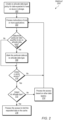
- FIG. 2 one embodiment of a method 200 for processing applications with data not expected to be reused is shown.
- the steps in this embodiment are shown in sequential order. However, in other embodiments some steps occur in a different order than shown, some steps are performed concurrently, some steps are combined with other steps, and some steps are absent.
- one particular type of calculation includes vertex shading in a graphics processing pipeline. Some vertex shading results are reused during processing, while other vertex shading results are used only a single time.
- a vertex index stored in a particular table is used to identify data that is not expected to be reused.
- program instructions are executed and storage, such as a cache, is accessed. If particular data qualifies as data that is not expected to be reused during the processing of the applications ("yes" branch of the conditional block 206), then the particular data is marked as the no allocate data type (block 208).
- the cache access is processed in a manner that limits the life of the data in the cache (block 216) as described in association with FIGs. 3 and 4 .
- the cache controller may prevent allocation of the associated data in the cache after a miss in the cache. Limiting the number of cache blocks with the no allocate data type by performing these steps leaves more room in the cache for data more likely to be reused.
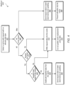
- FIG. 3 one embodiment of a method 300 for performing a read access request for data not expected to be reused is shown.
- a data access request is detected (block 302) and a cache is accessed for the data.
- multiple methods may be used to determine whether data corresponding to an access request is of the no allocate data type.
- the read request is for data of the no allocate data type.
- a lookup operation into the cache is performed for the read request. If a hit occurs ("yes" branch of the conditional block 304), then the requested data is read from the cache array and returned to the requestor (block 306).
- the cache controller does not update the accessed cache block to indicate this most recent access (block 308). For example, the cache controller does not update data used for a cache replacement policy based on the access. In one embodiment, an age of last use of the data or any other least recently used (LRU) information is not updated. Therefore, the access does not increase the amount of time that the data remains in the cache. Rather, the cache replacement policy data for the accessed cache data remains unchanged as though the access had not occurred.
- LRU least recently used
- a cache is accessed for data.
- multiple methods are used to determine whether data corresponding to an access request is of the no allocate data type.
- a cache write request for data of the no allocate data type is detected (block 402). 402).
- a lookup operation into the cache is performed for the write request. If a hit occurs ("yes" branch of the conditional block 404), and no indication for bypassing the cache is detected ("no" branch of the conditional block 410), then the write request data is written into the cache array (block 412).
- the cache controller does not update the cache replacement policy data, such as least recently used data, for the cache block (block 414). Therefore, the life of the data in the cache is not extended due to the access.
- reducing the amount of data of the no allocate data type in the cache becomes more aggressive. For example, if the data stored in the cache and being targeted by the write request is clean (unmodified) ("yes" branch of the conditional block 416), then the targeted data is deallocated (or invalidated) from the cache (block 418) and the write request data is sent to lower-level memory for updating the copy of the targeted data in the lower-level memory (block 420).
- control flow of method 400 moves to block 412 where the write request data is written into the cache array.
- both clean and dirty sub-blocks are identified within the targeted data.
- the sub-blocks are one or more bytes within a multi-byte cache line. A bit vector is used to indicate which sub-blocks are clean and which sub-blocks are dirty.
- the clean sub-blocks are deallocated from the cache while the dirty sub-blocks remain. If any of the dirty sub-blocks are targeted by the write request, then they are modified within the cache with the write request data. If any of the clean sub-blocks are targeted by the write request, then they are modified in the lower-level memory with the write request data.
- the write request data is sent to lower-level memory for updating the targeted data (block 406).
- the targeted data is prevented from being allocated into the cache (block 408). Therefore, the amount of data of the limited reuse data type is reduced in the cache.
- a computer accessible storage medium includes any storage media accessible by a computer during use to provide instructions and/or data to the computer.
- a computer accessible storage medium includes storage media such as magnetic or optical media, e.g., disk (fixed or removable), tape, CD-ROM, or DVD-ROM, CD-R, CD-RW, DVD-R, DVD-RW, or Blu-Ray.
- Storage media further includes volatile or non-volatile memory media such as RAM (e.g. synchronous dynamic RAM (SDRAM), double data rate (DDR, DDR2, DDR3, etc.) SDRAM, low-power DDR (LPDDR2, etc.) SDRAM, Rambus DRAM (RDRAM), static RAM (SRAM), etc.), ROM, Flash memory, non-volatile memory (e.g. Flash memory) accessible via a peripheral interface such as the Universal Serial Bus (USB) interface, etc.
- SDRAM synchronous dynamic RAM
- DDR double data rate SDRAM
- LPDDR2, etc. low-power DDR
- RDRAM Rambus DRAM
- SRAM static RAM
- ROM Flash memory
- non-volatile memory e.g. Flash memory
- USB
- program instructions include behavioral-level descriptions or register-transfer level (RTL) descriptions of the hardware functionality in a high level programming language such as C, or a design language (HDL) such as Verilog, VHDL, or database format such as GDS II stream format (GDSII).
- RTL register-transfer level
- HDL design language
- GDSII database format
- the description is read by a synthesis tool, which synthesizes the description to produce a netlist including a list of gates from a synthesis library.
- the netlist includes a set of gates, which also represent the functionality of the hardware including the system.
- the netlist is then placed and routed to produce a data set describing geometric shapes to be applied to masks.
- the masks are then used in various semiconductor fabrication steps to produce a semiconductor circuit or circuits corresponding to the system.
- the instructions on the computer accessible storage medium are the netlist (with or without the synthesis library) or the data set, as desired. Additionally, the instructions are utilized for purposes of emulation by a hardware based type emulator from such vendors as Cadence ® , EVE ® , and Mentor Graphics ® .
Landscapes
- Engineering & Computer Science (AREA)
- Theoretical Computer Science (AREA)
- Physics & Mathematics (AREA)
- General Engineering & Computer Science (AREA)
- General Physics & Mathematics (AREA)
- Memory System Of A Hierarchy Structure (AREA)
Claims (15)
- Rechensystem, umfassend:einen Cache, umfassend eine Vielzahl von Blöcken zum Speichern von Daten; undeine Cache-Steuerung, die mit dem Cache gekoppelt ist, wobei die Cache-Steuerung als Reaktion auf das Erkennen einer Zugriffsanforderung für bestimmte Daten konfiguriert ist zum:Bestimmen, ob für die vorgegebenen Daten eine Wiederverwendung erwartet wird; undals Reaktion auf das Bestimmen, dass die Zugriffsanforderung in dem Cache fehlt:Zuordnen der vorgegebenen Daten im Cache und Speichern einer Zählung, die angibt, wie oft die vorgegebenen Daten voraussichtlich verwendet werden, als Reaktion auf das Bestimmen, dass für die vorgegebenen Daten eine Wiederverwendung erwartet wird; undVerhindern des Zuordnens der vorgegebenen Daten im Cache, als Reaktion darauf, dass bestimmt wird, dass für die vorgegebenen Daten voraussichtlich keine Wiederverwendung erwartet wird.
- Computersystem nach Anspruch 1, wobei die Cache-Steuerung als Reaktion auf das Bestimmen der Zugriffsanforderungstreffer im Cache die Cache-Ersetzungsrichtlinieninformationen für die vorgegebenen Daten im Cache als Reaktion auf den Zugriff nicht aktualisiert.
- Computersystem nach Anspruch 2, wobei es sich bei den Cache-Ersetzungsrichtlinieninformationen um zuletzt verwendete Daten handelt.
- Computersystem nach Anspruch 1, wobei das Bestimmen, ob für die vorgegebenen Daten eine Wiederverwendung erwartet wird, das Erkennen einer Angabe in der Zugriffsanforderung umfasst, die angibt, ob für die vorgegebenen Daten eine Wiederverwendung erwartet wird.
- Computersystem nach Anspruch 1, wobei das Bestimmen, ob für die vorgegebenen Daten eine Wiederverwendung erwartet wird, das Bestimmen umfasst, dass die Zugriffsanforderung eine Adresse innerhalb eines vorgegebenen Adressbereichs angibt.
- Computersystem nach Anspruch 1, wobei das Bestimmen, dass die vorgegebenen Daten voraussichtlich nicht wiederverwendet werden, das Bestimmen umfasst, dass die vorgegebenen Daten Ergebnisse einer Vertex-Schattierung in einer Grafik-Pipeline umfassen.
- Computersystem nach Anspruch 1, wobei die Cache-Steuerung ferner so konfiguriert ist, dass er die Zuordnung der vorgegebenen Daten aus dem Cache ohne Änderung durch Schreiben von Daten aufhebt, und zwar in Reaktion auf:Bestimmen, dass es sich bei der Zugriffsanforderung um eine Schreibanforderung handelt, die im Cache auftaucht; undErkennen, dass die vorgegebenen Daten im Cache sauber sind.
- Computersystem nach Anspruch 1, wobei die Cache-Steuerung ferner so konfiguriert ist, dass er die Zählung bei jedem Zugriff auf die vorgegebenen Daten aktualisiert.
- Computersystem nach Anspruch 7, wobei die Cache-Steuerung ferner konfiguriert ist zum:Identifizieren von sowohl sauberen als auch schmutzigen Unterblöcke innerhalb der vorgegebenen Daten;Aufheben der Zuordnung der sauberen Unterblöcke aus dem Cache ohne Änderung zu Schreibanforderungsdaten; undÄndern der schmutzigen Unterblöcke mit Schreibanforderungsdaten.
- Verfahren zum Verwalten von Daten in einem Speichersystem, wobei das Verfahren umfasst:Schnittstellenlogik, die eine Anforderung für den Zugriff auf vorgegebene, im Speichersystem gespeicherte Daten empfängt;Cache-Steuerungslogik:Bestimmen, ob für die vorgegebenen Daten eine Wiederverwendung erwartet wird;als Reaktion auf das Bestimmen, dass die Zugriffsanforderung in dem Cache fehlt:Zuordnen der vorgegebenen Daten im Cache und Speichern einer Zählung, die angibt, wie oft die vorgegebenen Daten voraussichtlich verwendet werden, als Reaktion auf das Bestimmen, dass für die vorgegebenen Daten eine Wiederverwendung erwartet wird; undVerhindern des Zuordnens der vorgegebenen Daten im Cache als Reaktion auf das Bestimmen, dass für die vorgegebenen Daten keine Wiederverwendung erwartet wird.
- Verfahren nach Anspruch 10, wobei das Verfahren als Reaktion auf das Bestimmen der Zugriffsanforderungstreffer im Cache ferner das Verhindern einer Aktualisierung von Cache-Ersetzungsrichtlinieninformationen für die vorgegebenen Daten als Reaktion auf den Zugriff umfasst.
- Verfahren nach Anspruch 11, wobei es sich bei den Cache-Ersetzungsrichtlinieninformationen um zuletzt verwendete Daten handelt.
- Verfahren nach Anspruch 10, ferner umfassend das Aufheben der Zuordnung der vorgegebenen Daten aus dem Cache ohne Ändern durch die Schreibanforderung als Reaktion auf:Bestimmen, dass es sich bei der Zugriffsanforderung um eine Schreibanforderung handelt, die im Cache auftaucht; undErkennen, dass die vorgegebenen Daten im Cache sauber sind.
- Verfahren nach Anspruch 10, wobei das Bestimmen, dass die vorgegebenen Daten voraussichtlich nicht wiederverwendet werden, das Bestimmen umfasst, dass die vorgegebenen Daten Ergebnisse einer Vertex-Schattierung in einer Grafik-Pipeline umfassen.
- Cache-Steuerung, umfassend:eine erste Schnittstelle, die mit einem Cache gekoppelt ist, der eine Vielzahl von Blöcken zum Speichern von Daten umfasst; undeine Steuereinheit; undwobei die Steuereinheit als Reaktion auf das Erkennen einer Zugriffsanforderung für vorgegebene Daten konfiguriert ist zum:Bestimmen, ob für die vorgegebenen Daten eine Wiederverwendung erwartet wird;als Reaktion auf das Bestimmen, dass die Zugriffsanforderung in dem Cache fehlt:Zuordnen der vorgegebenen Daten im Cache und Speichern einer Zählung, die angibt, wie oft die vorgegebenen Daten voraussichtlich verwendet werden, als Reaktion auf das Bestimmen, dass für die vorgegebenen Daten eine Wiederverwendung erwartet wird; undVerhindern des Zuordnens der vorgegebenen Daten im Cache, als Reaktion darauf, dass bestimmt wird, dass für die vorgegebenen Daten voraussichtlich keine Wiederverwendung erwartet wird.
Applications Claiming Priority (2)
| Application Number | Priority Date | Filing Date | Title |
|---|---|---|---|
| US15/374,788 US9996478B1 (en) | 2016-12-09 | 2016-12-09 | No allocate cache policy |
| PCT/US2017/065094 WO2018106906A1 (en) | 2016-12-09 | 2017-12-07 | No allocate cache policy |
Publications (2)
| Publication Number | Publication Date |
|---|---|
| EP3552110A1 EP3552110A1 (de) | 2019-10-16 |
| EP3552110B1 true EP3552110B1 (de) | 2025-01-29 |
Family
ID=60888634
Family Applications (1)
| Application Number | Title | Priority Date | Filing Date |
|---|---|---|---|
| EP17822865.6A Active EP3552110B1 (de) | 2016-12-09 | 2017-12-07 | Cache-richtlinie zur verhinderung von zuweisung |
Country Status (6)
| Country | Link |
|---|---|
| US (1) | US9996478B1 (de) |
| EP (1) | EP3552110B1 (de) |
| JP (1) | JP7072573B2 (de) |
| KR (1) | KR102540752B1 (de) |
| CN (1) | CN110036376B (de) |
| WO (1) | WO2018106906A1 (de) |
Families Citing this family (7)
| Publication number | Priority date | Publication date | Assignee | Title |
|---|---|---|---|---|
| CN108984104B (zh) | 2017-06-02 | 2021-09-17 | 伊姆西Ip控股有限责任公司 | 用于缓存管理的方法和设备 |
| US10922237B2 (en) * | 2018-09-12 | 2021-02-16 | Advanced Micro Devices, Inc. | Accelerating accesses to private regions in a region-based cache directory scheme |
| CN112559389B (zh) * | 2019-09-25 | 2025-02-25 | 阿里巴巴集团控股有限公司 | 存储控制装置、处理装置、计算机系统和存储控制方法 |
| US11768779B2 (en) * | 2019-12-16 | 2023-09-26 | Advanced Micro Devices, Inc. | Cache management based on access type priority |
| CN111813712B (zh) * | 2019-12-31 | 2025-08-29 | 泰斗微电子科技有限公司 | 一种缓存分配控制方法、装置、终端设备及存储介质 |
| US11403034B1 (en) * | 2021-06-11 | 2022-08-02 | International Business Machines Corporation | Non-volatile storage class memory data flow with mismatched block sizes |
| US12117939B2 (en) * | 2021-12-21 | 2024-10-15 | Advanced Micro Devices, Inc. | Stochastic optimization of surface cacheability in parallel processing units |
Family Cites Families (14)
| Publication number | Priority date | Publication date | Assignee | Title |
|---|---|---|---|---|
| JPH01133162A (ja) * | 1987-11-18 | 1989-05-25 | Fujitsu Ltd | キャッシュメモリ制御方式 |
| US6275904B1 (en) | 1998-03-31 | 2001-08-14 | Intel Corporation | Cache pollution avoidance instructions |
| US6574708B2 (en) * | 2001-05-18 | 2003-06-03 | Broadcom Corporation | Source controlled cache allocation |
| US7356650B1 (en) * | 2005-06-17 | 2008-04-08 | Unisys Corporation | Cache apparatus and method for accesses lacking locality |
| US7415575B1 (en) * | 2005-12-08 | 2008-08-19 | Nvidia, Corporation | Shared cache with client-specific replacement policy |
| US8230179B2 (en) | 2008-05-15 | 2012-07-24 | International Business Machines Corporation | Administering non-cacheable memory load instructions |
| US8589629B2 (en) * | 2009-03-27 | 2013-11-19 | Advanced Micro Devices, Inc. | Method for way allocation and way locking in a cache |
| US8392658B2 (en) * | 2009-07-10 | 2013-03-05 | Apple Inc. | Cache implementing multiple replacement policies |
| US8542247B1 (en) * | 2009-07-17 | 2013-09-24 | Nvidia Corporation | Cull before vertex attribute fetch and vertex lighting |
| US9158685B2 (en) * | 2012-09-11 | 2015-10-13 | Apple Inc. | System cache with cache hint control |
| US20140089600A1 (en) * | 2012-09-27 | 2014-03-27 | Apple Inc. | System cache with data pending state |
| KR102100161B1 (ko) | 2014-02-04 | 2020-04-14 | 삼성전자주식회사 | Gpu 데이터 캐싱 방법 및 그에 따른 데이터 프로세싱 시스템 |
| US9720837B2 (en) | 2014-06-27 | 2017-08-01 | International Business Machines Corporation | Allowing non-cacheable loads within a transaction |
| US20160041914A1 (en) * | 2014-08-05 | 2016-02-11 | Advanced Micro Devices, Inc. | Cache Bypassing Policy Based on Prefetch Streams |
-
2016
- 2016-12-09 US US15/374,788 patent/US9996478B1/en active Active
-
2017
- 2017-12-07 JP JP2019530390A patent/JP7072573B2/ja active Active
- 2017-12-07 EP EP17822865.6A patent/EP3552110B1/de active Active
- 2017-12-07 KR KR1020197017353A patent/KR102540752B1/ko active Active
- 2017-12-07 CN CN201780075187.3A patent/CN110036376B/zh active Active
- 2017-12-07 WO PCT/US2017/065094 patent/WO2018106906A1/en not_active Ceased
Also Published As
| Publication number | Publication date |
|---|---|
| JP2019537162A (ja) | 2019-12-19 |
| JP7072573B2 (ja) | 2022-05-20 |
| KR20190092444A (ko) | 2019-08-07 |
| WO2018106906A1 (en) | 2018-06-14 |
| KR102540752B1 (ko) | 2023-06-08 |
| US9996478B1 (en) | 2018-06-12 |
| CN110036376A (zh) | 2019-07-19 |
| EP3552110A1 (de) | 2019-10-16 |
| US20180165221A1 (en) | 2018-06-14 |
| CN110036376B (zh) | 2023-07-07 |
Similar Documents
| Publication | Publication Date | Title |
|---|---|---|
| EP3552110B1 (de) | Cache-richtlinie zur verhinderung von zuweisung | |
| US9075730B2 (en) | Mechanisms to bound the presence of cache blocks with specific properties in caches | |
| US9552294B2 (en) | Dynamically configuring regions of a main memory in a write-back mode or a write-through mode | |
| US10725923B1 (en) | Cache access detection and prediction | |
| US10019369B2 (en) | Apparatuses and methods for pre-fetching and write-back for a segmented cache memory | |
| US9251081B2 (en) | Management of caches | |
| US9223710B2 (en) | Read-write partitioning of cache memory | |
| US8606997B2 (en) | Cache hierarchy with bounds on levels accessed | |
| US9251069B2 (en) | Mechanisms to bound the presence of cache blocks with specific properties in caches | |
| US9378153B2 (en) | Early write-back of modified data in a cache memory | |
| US20140181402A1 (en) | Selective cache memory write-back and replacement policies | |
| US9317448B2 (en) | Methods and apparatus related to data processors and caches incorporated in data processors | |
| US9892039B2 (en) | Non-temporal write combining using cache resources | |
| US10545887B2 (en) | Multiple linked list data structure | |
| US20170083444A1 (en) | Configuring fast memory as cache for slow memory | |
| US20180095884A1 (en) | Mass storage cache in non volatile level of multi-level system memory | |
| CN111480151B (zh) | 将高速缓存线从共用存储器页面冲洗到存储器 | |
| US20170357596A1 (en) | Dynamically adjustable inclusion bias for inclusive caches | |
| US11526449B2 (en) | Limited propagation of unnecessary memory updates | |
| US9128856B2 (en) | Selective cache fills in response to write misses | |
| US7472225B2 (en) | Caching data | |
| EP3258383A1 (de) | Dynamisch verstellbare inklusionsvorspannung für inklusive cachespeicher | |
| US20200133884A1 (en) | Nvram system memory with memory side cache that favors written to items and/or includes regions with customized temperature induced speed settings | |
| CN115729860A (zh) | 处理系统、处理方法及电子设备 | |
| JP2019164497A (ja) | 管理装置、情報処理装置、管理方法、およびプログラム |
Legal Events
| Date | Code | Title | Description |
|---|---|---|---|
| STAA | Information on the status of an ep patent application or granted ep patent |
Free format text: STATUS: UNKNOWN |
|
| STAA | Information on the status of an ep patent application or granted ep patent |
Free format text: STATUS: THE INTERNATIONAL PUBLICATION HAS BEEN MADE |
|
| PUAI | Public reference made under article 153(3) epc to a published international application that has entered the european phase |
Free format text: ORIGINAL CODE: 0009012 |
|
| STAA | Information on the status of an ep patent application or granted ep patent |
Free format text: STATUS: REQUEST FOR EXAMINATION WAS MADE |
|
| 17P | Request for examination filed |
Effective date: 20190528 |
|
| AK | Designated contracting states |
Kind code of ref document: A1 Designated state(s): AL AT BE BG CH CY CZ DE DK EE ES FI FR GB GR HR HU IE IS IT LI LT LU LV MC MK MT NL NO PL PT RO RS SE SI SK SM TR |
|
| AX | Request for extension of the european patent |
Extension state: BA ME |
|
| DAV | Request for validation of the european patent (deleted) | ||
| DAX | Request for extension of the european patent (deleted) | ||
| STAA | Information on the status of an ep patent application or granted ep patent |
Free format text: STATUS: EXAMINATION IS IN PROGRESS |
|
| 17Q | First examination report despatched |
Effective date: 20211029 |
|
| GRAP | Despatch of communication of intention to grant a patent |
Free format text: ORIGINAL CODE: EPIDOSNIGR1 |
|
| STAA | Information on the status of an ep patent application or granted ep patent |
Free format text: STATUS: GRANT OF PATENT IS INTENDED |
|
| INTG | Intention to grant announced |
Effective date: 20240816 |
|
| GRAS | Grant fee paid |
Free format text: ORIGINAL CODE: EPIDOSNIGR3 |
|
| P01 | Opt-out of the competence of the unified patent court (upc) registered |
Free format text: CASE NUMBER: APP_61790/2024 Effective date: 20241119 |
|
| GRAA | (expected) grant |
Free format text: ORIGINAL CODE: 0009210 |
|
| STAA | Information on the status of an ep patent application or granted ep patent |
Free format text: STATUS: THE PATENT HAS BEEN GRANTED |
|
| AK | Designated contracting states |
Kind code of ref document: B1 Designated state(s): AL AT BE BG CH CY CZ DE DK EE ES FI FR GB GR HR HU IE IS IT LI LT LU LV MC MK MT NL NO PL PT RO RS SE SI SK SM TR |
|
| REG | Reference to a national code |
Ref country code: GB Ref legal event code: FG4D |
|
| REG | Reference to a national code |
Ref country code: CH Ref legal event code: EP |
|
| REG | Reference to a national code |
Ref country code: DE Ref legal event code: R096 Ref document number: 602017087572 Country of ref document: DE |
|
| REG | Reference to a national code |
Ref country code: IE Ref legal event code: FG4D |
|
| REG | Reference to a national code |
Ref country code: NL Ref legal event code: MP Effective date: 20250129 |
|
| PG25 | Lapsed in a contracting state [announced via postgrant information from national office to epo] |
Ref country code: NL Free format text: LAPSE BECAUSE OF FAILURE TO SUBMIT A TRANSLATION OF THE DESCRIPTION OR TO PAY THE FEE WITHIN THE PRESCRIBED TIME-LIMIT Effective date: 20250129 |
|
| PG25 | Lapsed in a contracting state [announced via postgrant information from national office to epo] |
Ref country code: RS Free format text: LAPSE BECAUSE OF FAILURE TO SUBMIT A TRANSLATION OF THE DESCRIPTION OR TO PAY THE FEE WITHIN THE PRESCRIBED TIME-LIMIT Effective date: 20250429 |
|
| PG25 | Lapsed in a contracting state [announced via postgrant information from national office to epo] |
Ref country code: FI Free format text: LAPSE BECAUSE OF FAILURE TO SUBMIT A TRANSLATION OF THE DESCRIPTION OR TO PAY THE FEE WITHIN THE PRESCRIBED TIME-LIMIT Effective date: 20250129 |
|
| PG25 | Lapsed in a contracting state [announced via postgrant information from national office to epo] |
Ref country code: PL Free format text: LAPSE BECAUSE OF FAILURE TO SUBMIT A TRANSLATION OF THE DESCRIPTION OR TO PAY THE FEE WITHIN THE PRESCRIBED TIME-LIMIT Effective date: 20250129 |
|
| PG25 | Lapsed in a contracting state [announced via postgrant information from national office to epo] |
Ref country code: ES Free format text: LAPSE BECAUSE OF FAILURE TO SUBMIT A TRANSLATION OF THE DESCRIPTION OR TO PAY THE FEE WITHIN THE PRESCRIBED TIME-LIMIT Effective date: 20250129 |
|
| REG | Reference to a national code |
Ref country code: LT Ref legal event code: MG9D |
|
| PG25 | Lapsed in a contracting state [announced via postgrant information from national office to epo] |
Ref country code: NO Free format text: LAPSE BECAUSE OF FAILURE TO SUBMIT A TRANSLATION OF THE DESCRIPTION OR TO PAY THE FEE WITHIN THE PRESCRIBED TIME-LIMIT Effective date: 20250429 Ref country code: IS Free format text: LAPSE BECAUSE OF FAILURE TO SUBMIT A TRANSLATION OF THE DESCRIPTION OR TO PAY THE FEE WITHIN THE PRESCRIBED TIME-LIMIT Effective date: 20250529 |
|
| REG | Reference to a national code |
Ref country code: AT Ref legal event code: MK05 Ref document number: 1764132 Country of ref document: AT Kind code of ref document: T Effective date: 20250129 |
|
| PG25 | Lapsed in a contracting state [announced via postgrant information from national office to epo] |
Ref country code: HR Free format text: LAPSE BECAUSE OF FAILURE TO SUBMIT A TRANSLATION OF THE DESCRIPTION OR TO PAY THE FEE WITHIN THE PRESCRIBED TIME-LIMIT Effective date: 20250129 |
|
| PG25 | Lapsed in a contracting state [announced via postgrant information from national office to epo] |
Ref country code: LV Free format text: LAPSE BECAUSE OF FAILURE TO SUBMIT A TRANSLATION OF THE DESCRIPTION OR TO PAY THE FEE WITHIN THE PRESCRIBED TIME-LIMIT Effective date: 20250129 Ref country code: PT Free format text: LAPSE BECAUSE OF FAILURE TO SUBMIT A TRANSLATION OF THE DESCRIPTION OR TO PAY THE FEE WITHIN THE PRESCRIBED TIME-LIMIT Effective date: 20250529 |
|
| PG25 | Lapsed in a contracting state [announced via postgrant information from national office to epo] |
Ref country code: BG Free format text: LAPSE BECAUSE OF FAILURE TO SUBMIT A TRANSLATION OF THE DESCRIPTION OR TO PAY THE FEE WITHIN THE PRESCRIBED TIME-LIMIT Effective date: 20250129 Ref country code: GR Free format text: LAPSE BECAUSE OF FAILURE TO SUBMIT A TRANSLATION OF THE DESCRIPTION OR TO PAY THE FEE WITHIN THE PRESCRIBED TIME-LIMIT Effective date: 20250430 |
|
| PG25 | Lapsed in a contracting state [announced via postgrant information from national office to epo] |
Ref country code: AT Free format text: LAPSE BECAUSE OF FAILURE TO SUBMIT A TRANSLATION OF THE DESCRIPTION OR TO PAY THE FEE WITHIN THE PRESCRIBED TIME-LIMIT Effective date: 20250129 |
|
| PG25 | Lapsed in a contracting state [announced via postgrant information from national office to epo] |
Ref country code: SE Free format text: LAPSE BECAUSE OF FAILURE TO SUBMIT A TRANSLATION OF THE DESCRIPTION OR TO PAY THE FEE WITHIN THE PRESCRIBED TIME-LIMIT Effective date: 20250129 |
|
| PG25 | Lapsed in a contracting state [announced via postgrant information from national office to epo] |
Ref country code: SM Free format text: LAPSE BECAUSE OF FAILURE TO SUBMIT A TRANSLATION OF THE DESCRIPTION OR TO PAY THE FEE WITHIN THE PRESCRIBED TIME-LIMIT Effective date: 20250129 |
|
| PG25 | Lapsed in a contracting state [announced via postgrant information from national office to epo] |
Ref country code: DK Free format text: LAPSE BECAUSE OF FAILURE TO SUBMIT A TRANSLATION OF THE DESCRIPTION OR TO PAY THE FEE WITHIN THE PRESCRIBED TIME-LIMIT Effective date: 20250129 |
|
| PG25 | Lapsed in a contracting state [announced via postgrant information from national office to epo] |
Ref country code: IT Free format text: LAPSE BECAUSE OF FAILURE TO SUBMIT A TRANSLATION OF THE DESCRIPTION OR TO PAY THE FEE WITHIN THE PRESCRIBED TIME-LIMIT Effective date: 20250129 |
|
| PG25 | Lapsed in a contracting state [announced via postgrant information from national office to epo] |
Ref country code: EE Free format text: LAPSE BECAUSE OF FAILURE TO SUBMIT A TRANSLATION OF THE DESCRIPTION OR TO PAY THE FEE WITHIN THE PRESCRIBED TIME-LIMIT Effective date: 20250129 Ref country code: CZ Free format text: LAPSE BECAUSE OF FAILURE TO SUBMIT A TRANSLATION OF THE DESCRIPTION OR TO PAY THE FEE WITHIN THE PRESCRIBED TIME-LIMIT Effective date: 20250129 |
|
| PG25 | Lapsed in a contracting state [announced via postgrant information from national office to epo] |
Ref country code: RO Free format text: LAPSE BECAUSE OF FAILURE TO SUBMIT A TRANSLATION OF THE DESCRIPTION OR TO PAY THE FEE WITHIN THE PRESCRIBED TIME-LIMIT Effective date: 20250129 |
|
| PG25 | Lapsed in a contracting state [announced via postgrant information from national office to epo] |
Ref country code: SK Free format text: LAPSE BECAUSE OF FAILURE TO SUBMIT A TRANSLATION OF THE DESCRIPTION OR TO PAY THE FEE WITHIN THE PRESCRIBED TIME-LIMIT Effective date: 20250129 |
|
| REG | Reference to a national code |
Ref country code: DE Ref legal event code: R097 Ref document number: 602017087572 Country of ref document: DE |
|
| PLBE | No opposition filed within time limit |
Free format text: ORIGINAL CODE: 0009261 |
|
| STAA | Information on the status of an ep patent application or granted ep patent |
Free format text: STATUS: NO OPPOSITION FILED WITHIN TIME LIMIT |
|
| 26N | No opposition filed |
Effective date: 20251030 |
|
| PGFP | Annual fee paid to national office [announced via postgrant information from national office to epo] |
Ref country code: DE Payment date: 20251113 Year of fee payment: 9 |
|
| PGFP | Annual fee paid to national office [announced via postgrant information from national office to epo] |
Ref country code: GB Payment date: 20251203 Year of fee payment: 9 |