EP3550437B1 - Adaptive spatial access prefetcher apparatus and method - Google Patents
Adaptive spatial access prefetcher apparatus and method Download PDFInfo
- Publication number
- EP3550437B1 EP3550437B1 EP19160661.5A EP19160661A EP3550437B1 EP 3550437 B1 EP3550437 B1 EP 3550437B1 EP 19160661 A EP19160661 A EP 19160661A EP 3550437 B1 EP3550437 B1 EP 3550437B1
- Authority
- EP
- European Patent Office
- Prior art keywords
- instruction
- processor
- field
- data
- pattern
- Prior art date
- Legal status (The legal status is an assumption and is not a legal conclusion. Google has not performed a legal analysis and makes no representation as to the accuracy of the status listed.)
- Active
Links
- 238000000034 method Methods 0.000 title claims description 24
- 230000003044 adaptive effect Effects 0.000 title description 6
- 230000015654 memory Effects 0.000 claims description 141
- 239000000872 buffer Substances 0.000 claims description 26
- 230000008569 process Effects 0.000 claims description 5
- 239000013598 vector Substances 0.000 description 80
- 238000010586 diagram Methods 0.000 description 28
- 238000006073 displacement reaction Methods 0.000 description 21
- 238000003860 storage Methods 0.000 description 15
- 238000007667 floating Methods 0.000 description 14
- 239000000306 component Substances 0.000 description 13
- 238000012545 processing Methods 0.000 description 10
- 230000003416 augmentation Effects 0.000 description 8
- 230000006870 function Effects 0.000 description 8
- 230000002123 temporal effect Effects 0.000 description 8
- 239000003795 chemical substances by application Substances 0.000 description 7
- 238000004891 communication Methods 0.000 description 7
- 230000007246 mechanism Effects 0.000 description 7
- 238000013519 translation Methods 0.000 description 7
- 230000014616 translation Effects 0.000 description 7
- 230000006835 compression Effects 0.000 description 5
- 238000007906 compression Methods 0.000 description 5
- 238000013461 design Methods 0.000 description 5
- 230000004044 response Effects 0.000 description 5
- 238000006243 chemical reaction Methods 0.000 description 4
- 238000005516 engineering process Methods 0.000 description 4
- 230000000873 masking effect Effects 0.000 description 4
- 230000003068 static effect Effects 0.000 description 4
- 238000013459 approach Methods 0.000 description 3
- 238000004364 calculation method Methods 0.000 description 3
- 238000005457 optimization Methods 0.000 description 3
- 238000003491 array Methods 0.000 description 2
- 230000009286 beneficial effect Effects 0.000 description 2
- 230000008901 benefit Effects 0.000 description 2
- 230000008859 change Effects 0.000 description 2
- 238000012512 characterization method Methods 0.000 description 2
- 230000000295 complement effect Effects 0.000 description 2
- 238000004519 manufacturing process Methods 0.000 description 2
- 230000003287 optical effect Effects 0.000 description 2
- 230000009467 reduction Effects 0.000 description 2
- 230000010076 replication Effects 0.000 description 2
- 239000007787 solid Substances 0.000 description 2
- 238000009825 accumulation Methods 0.000 description 1
- 238000004590 computer program Methods 0.000 description 1
- 239000008358 core component Substances 0.000 description 1
- 230000008878 coupling Effects 0.000 description 1
- 238000010168 coupling process Methods 0.000 description 1
- 238000005859 coupling reaction Methods 0.000 description 1
- 230000001186 cumulative effect Effects 0.000 description 1
- 230000001419 dependent effect Effects 0.000 description 1
- 238000003780 insertion Methods 0.000 description 1
- 230000037431 insertion Effects 0.000 description 1
- 239000003607 modifier Substances 0.000 description 1
- 229910052754 neon Inorganic materials 0.000 description 1
- GKAOGPIIYCISHV-UHFFFAOYSA-N neon atom Chemical compound [Ne] GKAOGPIIYCISHV-UHFFFAOYSA-N 0.000 description 1
- 230000002093 peripheral effect Effects 0.000 description 1
- 230000001105 regulatory effect Effects 0.000 description 1
- 238000011160 research Methods 0.000 description 1
- 239000004065 semiconductor Substances 0.000 description 1
- 238000004088 simulation Methods 0.000 description 1
- 230000006886 spatial memory Effects 0.000 description 1
- 238000001228 spectrum Methods 0.000 description 1
- 239000000758 substrate Substances 0.000 description 1
- 230000001629 suppression Effects 0.000 description 1
- 238000012546 transfer Methods 0.000 description 1
- 230000001960 triggered effect Effects 0.000 description 1
Images


Classifications
-
- G—PHYSICS
- G06—COMPUTING; CALCULATING OR COUNTING
- G06F—ELECTRIC DIGITAL DATA PROCESSING
- G06F9/00—Arrangements for program control, e.g. control units
- G06F9/06—Arrangements for program control, e.g. control units using stored programs, i.e. using an internal store of processing equipment to receive or retain programs
- G06F9/30—Arrangements for executing machine instructions, e.g. instruction decode
- G06F9/38—Concurrent instruction execution, e.g. pipeline, look ahead
- G06F9/3802—Instruction prefetching
-
- G—PHYSICS
- G06—COMPUTING; CALCULATING OR COUNTING
- G06F—ELECTRIC DIGITAL DATA PROCESSING
- G06F12/00—Accessing, addressing or allocating within memory systems or architectures
- G06F12/02—Addressing or allocation; Relocation
- G06F12/08—Addressing or allocation; Relocation in hierarchically structured memory systems, e.g. virtual memory systems
- G06F12/0802—Addressing of a memory level in which the access to the desired data or data block requires associative addressing means, e.g. caches
- G06F12/0806—Multiuser, multiprocessor or multiprocessing cache systems
- G06F12/0811—Multiuser, multiprocessor or multiprocessing cache systems with multilevel cache hierarchies
-
- G—PHYSICS
- G06—COMPUTING; CALCULATING OR COUNTING
- G06F—ELECTRIC DIGITAL DATA PROCESSING
- G06F12/00—Accessing, addressing or allocating within memory systems or architectures
- G06F12/02—Addressing or allocation; Relocation
- G06F12/08—Addressing or allocation; Relocation in hierarchically structured memory systems, e.g. virtual memory systems
- G06F12/0802—Addressing of a memory level in which the access to the desired data or data block requires associative addressing means, e.g. caches
- G06F12/0806—Multiuser, multiprocessor or multiprocessing cache systems
- G06F12/084—Multiuser, multiprocessor or multiprocessing cache systems with a shared cache
-
- G—PHYSICS
- G06—COMPUTING; CALCULATING OR COUNTING
- G06F—ELECTRIC DIGITAL DATA PROCESSING
- G06F12/00—Accessing, addressing or allocating within memory systems or architectures
- G06F12/02—Addressing or allocation; Relocation
- G06F12/08—Addressing or allocation; Relocation in hierarchically structured memory systems, e.g. virtual memory systems
- G06F12/0802—Addressing of a memory level in which the access to the desired data or data block requires associative addressing means, e.g. caches
- G06F12/0806—Multiuser, multiprocessor or multiprocessing cache systems
- G06F12/0842—Multiuser, multiprocessor or multiprocessing cache systems for multiprocessing or multitasking
-
- G—PHYSICS
- G06—COMPUTING; CALCULATING OR COUNTING
- G06F—ELECTRIC DIGITAL DATA PROCESSING
- G06F12/00—Accessing, addressing or allocating within memory systems or architectures
- G06F12/02—Addressing or allocation; Relocation
- G06F12/08—Addressing or allocation; Relocation in hierarchically structured memory systems, e.g. virtual memory systems
- G06F12/0802—Addressing of a memory level in which the access to the desired data or data block requires associative addressing means, e.g. caches
- G06F12/0862—Addressing of a memory level in which the access to the desired data or data block requires associative addressing means, e.g. caches with prefetch
-
- G—PHYSICS
- G06—COMPUTING; CALCULATING OR COUNTING
- G06F—ELECTRIC DIGITAL DATA PROCESSING
- G06F12/00—Accessing, addressing or allocating within memory systems or architectures
- G06F12/02—Addressing or allocation; Relocation
- G06F12/08—Addressing or allocation; Relocation in hierarchically structured memory systems, e.g. virtual memory systems
- G06F12/0802—Addressing of a memory level in which the access to the desired data or data block requires associative addressing means, e.g. caches
- G06F12/0875—Addressing of a memory level in which the access to the desired data or data block requires associative addressing means, e.g. caches with dedicated cache, e.g. instruction or stack
-
- G—PHYSICS
- G06—COMPUTING; CALCULATING OR COUNTING
- G06F—ELECTRIC DIGITAL DATA PROCESSING
- G06F9/00—Arrangements for program control, e.g. control units
- G06F9/06—Arrangements for program control, e.g. control units using stored programs, i.e. using an internal store of processing equipment to receive or retain programs
- G06F9/30—Arrangements for executing machine instructions, e.g. instruction decode
- G06F9/38—Concurrent instruction execution, e.g. pipeline, look ahead
- G06F9/3802—Instruction prefetching
- G06F9/3804—Instruction prefetching for branches, e.g. hedging, branch folding
- G06F9/3806—Instruction prefetching for branches, e.g. hedging, branch folding using address prediction, e.g. return stack, branch history buffer
-
- G—PHYSICS
- G06—COMPUTING; CALCULATING OR COUNTING
- G06F—ELECTRIC DIGITAL DATA PROCESSING
- G06F9/00—Arrangements for program control, e.g. control units
- G06F9/06—Arrangements for program control, e.g. control units using stored programs, i.e. using an internal store of processing equipment to receive or retain programs
- G06F9/30—Arrangements for executing machine instructions, e.g. instruction decode
- G06F9/38—Concurrent instruction execution, e.g. pipeline, look ahead
- G06F9/3836—Instruction issuing, e.g. dynamic instruction scheduling or out of order instruction execution
- G06F9/3842—Speculative instruction execution
-
- G—PHYSICS
- G06—COMPUTING; CALCULATING OR COUNTING
- G06F—ELECTRIC DIGITAL DATA PROCESSING
- G06F2212/00—Indexing scheme relating to accessing, addressing or allocation within memory systems or architectures
- G06F2212/10—Providing a specific technical effect
- G06F2212/1016—Performance improvement
- G06F2212/1021—Hit rate improvement
-
- G—PHYSICS
- G06—COMPUTING; CALCULATING OR COUNTING
- G06F—ELECTRIC DIGITAL DATA PROCESSING
- G06F2212/00—Indexing scheme relating to accessing, addressing or allocation within memory systems or architectures
- G06F2212/45—Caching of specific data in cache memory
- G06F2212/452—Instruction code
-
- G—PHYSICS
- G06—COMPUTING; CALCULATING OR COUNTING
- G06F—ELECTRIC DIGITAL DATA PROCESSING
- G06F2212/00—Indexing scheme relating to accessing, addressing or allocation within memory systems or architectures
- G06F2212/60—Details of cache memory
- G06F2212/6022—Using a prefetch buffer or dedicated prefetch cache
-
- G—PHYSICS
- G06—COMPUTING; CALCULATING OR COUNTING
- G06F—ELECTRIC DIGITAL DATA PROCESSING
- G06F2212/00—Indexing scheme relating to accessing, addressing or allocation within memory systems or architectures
- G06F2212/60—Details of cache memory
- G06F2212/6024—History based prefetching
Definitions
- the embodiments of the invention relate generally to the field of computer processors. More particularly, the embodiments relate to an adaptive spatial access prefetcher apparatus and method.
- An instruction set, or instruction set architecture is the part of the computer architecture related to programming, including the native data types, instructions, register architecture, addressing modes, memory architecture, interrupt and exception handling, and external input and output (I/O).
- instruction generally refers herein to macro-instructions - that is instructions that are provided to the processor for execution - as opposed to micro-instructions or micro-ops - that is the result of a processor's decoder decoding macro-instructions.
- the micro-instructions or micro-ops can be configured to instruct an execution unit on the processor to perform operations to implement the logic associated with the macro-instruction.
- the ISA is distinguished from the microarchitecture, which is the set of processor design techniques used to implement the instruction set.
- Processors with different microarchitectures can share a common instruction set. For example, Intel® Pentium 4 processors, Intel® CoreTM processors, and processors from Advanced Micro Devices, Inc. of Sunnyvale CA implement nearly identical versions of the x86 instruction set (with some extensions that have been added with newer versions), but have different internal designs.
- the same register architecture of the ISA may be implemented in different ways in different microarchitectures using well-known techniques, including dedicated physical registers, one or more dynamically allocated physical registers using a register renaming mechanism (e.g., the use of a Register Alias Table (RAT), a Reorder Buffer (ROB) and a retirement register file).
- a register renaming mechanism e.g., the use of a Register Alias Table (RAT), a Reorder Buffer (ROB) and a retirement register file.
- RAT Register Alias Table
- ROB Reorder Buffer
- retirement register file e.g., the phrases register architecture, register file, and register are used herein to refer to that which is visible to the software/programmer and the manner in which instructions specify registers.
- the adjective "logical,” “architectural,” or “software visible” will be used to indicate registers/files in the register architecture, while different adjectives will be used to designate registers in a given microarchitecture (e.g., physical register, reorder buffer, retirement register, register pool).
- US 2018/089087 A1 relates to an improved flash-based memory module, and a method of operating the same.
- a method of storing data in a memory module including an in-module prefetcher, an in-module prefetch buffer, memory, and a memory controller, the method including sending address information from the in-module prefetcher to the memory controller and to the prefetch buffer, determining prefetch accuracy based on a comparison of the address information sent to the memory controller and the address information sent to the prefetch buffer, determining a prefetch mode based on the prefetch accuracy, and storing the data in the memory based on the prefetch mode.
- EP 3 285 172 A1 relates to a data cache region prefetcher creating a region when a data cache miss occurs.
- Each region includes a predetermined range of data lines proximate to each data cache miss and is tagged with an associated instruction pointer register (RIP).
- the data cache region prefetcher compares subsequent memory requests against the predetermined range of data lines for each of the existing regions. For each match, the data cache region prefetcher sets an access bit and attempts to identify a pseudo-random access pattern based on the set access bits.
- the data cache region prefetcher increments or decrements appropriate counters to track how often the pseudo-random access pattern occurs. If the pseudo-random access pattern occurs frequently, then the next time a memory request is processed with the same RIP and pattern, the data cache region prefetcher prefetches the data lines in accordance with the pseudo-random access pattern for that RIP.
- An instruction set includes one or more instruction formats.
- a given instruction format defines various fields (number of bits, location of bits) to specify, among other things, the operation to be performed (opcode) and the operand(s) on which that operation is to be performed.
- Some instruction formats are further broken down though the definition of instruction templates (or subformats).
- the instruction templates of a given instruction format may be defined to have different subsets of the instruction format's fields (the included fields are typically in the same order, but at least some have different bit positions because there are less fields included) and/or defined to have a given field interpreted differently.
- each instruction of an ISA is expressed using a given instruction format (and, if defined, in a given one of the instruction templates of that instruction format) and includes fields for specifying the operation and the operands.
- an exemplary ADD instruction has a specific opcode and an instruction format that includes an opcode field to specify that opcode and operand fields to select operands (source1/destination and source2); and an occurrence of this ADD instruction in an instruction stream will have specific contents in the operand fields that select specific operands.
- Embodiments of the instruction(s) described herein may be embodied in different formats. Additionally, exemplary systems, architectures, and pipelines are detailed below. Embodiments of the instruction(s) may be executed on such systems, architectures, and pipelines, but are not limited to those detailed.
- a vector friendly instruction format is an instruction format that is suited for vector instructions (e.g., there are certain fields specific to vector operations). While embodiments are described in which both vector and scalar operations are supported through the vector friendly instruction format, alternative embodiments use only vector operations the vector friendly instruction format.
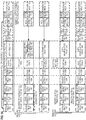
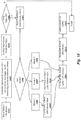
- Figures 1A-1 B are block diagrams illustrating a generic vector friendly instruction format and instruction templates thereof according to embodiments of the invention.
- Figure 1A is a block diagram illustrating a generic vector friendly instruction format and class A instruction templates thereof according to embodiments of the invention; while Figure 1B is a block diagram illustrating the generic vector friendly instruction format and class B instruction templates thereof according to embodiments of the invention.
- the term generic in the context of the vector friendly instruction format refers to the instruction format not being tied to any specific instruction set.
- a 64 byte vector operand length (or size) with 32 bit (4 byte) or 64 bit (8 byte) data element widths (or sizes) (and thus, a 64 byte vector consists of either 16 doubleword-size elements or alternatively, 8 quadword-size elements); a 64 byte vector operand length (or size) with 16 bit (2 byte) or 8 bit (1 byte) data element widths (or sizes); a 32 byte vector operand length (or size) with 32 bit (4 byte), 64 bit (8 byte), 16 bit (2 byte), or 8 bit (1 byte) data element widths (or sizes); and a 16 byte vector operand length (or size) with 32 bit (4 byte), 64 bit (8 byte), 16 bit (2 byte), or 8 bit (1 byte) data element widths (or sizes); alternative embodiments may support more, less and/or different vector operand sizes (e.g., 256 byte vector operands) with more, less, or different data
- the class A instruction templates in Figure 1A include: 1) within the no memory access 105 instruction templates there is shown a no memory access, full round control type operation 110 instruction template and a no memory access, data transform type operation 115 instruction template; and 2) within the memory access 120 instruction templates there is shown a memory access, temporal 125 instruction template and a memory access, non-temporal 130 instruction template.
- the class B instruction templates in Figure 1B include: 1) within the no memory access 105 instruction templates there is shown a no memory access, write mask control, partial round control type operation 112 instruction template and a no memory access, write mask control, vsize type operation 117 instruction template; and 2) within the memory access 120 instruction templates there is shown a memory access, write mask control 127 instruction template.
- the generic vector friendly instruction format 100 includes the following fields listed below in the order illustrated in Figures 1A-1B .
- Format field 140 - a specific value (an instruction format identifier value) in this field uniquely identifies the vector friendly instruction format, and thus occurrences of instructions in the vector friendly instruction format in instruction streams. As such, this field is optional in the sense that it is not needed for an instruction set that has only the generic vector friendly instruction format.
- Base operation field 142 its content distinguishes different base operations.
- Register index field 144 its content, directly or through address generation, specifies the locations of the source and destination operands, be they in registers or in memory. These include a sufficient number of bits to select N registers from a PxQ (e.g. 32x512, 16x128, 32x1024, 64x1024) register file. While in one embodiment N may be up to three sources and one destination register, alternative embodiments may support more or less sources and destination registers (e.g., may support up to two sources where one of these sources also acts as the destination, may support up to three sources where one of these sources also acts as the destination, may support up to two sources and one destination).
- PxQ e.g. 32x512, 16x128, 32x1024, 64x1024
- Modifier field 146 its content distinguishes occurrences of instructions in the generic vector instruction format that specify memory access from those that do not; that is, between no memory access 105 instruction templates and memory access 120 instruction templates.
- Memory access operations read and/or write to the memory hierarchy (in some cases specifying the source and/or destination addresses using values in registers), while non-memory access operations do not (e.g., the source and destinations are registers). While in one embodiment this field also selects between three different ways to perform memory address calculations, alternative embodiments may support more, less, or different ways to perform memory address calculations.
- Augmentation operation field 150 its content distinguishes which one of a variety of different operations to be performed in addition to the base operation. This field is context specific. In one embodiment of the invention, this field is divided into a class field 168, an alpha field 152, and a beta field 154. The augmentation operation field 150 allows common groups of operations to be performed in a single instruction rather than 2, 3, or 4 instructions.
- Scale field 160 - its content allows for the scaling of the index field's content for memory address generation (e.g., for address generation that uses 2 scale * index + base).
- Displacement Field 162A- its content is used as part of memory address generation (e.g., for address generation that uses 2 scale * index + base + displacement).
- Displacement Factor Field 162B (note that the juxtaposition of displacement field 162A directly over displacement factor field 162B indicates one or the other is used) - its content is used as part of address generation; it specifies a displacement factor that is to be scaled by the size of a memory access (N) - where N is the number of bytes in the memory access (e.g., for address generation that uses 2 scale * index + base + scaled displacement). Redundant low-order bits are ignored and hence, the displacement factor field's content is multiplied by the memory operands total size (N) in order to generate the final displacement to be used in calculating an effective address.
- N is determined by the processor hardware at runtime based on the full opcode field 174 (described later herein) and the data manipulation field 154C.
- the displacement field 162A and the displacement factor field 162B are optional in the sense that they are not used for the no memory access 105 instruction templates and/or different embodiments may implement only one or none of the two.
- Data element width field 164 its content distinguishes which one of a number of data element widths is to be used (in some embodiments for all instructions; in other embodiments for only some of the instructions). This field is optional in the sense that it is not needed if only one data element width is supported and/or data element widths are supported using some aspect of the opcodes.
- Write mask field 170 its content controls, on a per data element position basis, whether that data element position in the destination vector operand reflects the result of the base operation and augmentation operation.
- Class A instruction templates support merging-writemasking
- class B instruction templates support both merging- and zeroing-writemasking.
- the write mask field 170 allows for partial vector operations, including loads, stores, arithmetic, logical, etc.
- write mask field's 170 content selects one of a number of write mask registers that contains the write mask to be used (and thus the write mask field's 170 content indirectly identifies that masking to be performed), alternative embodiments instead or additional allow the mask write field's 170 content to directly specify the masking to be performed.
- Immediate field 172 - its content allows for the specification of an immediate. This field is optional in the sense that is it not present in an implementation of the generic vector friendly format that does not support immediate and it is not present in instructions that do not use an immediate.
- Class field 168 its content distinguishes between different classes of instructions. With reference to Figures 1A-B , the contents of this field select between class A and class B instructions. In Figures 1A-B , rounded corner squares are used to indicate a specific value is present in a field (e.g., class A 168A and class B 168B for the class field 168 respectively in Figures 1A-B ).
- the alpha field 152 is interpreted as an RS field 152A, whose content distinguishes which one of the different augmentation operation types are to be performed (e.g., round 152A.1 and data transform 152A.2 are respectively specified for the no memory access, round type operation 110 and the no memory access, data transform type operation 115 instruction templates), while the beta field 154 distinguishes which of the operations of the specified type is to be performed.
- the scale field 160, the displacement field 162A, and the displacement scale filed 162B are not present.
- the beta field 154 is interpreted as a round control field 154A, whose content(s) provide static rounding. While in the described embodiments of the invention the round control field 154A includes a suppress all floating point exceptions (SAE) field 156 and a round operation control field 158, alternative embodiments may support may encode both these concepts into the same field or only have one or the other of these concepts/fields (e.g., may have only the round operation control field 158).
- SAE suppress all floating point exceptions
- SAE field 156 its content distinguishes whether or not to disable the exception event reporting; when the SAE field's 156 content indicates suppression is enabled, a given instruction does not report any kind of floating-point exception flag and does not raise any floating point exception handler.
- Round operation control field 158 its content distinguishes which one of a group of rounding operations to perform (e.g., Round-up, Round-down, Round-towards-zero and Round-to-nearest).
- the round operation control field 158 allows for the changing of the rounding mode on a per instruction basis.
- the round operation control field's 150 content overrides that register value.
- the beta field 154 is interpreted as a data transform field 154B, whose content distinguishes which one of a number of data transforms is to be performed (e.g., no data transform, swizzle, broadcast).
- the alpha field 152 is interpreted as an eviction hint field 152B, whose content distinguishes which one of the eviction hints is to be used (in Figure 1A , temporal 152B.1 and non-temporal 152B.2 are respectively specified for the memory access, temporal 125 instruction template and the memory access, non-temporal 130 instruction template), while the beta field 154 is interpreted as a data manipulation field 154C, whose content distinguishes which one of a number of data manipulation operations (also known as primitives) is to be performed (e.g., no manipulation; broadcast; up conversion of a source; and down conversion of a destination).
- the memory access 120 instruction templates include the scale field 160, and optionally the displacement field 162A or the displacement scale field 162B.
- Vector memory instructions perform vector loads from and vector stores to memory, with conversion support. As with regular vector instructions, vector memory instructions transfer data from/to memory in a data element-wise fashion, with the elements that are actually transferred is dictated by the contents of the vector mask that is selected as the write mask.
- Temporal data is data likely to be reused soon enough to benefit from caching. This is, however, a hint, and different processors may implement it in different ways, including ignoring the hint entirely.
- Non-temporal data is data unlikely to be reused soon enough to benefit from caching in the 1st-level cache and should be given priority for eviction. This is, however, a hint, and different processors may implement it in different ways, including ignoring the hint entirely.
- the alpha field 152 is interpreted as a write mask control (Z) field 152C, whose content distinguishes whether the write masking controlled by the write mask field 170 should be a merging or a zeroing.
- part of the beta field 154 is interpreted as an RL field 157A, whose content distinguishes which one of the different augmentation operation types are to be performed (e.g., round 157A.1 and vector length (VSIZE) 157A.2 are respectively specified for the no memory access, write mask control, partial round control type operation 112 instruction template and the no memory access, write mask control, VSIZE type operation 117 instruction template), while the rest of the beta field 154 distinguishes which of the operations of the specified type is to be performed.
- the scale field 160, the displacement field 162A, and the displacement scale filed 162B are not present.
- Round operation control field 159A just as round operation control field 158, its content distinguishes which one of a group of rounding operations to perform (e.g., Round-up, Round-down, Round-towards-zero and Round-to-nearest).
- the round operation control field 159A allows for the changing of the rounding mode on a per instruction basis.
- the round operation control field's 150 content overrides that register value.
- the rest of the beta field 154 is interpreted as a vector length field 159B, whose content distinguishes which one of a number of data vector lengths is to be performed on (e.g., 128, 256, or 512 byte).
- part of the beta field 154 is interpreted as a broadcast field 157B, whose content distinguishes whether or not the broadcast type data manipulation operation is to be performed, while the rest of the beta field 154 is interpreted the vector length field 159B.
- the memory access 120 instruction templates include the scale field 160, and optionally the displacement field 162A or the displacement scale field 162B.
- a full opcode field 174 is shown including the format field 140, the base operation field 142, and the data element width field 164. While one embodiment is shown where the full opcode field 174 includes all of these fields, the full opcode field 174 includes less than all of these fields in embodiments that do not support all of them.
- the full opcode field 174 provides the operation code (opcode).
- the augmentation operation field 150, the data element width field 164, and the write mask field 170 allow these features to be specified on a per instruction basis in the generic vector friendly instruction format.
- write mask field and data element width field create typed instructions in that they allow the mask to be applied based on different data element widths.
- different processors or different cores within a processor may support only class A, only class B, or both classes.
- a high performance general purpose out-of-order core intended for general-purpose computing may support only class B
- a core intended primarily for graphics and/or scientific (throughput) computing may support only class A
- a core intended for both may support both (of course, a core that has some mix of templates and instructions from both classes but not all templates and instructions from both classes is within the purview of the invention).
- a single processor may include multiple cores, all of which support the same class or in which different cores support different class.
- one of the graphics cores intended primarily for graphics and/or scientific computing may support only class A, while one or more of the general purpose cores may be high performance general purpose cores with out of order execution and register renaming intended for general-purpose computing that support only class B.
- Another processor that does not have a separate graphics core may include one more general purpose in-order or out-of-order cores that support both class A and class B.
- features from one class may also be implement in the other class in different embodiments of the invention.
- Programs written in a high level language would be put (e.g., just in time compiled or statically compiled) into an variety of different executable forms, including: 1) a form having only instructions of the class(es) supported by the target processor for execution; or 2) a form having alternative routines written using different combinations of the instructions of all classes and having control flow code that selects the routines to execute based on the instructions supported by the processor which is currently executing the code.
- VEX encoding allows instructions to have more than two operands, and allows SIMD vector registers to be longer than 28 bits.
- Figure 2A illustrates an exemplary AVX instruction format including a VEX prefix 202, real opcode field 230, Mod R/M byte 240, SIB byte 250, displacement field 262, and IMM8 272.
- Figure 2B illustrates which fields from Figure 2A make up a full opcode field 274 and a base operation field 241.
- Figure 2C illustrates which fields from Figure 2A make up a register index field 244.
- VEX Prefix (Bytes 0-2) 202 is encoded in a three-byte form.
- the first byte is the Format Field 290 (VEX Byte 0, bits [7:0]), which contains an explicit C4 byte value (the unique value used for distinguishing the C4 instruction format).
- the second-third bytes (VEX Bytes 1-2) include a number of bit fields providing specific capability.
- REX field 205 (VEX Byte 1, bits [7-5]) consists of a VEX.R bit field (VEX Byte 1, bit [7] - R), VEX.X bit field (VEX byte 1, bit [6] - X), and VEX.B bit field (VEX byte 1, bit[5] - B).
- Rrrr, xxx, and bbb may be formed by adding VEX.R, VEX.X, and VEX.B.
- Opcode map field 215 (VEX byte 1, bits [4:0] - mmmmm) includes content to encode an implied leading opcode byte.
- W Field 264 (VEX byte 2, bit [7] - W) - is represented by the notation VEX.W, and provides different functions depending on the instruction.
- Real Opcode Field 230 (Byte 3) is also known as the opcode byte. Part of the opcode is specified in this field.
- MOD R/M Field 240 (Byte 4) includes MOD field 242 (bits [7-6]), Reg field 244 (bits [5-3]), and R/M field 246 (bits [2-0]).
- the role of Reg field 244 may include the following: encoding either the destination register operand or a source register operand (the rrr of Rrrr), or be treated as an opcode extension and not used to encode any instruction operand.
- the role of R/M field 246 may include the following: encoding the instruction operand that references a memory address, or encoding either the destination register operand or a source register operand.
- Scale, Index, Base (SIB) -
- the content of Scale field 250 (Byte 5) includes SS252 (bits [7-6]), which is used for memory address generation.
- the contents of SIB.xxx 254 (bits [5-3]) and SIB.bbb 256 (bits [2-0]) have been previously referred to with regard to the register indexes Xxxx and Bbbb.
- the Displacement Field 262 and the immediate field (IMM8) 272 contain data.
- Figure 3 is a block diagram of a register architecture 300 according to one embodiment of the invention.
- the lower order 256 bits of the lower 6 zmm registers are overlaid on registers ymm0-15.
- the lower order 128 bits of the lower 6 zmm registers (the lower order 128 bits of the ymm registers) are overlaid on registers xmm0-15.
- Scalar floating point stack register file (x87 stack) 345 on which is aliased the MMX packed integer flat register file 350 - in the embodiment illustrated, the x87 stack is an eight-element stack used to perform scalar floating-point operations on 32/64/80-bit floating point data using the x87 instruction set extension; while the MMX registers are used to perform operations on 64-bit packed integer data, as well as to hold operands for some operations performed between the MMX and XMM registers.
- Alternative embodiments of the invention may use wider or narrower registers. Additionally, alternative embodiments of the invention may use more, less, or different register files and registers.
- Processor cores may be implemented in different ways, for different purposes, and in different processors.
- implementations of such cores may include: 1) a general purpose in-order core intended for general-purpose computing; 2) a high performance general purpose out-of-order core intended for general-purpose computing; 3) a special purpose core intended primarily for graphics and/or scientific (throughput) computing.
- Implementations of different processors may include: 1) a CPU including one or more general purpose in-order cores intended for general-purpose computing and/or one or more general purpose out-of-order cores intended for general-purpose computing; and 2) a coprocessor including one or more special purpose cores intended primarily for graphics and/or scientific (throughput).
- Such different processors lead to different computer system architectures, which may include: 1) the coprocessor on a separate chip from the CPU; 2) the coprocessor on a separate die in the same package as a CPU; 3) the coprocessor on the same die as a CPU (in which case, such a coprocessor is sometimes referred to as special purpose logic, such as integrated graphics and/or scientific (throughput) logic, or as special purpose cores); and 4) a system on a chip that may include on the same die the described CPU (sometimes referred to as the application core(s) or application processor(s)), the above described coprocessor, and additional functionality.
- Exemplary core architectures are described next, followed by descriptions of exemplary processors and computer architectures. Detailed herein are circuits (units) that comprise exemplary cores, processors, etc.
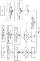
- Figure 4A is a block diagram illustrating both an exemplary in-order pipeline and an exemplary register renaming, out-of-order issue/execution pipeline according to embodiments of the invention.
- Figure 4B is a block diagram illustrating both an exemplary embodiment of an in-order architecture core and an exemplary register renaming, out-of-order issue/execution architecture core to be included in a processor according to embodiments of the invention.
- the solid lined boxes in Figures 4A-B illustrate the in-order pipeline and in-order core, while the optional addition of the dashed lined boxes illustrates the register renaming, out-of-order issue/execution pipeline and core. Given that the in-order aspect is a subset of the out-of-order aspect, the out-of-order aspect will be described.
- a processor pipeline 400 includes a fetch stage 402, a length decode stage 404, a decode stage 406, an allocation stage 408, a renaming stage 410, a scheduling (also known as a dispatch or issue) stage 412, a register read/memory read stage 414, an execute stage 416, a write back/memory write stage 418, an exception handling stage 422, and a commit stage 424.
- Figure 4B shows processor core 490 including a front end unit 430 coupled to an execution engine unit 450, and both are coupled to a memory unit 470.
- the core 490 may be a reduced instruction set computing (RISC) core, a complex instruction set computing (CISC) core, a very long instruction word (VLIW) core, or a hybrid or alternative core type.
- the core 490 may be a special-purpose core, such as, for example, a network or communication core, compression engine, coprocessor core, general purpose computing graphics processing unit (GPGPU) core, graphics core, or the like.
- GPGPU general purpose computing graphics processing unit
- the front end unit 430 includes a branch prediction unit 432 coupled to an instruction cache unit 434, which is coupled to an instruction translation lookaside buffer (TLB) 436, which is coupled to an instruction fetch unit 438, which is coupled to a decode unit 440.
- the decode unit 440 (or decoder) may decode instructions, and generate as an output one or more micro-operations, micro-code entry points, microinstructions, other instructions, or other control signals, which are decoded from, or which otherwise reflect, or are derived from, the original instructions.
- the decode unit 440 may be implemented using various different mechanisms.
- the core 490 includes a microcode ROM or other medium that stores microcode for certain macroinstructions (e.g., in decode unit 440 or otherwise within the front end unit 430).
- the decode unit 440 is coupled to a rename/allocator unit 452 in the execution engine unit 450.
- the execution engine unit 450 includes the rename/allocator unit 452 coupled to a retirement unit 454 and a set of one or more scheduler unit(s) 456.
- the scheduler unit(s) 456 represents any number of different schedulers, including reservations stations, central instruction window, etc.
- the scheduler unit(s) 456 is coupled to the physical register file(s) unit(s) 458.
- Each of the physical register file(s) units 458 represents one or more physical register files, different ones of which store one or more different data types, such as scalar integer, scalar floating point, packed integer, packed floating point, vector integer, vector floating point, status (e.g., an instruction pointer that is the address of the next instruction to be executed), etc.
- the physical register file(s) unit 458 comprises a vector registers unit and a scalar registers unit. These register units may provide architectural vector registers, vector mask registers, and general purpose registers.
- the physical register file(s) unit(s) 458 is overlapped by the retirement unit 454 to illustrate various ways in which register renaming and out-of-order execution may be implemented (e.g., using a reorder buffer(s) and a retirement register file(s); using a future file(s), a history buffer(s), and a retirement register file(s); using a register maps and a pool of registers; etc.).
- the retirement unit 454 and the physical register file(s) unit(s) 458 are coupled to the execution cluster(s) 460.
- the execution cluster(s) 460 includes a set of one or more execution units 462 and a set of one or more memory access units 464.
- the execution units 462 may perform various operations (e.g., shifts, addition, subtraction, multiplication) and on various types of data (e.g., scalar floating point, packed integer, packed floating point, vector integer, vector floating point). While some embodiments may include a number of execution units dedicated to specific functions or sets of functions, other embodiments may include only one execution unit or multiple execution units that all perform all functions.
- the scheduler unit(s) 456, physical register file(s) unit(s) 458, and execution cluster(s) 460 are shown as being possibly plural because certain embodiments create separate pipelines for certain types of data/operations (e.g., a scalar integer pipeline, a scalar floating point/packed integer/packed floating point/vector integer/vector floating point pipeline, and/or a memory access pipeline that each have their own scheduler unit, physical register file(s) unit, and/or execution cluster - and in the case of a separate memory access pipeline, certain embodiments are implemented in which only the execution cluster of this pipeline has the memory access unit(s) 464). It should also be understood that where separate pipelines are used, one or more of these pipelines may be out-of-order issue/execution and the rest in-order.
- the set of memory access units 464 is coupled to the memory unit 470, which includes a data TLB unit 472 coupled to a data cache unit 474 coupled to a level 2 (L2) cache unit 476.
- the memory access units 464 may include a load unit, a store address unit, and a store data unit, each of which is coupled to the data TLB unit 472 in the memory unit 470.
- the instruction cache unit 434 is further coupled to a level 2 (L2) cache unit 476 in the memory unit 470.
- the L2 cache unit 476 is coupled to one or more other levels of cache and eventually to a main memory.
- the exemplary register renaming, out-of-order issue/execution core architecture may implement the pipeline 400 as follows: 1) the instruction fetch 438 performs the fetch and length decoding stages 402 and 404; 2) the decode unit 440 performs the decode stage 406; 3) the rename/allocator unit 452 performs the allocation stage 408 and renaming stage 410; 4) the scheduler unit(s) 456 performs the schedule stage 412; 5) the physical register file(s) unit(s) 458 and the memory unit 470 perform the register read/memory read stage 414; the execution cluster 460 perform the execute stage 416; 6) the memory unit 470 and the physical register file(s) unit(s) 458 perform the write back/memory write stage 418; 7) various units may be involved in the exception handling stage 422; and 8) the retirement unit 454 and the physical register file(s) unit(s) 458 perform the commit stage 424.
- the core 490 may support one or more instructions sets (e.g., the x86 instruction set (with some extensions that have been added with newer versions); the MIPS instruction set of MIPS Technologies of Sunnyvale, CA; the ARM instruction set (with optional additional extensions such as NEON) of ARM Holdings of Sunnyvale, CA), including the instruction(s) described herein.
- the core 490 includes logic to support a packed data instruction set extension (e.g., AVX1, AVX2), thereby allowing the operations used by many multimedia applications to be performed using packed data.
- a packed data instruction set extension e.g., AVX1, AVX2
- the core may support multithreading (executing two or more parallel sets of operations or threads), and may do so in a variety of ways including time sliced multithreading, simultaneous multithreading (where a single physical core provides a logical core for each of the threads that physical core is simultaneously multithreading), or a combination thereof (e.g., time sliced fetching and decoding and simultaneous multithreading thereafter such as in the Intel® Hyperthreading technology).
- register renaming is described in the context of out-of-order execution, it should be understood that register renaming may be used in an in-order architecture.
- the illustrated embodiment of the processor also includes separate instruction and data cache units 434/474 and a shared L2 cache unit 476, alternative embodiments may have a single internal cache for both instructions and data, such as, for example, a Level 1 (L1) internal cache, or multiple levels of internal cache.
- the system may include a combination of an internal cache and an external cache that is external to the core and/or the processor. Alternatively, all of the cache may be external to the core and/or the processor.
- Figures 5A-B illustrate a block diagram of a more specific exemplary in-order core architecture, which core would be one of several logic blocks (including other cores of the same type and/or different types) in a chip.
- the logic blocks communicate through a high-bandwidth interconnect network (e.g., a ring network) with some fixed function logic, memory I/O interfaces, and other necessary I/O logic, depending on the application.
- a high-bandwidth interconnect network e.g., a ring network
- Figure 5A is a block diagram of a single processor core, along with its connection to the on-die interconnect network 502 and with its local subset of the Level 2 (L2) cache 504, according to embodiments of the invention.
- an instruction decoder 500 supports the x86 instruction set with a packed data instruction set extension.
- An L1 cache 506 allows low-latency accesses to cache memory into the scalar and vector units.
- a scalar unit 508 and a vector unit 510 use separate register sets (respectively, scalar registers 512 and vector registers 514) and data transferred between them is written to memory and then read back in from a level 1 (L1) cache 506, alternative embodiments of the invention may use a different approach (e.g., use a single register set or include a communication path that allow data to be transferred between the two register files without being written and read back).
- the local subset of the L2 cache 504 is part of a global L2 cache that is divided into separate local subsets, one per processor core. Each processor core has a direct access path to its own local subset of the L2 cache 504. Data read by a processor core is stored in its L2 cache subset 504 and can be accessed quickly, in parallel with other processor cores accessing their own local L2 cache subsets. Data written by a processor core is stored in its own L2 cache subset 504 and is flushed from other subsets, if necessary.
- the ring network ensures coherency for shared data. The ring network is bi-directional to allow agents such as processor cores, L2 caches and other logic blocks to communicate with each other within the chip. Each ring data-path is 1024-bits wide per direction in some embodiments.
- Figure 5B is an expanded view of part of the processor core in Figure 5A according to embodiments of the invention.
- Figure 5B includes an L1 data cache 506A part of the L1 cache 504, as well as more detail regarding the vector unit 510 and the vector registers 514.
- the vector unit 510 is a 6-wide vector processing unit (VPU) (see the 16-wide ALU 528), which executes one or more of integer, single-precision float, and double-precision float instructions.
- the VPU supports swizzling the register inputs with swizzle unit 520, numeric conversion with numeric convert units 522A-B, and replication with replication unit 524 on the memory input.
- Figure 6 is a block diagram of a processor 600 that may have more than one core, may have an integrated memory controller, and may have integrated graphics according to embodiments of the invention.
- the solid lined boxes in Figure 6 illustrate a processor 600 with a single core 602A, a system agent 610, a set of one or more bus controller units 616, while the optional addition of the dashed lined boxes illustrates an alternative processor 600 with multiple cores 602A-N, a set of one or more integrated memory controller unit(s) 614 in the system agent unit 610, and special purpose logic 608.
- different implementations of the processor 600 may include: 1) a CPU with the special purpose logic 608 being integrated graphics and/or scientific (throughput) logic (which may include one or more cores), and the cores 602A-N being one or more general purpose cores (e.g., general purpose in-order cores, general purpose out-of-order cores, a combination of the two); 2) a coprocessor with the cores 602A-N being a large number of special purpose cores intended primarily for graphics and/or scientific (throughput); and 3) a coprocessor with the cores 602A-N being a large number of general purpose in-order cores.
- the special purpose logic 608 being integrated graphics and/or scientific (throughput) logic
- the cores 602A-N being one or more general purpose cores (e.g., general purpose in-order cores, general purpose out-of-order cores, a combination of the two)
- a coprocessor with the cores 602A-N being a large number of special purpose core
- the processor 600 may be a general-purpose processor, coprocessor or special-purpose processor, such as, for example, a network or communication processor, compression engine, graphics processor, GPGPU (general purpose graphics processing unit), a high-throughput many integrated core (MIC) coprocessor (including 30 or more cores), embedded processor, or the like.
- the processor may be implemented on one or more chips.
- the processor 600 may be a part of and/or may be implemented on one or more substrates using any of a number of process technologies, such as, for example, BiCMOS, CMOS, or NMOS.
- the memory hierarchy includes one or more levels of cache within the cores 604A-N, a set or one or more shared cache units 606, and external memory (not shown) coupled to the set of integrated memory controller units 614.
- the set of shared cache units 606 may include one or more mid-level caches, such as level 2 (L2), level 3 (L3), level 4 (L4), or other levels of cache, a last level cache (LLC), and/or combinations thereof. While in one embodiment a ring based interconnect unit 612 interconnects the integrated graphics logic 608, the set of shared cache units 606, and the system agent unit 610/integrated memory controller unit(s) 614, alternative embodiments may use any number of well-known techniques for interconnecting such units. In one embodiment, coherency is maintained between one or more cache units 606 and cores 602-AN.
- the system agent 610 includes those components coordinating and operating cores 602A-N.
- the system agent unit 610 may include for example a power control unit (PCU) and a display unit.
- the PCU may be or include logic and components needed for regulating the power state of the cores 602A-N and the integrated graphics logic 608.
- the display unit is for driving one or more externally connected displays.
- the cores 602A-N may be homogenous or heterogeneous in terms of architecture instruction set; that is, two or more of the cores 602A-N may be capable of execution the same instruction set, while others may be capable of executing only a subset of that instruction set or a different instruction set.
- Figures 7-10 are block diagrams of exemplary computer architectures.
- Other system designs and configurations known in the arts for laptops, desktops, handheld PCs, personal digital assistants, engineering workstations, servers, network devices, network hubs, switches, embedded processors, digital signal processors (DSPs), graphics devices, video game devices, set-top boxes, micro controllers, cell phones, portable media players, hand held devices, and various other electronic devices, are also suitable.
- DSPs digital signal processors
- graphics devices video game devices, set-top boxes, micro controllers, cell phones, portable media players, hand held devices, and various other electronic devices, are also suitable.
- DSPs digital signal processors
- a huge variety of systems or electronic devices capable of incorporating a processor and/or other execution logic as disclosed herein are generally suitable.
- the system 700 may include one or more processors 710, 715, which are coupled to a controller hub 720.
- the controller hub 720 includes a graphics memory controller hub (GMCH) 790 and an Input/Output Hub (IOH) 750 (which may be on separate chips);
- the GMCH 790 includes memory and graphics controllers to which are coupled memory 740 and a coprocessor 745;
- the IOH 750 is couples input/output (I/O) devices 760 to the GMCH 790.
- the memory and graphics controllers are integrated within the processor (as described herein), the memory 740 and the coprocessor 745 are coupled directly to the processor 710, and the controller hub 720 in a single chip with the IOH 750.
- processors 715 may include one or more of the processing cores described herein and may be some version of the processor 600.
- the memory 740 may be, for example, dynamic random access memory (DRAM), phase change memory (PCM), or a combination of the two.
- the controller hub 720 communicates with the processor(s) 710, 715 via a multi-drop bus, such as a frontside bus (FSB), point-to-point interface, or similar connection 795.
- a multi-drop bus such as a frontside bus (FSB), point-to-point interface, or similar connection 795.
- the coprocessor 745 is a special-purpose processor, such as, for example, a high-throughput MIC processor, a network or communication processor, compression engine, graphics processor, GPGPU, embedded processor, or the like.
- controller hub 720 may include an integrated graphics accelerator.
- the processor 710 executes instructions that control data processing operations of a general type. Embedded within the instructions may be coprocessor instructions. The processor 710 recognizes these coprocessor instructions as being of a type that should be executed by the attached coprocessor 745. Accordingly, the processor 710 issues these coprocessor instructions (or control signals representing coprocessor instructions) on a coprocessor bus or other interconnect, to coprocessor 745. Coprocessor(s) 745 accept and execute the received coprocessor instructions.
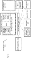
- multiprocessor system 800 is a point-to-point interconnect system, and includes a first processor 870 and a second processor 880 coupled via a point-to-point interconnect 850.
- processors 870 and 880 may be some version of the processor 600.
- processors 870 and 880 are respectively processors 710 and 715, while coprocessor 838 is coprocessor 745.
- processors 870 and 880 are respectively processor 710 coprocessor 745.
- Processors 870 and 880 are shown including integrated memory controller (IMC) units 872 and 882, respectively.
- Processor 870 also includes as part of its bus controller units point-to-point (P-P) interfaces 876 and 878; similarly, second processor 880 includes P-P interfaces 886 and 888.
- Processors 870, 880 may exchange information via a point-to-point (P-P) interface 850 using P-P interface circuits 878, 888.
- IMCs 872 and 882 couple the processors to respective memories, namely a memory 832 and a memory 834, which may be portions of main memory locally attached to the respective processors.
- Processors 870, 880 may each exchange information with a chipset 890 via individual P-P interfaces 852, 854 using point to point interface circuits 876, 894, 886, 898.
- Chipset 890 may optionally exchange information with the coprocessor 838 via a high-performance interface 892.
- the coprocessor 838 is a special-purpose processor, such as, for example, a high-throughput MIC processor, a network or communication processor, compression engine, graphics processor, GPGPU, embedded processor, or the like.
- a shared cache (not shown) may be included in either processor or outside of both processors, yet connected with the processors via P-P interconnect, such that either or both processors' local cache information may be stored in the shared cache if a processor is placed into a low power mode.
- first bus 816 may be a Peripheral Component Interconnect (PCI) bus, or a bus such as a PCI Express bus or another I/O interconnect bus, although the scope of the present invention is not so limited.
- PCI Peripheral Component Interconnect
- various I/O devices 814 may be coupled to first bus 816, along with a bus bridge 818 which couples first bus 816 to a second bus 820.
- one or more additional processor(s) 815 such as coprocessors, high-throughput MIC processors, GPGPU's, accelerators (such as, e.g., graphics accelerators or digital signal processing (DSP) units), field programmable gate arrays, or any other processor, are coupled to first bus 816.
- second bus 820 may be a low pin count (LPC) bus.
- Various devices may be coupled to a second bus 820 including, for example, a keyboard and/or mouse 822, communication devices 827 and a storage unit 828 such as a disk drive or other mass storage device which may include instructions/code and data 830, in one embodiment.
- a storage unit 828 such as a disk drive or other mass storage device which may include instructions/code and data 830, in one embodiment.
- an audio I/O 824 may be coupled to the second bus 816.
- a system may implement a multi-drop bus or other such architecture.
- FIG. 9 shown is a block diagram of a second more specific exemplary system 900 in accordance with an embodiment of the present invention.
- Like elements in Figures 8 and 9 bear like reference numerals, and certain aspects of Figure 8 have been omitted from Figure 9 in order to avoid obscuring other aspects of Figure 9 .
- FIG 9 illustrates that the processors 870, 880 may include integrated memory and I/O control logic ("CL") 972 and 982, respectively.
- CL I/O control logic
- the CL 972, 982 include integrated memory controller units and include I/O control logic.
- Figure 9 illustrates that not only are the memories 832, 834 coupled to the CL 872, 882, but also that I/O devices 914 are also coupled to the control logic 872, 882.
- Legacy I/O devices 915 are coupled to the chipset 890.
- an interconnect unit(s) 1002 is coupled to: an application processor 1010 which includes a set of one or more cores 102A-N, cache units 604A-N, and shared cache unit(s) 606; a system agent unit 610; a bus controller unit(s) 616; an integrated memory controller unit(s) 614; a set or one or more coprocessors 1020 which may include integrated graphics logic, an image processor, an audio processor, and a video processor; an static random access memory (SRAM) unit 1030; a direct memory access (DMA) unit 1032; and a display unit 1040 for coupling to one or more external displays.
- the coprocessor(s) 1020 include a special-purpose processor, such as, for example, a network
- Embodiments of the mechanisms disclosed herein may be implemented in hardware, software, firmware, or a combination of such implementation approaches.
- Embodiments of the invention may be implemented as computer programs or program code executing on programmable systems comprising at least one processor, a storage system (including volatile and nonvolatile memory and/or storage elements), at least one input device, and at least one output device.
- Program code such as code 830 illustrated in Figure 8
- Program code 830 illustrated in Figure 8 may be applied to input instructions to perform the functions described herein and generate output information.
- the output information may be applied to one or more output devices, in known fashion.
- a processing system includes any system that has a processor, such as, for example; a digital signal processor (DSP), a microcontroller, an application specific integrated circuit (ASIC), or a microprocessor.
- DSP digital signal processor
- ASIC application specific integrated circuit
- the program code may be implemented in a high level procedural or object oriented programming language to communicate with a processing system.
- the program code may also be implemented in assembly or machine language, if desired.
- the mechanisms described herein are not limited in scope to any particular programming language. In any case, the language may be a compiled or interpreted language.
- IP cores may be stored on a tangible, machine readable medium and supplied to various customers or manufacturing facilities to load into the fabrication machines that actually make the logic or processor.
- Such machine-readable storage media may include, without limitation, non-transitory, tangible arrangements of articles manufactured or formed by a machine or device, including storage media such as hard disks, any other type of disk including floppy disks, optical disks, compact disk read-only memories (CD-ROMs), compact disk rewritable's (CD-RWs), and magneto-optical disks, semiconductor devices such as read-only memories (ROMs), random access memories (RAMs) such as dynamic random access memories (DRAMs), static random access memories (SRAMs), erasable programmable read-only memories (EPROMs), flash memories, electrically erasable programmable read-only memories (EEPROMs), phase change memory (PCM), magnetic or optical cards, or any other type of media suitable for storing electronic instructions.
- storage media such as hard disks, any other type of disk including floppy disks, optical disks, compact disk read-only memories (CD-ROMs), compact disk rewritable's (CD-RWs), and magneto
- embodiments of the invention also include non-transitory, tangible machine-readable media containing instructions or containing design data, such as Hardware Description Language (HDL), which defines structures, circuits, apparatuses, processors and/or system features described herein.
- HDL Hardware Description Language
- Such embodiments may also be referred to as program products.
- Emulation including binary translation, code morphing, etc.
- an instruction converter may be used to convert an instruction from a source instruction set to a target instruction set.
- the instruction converter may translate (e.g., using static binary translation, dynamic binary translation including dynamic compilation), morph, emulate, or otherwise convert an instruction to one or more other instructions to be processed by the core.
- the instruction converter may be implemented in software, hardware, firmware, or a combination thereof.
- the instruction converter may be on processor, off processor, or part on and part off processor.
- Figure 11 is a block diagram contrasting the use of a software instruction converter to convert binary instructions in a source instruction set to binary instructions in a target instruction set according to embodiments of the invention.
- the instruction converter is a software instruction converter, although alternatively the instruction converter may be implemented in software, firmware, hardware, or various combinations thereof.
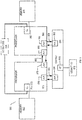
- Figure 11 shows a program in a high level language 1102 may be compiled using an first compiler 1104 to generate a first binary code (e.g., x86) 1106 that may be natively executed by a processor with at least one first instruction set core 1116.
- a first binary code e.g., x86
- the processor with at least one first instruction set core 1116 represents any processor that can perform substantially the same functions as an Intel processor with at least one x86 instruction set core by compatibly executing or otherwise processing (1) a substantial portion of the instruction set of the Intel x86 instruction set core or (2) object code versions of applications or other software targeted to run on an Intel processor with at least one x86 instruction set core, in order to achieve substantially the same result as an Intel processor with at least one x86 instruction set core.
- the first compiler 1104 represents a compiler that is operable to generate binary code of the first instruction set 1106 (e.g., object code) that can, with or without additional linkage processing, be executed on the processor with at least one first instruction set core 1116.
- Figure 11 shows the program in the high level language 1102 may be compiled using an alternative instruction set compiler 1108 to generate alternative instruction set binary code 1110 that may be natively executed by a processor without at least one first instruction set core 1114 (e.g., a processor with cores that execute the MIPS instruction set of MIPS Technologies of Sunnyvale, CA and/or that execute the ARM instruction set of ARM Holdings of Sunnyvale, CA).
- the instruction converter 1112 is used to convert the first binary code 1106 into code that may be natively executed by the processor without an first instruction set core 1114.
- the instruction converter 1112 represents software, firmware, hardware, or a combination thereof that, through emulation, simulation or any other process, allows a processor or other electronic device that does not have a first instruction set processor or core to execute the first binary code 1106.
- the ASAP is configured at the L2 cache and is co-optimized for timeliness, coverage and area.
- processors will have both L1 and L2 prefetchers (to prefetch for L1 and L2 caches, respectively).
- the L1 prefetchers usually operate on program virtual addresses and instruction pointers (IPs) and aim to prefetch data from outer cache levels such as the L2 or LLC into the L1 in time for the processor loads.
- IPs instruction pointers
- the L2 prefetchers operate on physical addresses (since the TLBs storing virtual-to-physical address translations are at the level of the L1) which attempt to prefetch long latency memory accesses into the larger L2/LLC caches.
- Pertinent metrics for prefetching include Coverage, Accuracy, and Timeliness.
- Coverage indicates the extent to which accesses are correctly predicted by the prefetcher and may be expressed as a ratio of correct predictions over total accesses made by the program. This represents the number of higher latency accesses saved by the prefetcher.
- Accuracy may be expressed as a ratio of accesses correctly predicted / accesses incorrectly predicted. Incorrectly predicted addresses cause cache pollution and increased pressure on the memory subsystem resources (e.g., bandwidth).
- Timeliness defines the extent to which prefetches are performed sufficiently in advance of when the data is requested. Timeliness may be enhanced by early triggering of prefetches at a large "distance" from the triggering access, saving/hiding a large portion of the high latency to memory and may have a significant impact on performance.
- the goal would be to predict all the correct/relevant accesses to the page (maximizing coverage and accuracy) on the first access seen to the page at the L2 cache (maximizing timeliness). Moreover, this needs to be achieved under reasonable area/resource requirements of the prefetcher to enable efficient, high speed implementations. This requirement is directly addressed by the embodiments of the invention, including the ASAP prefetcher described herein.
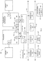
- FIG. 12 illustrates an example processor architecture on which embodiments of the invention may be implemented.
- core 1201a includes an L2 prefetcher 1207 which implements the techniques described herein to prefetch data to the L2 cache 1213.
- the illustrated architecture includes a core region 1201 and a shared or "uncore" region 1210.
- the shared region 1210 includes data structures and circuitry shared by all or a subset of the cores 1201a-b.
- the plurality of cores 1201a-b are simultaneous multithreaded cores capable of concurrently executing multiple instruction streams or threads.
- the core region 1201 may include any number of cores, each of which may include the same architecture as shown for Core 1201a.
- Another embodiment includes heterogeneous cores (e.g., low power cores combined with high power/performance cores).
- the various components illustrated in Figure 12 may be implemented in the same manner as corresponding components in Figures 1-11 .
- the core 1201a may execute instructions using one of the instruction formats in Figures 1a-b and 2a-c , and/or using the register architecture illustrated in Figure 3 .
- the cores 1201a may include the components of core 490 shown in Figure 4b , and may include any of the processor/core components described herein (e.g., Figures 5a-b , Figure 6 , etc).
- Each of the cores 1201a-b include instruction pipeline components for performing simultaneous, out-of-order (or in-order) execution of instruction streams including instruction fetch circuitry 1218 which fetches instructions from system memory 1260 or the L1 instruction cache 1210 and decode circuitry 1209 which decodes the instructions.
- Instruction fetch circuitry 1218 which fetches instructions from system memory 1260 or the L1 instruction cache 1210
- decode circuitry 1209 which decodes the instructions.
- Execution circuitry 1208 executes the decoded instructions to perform the underlying operations, as specified by the instruction operands, opcodes, and any immediate values.
- GPRs 1218d general purpose registers
- a set of vector registers 1218b a set of mask registers 1218a
- a set of control registers 1218c a set of control registers 1218c.
- multiple vector data elements are packed into each vector register 1206 which may have a 512 bit width for storing two 256 bit values, four 128 bit values, eight 64 bit values, sixteen 32 bit values, etc.
- the mask registers 1207 include eight 64-bit operand mask registers used for performing bit masking operations on the values stored in the vector registers 1206 (e.g., implemented as mask registers k0-k7 described above).
- the underlying principles of the invention are not limited to any particular mask register size/type.
- the control registers 1218c store various types of control bits or "flags" which are used by executing instructions to determine the current state of the processor core 1201a.
- the control registers include the EFLAGS register.
- An interconnect 1206 such as an on-die interconnect (IDI) implementing an IDI/coherence protocol communicatively couples the cores 1201a-b (and potentially an MPU accelerator 1201d) to one another and to various components within the shared region 1210.
- IDI on-die interconnect
- the interconnect 1206 couples core 1201a via interface 1207 to a level 3 (L3) cache and an integrated memory controller 1230 which couples the processor to a system memory 1260.
- L3 level 3
- the integrated memory controller 1230 provides access to a system memory 1260 when performing memory operations (e.g., such as a MOV from system memory 1260 to a register).
- memory operations e.g., such as a MOV from system memory 1260 to a register.
- One or more input/output (I/O) circuits such as PCI express circuitry may also be included in the shared region 1210.
- An instruction pointer register 1212 stores an instruction pointer address identifying the next instruction to be fetched, decoded, and executed. Instructions may be fetched or prefetched from system memory 1260 and/or one or more shared cache levels such as an L2 cache 1213, the shared L3 cache 1220, or the L1 instruction cache 1210. In addition, an L1 data cache 1202 stores data loaded from system memory 1260 and/or retrieved from one of the other cache levels 1213, 1220 which cache both instructions and data.
- An instruction TLB (ITLB) 1211 stores virtual address to physical address translations for the instructions fetched by the fetch circuitry 1218 and a data TLB (DTLB) 1203 stores virtual-to-physical address translations for the data processed by the decode circuitry 1209 and execution circuitry 1208.
- Figure 12 also illustrates a branch prediction unit 1221 for speculatively predicting instruction branch addresses and branch target buffers (BTBs) 1222 for storing branch addresses and target addresses.
- BTBs branch target buffers
- a branch history table (not shown) or other data structure is maintained and updated for each branch prediction/misprediction and is used by the branch prediction unit 1202 to make subsequent branch predictions.
- Figure 12 is not intended to provide a comprehensive view of all circuitry and interconnects employed within a processor. Rather, components which are not pertinent to the embodiments of the invention are not shown. Conversely, some components are shown merely for the purpose of providing an example architecture in which embodiments of the invention may be implemented.
- Prefetchers with the highest impact and relevant for comparison with ASAP are: the Streamer Prefetcher, Spatial Memory Streamer (SMS), and Signature Path Prefetch (SPP).
- SMS Spatial Memory Streamer
- SPP Signature Path Prefetch
- the Streamer Prefetcher looks for a directional trend and issues prefetches a fixed distance (8 or 16 cachelines) away from the triggering access. It does not efficiently capture non-uniform (non-streaming) access patterns to a page and is highly inaccurate in a number of cases. SMS associates a signature (triggering PC and offset to a page) with an entire 64 bit pattern of subsequent accesses to the page. While more accurate and timely than Streamer prefetchers, SMS still has some major drawbacks related to area and coverage/accuracy.
- the SPP is the current L2 prefetcher capable of dealing with complex non-uniform access patterns in a page. Timeliness of prefetches however is limited. Without the use of a triggering PC, it has a limited mechanism for triggering prefetches on the first access to the page. It achieves prefetch distance on subsequent accesses through a series of recursive predictions, each of lower confidence or accuracy, finally bound by a lower limit on confidence. This again puts a limit on prefetch timeliness
- L2 prefetcher 1207 optimizes timeliness, coverage, accuracy and area for physical address prefetching at the L2 cache 1213.
- storage requirements of data patterns are decoupled from signatures, resulting in significant storage savings which can be fed back into increasing coverage and timeliness.
- the L2 prefetcher 1207 simultaneously optimizes both timeliness and coverage since prefetches to all subsequent accesses in a page are generated at the earliest of multiple trigger points.
- the invention achieves this by judiciously and systematically compressing prefetch patterns from a 64B granularity (for predicted cachelines) to some multiple of 64B, such as a 128B granularity (e.g., predicting 2 consecutive cachelines) or a 256B granularity (e.g., using a 16b pattern).
- the signature stores a 2-bit mode to decode the granularity of the prediction.
- 128B granularity for example, a 64b pattern is compressed to a 32b pattern, represented by 2*8b pattern bank index.
- the underlying principles of the invention are not limited to 64B and multiples thereof. For example, in unclaimed examples, prefetches using 8B, 16B, 32B, and multiples thereof may be used.
- a granularity selector 1305 determines the current granularity to be used for prefetching by the ASAP 1207 based on hit rates for one or more prefetch pattern banks 1301-1302.
- the prefetch pattern banks include a 64B prefetch pattern bank 1301 and a 128B pattern bank 1302, each with 256 entries.
- the underlying principles of the invention are not limited to any specific number of bytes or entries.
- each of the two pattern banks 1301-1302 are organized as a 32 set, 8 way associative structure.
- the 64B pattern bank 1301 may store 32b patterns and the 128B pattern bank 1302 may store 32b patterns compressed into a 16b pattern.
- One embodiment of the ASAP prefetcher 1207 also includes a 64-entry page buffer 1310 organized as a first-in-first-out (FIFO) buffer and indexed by the physical page address (PPA) 1311.
- This structure includes an accumulation vector 1320 which, in one embodiment is a 64-bit vector that accumulates the pattern of accesses seen in each page.
- IP triggering instruction pointer
- a plurality of prediction tables 1303A-D are used in one embodiment, each of which includes 18bits of data to index one of the prefetch pattern banks 1301-1302.
- the next 16 bits identify the pattern and may be used as an index to the identified prefetch pattern bank 1301-1302. For 64B granularity, for example, this may include two 8b indices into the 64B prefetch pattern bank 1301 and for 128B granularity, this may include two 8b indices into the 128B prefetch pattern bank 1302. If a 256B prefetch pattern bank is used, a 16b direct compressed pattern may be used.
- the adaptive spatial access prefetcher 1207 uses the following four tables, each of which are set associative with 16 ways (with sets determined by the size):
- the illustrated embodiment includes a prefetch buffer 1355 for storing two 64b bit-vectors for generated and issued prefetches for cache lines prefetched from the memory subsystem 1360 and stored in the L2 cache 1213 under the control of the prefetch circuitry 1350.
- a granularity selector 1305 controls the granularity at which cache lines are prefetched in response to hit rates of each of the prefetch pattern banks 1301-1302.
- the prefetch buffer 1355 includes 16 entries, although the underlying principles of the invention are not limited to any particular number of prefetch buffer entries.
- FIG. 14 A process in accordance with one embodiment of the invention is illustrated in Figure 14 .
- the process may be implemented on the architectures described above but is not limited to any particular processor or system architecture.
- a new read to the L2 cache performs a lookup in the page buffer. If the page is already in the page buffer, determined at 1402, the page buffer entry is updated at 1403 (i.e., the 64b bit-vector, offsets into the page, etc). As mentioned, the first six accesses make predictions. Thus, if within the first six accesses, determined at 1404, then the pattern prediction is performed at 1405 (a detailed embodiment is shown in Figure 15 ). If the page is not in the page buffer at 1402, then it is inserted into the page buffer at 1406. Insertion into the page buffer can result in an eviction for another page, determined at 1407. In response to an eviction, the pattern bank and prediction tables are updated at 1408 (with a detailed embodiment illustrated in Figure 16 ). For example, the evicted entry may use its 64b bit vector and offsets to update the pattern banks and prediction tables.
- Figure 15 illustrates an exemplary method for pattern prediction.
- a signature for access is generated at 1502.
- the first two accesses may use the triggering program counter (PC) value (e.g., the address of the instruction triggering the operation), while the remaining accesses also use deltas between offsets (as previously described).
- PC program counter
- a appropriate prediction table is indexed at 1503 (e.g., one of the prediction tables 1303A-D).
- the prediction table is read to identify the particular mode and prefetch pattern bank to be used (e.g., one of the 64B, 128B, 256B pattern banks for Modes 1, 2, and 3, respectively) and the pattern bank index to identify an entry in the selected pattern bank.
- the end result is a 64b spatial pattern of accesses at 1511, which may be rotated left by a first offset number of bits at 1512 and added to the prediction buffer at 1514 (i.e., to be used by prefetch circuitry to prefetch cache lines based on the pattern of accesses).
- Figure 16 illustrates one embodiment of a method for updating one of the pattern banks in response to a page buffer eviction (e.g., at 1408 in Figure 14 ).
- the 64b bit-vector is rotated right by a first offset number of bits at 1602.
- the 64b bit vector is split into two 32b portions at 1603 and a lookup is performed on the 64B pattern bank using both 32b values at 1605, resulting in 2*8b or 16b value.
- the 64b bit vector is compressed to 32b and the 32b vale is split into two 16b values. portions at 1603 and a lookup is performed on the 64B pattern bank using both 32b values at 1605, resulting in 2*8b or a 16b value.
- the final 16b value is generated from Mode 1 at 1609, depending on whether there is a replacement in the 64B pattern bank at 1607. Similarly, the final 16b value is generated from Mode 2 at 1610, depending on whether there is a replacement in the 128B pattern bank at 1608. Depending on the outcome, a Mode 3 64b bit vector for the 256B granularity pattern bank is compressed to 16b at 1611.
- a final 16b value is produced at 1612 and signatures are generated at 1613.
- the first two accesses may use the triggering PC value and the remaining accesses may use deltas between offsets.
- a lookup using the signature is performed to the appropriate prediction/signature tables and the signature is updated (or inserted for a miss) with the 16b signature and 2b mode value.
- the ASAP prefetcher 1207 achieves a significant increase in processor performance over current prefetchers in both industry and academia.
- One embodiment has been modeled in a cycle accurate research simulator, across a wide variety of workload categories (all of SPEC, a range of client (Sysmark, Apple) and Server (TPCC, Enterprise, workstation) workloads we see an average 2% (and up to 45%) increase in single thread performance over SPP and an average of 4.15% (up to 45%) increase in performance over SMS.
- the ASAP prefetcher 1207 provides an average 1.3% increase in multi-thread performance over SPP and a 5.6% increase in multi-thread performance over SMS for SPEC workloads.
- the prefetching techniques described herein are 0.5% more accurate than SPP (Percentage of fills into L2 by the prefetcher that see subsequent demand hits). With a novel decoupling of patterns and signature, ASAP achieves this performance/accuracy with around 10KB of storage at the L2.
- Figure 17 illustrates a characterization of patterns seen in example workloads.
- 1024 patterns are needed to cover an average 90% of all the patterns seen within a 10 million instruction window.
- a 64b pattern is composed from two 32b patterns, the top 256 32b patterns cover over 90% of all 32b patterns.
- 64 16b patterns cover 90% of all 16b patterns.
- the top 256 patterns are stored in a 256 entry pattern bank (32 sets / 8 way set associative). This allows the 32b pattern to be represented as an 8 bit index, leading to a 75% reduction in storage of patterns as indicated in Figure 18 (showing a reduction in pattern storage area with a Pattern Bank).
- Performance is achieved by triggering prefetches at the earliest possible point (not necessarily the first) and with the simplest signature. Performance is a function of both coverage and timeliness. SMS uses a signature of triggering PC and first offset to predict the spatial access pattern to a page. SPP uses a signature of the last 4 deltas seen in accesses to a page to predict future accesses to a page.
- Triggering prefetches on the first possible access provides maximum timeliness. But if prefetches are not triggered on the first access, there is no mechanism to trigger prefetches on subsequent accesses.
- Figure 21 shows cumulative increase in coverage when triggering prefetches from more accesses.
- the ASAP prefetcher 1207 described herein meets a balance between coverage and accuracy. When it is possible to be accurate when maintaining high coverage, it is accurate. But it is also able to tradeoff accuracy for increased coverage when coverage is poor.
- the embodiments of the invention achieve this by judiciously/systematically compressing patterns from a 64B granularity (predicting cachelines) to a 128B granularity (predicting 2 consecutive cachelines; 64b pattern compressed to 32b pattern, again represented by 2*8b pattern bank index) and finally (if needed) a 256B granularity (16b pattern).
- the signature stores a 2-bit mode to decode the granularity of the prediction.
- the selection of the granularity of prefetch is based on the pattern bank hit rates in the 64B pattern bank (256 entries) and the 128B pattern bank (256 entries). Further optimizations for this are contemplated for additional embodiments of the invention. Different comparisons of performance and accuracy are graphed in Figures 22-24 .
- Table 1 illustrates exemplary storage calculations for an implementation of the ASAP prefetcher 1207 described herein. Note that these values are provide merely for the purpose of illustration. The underlying principles of the invention are not limited to these or any specific set of values.
- embodiments of the invention achieve a significant increase in processor performance over the current state of the art prefetchers.
- Embodiments of the invention may include various steps, which have been described above.
- the steps may be embodied in machine-executable instructions which may be used to cause a general-purpose or special-purpose processor to perform the steps.
- these steps may be performed by specific hardware components that contain hardwired logic for performing the steps, or by any combination of programmed computer components and custom hardware components.
Description
- The embodiments of the invention relate generally to the field of computer processors. More particularly, the embodiments relate to an adaptive spatial access prefetcher apparatus and method.
- An instruction set, or instruction set architecture (ISA), is the part of the computer architecture related to programming, including the native data types, instructions, register architecture, addressing modes, memory architecture, interrupt and exception handling, and external input and output (I/O). It should be noted that the term "instruction" generally refers herein to macro-instructions - that is instructions that are provided to the processor for execution - as opposed to micro-instructions or micro-ops - that is the result of a processor's decoder decoding macro-instructions. The micro-instructions or micro-ops can be configured to instruct an execution unit on the processor to perform operations to implement the logic associated with the macro-instruction.
- The ISA is distinguished from the microarchitecture, which is the set of processor design techniques used to implement the instruction set. Processors with different microarchitectures can share a common instruction set. For example, Intel® Pentium 4 processors, Intel® Core™ processors, and processors from Advanced Micro Devices, Inc. of Sunnyvale CA implement nearly identical versions of the x86 instruction set (with some extensions that have been added with newer versions), but have different internal designs. For example, the same register architecture of the ISA may be implemented in different ways in different microarchitectures using well-known techniques, including dedicated physical registers, one or more dynamically allocated physical registers using a register renaming mechanism (e.g., the use of a Register Alias Table (RAT), a Reorder Buffer (ROB) and a retirement register file). Unless otherwise specified, the phrases register architecture, register file, and register are used herein to refer to that which is visible to the software/programmer and the manner in which instructions specify registers. Where a distinction is required, the adjective "logical," "architectural," or "software visible" will be used to indicate registers/files in the register architecture, while different adjectives will be used to designate registers in a given microarchitecture (e.g., physical register, reorder buffer, retirement register, register pool).
-
US 2018/089087 A1 relates to an improved flash-based memory module, and a method of operating the same. A method of storing data in a memory module including an in-module prefetcher, an in-module prefetch buffer, memory, and a memory controller, the method including sending address information from the in-module prefetcher to the memory controller and to the prefetch buffer, determining prefetch accuracy based on a comparison of the address information sent to the memory controller and the address information sent to the prefetch buffer, determining a prefetch mode based on the prefetch accuracy, and storing the data in the memory based on the prefetch mode. -
EP 3 285 172 A1 relates to a data cache region prefetcher creating a region when a data cache miss occurs. Each region includes a predetermined range of data lines proximate to each data cache miss and is tagged with an associated instruction pointer register (RIP). The data cache region prefetcher compares subsequent memory requests against the predetermined range of data lines for each of the existing regions. For each match, the data cache region prefetcher sets an access bit and attempts to identify a pseudo-random access pattern based on the set access bits. The data cache region prefetcher increments or decrements appropriate counters to track how often the pseudo-random access pattern occurs. If the pseudo-random access pattern occurs frequently, then the next time a memory request is processed with the same RIP and pattern, the data cache region prefetcher prefetches the data lines in accordance with the pseudo-random access pattern for that RIP. - MANJUNATH SHEVGOOR ET AL, "Efficiently prefetching complex address patterns", PROCEEDINGS OF THE 48TH INTERNATIONAL SYMPOSIUM ON MICROARCHITECTURE, MICRO-48, New York, New York, USA, and Bera, "Adaptive Prefetch Filter to Mitigate Prefetcher Induced Pollution", URL: https://cse.iitk.ac.in/users/rbera/docs/thesis.pdf, also relate to techniques for efficiently prefetching.
- The present invention is defined in the independent claims. The dependent claims define embodiments thereof.
- A better understanding of the present invention can be obtained from the following detailed description in conjunction with the following drawings, in which:
-
FIGS. 1A and1B are block diagrams illustrating a generic vector friendly instruction format and instruction templates thereof according to embodiments of the invention; -
FIGS. 2A-C are block diagrams illustrating an exemplary VEX instruction format according to embodiments of the invention; -
FIG. 3 is a block diagram of a register architecture according to one embodiment of the invention; and -
FIG. 4A is a block diagram illustrating both an exemplary in-order fetch, decode, retire pipeline and an exemplary register renaming, out-of-order issue/execution pipeline according to embodiments of the invention; -
FIG. 4B is a block diagram illustrating both an exemplary embodiment of an in-order fetch, decode, retire core and an exemplary register renaming, out-of-order issue/execution architecture core to be included in a processor according to embodiments of the invention; -
FIG. 5A is a block diagram of a single processor core, along with its connection to an on-die interconnect network; -
FIG. 5B illustrates an expanded view of part of the processor core inFIG 5A according to embodiments of the invention; -
FIG. 6 is a block diagram of a single core processor and a multicore processor with integrated memory controller and graphics according to embodiments of the invention; -
FIG. 7 illustrates a block diagram of a system in accordance with one embodiment of the present invention; -
FIG. 8 illustrates a block diagram of a second system in accordance with an embodiment of the present invention; -
FIG. 9 illustrates a block diagram of a third system in accordance with an embodiment of the present invention; -
FIG. 10 illustrates a block diagram of a system on a chip (SoC) in accordance with an embodiment of the present invention; -
FIG. 11 illustrates a block diagram contrasting the use of a software instruction converter to convert binary instructions in a source instruction set to binary instructions in a target instruction set according to embodiments of the invention; -
FIG. 12 illustrates a processor architecture on which embodiments of the invention may be implemented; -
FIG 13 illustrates one embodiment of a prefetcher including a page buffer, prediction tables and prefetch pattern banks; -
FIG. 14 illustrates one embodiment of a method for prefetching; -
FIG. 15 illustrates one embodiment of a method for performing pattern prediction; -
FIG. 16 illustrates one embodiment of a method for updating a pattern bank and prediction tables; -
FIG. 17 illustrates a characterization of patterns seen in example workloads; -
FIG. 18 illustrates one embodiment of a pattern bank; and -
FIGS. 19-24 illustrate data related to resource complexity, timely coverage, and accuracy of prefetch operations. - In the following description, for the purposes of explanation, numerous specific details are set forth in order to provide a thorough understanding of the embodiments of the invention described below. It will be apparent, however, to one skilled in the art that the embodiments of the invention may be practiced without some of these specific details. In other instances, well-known structures and devices are shown in block diagram form to avoid obscuring the underlying principles of the embodiments of the invention.
- An instruction set includes one or more instruction formats. A given instruction format defines various fields (number of bits, location of bits) to specify, among other things, the operation to be performed (opcode) and the operand(s) on which that operation is to be performed. Some instruction formats are further broken down though the definition of instruction templates (or subformats). For example, the instruction templates of a given instruction format may be defined to have different subsets of the instruction format's fields (the included fields are typically in the same order, but at least some have different bit positions because there are less fields included) and/or defined to have a given field interpreted differently. Thus, each instruction of an ISA is expressed using a given instruction format (and, if defined, in a given one of the instruction templates of that instruction format) and includes fields for specifying the operation and the operands. For example, an exemplary ADD instruction has a specific opcode and an instruction format that includes an opcode field to specify that opcode and operand fields to select operands (source1/destination and source2); and an occurrence of this ADD instruction in an instruction stream will have specific contents in the operand fields that select specific operands.
- Embodiments of the instruction(s) described herein may be embodied in different formats. Additionally, exemplary systems, architectures, and pipelines are detailed below. Embodiments of the instruction(s) may be executed on such systems, architectures, and pipelines, but are not limited to those detailed.
- A vector friendly instruction format is an instruction format that is suited for vector instructions (e.g., there are certain fields specific to vector operations). While embodiments are described in which both vector and scalar operations are supported through the vector friendly instruction format, alternative embodiments use only vector operations the vector friendly instruction format.
-
Figures 1A-1 B are block diagrams illustrating a generic vector friendly instruction format and instruction templates thereof according to embodiments of the invention.Figure 1A is a block diagram illustrating a generic vector friendly instruction format and class A instruction templates thereof according to embodiments of the invention; whileFigure 1B is a block diagram illustrating the generic vector friendly instruction format and class B instruction templates thereof according to embodiments of the invention. Specifically, a generic vectorfriendly instruction format 100 for which are defined class A and class B instruction templates, both of which include nomemory access 105 instruction templates andmemory access 120 instruction templates. The term generic in the context of the vector friendly instruction format refers to the instruction format not being tied to any specific instruction set. - While embodiments of the invention will be described in which the vector friendly instruction format supports the following: a 64 byte vector operand length (or size) with 32 bit (4 byte) or 64 bit (8 byte) data element widths (or sizes) (and thus, a 64 byte vector consists of either 16 doubleword-size elements or alternatively, 8 quadword-size elements); a 64 byte vector operand length (or size) with 16 bit (2 byte) or 8 bit (1 byte) data element widths (or sizes); a 32 byte vector operand length (or size) with 32 bit (4 byte), 64 bit (8 byte), 16 bit (2 byte), or 8 bit (1 byte) data element widths (or sizes); and a 16 byte vector operand length (or size) with 32 bit (4 byte), 64 bit (8 byte), 16 bit (2 byte), or 8 bit (1 byte) data element widths (or sizes); alternative embodiments may support more, less and/or different vector operand sizes (e.g., 256 byte vector operands) with more, less, or different data element widths (e.g., 128 bit (16 byte) data element widths).
- The class A instruction templates in
Figure 1A include: 1) within the nomemory access 105 instruction templates there is shown a no memory access, full round control type operation 110 instruction template and a no memory access, data transformtype operation 115 instruction template; and 2) within thememory access 120 instruction templates there is shown a memory access, temporal 125 instruction template and a memory access, non-temporal 130 instruction template. The class B instruction templates inFigure 1B include: 1) within the nomemory access 105 instruction templates there is shown a no memory access, write mask control, partial roundcontrol type operation 112 instruction template and a no memory access, write mask control,vsize type operation 117 instruction template; and 2) within thememory access 120 instruction templates there is shown a memory access, writemask control 127 instruction template. - The generic vector
friendly instruction format 100 includes the following fields listed below in the order illustrated inFigures 1A-1B . - Format field 140 - a specific value (an instruction format identifier value) in this field uniquely identifies the vector friendly instruction format, and thus occurrences of instructions in the vector friendly instruction format in instruction streams. As such, this field is optional in the sense that it is not needed for an instruction set that has only the generic vector friendly instruction format.
- Base operation field 142 - its content distinguishes different base operations.
- Register index field 144 - its content, directly or through address generation, specifies the locations of the source and destination operands, be they in registers or in memory. These include a sufficient number of bits to select N registers from a PxQ (e.g. 32x512, 16x128, 32x1024, 64x1024) register file. While in one embodiment N may be up to three sources and one destination register, alternative embodiments may support more or less sources and destination registers (e.g., may support up to two sources where one of these sources also acts as the destination, may support up to three sources where one of these sources also acts as the destination, may support up to two sources and one destination).
- Modifier field 146 - its content distinguishes occurrences of instructions in the generic vector instruction format that specify memory access from those that do not; that is, between no
memory access 105 instruction templates andmemory access 120 instruction templates. Memory access operations read and/or write to the memory hierarchy (in some cases specifying the source and/or destination addresses using values in registers), while non-memory access operations do not (e.g., the source and destinations are registers). While in one embodiment this field also selects between three different ways to perform memory address calculations, alternative embodiments may support more, less, or different ways to perform memory address calculations. - Augmentation operation field 150 - its content distinguishes which one of a variety of different operations to be performed in addition to the base operation. This field is context specific. In one embodiment of the invention, this field is divided into a
class field 168, analpha field 152, and abeta field 154. Theaugmentation operation field 150 allows common groups of operations to be performed in a single instruction rather than 2, 3, or 4 instructions. - Scale field 160 - its content allows for the scaling of the index field's content for memory address generation (e.g., for address generation that uses 2scale * index + base).
-
Displacement Field 162A- its content is used as part of memory address generation (e.g., for address generation that uses 2scale * index + base + displacement). -
Displacement Factor Field 162B (note that the juxtaposition ofdisplacement field 162A directly overdisplacement factor field 162B indicates one or the other is used) - its content is used as part of address generation; it specifies a displacement factor that is to be scaled by the size of a memory access (N) - where N is the number of bytes in the memory access (e.g., for address generation that uses 2scale * index + base + scaled displacement). Redundant low-order bits are ignored and hence, the displacement factor field's content is multiplied by the memory operands total size (N) in order to generate the final displacement to be used in calculating an effective address. The value of N is determined by the processor hardware at runtime based on the full opcode field 174 (described later herein) and thedata manipulation field 154C. Thedisplacement field 162A and thedisplacement factor field 162B are optional in the sense that they are not used for the nomemory access 105 instruction templates and/or different embodiments may implement only one or none of the two. - Data element width field 164 - its content distinguishes which one of a number of data element widths is to be used (in some embodiments for all instructions; in other embodiments for only some of the instructions). This field is optional in the sense that it is not needed if only one data element width is supported and/or data element widths are supported using some aspect of the opcodes.
- Write mask field 170 - its content controls, on a per data element position basis, whether that data element position in the destination vector operand reflects the result of the base operation and augmentation operation. Class A instruction templates support merging-writemasking, while class B instruction templates support both merging- and zeroing-writemasking. When merging, vector masks allow any set of elements in the destination to be protected from updates during the execution of any operation (specified by the base operation and the augmentation operation); in other one embodiment, preserving the old value of each element of the destination where the corresponding mask bit has a 0. In contrast, when zeroing vector masks allow any set of elements in the destination to be zeroed during the execution of any operation (specified by the base operation and the augmentation operation); in one embodiment, an element of the destination is set to 0 when the corresponding mask bit has a 0 value. A subset of this functionality is the ability to control the vector length of the operation being performed (that is, the span of elements being modified, from the first to the last one); however, it is not necessary that the elements that are modified be consecutive. Thus, the
write mask field 170 allows for partial vector operations, including loads, stores, arithmetic, logical, etc. While embodiments of the invention are described in which the write mask field's 170 content selects one of a number of write mask registers that contains the write mask to be used (and thus the write mask field's 170 content indirectly identifies that masking to be performed), alternative embodiments instead or additional allow the mask write field's 170 content to directly specify the masking to be performed. - Immediate field 172 - its content allows for the specification of an immediate. This field is optional in the sense that is it not present in an implementation of the generic vector friendly format that does not support immediate and it is not present in instructions that do not use an immediate.
- Class field 168 - its content distinguishes between different classes of instructions. With reference to
Figures 1A-B , the contents of this field select between class A and class B instructions. InFigures 1A-B , rounded corner squares are used to indicate a specific value is present in a field (e.g.,class A 168A andclass B 168B for theclass field 168 respectively inFigures 1A-B ). - In the case of the
non-memory access 105 instruction templates of class A, thealpha field 152 is interpreted as anRS field 152A, whose content distinguishes which one of the different augmentation operation types are to be performed (e.g., round 152A.1 and data transform 152A.2 are respectively specified for the no memory access, round type operation 110 and the no memory access, data transformtype operation 115 instruction templates), while thebeta field 154 distinguishes which of the operations of the specified type is to be performed. In the nomemory access 105 instruction templates, thescale field 160, thedisplacement field 162A, and the displacement scale filed 162B are not present. - No-Memory Access Instruction Templates - Full Round Control Type Operation
- In the no memory access full round control type operation 110 instruction template, the
beta field 154 is interpreted as around control field 154A, whose content(s) provide static rounding. While in the described embodiments of the invention theround control field 154A includes a suppress all floating point exceptions (SAE)field 156 and a roundoperation control field 158, alternative embodiments may support may encode both these concepts into the same field or only have one or the other of these concepts/fields (e.g., may have only the round operation control field 158). - SAE field 156 - its content distinguishes whether or not to disable the exception event reporting; when the SAE field's 156 content indicates suppression is enabled, a given instruction does not report any kind of floating-point exception flag and does not raise any floating point exception handler.
- Round operation control field 158 - its content distinguishes which one of a group of rounding operations to perform (e.g., Round-up, Round-down, Round-towards-zero and Round-to-nearest). Thus, the round
operation control field 158 allows for the changing of the rounding mode on a per instruction basis. In one embodiment of the invention where a processor includes a control register for specifying rounding modes, the round operation control field's 150 content overrides that register value. - No Memory Access Instruction Templates - Data Transform Type Operation
- In the no memory access data transform
type operation 115 instruction template, thebeta field 154 is interpreted as adata transform field 154B, whose content distinguishes which one of a number of data transforms is to be performed (e.g., no data transform, swizzle, broadcast). - In the case of a
memory access 120 instruction template of class A, thealpha field 152 is interpreted as aneviction hint field 152B, whose content distinguishes which one of the eviction hints is to be used (inFigure 1A , temporal 152B.1 and non-temporal 152B.2 are respectively specified for the memory access, temporal 125 instruction template and the memory access, non-temporal 130 instruction template), while thebeta field 154 is interpreted as adata manipulation field 154C, whose content distinguishes which one of a number of data manipulation operations (also known as primitives) is to be performed (e.g., no manipulation; broadcast; up conversion of a source; and down conversion of a destination). Thememory access 120 instruction templates include thescale field 160, and optionally thedisplacement field 162A or thedisplacement scale field 162B. - Vector memory instructions perform vector loads from and vector stores to memory, with conversion support. As with regular vector instructions, vector memory instructions transfer data from/to memory in a data element-wise fashion, with the elements that are actually transferred is dictated by the contents of the vector mask that is selected as the write mask.
- Temporal data is data likely to be reused soon enough to benefit from caching. This is, however, a hint, and different processors may implement it in different ways, including ignoring the hint entirely.
- Non-temporal data is data unlikely to be reused soon enough to benefit from caching in the 1st-level cache and should be given priority for eviction. This is, however, a hint, and different processors may implement it in different ways, including ignoring the hint entirely.
- In the case of the instruction templates of class B, the
alpha field 152 is interpreted as a write mask control (Z)field 152C, whose content distinguishes whether the write masking controlled by thewrite mask field 170 should be a merging or a zeroing. - In the case of the
non-memory access 105 instruction templates of class B, part of thebeta field 154 is interpreted as anRL field 157A, whose content distinguishes which one of the different augmentation operation types are to be performed (e.g., round 157A.1 and vector length (VSIZE) 157A.2 are respectively specified for the no memory access, write mask control, partial roundcontrol type operation 112 instruction template and the no memory access, write mask control,VSIZE type operation 117 instruction template), while the rest of thebeta field 154 distinguishes which of the operations of the specified type is to be performed. In the nomemory access 105 instruction templates, thescale field 160, thedisplacement field 162A, and the displacement scale filed 162B are not present. - In the no memory access, write mask control, partial round control type operation 110 instruction template, the rest of the
beta field 154 is interpreted as around operation field 159A and exception event reporting is disabled (a given instruction does not report any kind of floating-point exception flag and does not raise any floating point exception handler). - Round
operation control field 159A - just as roundoperation control field 158, its content distinguishes which one of a group of rounding operations to perform (e.g., Round-up, Round-down, Round-towards-zero and Round-to-nearest). Thus, the roundoperation control field 159A allows for the changing of the rounding mode on a per instruction basis. In one embodiment of the invention where a processor includes a control register for specifying rounding modes, the round operation control field's 150 content overrides that register value. - In the no memory access, write mask control,
VSIZE type operation 117 instruction template, the rest of thebeta field 154 is interpreted as avector length field 159B, whose content distinguishes which one of a number of data vector lengths is to be performed on (e.g., 128, 256, or 512 byte). - In the case of a
memory access 120 instruction template of class B, part of thebeta field 154 is interpreted as abroadcast field 157B, whose content distinguishes whether or not the broadcast type data manipulation operation is to be performed, while the rest of thebeta field 154 is interpreted thevector length field 159B. Thememory access 120 instruction templates include thescale field 160, and optionally thedisplacement field 162A or thedisplacement scale field 162B. - With regard to the generic vector
friendly instruction format 100, afull opcode field 174 is shown including theformat field 140, thebase operation field 142, and the dataelement width field 164. While one embodiment is shown where thefull opcode field 174 includes all of these fields, thefull opcode field 174 includes less than all of these fields in embodiments that do not support all of them. Thefull opcode field 174 provides the operation code (opcode). - The
augmentation operation field 150, the dataelement width field 164, and thewrite mask field 170 allow these features to be specified on a per instruction basis in the generic vector friendly instruction format. - The combination of write mask field and data element width field create typed instructions in that they allow the mask to be applied based on different data element widths.
- The various instruction templates found within class A and class B are beneficial in different situations. In some embodiments of the invention, different processors or different cores within a processor may support only class A, only class B, or both classes. For instance, a high performance general purpose out-of-order core intended for general-purpose computing may support only class B, a core intended primarily for graphics and/or scientific (throughput) computing may support only class A, and a core intended for both may support both (of course, a core that has some mix of templates and instructions from both classes but not all templates and instructions from both classes is within the purview of the invention). Also, a single processor may include multiple cores, all of which support the same class or in which different cores support different class. For instance, in a processor with separate graphics and general purpose cores, one of the graphics cores intended primarily for graphics and/or scientific computing may support only class A, while one or more of the general purpose cores may be high performance general purpose cores with out of order execution and register renaming intended for general-purpose computing that support only class B. Another processor that does not have a separate graphics core, may include one more general purpose in-order or out-of-order cores that support both class A and class B. Of course, features from one class may also be implement in the other class in different embodiments of the invention. Programs written in a high level language would be put (e.g., just in time compiled or statically compiled) into an variety of different executable forms, including: 1) a form having only instructions of the class(es) supported by the target processor for execution; or 2) a form having alternative routines written using different combinations of the instructions of all classes and having control flow code that selects the routines to execute based on the instructions supported by the processor which is currently executing the code.
- VEX encoding allows instructions to have more than two operands, and allows SIMD vector registers to be longer than 28 bits. The use of a VEX prefix provides for three-operand (or more) syntax. For example, previous two-operand instructions performed operations such as A = A + B, which overwrites a source operand. The use of a VEX prefix enables operands to perform nondestructive operations such as A = B + C.
-
Figure 2A illustrates an exemplary AVX instruction format including aVEX prefix 202,real opcode field 230, Mod R/M byte 240,SIB byte 250,displacement field 262, andIMM8 272.Figure 2B illustrates which fields fromFigure 2A make up afull opcode field 274 and abase operation field 241.Figure 2C illustrates which fields fromFigure 2A make up aregister index field 244. - VEX Prefix (Bytes 0-2) 202 is encoded in a three-byte form. The first byte is the Format Field 290 (
VEX Byte 0, bits [7:0]), which contains an explicit C4 byte value (the unique value used for distinguishing the C4 instruction format). The second-third bytes (VEX Bytes 1-2) include a number of bit fields providing specific capability. Specifically, REX field 205 (VEX Byte 1, bits [7-5]) consists of a VEX.R bit field (VEX Byte 1, bit [7] - R), VEX.X bit field (VEX byte 1, bit [6] - X), and VEX.B bit field (VEX byte 1, bit[5] - B). Other fields of the instructions encode the lower three bits of the register indexes as is known in the art (rrr, xxx, and bbb), so that Rrrr, Xxxx, and Bbbb may be formed by adding VEX.R, VEX.X, and VEX.B. Opcode map field 215 (VEX byte 1, bits [4:0] - mmmmm) includes content to encode an implied leading opcode byte. W Field 264 (VEX byte 2, bit [7] - W) - is represented by the notation VEX.W, and provides different functions depending on the instruction. The role of VEX.vvvv 220 (VEX Byte 2, bits [6:3]-vvvv) may include the following: 1) VEX.vvvv encodes the first source register operand, specified in inverted (1s complement) form and is valid for instructions with 2 or more source operands; 2) VEX.vvvv encodes the destination register operand, specified in 1s complement form for certain vector shifts; or 3) VEX.vvvv does not encode any operand, the field is reserved and should contain 1111b. IfVEX.L 268 Size field (VEX byte 2, bit [2]-L) = 0, it indicates 28 bit vector; if VEX.L = 1, it indicates 256 bit vector. Prefix encoding field 225 (VEX byte 2, bits [1:0]-pp) provides additional bits for thebase operation field 241. - Real Opcode Field 230 (Byte 3) is also known as the opcode byte. Part of the opcode is specified in this field.
- MOD R/M Field 240 (Byte 4) includes MOD field 242 (bits [7-6]), Reg field 244 (bits [5-3]), and R/M field 246 (bits [2-0]). The role of
Reg field 244 may include the following: encoding either the destination register operand or a source register operand (the rrr of Rrrr), or be treated as an opcode extension and not used to encode any instruction operand. The role of R/M field 246 may include the following: encoding the instruction operand that references a memory address, or encoding either the destination register operand or a source register operand. - Scale, Index, Base (SIB) - The content of Scale field 250 (Byte 5) includes SS252 (bits [7-6]), which is used for memory address generation. The contents of SIB.xxx 254 (bits [5-3]) and SIB.bbb 256 (bits [2-0]) have been previously referred to with regard to the register indexes Xxxx and Bbbb.
- The
Displacement Field 262 and the immediate field (IMM8) 272 contain data. -
Figure 3 is a block diagram of aregister architecture 300 according to one embodiment of the invention. In the embodiment illustrated, there are 32vector registers 310 that are 512 bits wide; these registers are referenced as zmm0 through zmm31. Thelower order 256 bits of the lower 6 zmm registers are overlaid on registers ymm0-15. Thelower order 128 bits of the lower 6 zmm registers (thelower order 128 bits of the ymm registers) are overlaid on registers xmm0-15. - General-purpose registers 325 - in the embodiment illustrated, there are sixteen 64-bit general-purpose registers that are used along with the existing x86 addressing modes to address memory operands. These registers are referenced by the names RAX, RBX, RCX, RDX, RBP, RSI, RDI, RSP, and R8 through R15.
- Scalar floating point stack register file (x87 stack) 345, on which is aliased the MMX packed integer flat register file 350 - in the embodiment illustrated, the x87 stack is an eight-element stack used to perform scalar floating-point operations on 32/64/80-bit floating point data using the x87 instruction set extension; while the MMX registers are used to perform operations on 64-bit packed integer data, as well as to hold operands for some operations performed between the MMX and XMM registers.
- Alternative embodiments of the invention may use wider or narrower registers. Additionally, alternative embodiments of the invention may use more, less, or different register files and registers.
- Processor cores may be implemented in different ways, for different purposes, and in different processors. For instance, implementations of such cores may include: 1) a general purpose in-order core intended for general-purpose computing; 2) a high performance general purpose out-of-order core intended for general-purpose computing; 3) a special purpose core intended primarily for graphics and/or scientific (throughput) computing. Implementations of different processors may include: 1) a CPU including one or more general purpose in-order cores intended for general-purpose computing and/or one or more general purpose out-of-order cores intended for general-purpose computing; and 2) a coprocessor including one or more special purpose cores intended primarily for graphics and/or scientific (throughput). Such different processors lead to different computer system architectures, which may include: 1) the coprocessor on a separate chip from the CPU; 2) the coprocessor on a separate die in the same package as a CPU; 3) the coprocessor on the same die as a CPU (in which case, such a coprocessor is sometimes referred to as special purpose logic, such as integrated graphics and/or scientific (throughput) logic, or as special purpose cores); and 4) a system on a chip that may include on the same die the described CPU (sometimes referred to as the application core(s) or application processor(s)), the above described coprocessor, and additional functionality. Exemplary core architectures are described next, followed by descriptions of exemplary processors and computer architectures. Detailed herein are circuits (units) that comprise exemplary cores, processors, etc.
-
Figure 4A is a block diagram illustrating both an exemplary in-order pipeline and an exemplary register renaming, out-of-order issue/execution pipeline according to embodiments of the invention.Figure 4B is a block diagram illustrating both an exemplary embodiment of an in-order architecture core and an exemplary register renaming, out-of-order issue/execution architecture core to be included in a processor according to embodiments of the invention. The solid lined boxes inFigures 4A-B illustrate the in-order pipeline and in-order core, while the optional addition of the dashed lined boxes illustrates the register renaming, out-of-order issue/execution pipeline and core. Given that the in-order aspect is a subset of the out-of-order aspect, the out-of-order aspect will be described. - In
Figure 4A , aprocessor pipeline 400 includes a fetchstage 402, alength decode stage 404, adecode stage 406, anallocation stage 408, arenaming stage 410, a scheduling (also known as a dispatch or issue)stage 412, a register read/memory readstage 414, an executestage 416, a write back/memory write stage 418, anexception handling stage 422, and a commitstage 424. -
Figure 4B showsprocessor core 490 including afront end unit 430 coupled to anexecution engine unit 450, and both are coupled to amemory unit 470. Thecore 490 may be a reduced instruction set computing (RISC) core, a complex instruction set computing (CISC) core, a very long instruction word (VLIW) core, or a hybrid or alternative core type. As yet another option, thecore 490 may be a special-purpose core, such as, for example, a network or communication core, compression engine, coprocessor core, general purpose computing graphics processing unit (GPGPU) core, graphics core, or the like. - The
front end unit 430 includes abranch prediction unit 432 coupled to aninstruction cache unit 434, which is coupled to an instruction translation lookaside buffer (TLB) 436, which is coupled to an instruction fetchunit 438, which is coupled to adecode unit 440. The decode unit 440 (or decoder) may decode instructions, and generate as an output one or more micro-operations, micro-code entry points, microinstructions, other instructions, or other control signals, which are decoded from, or which otherwise reflect, or are derived from, the original instructions. Thedecode unit 440 may be implemented using various different mechanisms. Examples of suitable mechanisms include, but are not limited to, look-up tables, hardware implementations, programmable logic arrays (PLAs), microcode read only memories (ROMs), etc. In one embodiment, thecore 490 includes a microcode ROM or other medium that stores microcode for certain macroinstructions (e.g., indecode unit 440 or otherwise within the front end unit 430). Thedecode unit 440 is coupled to a rename/allocator unit 452 in theexecution engine unit 450. - The
execution engine unit 450 includes the rename/allocator unit 452 coupled to aretirement unit 454 and a set of one or more scheduler unit(s) 456. The scheduler unit(s) 456 represents any number of different schedulers, including reservations stations, central instruction window, etc. The scheduler unit(s) 456 is coupled to the physical register file(s) unit(s) 458. Each of the physical register file(s)units 458 represents one or more physical register files, different ones of which store one or more different data types, such as scalar integer, scalar floating point, packed integer, packed floating point, vector integer, vector floating point, status (e.g., an instruction pointer that is the address of the next instruction to be executed), etc. In one embodiment, the physical register file(s)unit 458 comprises a vector registers unit and a scalar registers unit. These register units may provide architectural vector registers, vector mask registers, and general purpose registers. The physical register file(s) unit(s) 458 is overlapped by theretirement unit 454 to illustrate various ways in which register renaming and out-of-order execution may be implemented (e.g., using a reorder buffer(s) and a retirement register file(s); using a future file(s), a history buffer(s), and a retirement register file(s); using a register maps and a pool of registers; etc.). Theretirement unit 454 and the physical register file(s) unit(s) 458 are coupled to the execution cluster(s) 460. The execution cluster(s) 460 includes a set of one ormore execution units 462 and a set of one or morememory access units 464. Theexecution units 462 may perform various operations (e.g., shifts, addition, subtraction, multiplication) and on various types of data (e.g., scalar floating point, packed integer, packed floating point, vector integer, vector floating point). While some embodiments may include a number of execution units dedicated to specific functions or sets of functions, other embodiments may include only one execution unit or multiple execution units that all perform all functions. The scheduler unit(s) 456, physical register file(s) unit(s) 458, and execution cluster(s) 460 are shown as being possibly plural because certain embodiments create separate pipelines for certain types of data/operations (e.g., a scalar integer pipeline, a scalar floating point/packed integer/packed floating point/vector integer/vector floating point pipeline, and/or a memory access pipeline that each have their own scheduler unit, physical register file(s) unit, and/or execution cluster - and in the case of a separate memory access pipeline, certain embodiments are implemented in which only the execution cluster of this pipeline has the memory access unit(s) 464). It should also be understood that where separate pipelines are used, one or more of these pipelines may be out-of-order issue/execution and the rest in-order. - The set of
memory access units 464 is coupled to thememory unit 470, which includes adata TLB unit 472 coupled to adata cache unit 474 coupled to a level 2 (L2)cache unit 476. In one exemplary embodiment, thememory access units 464 may include a load unit, a store address unit, and a store data unit, each of which is coupled to thedata TLB unit 472 in thememory unit 470. Theinstruction cache unit 434 is further coupled to a level 2 (L2)cache unit 476 in thememory unit 470. TheL2 cache unit 476 is coupled to one or more other levels of cache and eventually to a main memory. - By way of example, the exemplary register renaming, out-of-order issue/execution core architecture may implement the
pipeline 400 as follows: 1) the instruction fetch 438 performs the fetch and length decoding stages 402 and 404; 2) thedecode unit 440 performs thedecode stage 406; 3) the rename/allocator unit 452 performs theallocation stage 408 and renamingstage 410; 4) the scheduler unit(s) 456 performs theschedule stage 412; 5) the physical register file(s) unit(s) 458 and thememory unit 470 perform the register read/memory readstage 414; the execution cluster 460 perform the executestage 416; 6) thememory unit 470 and the physical register file(s) unit(s) 458 perform the write back/memory write stage 418; 7) various units may be involved in theexception handling stage 422; and 8) theretirement unit 454 and the physical register file(s) unit(s) 458 perform the commitstage 424. - The
core 490 may support one or more instructions sets (e.g., the x86 instruction set (with some extensions that have been added with newer versions); the MIPS instruction set of MIPS Technologies of Sunnyvale, CA; the ARM instruction set (with optional additional extensions such as NEON) of ARM Holdings of Sunnyvale, CA), including the instruction(s) described herein. In one embodiment, thecore 490 includes logic to support a packed data instruction set extension (e.g., AVX1, AVX2), thereby allowing the operations used by many multimedia applications to be performed using packed data. - It should be understood that the core may support multithreading (executing two or more parallel sets of operations or threads), and may do so in a variety of ways including time sliced multithreading, simultaneous multithreading (where a single physical core provides a logical core for each of the threads that physical core is simultaneously multithreading), or a combination thereof (e.g., time sliced fetching and decoding and simultaneous multithreading thereafter such as in the Intel® Hyperthreading technology).
- While register renaming is described in the context of out-of-order execution, it should be understood that register renaming may be used in an in-order architecture. While the illustrated embodiment of the processor also includes separate instruction and
data cache units 434/474 and a sharedL2 cache unit 476, alternative embodiments may have a single internal cache for both instructions and data, such as, for example, a Level 1 (L1) internal cache, or multiple levels of internal cache. In some embodiments, the system may include a combination of an internal cache and an external cache that is external to the core and/or the processor. Alternatively, all of the cache may be external to the core and/or the processor. -
Figures 5A-B illustrate a block diagram of a more specific exemplary in-order core architecture, which core would be one of several logic blocks (including other cores of the same type and/or different types) in a chip. The logic blocks communicate through a high-bandwidth interconnect network (e.g., a ring network) with some fixed function logic, memory I/O interfaces, and other necessary I/O logic, depending on the application. -
Figure 5A is a block diagram of a single processor core, along with its connection to the on-die interconnect network 502 and with its local subset of the Level 2 (L2)cache 504, according to embodiments of the invention. In one embodiment, aninstruction decoder 500 supports the x86 instruction set with a packed data instruction set extension. AnL1 cache 506 allows low-latency accesses to cache memory into the scalar and vector units. While in one embodiment (to simplify the design), ascalar unit 508 and avector unit 510 use separate register sets (respectively,scalar registers 512 and vector registers 514) and data transferred between them is written to memory and then read back in from a level 1 (L1)cache 506, alternative embodiments of the invention may use a different approach (e.g., use a single register set or include a communication path that allow data to be transferred between the two register files without being written and read back). - The local subset of the
L2 cache 504 is part of a global L2 cache that is divided into separate local subsets, one per processor core. Each processor core has a direct access path to its own local subset of theL2 cache 504. Data read by a processor core is stored in itsL2 cache subset 504 and can be accessed quickly, in parallel with other processor cores accessing their own local L2 cache subsets. Data written by a processor core is stored in its ownL2 cache subset 504 and is flushed from other subsets, if necessary. The ring network ensures coherency for shared data. The ring network is bi-directional to allow agents such as processor cores, L2 caches and other logic blocks to communicate with each other within the chip. Each ring data-path is 1024-bits wide per direction in some embodiments. -
Figure 5B is an expanded view of part of the processor core inFigure 5A according to embodiments of the invention.Figure 5B includes anL1 data cache 506A part of theL1 cache 504, as well as more detail regarding thevector unit 510 and the vector registers 514. Specifically, thevector unit 510 is a 6-wide vector processing unit (VPU) (see the 16-wide ALU 528), which executes one or more of integer, single-precision float, and double-precision float instructions. The VPU supports swizzling the register inputs withswizzle unit 520, numeric conversion withnumeric convert units 522A-B, and replication withreplication unit 524 on the memory input. -
Figure 6 is a block diagram of aprocessor 600 that may have more than one core, may have an integrated memory controller, and may have integrated graphics according to embodiments of the invention. The solid lined boxes inFigure 6 illustrate aprocessor 600 with asingle core 602A, asystem agent 610, a set of one or morebus controller units 616, while the optional addition of the dashed lined boxes illustrates analternative processor 600 withmultiple cores 602A-N, a set of one or more integrated memory controller unit(s) 614 in thesystem agent unit 610, andspecial purpose logic 608. - Thus, different implementations of the
processor 600 may include: 1) a CPU with thespecial purpose logic 608 being integrated graphics and/or scientific (throughput) logic (which may include one or more cores), and thecores 602A-N being one or more general purpose cores (e.g., general purpose in-order cores, general purpose out-of-order cores, a combination of the two); 2) a coprocessor with thecores 602A-N being a large number of special purpose cores intended primarily for graphics and/or scientific (throughput); and 3) a coprocessor with thecores 602A-N being a large number of general purpose in-order cores. Thus, theprocessor 600 may be a general-purpose processor, coprocessor or special-purpose processor, such as, for example, a network or communication processor, compression engine, graphics processor, GPGPU (general purpose graphics processing unit), a high-throughput many integrated core (MIC) coprocessor (including 30 or more cores), embedded processor, or the like. The processor may be implemented on one or more chips. Theprocessor 600 may be a part of and/or may be implemented on one or more substrates using any of a number of process technologies, such as, for example, BiCMOS, CMOS, or NMOS. - The memory hierarchy includes one or more levels of cache within the
cores 604A-N, a set or one or more sharedcache units 606, and external memory (not shown) coupled to the set of integratedmemory controller units 614. The set of sharedcache units 606 may include one or more mid-level caches, such as level 2 (L2), level 3 (L3), level 4 (L4), or other levels of cache, a last level cache (LLC), and/or combinations thereof. While in one embodiment a ring basedinterconnect unit 612 interconnects theintegrated graphics logic 608, the set of sharedcache units 606, and thesystem agent unit 610/integrated memory controller unit(s) 614, alternative embodiments may use any number of well-known techniques for interconnecting such units. In one embodiment, coherency is maintained between one ormore cache units 606 and cores 602-AN. - In some embodiments, one or more of the
cores 602A-N are capable of multi-threading. Thesystem agent 610 includes those components coordinating andoperating cores 602A-N. Thesystem agent unit 610 may include for example a power control unit (PCU) and a display unit. The PCU may be or include logic and components needed for regulating the power state of thecores 602A-N and theintegrated graphics logic 608. The display unit is for driving one or more externally connected displays. - The
cores 602A-N may be homogenous or heterogeneous in terms of architecture instruction set; that is, two or more of thecores 602A-N may be capable of execution the same instruction set, while others may be capable of executing only a subset of that instruction set or a different instruction set. -
Figures 7-10 are block diagrams of exemplary computer architectures. Other system designs and configurations known in the arts for laptops, desktops, handheld PCs, personal digital assistants, engineering workstations, servers, network devices, network hubs, switches, embedded processors, digital signal processors (DSPs), graphics devices, video game devices, set-top boxes, micro controllers, cell phones, portable media players, hand held devices, and various other electronic devices, are also suitable. In general, a huge variety of systems or electronic devices capable of incorporating a processor and/or other execution logic as disclosed herein are generally suitable. - Referring now to
Figure 7 , shown is a block diagram of asystem 700 in accordance with one embodiment of the present invention. Thesystem 700 may include one ormore processors controller hub 720. In one embodiment, thecontroller hub 720 includes a graphics memory controller hub (GMCH) 790 and an Input/Output Hub (IOH) 750 (which may be on separate chips); theGMCH 790 includes memory and graphics controllers to which are coupledmemory 740 and acoprocessor 745; theIOH 750 is couples input/output (I/O)devices 760 to theGMCH 790. Alternatively, one or both of the memory and graphics controllers are integrated within the processor (as described herein), thememory 740 and thecoprocessor 745 are coupled directly to theprocessor 710, and thecontroller hub 720 in a single chip with theIOH 750. - The optional nature of
additional processors 715 is denoted inFigure 7 with broken lines. Eachprocessor processor 600. - The
memory 740 may be, for example, dynamic random access memory (DRAM), phase change memory (PCM), or a combination of the two. For at least one embodiment, thecontroller hub 720 communicates with the processor(s) 710, 715 via a multi-drop bus, such as a frontside bus (FSB), point-to-point interface, orsimilar connection 795. - In one embodiment, the
coprocessor 745 is a special-purpose processor, such as, for example, a high-throughput MIC processor, a network or communication processor, compression engine, graphics processor, GPGPU, embedded processor, or the like. In one embodiment,controller hub 720 may include an integrated graphics accelerator. - There can be a variety of differences between the
physical resources 710, 7155 in terms of a spectrum of metrics of merit including architectural, microarchitectural, thermal, power consumption characteristics, and the like. - In one embodiment, the
processor 710 executes instructions that control data processing operations of a general type. Embedded within the instructions may be coprocessor instructions. Theprocessor 710 recognizes these coprocessor instructions as being of a type that should be executed by the attachedcoprocessor 745. Accordingly, theprocessor 710 issues these coprocessor instructions (or control signals representing coprocessor instructions) on a coprocessor bus or other interconnect, tocoprocessor 745. Coprocessor(s) 745 accept and execute the received coprocessor instructions. - Referring now to
Figure 8 , shown is a block diagram of a first more specificexemplary system 800 in accordance with an embodiment of the present invention. As shown inFigure 8 ,multiprocessor system 800 is a point-to-point interconnect system, and includes afirst processor 870 and asecond processor 880 coupled via a point-to-point interconnect 850. Each ofprocessors processor 600. In one embodiment of the invention,processors processors coprocessor 838 iscoprocessor 745. In another embodiment,processors processor 710coprocessor 745. -
Processors units 872 and 882, respectively.Processor 870 also includes as part of its bus controller units point-to-point (P-P) interfaces 876 and 878; similarly,second processor 880 includesP-P interfaces Processors interface 850 usingP-P interface circuits Figure 8 ,IMCs 872 and 882 couple the processors to respective memories, namely amemory 832 and amemory 834, which may be portions of main memory locally attached to the respective processors. -
Processors chipset 890 via individualP-P interfaces interface circuits Chipset 890 may optionally exchange information with thecoprocessor 838 via a high-performance interface 892. In one embodiment, thecoprocessor 838 is a special-purpose processor, such as, for example, a high-throughput MIC processor, a network or communication processor, compression engine, graphics processor, GPGPU, embedded processor, or the like. - A shared cache (not shown) may be included in either processor or outside of both processors, yet connected with the processors via P-P interconnect, such that either or both processors' local cache information may be stored in the shared cache if a processor is placed into a low power mode.
-
Chipset 890 may be coupled to afirst bus 816 via aninterface 896. In one embodiment,first bus 816 may be a Peripheral Component Interconnect (PCI) bus, or a bus such as a PCI Express bus or another I/O interconnect bus, although the scope of the present invention is not so limited. - As shown in
Figure 8 , various I/O devices 814 may be coupled tofirst bus 816, along with a bus bridge 818 which couplesfirst bus 816 to asecond bus 820. In one embodiment, one or more additional processor(s) 815, such as coprocessors, high-throughput MIC processors, GPGPU's, accelerators (such as, e.g., graphics accelerators or digital signal processing (DSP) units), field programmable gate arrays, or any other processor, are coupled tofirst bus 816. In one embodiment,second bus 820 may be a low pin count (LPC) bus. Various devices may be coupled to asecond bus 820 including, for example, a keyboard and/ormouse 822,communication devices 827 and astorage unit 828 such as a disk drive or other mass storage device which may include instructions/code anddata 830, in one embodiment. Further, an audio I/O 824 may be coupled to thesecond bus 816. Note that other architectures are possible. For example, instead of the point-to-point architecture ofFigure 8 , a system may implement a multi-drop bus or other such architecture. - Referring now to
Figure 9 , shown is a block diagram of a second more specificexemplary system 900 in accordance with an embodiment of the present invention. Like elements inFigures 8 and9 bear like reference numerals, and certain aspects ofFigure 8 have been omitted fromFigure 9 in order to avoid obscuring other aspects ofFigure 9 . -
Figure 9 illustrates that theprocessors CL Figure 9 illustrates that not only are thememories CL 872, 882, but also that I/O devices 914 are also coupled to thecontrol logic 872, 882. Legacy I/O devices 915 are coupled to thechipset 890. - Referring now to
Figure 10 , shown is a block diagram of aSoC 1000 in accordance with an embodiment of the present invention. Similar elements inFigure 6 bear like reference numerals. Also, dashed lined boxes are optional features on more advanced SoCs. InFigure 10 , an interconnect unit(s) 1002 is coupled to: anapplication processor 1010 which includes a set of one or more cores 102A-N,cache units 604A-N, and shared cache unit(s) 606; asystem agent unit 610; a bus controller unit(s) 616; an integrated memory controller unit(s) 614; a set or one ormore coprocessors 1020 which may include integrated graphics logic, an image processor, an audio processor, and a video processor; an static random access memory (SRAM)unit 1030; a direct memory access (DMA)unit 1032; and adisplay unit 1040 for coupling to one or more external displays. In one embodiment, the coprocessor(s) 1020 include a special-purpose processor, such as, for example, a network or communication processor, compression engine, GPGPU, a high-throughput MIC processor, embedded processor, or the like. - Embodiments of the mechanisms disclosed herein may be implemented in hardware, software, firmware, or a combination of such implementation approaches. Embodiments of the invention may be implemented as computer programs or program code executing on programmable systems comprising at least one processor, a storage system (including volatile and nonvolatile memory and/or storage elements), at least one input device, and at least one output device.
- Program code, such as
code 830 illustrated inFigure 8 , may be applied to input instructions to perform the functions described herein and generate output information. The output information may be applied to one or more output devices, in known fashion. For purposes of this application, a processing system includes any system that has a processor, such as, for example; a digital signal processor (DSP), a microcontroller, an application specific integrated circuit (ASIC), or a microprocessor. - The program code may be implemented in a high level procedural or object oriented programming language to communicate with a processing system. The program code may also be implemented in assembly or machine language, if desired. In fact, the mechanisms described herein are not limited in scope to any particular programming language. In any case, the language may be a compiled or interpreted language.
- One or more aspects of at least one embodiment may be implemented by representative instructions stored on a machine-readable medium which represents various logic within the processor, which when read by a machine causes the machine to fabricate logic to perform the techniques described herein. Such representations, known as "IP cores" may be stored on a tangible, machine readable medium and supplied to various customers or manufacturing facilities to load into the fabrication machines that actually make the logic or processor.
- Such machine-readable storage media may include, without limitation, non-transitory, tangible arrangements of articles manufactured or formed by a machine or device, including storage media such as hard disks, any other type of disk including floppy disks, optical disks, compact disk read-only memories (CD-ROMs), compact disk rewritable's (CD-RWs), and magneto-optical disks, semiconductor devices such as read-only memories (ROMs), random access memories (RAMs) such as dynamic random access memories (DRAMs), static random access memories (SRAMs), erasable programmable read-only memories (EPROMs), flash memories, electrically erasable programmable read-only memories (EEPROMs), phase change memory (PCM), magnetic or optical cards, or any other type of media suitable for storing electronic instructions.
- Accordingly, embodiments of the invention also include non-transitory, tangible machine-readable media containing instructions or containing design data, such as Hardware Description Language (HDL), which defines structures, circuits, apparatuses, processors and/or system features described herein. Such embodiments may also be referred to as program products.
- In some cases, an instruction converter may be used to convert an instruction from a source instruction set to a target instruction set. For example, the instruction converter may translate (e.g., using static binary translation, dynamic binary translation including dynamic compilation), morph, emulate, or otherwise convert an instruction to one or more other instructions to be processed by the core. The instruction converter may be implemented in software, hardware, firmware, or a combination thereof. The instruction converter may be on processor, off processor, or part on and part off processor.
-
Figure 11 is a block diagram contrasting the use of a software instruction converter to convert binary instructions in a source instruction set to binary instructions in a target instruction set according to embodiments of the invention. In the illustrated embodiment, the instruction converter is a software instruction converter, although alternatively the instruction converter may be implemented in software, firmware, hardware, or various combinations thereof.Figure 11 shows a program in ahigh level language 1102 may be compiled using anfirst compiler 1104 to generate a first binary code (e.g., x86) 1106 that may be natively executed by a processor with at least one firstinstruction set core 1116. In some embodiments, the processor with at least one firstinstruction set core 1116 represents any processor that can perform substantially the same functions as an Intel processor with at least one x86 instruction set core by compatibly executing or otherwise processing (1) a substantial portion of the instruction set of the Intel x86 instruction set core or (2) object code versions of applications or other software targeted to run on an Intel processor with at least one x86 instruction set core, in order to achieve substantially the same result as an Intel processor with at least one x86 instruction set core. Thefirst compiler 1104 represents a compiler that is operable to generate binary code of the first instruction set 1106 (e.g., object code) that can, with or without additional linkage processing, be executed on the processor with at least one firstinstruction set core 1116. Similarly,Figure 11 shows the program in thehigh level language 1102 may be compiled using an alternative instruction set compiler 1108 to generate alternative instructionset binary code 1110 that may be natively executed by a processor without at least one first instruction set core 1114 (e.g., a processor with cores that execute the MIPS instruction set of MIPS Technologies of Sunnyvale, CA and/or that execute the ARM instruction set of ARM Holdings of Sunnyvale, CA). The instruction converter 1112 is used to convert thefirst binary code 1106 into code that may be natively executed by the processor without an first instruction set core 1114. This converted code is not likely to be the same as the alternative instructionset binary code 1110 because an instruction converter capable of this is difficult to make; however, the converted code will accomplish the general operation and be made up of instructions from the alternative instruction set. Thus, the instruction converter 1112 represents software, firmware, hardware, or a combination thereof that, through emulation, simulation or any other process, allows a processor or other electronic device that does not have a first instruction set processor or core to execute thefirst binary code 1106. - When communicating with system memory such as a dynamic random access memory (DRAM) may be on the order of hundreds of processor clock cycles. This is larger than the latency tolerance of any modern high-performance processor and significantly limits performance (e.g., as measured by instructions retired per cycle (IPC)). Embodiments of the invention address this problem through a novel and efficient prefetcher, referred to herein as an adaptive spatial access prefetcher (ASAP). In one embodiment, the ASAP is configured at the L2 cache and is co-optimized for timeliness, coverage and area.
- There are various solutions to the Memory Wall limit on performance. These include increasing processor depth which adds tolerance to higher latency (a complex and expensive approach with effectiveness reduced when increasing processor width as well), on-die caches with low access latencies (bound by capacity/area of cache) and prefetching or predicting addresses required by loads in a program (bound by the ability to predict a large portion of load addresses early). All modern high-performance employ a combination of some or all of these solutions.
- One implementation employs prefetching to improve processor performance which involves predicting addresses that will be required by load operations in a program. Typically, processors will have both L1 and L2 prefetchers (to prefetch for L1 and L2 caches, respectively). The L1 prefetchers usually operate on program virtual addresses and instruction pointers (IPs) and aim to prefetch data from outer cache levels such as the L2 or LLC into the L1 in time for the processor loads. The L2 prefetchers operate on physical addresses (since the TLBs storing virtual-to-physical address translations are at the level of the L1) which attempt to prefetch long latency memory accesses into the larger L2/LLC caches.
- Pertinent metrics for prefetching include Coverage, Accuracy, and Timeliness. Coverage indicates the extent to which accesses are correctly predicted by the prefetcher and may be expressed as a ratio of correct predictions over total accesses made by the program. This represents the number of higher latency accesses saved by the prefetcher. Accuracy may be expressed as a ratio of accesses correctly predicted / accesses incorrectly predicted. Incorrectly predicted addresses cause cache pollution and increased pressure on the memory subsystem resources (e.g., bandwidth). Timeliness defines the extent to which prefetches are performed sufficiently in advance of when the data is requested. Timeliness may be enhanced by early triggering of prefetches at a large "distance" from the triggering access, saving/hiding a large portion of the high latency to memory and may have a significant impact on performance.
- For prefetching at the L2 within a (typically) 4KB physical page, the goal would be to predict all the correct/relevant accesses to the page (maximizing coverage and accuracy) on the first access seen to the page at the L2 cache (maximizing timeliness). Moreover, this needs to be achieved under reasonable area/resource requirements of the prefetcher to enable efficient, high speed implementations. This requirement is directly addressed by the embodiments of the invention, including the ASAP prefetcher described herein.
-
Figure 12 illustrates an example processor architecture on which embodiments of the invention may be implemented. In particular,core 1201a includes anL2 prefetcher 1207 which implements the techniques described herein to prefetch data to theL2 cache 1213. - The illustrated architecture includes a core region 1201 and a shared or "uncore"
region 1210. The sharedregion 1210 includes data structures and circuitry shared by all or a subset of thecores 1201a-b. In the illustrated embodiment, the plurality ofcores 1201a-b are simultaneous multithreaded cores capable of concurrently executing multiple instruction streams or threads. Although only twocores 1201a-b are illustrated inFigure 12 for simplicity it will be appreciated that the core region 1201 may include any number of cores, each of which may include the same architecture as shown forCore 1201a. Another embodiment includes heterogeneous cores (e.g., low power cores combined with high power/performance cores). - The various components illustrated in
Figure 12 may be implemented in the same manner as corresponding components inFigures 1-11 . For example, thecore 1201a may execute instructions using one of the instruction formats inFigures 1a-b and 2a-c , and/or using the register architecture illustrated inFigure 3 . In addition, thecores 1201a may include the components ofcore 490 shown inFigure 4b , and may include any of the processor/core components described herein (e.g.,Figures 5a-b ,Figure 6 , etc). - Each of the
cores 1201a-b include instruction pipeline components for performing simultaneous, out-of-order (or in-order) execution of instruction streams including instruction fetchcircuitry 1218 which fetches instructions fromsystem memory 1260 or theL1 instruction cache 1210 and decodecircuitry 1209 which decodes the instructions.Execution circuitry 1208 executes the decoded instructions to perform the underlying operations, as specified by the instruction operands, opcodes, and any immediate values. - Also illustrated in
Figures 12 are general purpose registers (GPRs) 1218d, a set ofvector registers 1218b, a set ofmask registers 1218a, and a set ofcontrol registers 1218c. In one embodiment, multiple vector data elements are packed into eachvector register 1206 which may have a 512 bit width for storing two 256 bit values, four 128 bit values, eight 64 bit values, sixteen 32 bit values, etc. However, the underlying principles of the invention are not limited to any particular size/type of vector data. In one embodiment, the mask registers 1207 include eight 64-bit operand mask registers used for performing bit masking operations on the values stored in the vector registers 1206 (e.g., implemented as mask registers k0-k7 described above). However, the underlying principles of the invention are not limited to any particular mask register size/type. - The control registers 1218c store various types of control bits or "flags" which are used by executing instructions to determine the current state of the
processor core 1201a. By way of example, and not limitation, in an x86 architecture, the control registers include the EFLAGS register. - An
interconnect 1206 such as an on-die interconnect (IDI) implementing an IDI/coherence protocol communicatively couples thecores 1201a-b (and potentially an MPU accelerator 1201d) to one another and to various components within the sharedregion 1210. For example, theinterconnect 1206couples core 1201a viainterface 1207 to a level 3 (L3) cache and anintegrated memory controller 1230 which couples the processor to asystem memory 1260. - The
integrated memory controller 1230 provides access to asystem memory 1260 when performing memory operations (e.g., such as a MOV fromsystem memory 1260 to a register). One or more input/output (I/O) circuits (not shown) such as PCI express circuitry may also be included in the sharedregion 1210. - An
instruction pointer register 1212 stores an instruction pointer address identifying the next instruction to be fetched, decoded, and executed. Instructions may be fetched or prefetched fromsystem memory 1260 and/or one or more shared cache levels such as anL2 cache 1213, the sharedL3 cache 1220, or theL1 instruction cache 1210. In addition, anL1 data cache 1202 stores data loaded fromsystem memory 1260 and/or retrieved from one of theother cache levels circuitry 1218 and a data TLB (DTLB) 1203 stores virtual-to-physical address translations for the data processed by thedecode circuitry 1209 andexecution circuitry 1208. -
Figure 12 also illustrates abranch prediction unit 1221 for speculatively predicting instruction branch addresses and branch target buffers (BTBs) 1222 for storing branch addresses and target addresses. In one embodiment, a branch history table (not shown) or other data structure is maintained and updated for each branch prediction/misprediction and is used by thebranch prediction unit 1202 to make subsequent branch predictions. - Note that
Figure 12 is not intended to provide a comprehensive view of all circuitry and interconnects employed within a processor. Rather, components which are not pertinent to the embodiments of the invention are not shown. Conversely, some components are shown merely for the purpose of providing an example architecture in which embodiments of the invention may be implemented. - There is has been extensive work on prefetching in both industry and academia over the years. Prefetchers with the highest impact and relevant for comparison with ASAP are: the Streamer Prefetcher, Spatial Memory Streamer (SMS), and Signature Path Prefetch (SPP). The above prefetchers make trade-offs between resource complexity, timely coverage, and accuracy. Which results in each of them having a disadvantage or being sub-optimal in some ways.
- The Streamer Prefetcher looks for a directional trend and issues prefetches a fixed distance (8 or 16 cachelines) away from the triggering access. It does not efficiently capture non-uniform (non-streaming) access patterns to a page and is highly inaccurate in a number of cases. SMS associates a signature (triggering PC and offset to a page) with an entire 64 bit pattern of subsequent accesses to the page. While more accurate and timely than Streamer prefetchers, SMS still has some major drawbacks related to area and coverage/accuracy.
- The SPP is the current L2 prefetcher capable of dealing with complex non-uniform access patterns in a page. Timeliness of prefetches however is limited. Without the use of a triggering PC, it has a limited mechanism for triggering prefetches on the first access to the page. It achieves prefetch distance on subsequent accesses through a series of recursive predictions, each of lower confidence or accuracy, finally bound by a lower limit on confidence. This again puts a limit on prefetch timeliness
- One embodiment of the
L2 prefetcher 1207 described herein optimizes timeliness, coverage, accuracy and area for physical address prefetching at theL2 cache 1213. In one embodiment, storage requirements of data patterns are decoupled from signatures, resulting in significant storage savings which can be fed back into increasing coverage and timeliness. In addition, theL2 prefetcher 1207 simultaneously optimizes both timeliness and coverage since prefetches to all subsequent accesses in a page are generated at the earliest of multiple trigger points. These embodiments also introduce techniques to systematically increase in coverage by trading off accuracy for more performance. - The invention achieves this by judiciously and systematically compressing prefetch patterns from a 64B granularity (for predicted cachelines) to some multiple of 64B, such as a 128B granularity (e.g., predicting 2 consecutive cachelines) or a 256B granularity (e.g., using a 16b pattern). The signature stores a 2-bit mode to decode the granularity of the prediction. For 128B granularity, for example, a 64b pattern is compressed to a 32b pattern, represented by 2*8b pattern bank index. Note, however, that the underlying principles of the invention are not limited to 64B and multiples thereof. For example, in unclaimed examples, prefetches using 8B, 16B, 32B, and multiples thereof may be used.
- As illustrated in
Figure 13 , in the invention, agranularity selector 1305 determines the current granularity to be used for prefetching by theASAP 1207 based on hit rates for one or more prefetch pattern banks 1301-1302. In the invention, the prefetch pattern banks include a 64Bprefetch pattern bank 1301 and a128B pattern bank 1302, each with 256 entries. However, the underlying principles of the invention are not limited to any specific number of bytes or entries. - In one embodiment, each of the two pattern banks 1301-1302 are organized as a 32 set, 8 way associative structure. In this unclaimed embodiment, the
64B pattern bank 1301 may store 32b patterns and the128B pattern bank 1302 may store 32b patterns compressed into a 16b pattern. - One embodiment of the
ASAP prefetcher 1207 also includes a 64-entry page buffer 1310 organized as a first-in-first-out (FIFO) buffer and indexed by the physical page address (PPA) 1311. This structure includes anaccumulation vector 1320 which, in one embodiment is a 64-bit vector that accumulates the pattern of accesses seen in each page. Additionally, to create thesignature 1330 into which the pattern is mapped, one embodiment stores the triggering instruction pointer (IP), and the first six offsets to each page 1341-1342. - A plurality of prediction tables 1303A-D are used in one embodiment, each of which includes 18bits of data to index one of the prefetch pattern banks 1301-1302. The first 2 bits identify the mode (e.g., Mode1 =
64B pattern bank 1301, Mode2 = 128Bpattern bank 1302 granularity, Mode3 = 256B granularity bank (not shown), etc). The next 16 bits identify the pattern and may be used as an index to the identified prefetch pattern bank 1301-1302. For 64B granularity, for example, this may include two 8b indices into the 64Bprefetch pattern bank 1301 and for 128B granularity, this may include two 8b indices into the 128Bprefetch pattern bank 1302. If a 256B prefetch pattern bank is used, a 16b direct compressed pattern may be used. - In one embodiment, the adaptive
spatial access prefetcher 1207 uses the following four tables, each of which are set associative with 16 ways (with sets determined by the size): - 1. First access table 1303A - 256 entries - Signature = IP + Offset at 1KB granularity;
- 2. Second access table 1303B - 512 entries - Signature = IP + Offset at 1Kb granularity + Delta between first 2 accesses;
- 3. Third/fourth/fifth access table 1303C - 512 entries - Signature = Triggering offset + deltas between accesses (12bit, compressed like SPP)
- 4. Sixth access table 1303D - 256 entries - Signature = Deltas between first 6 accesses (12b signature).
- Finally, the illustrated embodiment includes a
prefetch buffer 1355 for storing two 64b bit-vectors for generated and issued prefetches for cache lines prefetched from thememory subsystem 1360 and stored in theL2 cache 1213 under the control of theprefetch circuitry 1350. In the invention, agranularity selector 1305 controls the granularity at which cache lines are prefetched in response to hit rates of each of the prefetch pattern banks 1301-1302. In one embodiment, theprefetch buffer 1355 includes 16 entries, although the underlying principles of the invention are not limited to any particular number of prefetch buffer entries. - A process in accordance with one embodiment of the invention is illustrated in
Figure 14 . The process may be implemented on the architectures described above but is not limited to any particular processor or system architecture. - A new read to the L2 cache performs a lookup in the page buffer. If the page is already in the page buffer, determined at 1402, the page buffer entry is updated at 1403 (i.e., the 64b bit-vector, offsets into the page, etc). As mentioned, the first six accesses make predictions. Thus, if within the first six accesses, determined at 1404, then the pattern prediction is performed at 1405 (a detailed embodiment is shown in
Figure 15 ). If the page is not in the page buffer at 1402, then it is inserted into the page buffer at 1406. Insertion into the page buffer can result in an eviction for another page, determined at 1407. In response to an eviction, the pattern bank and prediction tables are updated at 1408 (with a detailed embodiment illustrated inFigure 16 ). For example, the evicted entry may use its 64b bit vector and offsets to update the pattern banks and prediction tables. -
Figure 15 illustrates an exemplary method for pattern prediction. In response to a determination to perform a pattern prediction at 1501 (e.g., from 1405 inFigure 14 ), a signature for access is generated at 1502. As mentioned, the first two accesses may use the triggering program counter (PC) value (e.g., the address of the instruction triggering the operation), while the remaining accesses also use deltas between offsets (as previously described). Using the signature, a appropriate prediction table is indexed at 1503 (e.g., one of the prediction tables 1303A-D). If there is a prediction table hit, determined at 1504, then the prediction table is read to identify the particular mode and prefetch pattern bank to be used (e.g., one of the 64B, 128B, 256B pattern banks forModes Mode 1 1506 (e.g., using 16b = 2*8bit 64B index for a 64B pattern bank),Mode 2 1506 (e.g., using 16b = 2*8bit 128B index for a 128B pattern bank), and Mode 3 (e.g., using 16b = compressed 256B representation for a 256B pattern bank). - Regardless of which pattern bank is selected, in one embodiment, the end result is a 64b spatial pattern of accesses at 1511, which may be rotated left by a first offset number of bits at 1512 and added to the prediction buffer at 1514 (i.e., to be used by prefetch circuitry to prefetch cache lines based on the pattern of accesses).
-
Figure 16 illustrates one embodiment of a method for updating one of the pattern banks in response to a page buffer eviction (e.g., at 1408 inFigure 14 ). In response to a decision to update the pattern bank at 1601, the 64b bit-vector is rotated right by a first offset number of bits at 1602. For aMode 1 operation (64B granularity), the 64b bit vector is split into two 32b portions at 1603 and a lookup is performed on the 64B pattern bank using both 32b values at 1605, resulting in 2*8b or 16b value. Similarly, at 1604, for aMode 2 operation (128B granularity), the 64b bit vector is compressed to 32b and the 32b vale is split into two 16b values. portions at 1603 and a lookup is performed on the 64B pattern bank using both 32b values at 1605, resulting in 2*8b or a 16b value. - The final 16b value is generated from
Mode 1 at 1609, depending on whether there is a replacement in the 64B pattern bank at 1607. Similarly, the final 16b value is generated fromMode 2 at 1610, depending on whether there is a replacement in the 128B pattern bank at 1608. Depending on the outcome, aMode 3 64b bit vector for the 256B granularity pattern bank is compressed to 16b at 1611. - Thus, a final 16b value is produced at 1612 and signatures are generated at 1613. As mentioned, the first two accesses may use the triggering PC value and the remaining accesses may use deltas between offsets. At 1614, a lookup using the signature is performed to the appropriate prediction/signature tables and the signature is updated (or inserted for a miss) with the 16b signature and 2b mode value.
- With its aggressive co-optimization of timeliness, coverage and accuracy of prefetches, all achieved at low storage requirements, the
ASAP prefetcher 1207 achieves a significant increase in processor performance over current prefetchers in both industry and academia. One embodiment has been modeled in a cycle accurate research simulator, across a wide variety of workload categories (all of SPEC, a range of client (Sysmark, Apple) and Server (TPCC, Enterprise, workstation) workloads we see an average 2% (and up to 45%) increase in single thread performance over SPP and an average of 4.15% (up to 45%) increase in performance over SMS. Similarly theASAP prefetcher 1207 provides an average 1.3% increase in multi-thread performance over SPP and a 5.6% increase in multi-thread performance over SMS for SPEC workloads. On average, the prefetching techniques described herein are 0.5% more accurate than SPP (Percentage of fills into L2 by the prefetcher that see subsequent demand hits). With a novel decoupling of patterns and signature, ASAP achieves this performance/accuracy with around 10KB of storage at the L2. -
Figure 17 illustrates a characterization of patterns seen in example workloads. At a 64b length, 1024 patterns are needed to cover an average 90% of all the patterns seen within a 10 million instruction window. However, a 64b pattern is composed from two 32b patterns, the top 256 32b patterns cover over 90% of all 32b patterns. Similarly, 64 16b patterns cover 90% of all 16b patterns. - This insight leads to representing the 64b pattern as two 32b patterns as described above. The top 256 patterns are stored in a 256 entry pattern bank (32 sets / 8 way set associative). This allows the 32b pattern to be represented as an 8 bit index, leading to a 75% reduction in storage of patterns as indicated in
Figure 18 (showing a reduction in pattern storage area with a Pattern Bank). - A significant observation here is that performance (Coverage Plus Timeliness) is achieved by triggering prefetches at the earliest possible point (not necessarily the first) and with the simplest signature. Performance is a function of both coverage and timeliness. SMS uses a signature of triggering PC and first offset to predict the spatial access pattern to a page. SPP uses a signature of the last 4 deltas seen in accesses to a page to predict future accesses to a page.
- The more complex the signature fewer times it occurs (less coverage) but the better the accuracy.
Figure 19 illustrates this with multiple data points. Using an IP in the signature has higher accuracy but lower coverage. The more accesses used in the signature the lower the coverage and higher the accuracy. The simpler the offset in the signature, the more the coverage. Additionally the more complex a signature, the more signatures that will be encountered which increases storage as shown inFigure 20 . - Using multiple trigger points is needed for increased coverage. Triggering prefetches on the first possible access provides maximum timeliness. But if prefetches are not triggered on the first access, there is no mechanism to trigger prefetches on subsequent accesses.
Figure 21 shows cumulative increase in coverage when triggering prefetches from more accesses. - An important observation here is that it may be beneficial to trade coverage for accuracy when coverage is poor. The ASAP prefetcher 1207 described herein meets a balance between coverage and accuracy. When it is possible to be accurate when maintaining high coverage, it is accurate. But it is also able to tradeoff accuracy for increased coverage when coverage is poor. The embodiments of the invention achieve this by judiciously/systematically compressing patterns from a 64B granularity (predicting cachelines) to a 128B granularity (predicting 2 consecutive cachelines; 64b pattern compressed to 32b pattern, again represented by 2*8b pattern bank index) and finally (if needed) a 256B granularity (16b pattern). The signature stores a 2-bit mode to decode the granularity of the prediction. The selection of the granularity of prefetch is based on the pattern bank hit rates in the 64B pattern bank (256 entries) and the 128B pattern bank (256 entries). Further optimizations for this are contemplated for additional embodiments of the invention. Different comparisons of performance and accuracy are graphed in
Figures 22-24 . - Table 1 below illustrates exemplary storage calculations for an implementation of the
ASAP prefetcher 1207 described herein. Note that these values are provide merely for the purpose of illustration. The underlying principles of the invention are not limited to these or any specific set of values.TABLE 1 Structure Field #bits #entries Total Bits Pattern Bank_64B 32b pattern 32 256 8192 LRU 2 256 512 Pattern Bank_128B 32b compressed pattern 16 256 4096 LRU 2 256 512 Page Buffer Page 16 64 1024 Pattern 64 64 4096 IP 16 64 1024 Offset (6 offsets) 30 64 1920 Prediction Table (First Access) Tag 14 256 3584 LRU 2 256 512 Mode 2 256 512 Pattern 16 256 4096 Prediction Table (2nd Access) Tag 20 512 10240 LRU 2 512 1024 Mode 2 512 1024 Pattern 16 512 8192 Prediction Table (3rd, 4th, 5th Access) Tag 13 512 6656 LRU 2 512 1024 Mode 2 512 1024 Pattern 16 512 8192 Prediction Table (6th Access) Tag 8 256 2048 LRU 2 256 512 Mode 2 256 512 Pattern 16 256 4096 Prediction Buffer Page 6 64 384 generated access 64b64 64 4096 Issued access 64b64 64 4096 Total Bits 83200 Total Bytes 10400 Total KB 10.15625 - In summary, with an aggressive co-optimization of timeliness, coverage and accuracy of prefetches, all achieved at low storage requirements, embodiments of the invention achieve a significant increase in processor performance over the current state of the art prefetchers.
- Embodiments of the invention may include various steps, which have been described above. The steps may be embodied in machine-executable instructions which may be used to cause a general-purpose or special-purpose processor to perform the steps. Alternatively, these steps may be performed by specific hardware components that contain hardwired logic for performing the steps, or by any combination of programmed computer components and custom hardware components.
Claims (2)
- An apparatus (1201a) comprising:execution circuitry (1208) configured to execute instructions and process data;a Level 2, L2, cache (1213) configured to store at least a portion of the data; anda prefetcher (1207) configured to prefetch data from a memory subsystem (1360) to the L2 cache (1213) in anticipation of the data being needed by the execution circuitry (1208) to execute one or more of the instructions, the prefetcher (1207) comprising a buffer (1310) configured to store one or more prefetched memory pages or portions thereof, and signature data (1330) indicating detected patterns of access to the one or more prefetched memory pages;wherein the prefetcher (1207) is configured to prefetch one or more cache lines based on the signature data (1330),wherein the apparatus further comprises a plurality of prediction tables configured to be indexed by the signature data (1330), wherein each prediction table is associated with a different number of accesses to a page,wherein a prediction table, responsive to the signature data (1330), is configured to be indexed to generate a pattern bank index into a prefetch pattern bank to determine a prefetch pattern to be used by the prefetcher (1207),wherein the prefetcher (1207) comprises a granularity selector (1305) for determining a granularity to be used for prefetching by the prefetcher (1207) based on hit rates for at least two prefetch pattern banks (1301-1302), the at least two prefetch pattern banks (1301-1302) including a first prefetch pattern bank (1301) associated with a first granularity to be used for prefetching cache lines, the first prefetch pattern bank (1301) storing 64B prefetch pattern, and a second prefetch pattern bank (1302) associated with a second granularity to be used for prefetching cache lines, the second prefetch pattern bank (1302) storing 64B prefetch pattern compressed to 32B prefetch pattern, andwherein a cache line comprises 64B, the first granularity comprises 64B and the second granularity comprises 128B.
- The apparatus (1201a) of claim 1 wherein the signature data comprises, for each page, a triggering instruction pointer and one or more offset values indicating offsets into the pages.
Applications Claiming Priority (2)
| Application Number | Priority Date | Filing Date | Title |
|---|---|---|---|
| US201862654298P | 2018-04-06 | 2018-04-06 | |
| US16/024,808 US10713053B2 (en) | 2018-04-06 | 2018-06-30 | Adaptive spatial access prefetcher apparatus and method |
Publications (2)
| Publication Number | Publication Date |
|---|---|
| EP3550437A1 EP3550437A1 (en) | 2019-10-09 |
| EP3550437B1 true EP3550437B1 (en) | 2021-10-20 |
Family
ID=65686769
Family Applications (1)
| Application Number | Title | Priority Date | Filing Date |
|---|---|---|---|
| EP19160661.5A Active EP3550437B1 (en) | 2018-04-06 | 2019-03-04 | Adaptive spatial access prefetcher apparatus and method |
Country Status (3)
| Country | Link |
|---|---|
| US (1) | US10713053B2 (en) |
| EP (1) | EP3550437B1 (en) |
| CN (2) | CN110347431B (en) |
Cited By (1)
| Publication number | Priority date | Publication date | Assignee | Title |
|---|---|---|---|---|
| US11392383B2 (en) * | 2018-04-16 | 2022-07-19 | Arm Limited | Apparatus and method for prefetching data items |
Families Citing this family (6)
| Publication number | Priority date | Publication date | Assignee | Title |
|---|---|---|---|---|
| CN110609796B (en) * | 2018-06-15 | 2023-07-21 | 伊姆西Ip控股有限责任公司 | Method, apparatus and computer program product for prefetching in a storage system |
| US11249909B2 (en) * | 2018-12-28 | 2022-02-15 | Intel Corporation | Systems and methods for adaptive multipath probability (AMP) prefetcher |
| US11231930B2 (en) * | 2019-11-25 | 2022-01-25 | Alibaba Group Holding Limited | Methods and systems for fetching data for an accelerator |
| US11314645B1 (en) * | 2020-12-16 | 2022-04-26 | Arm Limited | Cache stash relay |
| US11630670B2 (en) | 2021-07-21 | 2023-04-18 | Apple Inc. | Multi-table signature prefetch |
| US11947835B2 (en) * | 2021-09-21 | 2024-04-02 | Black Sesame Technologies Inc. | High-performance on-chip memory controller |
Family Cites Families (36)
| Publication number | Priority date | Publication date | Assignee | Title |
|---|---|---|---|---|
| US5778436A (en) * | 1995-03-06 | 1998-07-07 | Duke University | Predictive caching system and method based on memory access which previously followed a cache miss |
| US6134643A (en) * | 1997-11-26 | 2000-10-17 | Intel Corporation | Method and apparatus for cache line prediction and prefetching using a prefetch controller and buffer and access history |
| US6535962B1 (en) * | 1999-11-08 | 2003-03-18 | International Business Machines Corporation | System and method for prefetching data using a hardware prefetch mechanism |
| JP4060506B2 (en) * | 1999-12-28 | 2008-03-12 | 株式会社東芝 | Disk controller |
| CN1849591A (en) * | 2002-11-22 | 2006-10-18 | 皇家飞利浦电子股份有限公司 | Using a cache miss pattern to address a stride prediction table |
| US20040243767A1 (en) * | 2003-06-02 | 2004-12-02 | Cierniak Michal J. | Method and apparatus for prefetching based upon type identifier tags |
| US7260686B2 (en) * | 2004-08-17 | 2007-08-21 | Nvidia Corporation | System, apparatus and method for performing look-ahead lookup on predictive information in a cache memory |
| US7206902B2 (en) * | 2004-08-17 | 2007-04-17 | Nvidia Corporation | System, apparatus and method for predicting accesses to a memory |
| US8490065B2 (en) * | 2005-10-13 | 2013-07-16 | International Business Machines Corporation | Method and apparatus for software-assisted data cache and prefetch control |
| WO2007096843A1 (en) * | 2006-02-27 | 2007-08-30 | Nxp B.V. | Data processing system and method for prefetching data and/or instructions |
| US7657729B2 (en) * | 2006-07-13 | 2010-02-02 | International Business Machines Corporation | Efficient multiple-table reference prediction mechanism |
| US8161264B2 (en) * | 2008-02-01 | 2012-04-17 | International Business Machines Corporation | Techniques for data prefetching using indirect addressing with offset |
| US7539844B1 (en) * | 2008-06-24 | 2009-05-26 | International Business Machines Corporation | Prefetching indirect array accesses |
| US9274965B2 (en) * | 2008-12-15 | 2016-03-01 | International Business Machines Corporation | Prefetching data |
| US9032159B2 (en) * | 2012-06-27 | 2015-05-12 | Via Technologies, Inc. | Data prefetcher with complex stride predictor |
| US9348754B2 (en) * | 2012-10-11 | 2016-05-24 | Soft Machines Inc. | Systems and methods for implementing weak stream software data and instruction prefetching using a hardware data prefetcher |
| US9280474B2 (en) * | 2013-01-03 | 2016-03-08 | Intel Corporation | Adaptive data prefetching |
| US20150134933A1 (en) * | 2013-11-14 | 2015-05-14 | Arm Limited | Adaptive prefetching in a data processing apparatus |
| US9430392B2 (en) * | 2014-03-26 | 2016-08-30 | Intel Corporation | Supporting large pages in hardware prefetchers |
| US9280476B2 (en) * | 2014-06-04 | 2016-03-08 | Oracle International Corporation | Hardware stream prefetcher with dynamically adjustable stride |
| US9703733B2 (en) * | 2014-06-27 | 2017-07-11 | Intel Corporation | Instructions and logic to interrupt and resume paging in a secure enclave page cache |
| JP6341045B2 (en) * | 2014-10-03 | 2018-06-13 | 富士通株式会社 | Arithmetic processing device and control method of arithmetic processing device |
| CN104461758B (en) * | 2014-11-10 | 2017-08-25 | 中国航天科技集团公司第九研究院第七七一研究所 | A kind of quick abnormality eliminating method and its processing structure for emptying streamline of tolerance cache missings |
| WO2016097809A1 (en) * | 2014-12-14 | 2016-06-23 | Via Alliance Semiconductor Co., Ltd. | Multiple data prefetchers that defer to one another based on prefetch effectiveness by memory access type |
| KR101757098B1 (en) * | 2014-12-14 | 2017-07-26 | 비아 얼라이언스 세미컨덕터 씨오., 엘티디. | Prefetching with level of aggressiveness based on effectiveness by memory access type |
| US9582422B2 (en) * | 2014-12-24 | 2017-02-28 | Intel Corporation | Hardware prefetcher for indirect access patterns |
| US9996350B2 (en) * | 2014-12-27 | 2018-06-12 | Intel Corporation | Hardware apparatuses and methods to prefetch a multidimensional block of elements from a multidimensional array |
| US10013356B2 (en) * | 2015-07-08 | 2018-07-03 | Oracle Internaional Corporation | Facilitating prefetching for data streams with multiple strides |
| GB2544474B (en) * | 2015-11-16 | 2020-02-26 | Advanced Risc Mach Ltd | Event triggered programmable prefetcher |
| US10013357B2 (en) * | 2016-05-09 | 2018-07-03 | Cavium, Inc. | Managing memory access requests with prefetch for streams |
| US10248569B2 (en) * | 2016-08-11 | 2019-04-02 | Futurewei Technologies, Inc. | Pattern based preload engine |
| US20180052779A1 (en) | 2016-08-19 | 2018-02-22 | Advanced Micro Devices, Inc. | Data cache region prefetcher |
| US9886385B1 (en) * | 2016-08-25 | 2018-02-06 | Apple Inc. | Content-directed prefetch circuit with quality filtering |
| US10866897B2 (en) | 2016-09-26 | 2020-12-15 | Samsung Electronics Co., Ltd. | Byte-addressable flash-based memory module with prefetch mode that is adjusted based on feedback from prefetch accuracy that is calculated by comparing first decoded address and second decoded address, where the first decoded address is sent to memory controller, and the second decoded address is sent to prefetch buffer |
| US10846084B2 (en) * | 2018-01-03 | 2020-11-24 | Intel Corporation | Supporting timely and context triggered prefetching in microprocessors |
| US10445241B2 (en) * | 2018-03-06 | 2019-10-15 | Arm Limited | Prefetching using offset data to access a pointer within a current data element for use in prefetching a subsequent data element |
-
2018
- 2018-06-30 US US16/024,808 patent/US10713053B2/en active Active
-
2019
- 2019-03-04 EP EP19160661.5A patent/EP3550437B1/en active Active
- 2019-03-13 CN CN201910189122.2A patent/CN110347431B/en active Active
- 2019-03-13 CN CN202311340987.7A patent/CN117667213A/en active Pending
Cited By (1)
| Publication number | Priority date | Publication date | Assignee | Title |
|---|---|---|---|---|
| US11392383B2 (en) * | 2018-04-16 | 2022-07-19 | Arm Limited | Apparatus and method for prefetching data items |
Also Published As
| Publication number | Publication date |
|---|---|
| US20190310853A1 (en) | 2019-10-10 |
| CN110347431B (en) | 2023-10-31 |
| US10713053B2 (en) | 2020-07-14 |
| CN117667213A (en) | 2024-03-08 |
| EP3550437A1 (en) | 2019-10-09 |
| CN110347431A (en) | 2019-10-18 |
Similar Documents
| Publication | Publication Date | Title |
|---|---|---|
| US11645135B2 (en) | Hardware apparatuses and methods for memory corruption detection | |
| EP3550437B1 (en) | Adaptive spatial access prefetcher apparatus and method | |
| US20190205137A1 (en) | Methods and apparatus for multi-load and multi-store vector instructions | |
| US10664281B2 (en) | Apparatuses and methods for dynamic asymmetric scaling of branch predictor tables | |
| US11809549B2 (en) | Apparatus and method for power virus protection in a processor | |
| US20190138451A1 (en) | Systems and methods for adaptive multipath probability (amp) prefetcher | |
| EP3719655B1 (en) | Apparatuses, methods, and systems to accelerate store processing | |
| US11934830B2 (en) | Method and apparatus for data-ready memory operations | |
| US10860319B2 (en) | Apparatus and method for an early page predictor for a memory paging subsystem | |
| US20200409849A1 (en) | Systems and methods for mitigating dram cache conflicts through hardware assisted redirection of pages (harp) | |
| US11615031B2 (en) | Memory management apparatus and method for managing different page tables for different privilege levels | |
| US20200210186A1 (en) | Apparatus and method for non-spatial store and scatter instructions | |
| US10120814B2 (en) | Apparatus and method for lazy translation lookaside buffer (TLB) coherence | |
| US10095517B2 (en) | Apparatus and method for retrieving elements from a linked structure | |
| EP4155911A1 (en) | Shared prefetch instruction and support | |
| US10831679B2 (en) | Systems, methods, and apparatuses for defending against cross-privilege linear probes | |
| US20220308998A1 (en) | Apparatus and method to reduce bandwidth and latency overheads of probabilistic caches | |
| US20230315640A1 (en) | Circuitry and methods for implementing capability-directed prefetching |
Legal Events
| Date | Code | Title | Description |
|---|---|---|---|
| PUAI | Public reference made under article 153(3) epc to a published international application that has entered the european phase |
Free format text: ORIGINAL CODE: 0009012 |
|
| STAA | Information on the status of an ep patent application or granted ep patent |
Free format text: STATUS: THE APPLICATION HAS BEEN PUBLISHED |
|
| AK | Designated contracting states |
Kind code of ref document: A1 Designated state(s): AL AT BE BG CH CY CZ DE DK EE ES FI FR GB GR HR HU IE IS IT LI LT LU LV MC MK MT NL NO PL PT RO RS SE SI SK SM TR |
|
| AX | Request for extension of the european patent |
Extension state: BA ME |
|
| STAA | Information on the status of an ep patent application or granted ep patent |
Free format text: STATUS: REQUEST FOR EXAMINATION WAS MADE |
|
| 17P | Request for examination filed |
Effective date: 20200401 |
|
| RBV | Designated contracting states (corrected) |
Designated state(s): AL AT BE BG CH CY CZ DE DK EE ES FI FR GB GR HR HU IE IS IT LI LT LU LV MC MK MT NL NO PL PT RO RS SE SI SK SM TR |
|
| GRAP | Despatch of communication of intention to grant a patent |
Free format text: ORIGINAL CODE: EPIDOSNIGR1 |
|
| STAA | Information on the status of an ep patent application or granted ep patent |
Free format text: STATUS: GRANT OF PATENT IS INTENDED |
|
| RIC1 | Information provided on ipc code assigned before grant |
Ipc: G06F 12/084 20160101ALN20210419BHEP Ipc: G06F 12/0862 20160101AFI20210419BHEP |
|
| RIC1 | Information provided on ipc code assigned before grant |
Ipc: G06F 12/084 20160101ALN20210506BHEP Ipc: G06F 12/0862 20160101AFI20210506BHEP |
|
| INTG | Intention to grant announced |
Effective date: 20210520 |
|
| GRAS | Grant fee paid |
Free format text: ORIGINAL CODE: EPIDOSNIGR3 |
|
| GRAA | (expected) grant |
Free format text: ORIGINAL CODE: 0009210 |
|
| STAA | Information on the status of an ep patent application or granted ep patent |
Free format text: STATUS: THE PATENT HAS BEEN GRANTED |
|
| AK | Designated contracting states |
Kind code of ref document: B1 Designated state(s): AL AT BE BG CH CY CZ DE DK EE ES FI FR GB GR HR HU IE IS IT LI LT LU LV MC MK MT NL NO PL PT RO RS SE SI SK SM TR |
|
| REG | Reference to a national code |
Ref country code: GB Ref legal event code: FG4D |
|
| REG | Reference to a national code |
Ref country code: CH Ref legal event code: EP |
|
| REG | Reference to a national code |
Ref country code: DE Ref legal event code: R096 Ref document number: 602019008410 Country of ref document: DE |
|
| REG | Reference to a national code |
Ref country code: IE Ref legal event code: FG4D |
|
| REG | Reference to a national code |
Ref country code: AT Ref legal event code: REF Ref document number: 1440493 Country of ref document: AT Kind code of ref document: T Effective date: 20211115 |
|
| REG | Reference to a national code |
Ref country code: LT Ref legal event code: MG9D |
|
| REG | Reference to a national code |
Ref country code: NL Ref legal event code: MP Effective date: 20211020 |
|
| REG | Reference to a national code |
Ref country code: AT Ref legal event code: MK05 Ref document number: 1440493 Country of ref document: AT Kind code of ref document: T Effective date: 20211020 |
|
| PG25 | Lapsed in a contracting state [announced via postgrant information from national office to epo] |
Ref country code: RS Free format text: LAPSE BECAUSE OF FAILURE TO SUBMIT A TRANSLATION OF THE DESCRIPTION OR TO PAY THE FEE WITHIN THE PRESCRIBED TIME-LIMIT Effective date: 20211020 Ref country code: LT Free format text: LAPSE BECAUSE OF FAILURE TO SUBMIT A TRANSLATION OF THE DESCRIPTION OR TO PAY THE FEE WITHIN THE PRESCRIBED TIME-LIMIT Effective date: 20211020 Ref country code: FI Free format text: LAPSE BECAUSE OF FAILURE TO SUBMIT A TRANSLATION OF THE DESCRIPTION OR TO PAY THE FEE WITHIN THE PRESCRIBED TIME-LIMIT Effective date: 20211020 Ref country code: BG Free format text: LAPSE BECAUSE OF FAILURE TO SUBMIT A TRANSLATION OF THE DESCRIPTION OR TO PAY THE FEE WITHIN THE PRESCRIBED TIME-LIMIT Effective date: 20220120 Ref country code: AT Free format text: LAPSE BECAUSE OF FAILURE TO SUBMIT A TRANSLATION OF THE DESCRIPTION OR TO PAY THE FEE WITHIN THE PRESCRIBED TIME-LIMIT Effective date: 20211020 |
|
| PG25 | Lapsed in a contracting state [announced via postgrant information from national office to epo] |
Ref country code: IS Free format text: LAPSE BECAUSE OF FAILURE TO SUBMIT A TRANSLATION OF THE DESCRIPTION OR TO PAY THE FEE WITHIN THE PRESCRIBED TIME-LIMIT Effective date: 20220220 Ref country code: SE Free format text: LAPSE BECAUSE OF FAILURE TO SUBMIT A TRANSLATION OF THE DESCRIPTION OR TO PAY THE FEE WITHIN THE PRESCRIBED TIME-LIMIT Effective date: 20211020 Ref country code: PT Free format text: LAPSE BECAUSE OF FAILURE TO SUBMIT A TRANSLATION OF THE DESCRIPTION OR TO PAY THE FEE WITHIN THE PRESCRIBED TIME-LIMIT Effective date: 20220221 Ref country code: PL Free format text: LAPSE BECAUSE OF FAILURE TO SUBMIT A TRANSLATION OF THE DESCRIPTION OR TO PAY THE FEE WITHIN THE PRESCRIBED TIME-LIMIT Effective date: 20211020 Ref country code: NO Free format text: LAPSE BECAUSE OF FAILURE TO SUBMIT A TRANSLATION OF THE DESCRIPTION OR TO PAY THE FEE WITHIN THE PRESCRIBED TIME-LIMIT Effective date: 20220120 Ref country code: NL Free format text: LAPSE BECAUSE OF FAILURE TO SUBMIT A TRANSLATION OF THE DESCRIPTION OR TO PAY THE FEE WITHIN THE PRESCRIBED TIME-LIMIT Effective date: 20211020 Ref country code: LV Free format text: LAPSE BECAUSE OF FAILURE TO SUBMIT A TRANSLATION OF THE DESCRIPTION OR TO PAY THE FEE WITHIN THE PRESCRIBED TIME-LIMIT Effective date: 20211020 Ref country code: HR Free format text: LAPSE BECAUSE OF FAILURE TO SUBMIT A TRANSLATION OF THE DESCRIPTION OR TO PAY THE FEE WITHIN THE PRESCRIBED TIME-LIMIT Effective date: 20211020 Ref country code: GR Free format text: LAPSE BECAUSE OF FAILURE TO SUBMIT A TRANSLATION OF THE DESCRIPTION OR TO PAY THE FEE WITHIN THE PRESCRIBED TIME-LIMIT Effective date: 20220121 Ref country code: ES Free format text: LAPSE BECAUSE OF FAILURE TO SUBMIT A TRANSLATION OF THE DESCRIPTION OR TO PAY THE FEE WITHIN THE PRESCRIBED TIME-LIMIT Effective date: 20211020 |
|
| REG | Reference to a national code |
Ref country code: DE Ref legal event code: R097 Ref document number: 602019008410 Country of ref document: DE |
|
| PG25 | Lapsed in a contracting state [announced via postgrant information from national office to epo] |
Ref country code: SM Free format text: LAPSE BECAUSE OF FAILURE TO SUBMIT A TRANSLATION OF THE DESCRIPTION OR TO PAY THE FEE WITHIN THE PRESCRIBED TIME-LIMIT Effective date: 20211020 Ref country code: SK Free format text: LAPSE BECAUSE OF FAILURE TO SUBMIT A TRANSLATION OF THE DESCRIPTION OR TO PAY THE FEE WITHIN THE PRESCRIBED TIME-LIMIT Effective date: 20211020 Ref country code: RO Free format text: LAPSE BECAUSE OF FAILURE TO SUBMIT A TRANSLATION OF THE DESCRIPTION OR TO PAY THE FEE WITHIN THE PRESCRIBED TIME-LIMIT Effective date: 20211020 Ref country code: EE Free format text: LAPSE BECAUSE OF FAILURE TO SUBMIT A TRANSLATION OF THE DESCRIPTION OR TO PAY THE FEE WITHIN THE PRESCRIBED TIME-LIMIT Effective date: 20211020 Ref country code: DK Free format text: LAPSE BECAUSE OF FAILURE TO SUBMIT A TRANSLATION OF THE DESCRIPTION OR TO PAY THE FEE WITHIN THE PRESCRIBED TIME-LIMIT Effective date: 20211020 Ref country code: CZ Free format text: LAPSE BECAUSE OF FAILURE TO SUBMIT A TRANSLATION OF THE DESCRIPTION OR TO PAY THE FEE WITHIN THE PRESCRIBED TIME-LIMIT Effective date: 20211020 |
|
| PLBE | No opposition filed within time limit |
Free format text: ORIGINAL CODE: 0009261 |
|
| STAA | Information on the status of an ep patent application or granted ep patent |
Free format text: STATUS: NO OPPOSITION FILED WITHIN TIME LIMIT |
|
| 26N | No opposition filed |
Effective date: 20220721 |
|
| PG25 | Lapsed in a contracting state [announced via postgrant information from national office to epo] |
Ref country code: MC Free format text: LAPSE BECAUSE OF FAILURE TO SUBMIT A TRANSLATION OF THE DESCRIPTION OR TO PAY THE FEE WITHIN THE PRESCRIBED TIME-LIMIT Effective date: 20211020 Ref country code: AL Free format text: LAPSE BECAUSE OF FAILURE TO SUBMIT A TRANSLATION OF THE DESCRIPTION OR TO PAY THE FEE WITHIN THE PRESCRIBED TIME-LIMIT Effective date: 20211020 |
|
| REG | Reference to a national code |
Ref country code: CH Ref legal event code: PL |
|
| PG25 | Lapsed in a contracting state [announced via postgrant information from national office to epo] |
Ref country code: SI Free format text: LAPSE BECAUSE OF FAILURE TO SUBMIT A TRANSLATION OF THE DESCRIPTION OR TO PAY THE FEE WITHIN THE PRESCRIBED TIME-LIMIT Effective date: 20211020 |
|
| REG | Reference to a national code |
Ref country code: BE Ref legal event code: MM Effective date: 20220331 |
|
| PG25 | Lapsed in a contracting state [announced via postgrant information from national office to epo] |
Ref country code: LU Free format text: LAPSE BECAUSE OF NON-PAYMENT OF DUE FEES Effective date: 20220304 Ref country code: LI Free format text: LAPSE BECAUSE OF NON-PAYMENT OF DUE FEES Effective date: 20220331 Ref country code: IE Free format text: LAPSE BECAUSE OF NON-PAYMENT OF DUE FEES Effective date: 20220304 Ref country code: FR Free format text: LAPSE BECAUSE OF NON-PAYMENT OF DUE FEES Effective date: 20220331 Ref country code: CH Free format text: LAPSE BECAUSE OF NON-PAYMENT OF DUE FEES Effective date: 20220331 |
|
| PG25 | Lapsed in a contracting state [announced via postgrant information from national office to epo] |
Ref country code: BE Free format text: LAPSE BECAUSE OF NON-PAYMENT OF DUE FEES Effective date: 20220331 |
|
| PG25 | Lapsed in a contracting state [announced via postgrant information from national office to epo] |
Ref country code: IT Free format text: LAPSE BECAUSE OF FAILURE TO SUBMIT A TRANSLATION OF THE DESCRIPTION OR TO PAY THE FEE WITHIN THE PRESCRIBED TIME-LIMIT Effective date: 20211020 |
|
| PGFP | Annual fee paid to national office [announced via postgrant information from national office to epo] |
Ref country code: GB Payment date: 20230216 Year of fee payment: 5 Ref country code: DE Payment date: 20230222 Year of fee payment: 5 |
|
| P01 | Opt-out of the competence of the unified patent court (upc) registered |
Effective date: 20230518 |