EP3550339A1 - Optical element and method for manufacturing optical element - Google Patents
Optical element and method for manufacturing optical element Download PDFInfo
- Publication number
- EP3550339A1 EP3550339A1 EP17876024.5A EP17876024A EP3550339A1 EP 3550339 A1 EP3550339 A1 EP 3550339A1 EP 17876024 A EP17876024 A EP 17876024A EP 3550339 A1 EP3550339 A1 EP 3550339A1
- Authority
- EP
- European Patent Office
- Prior art keywords
- periodic structure
- optical element
- layer
- groove
- optical waveguide
- Prior art date
- Legal status (The legal status is an assumption and is not a legal conclusion. Google has not performed a legal analysis and makes no representation as to the accuracy of the status listed.)
- Granted
Links
Images





Classifications
-
- H—ELECTRICITY
- H01—ELECTRIC ELEMENTS
- H01S—DEVICES USING THE PROCESS OF LIGHT AMPLIFICATION BY STIMULATED EMISSION OF RADIATION [LASER] TO AMPLIFY OR GENERATE LIGHT; DEVICES USING STIMULATED EMISSION OF ELECTROMAGNETIC RADIATION IN WAVE RANGES OTHER THAN OPTICAL
- H01S3/00—Lasers, i.e. devices using stimulated emission of electromagnetic radiation in the infrared, visible or ultraviolet wave range
- H01S3/02—Constructional details
- H01S3/03—Constructional details of gas laser discharge tubes
- H01S3/0315—Waveguide lasers
-
- G—PHYSICS
- G02—OPTICS
- G02B—OPTICAL ELEMENTS, SYSTEMS OR APPARATUS
- G02B6/00—Light guides; Structural details of arrangements comprising light guides and other optical elements, e.g. couplings
- G02B6/10—Light guides; Structural details of arrangements comprising light guides and other optical elements, e.g. couplings of the optical waveguide type
- G02B6/12—Light guides; Structural details of arrangements comprising light guides and other optical elements, e.g. couplings of the optical waveguide type of the integrated circuit kind
- G02B6/13—Integrated optical circuits characterised by the manufacturing method
- G02B6/136—Integrated optical circuits characterised by the manufacturing method by etching
-
- G—PHYSICS
- G02—OPTICS
- G02B—OPTICAL ELEMENTS, SYSTEMS OR APPARATUS
- G02B5/00—Optical elements other than lenses
- G02B5/18—Diffraction gratings
-
- G—PHYSICS
- G02—OPTICS
- G02B—OPTICAL ELEMENTS, SYSTEMS OR APPARATUS
- G02B6/00—Light guides; Structural details of arrangements comprising light guides and other optical elements, e.g. couplings
- G02B6/0001—Light guides; Structural details of arrangements comprising light guides and other optical elements, e.g. couplings specially adapted for lighting devices or systems
- G02B6/0011—Light guides; Structural details of arrangements comprising light guides and other optical elements, e.g. couplings specially adapted for lighting devices or systems the light guides being planar or of plate-like form
- G02B6/0013—Means for improving the coupling-in of light from the light source into the light guide
- G02B6/0015—Means for improving the coupling-in of light from the light source into the light guide provided on the surface of the light guide or in the bulk of it
- G02B6/0016—Grooves, prisms, gratings, scattering particles or rough surfaces
-
- G—PHYSICS
- G02—OPTICS
- G02B—OPTICAL ELEMENTS, SYSTEMS OR APPARATUS
- G02B6/00—Light guides; Structural details of arrangements comprising light guides and other optical elements, e.g. couplings
- G02B6/10—Light guides; Structural details of arrangements comprising light guides and other optical elements, e.g. couplings of the optical waveguide type
- G02B6/12—Light guides; Structural details of arrangements comprising light guides and other optical elements, e.g. couplings of the optical waveguide type of the integrated circuit kind
- G02B6/122—Basic optical elements, e.g. light-guiding paths
-
- G—PHYSICS
- G02—OPTICS
- G02B—OPTICAL ELEMENTS, SYSTEMS OR APPARATUS
- G02B6/00—Light guides; Structural details of arrangements comprising light guides and other optical elements, e.g. couplings
- G02B6/10—Light guides; Structural details of arrangements comprising light guides and other optical elements, e.g. couplings of the optical waveguide type
- G02B6/12—Light guides; Structural details of arrangements comprising light guides and other optical elements, e.g. couplings of the optical waveguide type of the integrated circuit kind
- G02B6/122—Basic optical elements, e.g. light-guiding paths
- G02B6/124—Geodesic lenses or integrated gratings
-
- H—ELECTRICITY
- H01—ELECTRIC ELEMENTS
- H01S—DEVICES USING THE PROCESS OF LIGHT AMPLIFICATION BY STIMULATED EMISSION OF RADIATION [LASER] TO AMPLIFY OR GENERATE LIGHT; DEVICES USING STIMULATED EMISSION OF ELECTROMAGNETIC RADIATION IN WAVE RANGES OTHER THAN OPTICAL
- H01S3/00—Lasers, i.e. devices using stimulated emission of electromagnetic radiation in the infrared, visible or ultraviolet wave range
- H01S3/005—Optical devices external to the laser cavity, specially adapted for lasers, e.g. for homogenisation of the beam or for manipulating laser pulses, e.g. pulse shaping
- H01S3/0085—Modulating the output, i.e. the laser beam is modulated outside the laser cavity
-
- H—ELECTRICITY
- H01—ELECTRIC ELEMENTS
- H01S—DEVICES USING THE PROCESS OF LIGHT AMPLIFICATION BY STIMULATED EMISSION OF RADIATION [LASER] TO AMPLIFY OR GENERATE LIGHT; DEVICES USING STIMULATED EMISSION OF ELECTROMAGNETIC RADIATION IN WAVE RANGES OTHER THAN OPTICAL
- H01S5/00—Semiconductor lasers
- H01S5/02—Structural details or components not essential to laser action
- H01S5/022—Mountings; Housings
- H01S5/023—Mount members, e.g. sub-mount members
- H01S5/02325—Mechanically integrated components on mount members or optical micro-benches
- H01S5/02326—Arrangements for relative positioning of laser diodes and optical components, e.g. grooves in the mount to fix optical fibres or lenses
-
- H—ELECTRICITY
- H01—ELECTRIC ELEMENTS
- H01S—DEVICES USING THE PROCESS OF LIGHT AMPLIFICATION BY STIMULATED EMISSION OF RADIATION [LASER] TO AMPLIFY OR GENERATE LIGHT; DEVICES USING STIMULATED EMISSION OF ELECTROMAGNETIC RADIATION IN WAVE RANGES OTHER THAN OPTICAL
- H01S5/00—Semiconductor lasers
- H01S5/10—Construction or shape of the optical resonator, e.g. extended or external cavity, coupled cavities, bent-guide, varying width, thickness or composition of the active region
- H01S5/14—External cavity lasers
- H01S5/141—External cavity lasers using a wavelength selective device, e.g. a grating or etalon
-
- G—PHYSICS
- G02—OPTICS
- G02B—OPTICAL ELEMENTS, SYSTEMS OR APPARATUS
- G02B6/00—Light guides; Structural details of arrangements comprising light guides and other optical elements, e.g. couplings
- G02B6/10—Light guides; Structural details of arrangements comprising light guides and other optical elements, e.g. couplings of the optical waveguide type
- G02B6/12—Light guides; Structural details of arrangements comprising light guides and other optical elements, e.g. couplings of the optical waveguide type of the integrated circuit kind
- G02B2006/12035—Materials
- G02B2006/1204—Lithium niobate (LiNbO3)
-
- G—PHYSICS
- G02—OPTICS
- G02B—OPTICAL ELEMENTS, SYSTEMS OR APPARATUS
- G02B6/00—Light guides; Structural details of arrangements comprising light guides and other optical elements, e.g. couplings
- G02B6/10—Light guides; Structural details of arrangements comprising light guides and other optical elements, e.g. couplings of the optical waveguide type
- G02B6/12—Light guides; Structural details of arrangements comprising light guides and other optical elements, e.g. couplings of the optical waveguide type of the integrated circuit kind
- G02B2006/12035—Materials
- G02B2006/12045—Lithium tantalate (LiTaO3)
-
- G—PHYSICS
- G02—OPTICS
- G02B—OPTICAL ELEMENTS, SYSTEMS OR APPARATUS
- G02B6/00—Light guides; Structural details of arrangements comprising light guides and other optical elements, e.g. couplings
- G02B6/10—Light guides; Structural details of arrangements comprising light guides and other optical elements, e.g. couplings of the optical waveguide type
- G02B6/12—Light guides; Structural details of arrangements comprising light guides and other optical elements, e.g. couplings of the optical waveguide type of the integrated circuit kind
- G02B2006/12035—Materials
- G02B2006/12054—Tantalum pentoxide (Ta2O5)
-
- G—PHYSICS
- G02—OPTICS
- G02B—OPTICAL ELEMENTS, SYSTEMS OR APPARATUS
- G02B6/00—Light guides; Structural details of arrangements comprising light guides and other optical elements, e.g. couplings
- G02B6/10—Light guides; Structural details of arrangements comprising light guides and other optical elements, e.g. couplings of the optical waveguide type
- G02B6/12—Light guides; Structural details of arrangements comprising light guides and other optical elements, e.g. couplings of the optical waveguide type of the integrated circuit kind
- G02B2006/12083—Constructional arrangements
- G02B2006/12107—Grating
-
- G—PHYSICS
- G02—OPTICS
- G02B—OPTICAL ELEMENTS, SYSTEMS OR APPARATUS
- G02B6/00—Light guides; Structural details of arrangements comprising light guides and other optical elements, e.g. couplings
- G02B6/10—Light guides; Structural details of arrangements comprising light guides and other optical elements, e.g. couplings of the optical waveguide type
- G02B6/12—Light guides; Structural details of arrangements comprising light guides and other optical elements, e.g. couplings of the optical waveguide type of the integrated circuit kind
- G02B2006/12083—Constructional arrangements
- G02B2006/12121—Laser
-
- G—PHYSICS
- G02—OPTICS
- G02B—OPTICAL ELEMENTS, SYSTEMS OR APPARATUS
- G02B6/00—Light guides; Structural details of arrangements comprising light guides and other optical elements, e.g. couplings
- G02B6/10—Light guides; Structural details of arrangements comprising light guides and other optical elements, e.g. couplings of the optical waveguide type
- G02B6/12—Light guides; Structural details of arrangements comprising light guides and other optical elements, e.g. couplings of the optical waveguide type of the integrated circuit kind
- G02B2006/12133—Functions
- G02B2006/12161—Distributed feedback [DFB]
-
- G—PHYSICS
- G02—OPTICS
- G02B—OPTICAL ELEMENTS, SYSTEMS OR APPARATUS
- G02B6/00—Light guides; Structural details of arrangements comprising light guides and other optical elements, e.g. couplings
- G02B6/10—Light guides; Structural details of arrangements comprising light guides and other optical elements, e.g. couplings of the optical waveguide type
- G02B6/12—Light guides; Structural details of arrangements comprising light guides and other optical elements, e.g. couplings of the optical waveguide type of the integrated circuit kind
- G02B2006/12166—Manufacturing methods
- G02B2006/12176—Etching
-
- G—PHYSICS
- G02—OPTICS
- G02B—OPTICAL ELEMENTS, SYSTEMS OR APPARATUS
- G02B6/00—Light guides; Structural details of arrangements comprising light guides and other optical elements, e.g. couplings
- G02B6/24—Coupling light guides
- G02B6/26—Optical coupling means
- G02B6/34—Optical coupling means utilising prism or grating
-
- H—ELECTRICITY
- H01—ELECTRIC ELEMENTS
- H01S—DEVICES USING THE PROCESS OF LIGHT AMPLIFICATION BY STIMULATED EMISSION OF RADIATION [LASER] TO AMPLIFY OR GENERATE LIGHT; DEVICES USING STIMULATED EMISSION OF ELECTROMAGNETIC RADIATION IN WAVE RANGES OTHER THAN OPTICAL
- H01S5/00—Semiconductor lasers
- H01S5/02—Structural details or components not essential to laser action
- H01S5/028—Coatings ; Treatment of the laser facets, e.g. etching, passivation layers or reflecting layers
- H01S5/0287—Facet reflectivity
-
- H—ELECTRICITY
- H01—ELECTRIC ELEMENTS
- H01S—DEVICES USING THE PROCESS OF LIGHT AMPLIFICATION BY STIMULATED EMISSION OF RADIATION [LASER] TO AMPLIFY OR GENERATE LIGHT; DEVICES USING STIMULATED EMISSION OF ELECTROMAGNETIC RADIATION IN WAVE RANGES OTHER THAN OPTICAL
- H01S5/00—Semiconductor lasers
- H01S5/40—Arrangement of two or more semiconductor lasers, not provided for in groups H01S5/02 - H01S5/30
- H01S5/4025—Array arrangements, e.g. constituted by discrete laser diodes or laser bar
- H01S5/4031—Edge-emitting structures
- H01S5/4062—Edge-emitting structures with an external cavity or using internal filters, e.g. Talbot filters
Definitions
- the present disclosure is directed to an optical element and a method of producing the same.
- Patent literature 1 discloses, in order to etch an optical material layer with hard-processing property, providing a base layer between a resin layer and the optical material layer, forming an opening at the resin layer using a nanoimprint technique, etching the base layer through the opening at the resin layer, and etching the optical material layer through the opening at the base layer formed by the etching, so that a deeper recess is formed in the optical material layer.
- an optical waveguide layer consists of hard-etching material
- forming deep grooves in the optical waveguide layer would be, first of all, difficult.
- Patent literature 1 a periodic structure of shallow grooves is formed in a thin layer of the optical waveguide layer.
- grooves were formed only up to 100nm in the optical material layer made of Ta 2 O 5 .
- para. 0041 of the Patent literature 1 describes that the optical material layer has a layer-thickness of 0.5 to 3 ⁇ m, but this is directed for a wide range of metal oxides listed in para. 0039 of the same literature and is not necessarily directed for material with highly hard-etching property.
- the present inventors have newly identified a value of realizing an optical characteristic based on a periodic structure of an optical waveguide layer of an optical element while reducing the number of grooves in the periodic structure of the optical waveguide layer.
- An optical element may be an optical element comprising an optical waveguide layer, the optical waveguide including a periodic structure of grooves, wherein the optical waveguide layer has a layer-thickness equal to or greater than 1.5 ⁇ m and is made of material selected from a group consisting of Ta 2 O 5 , Al 2 O 3 , LiNbO 3 , LiTaO 3 , A1N, GaN, SiC, and Yttrium aluminum garnet (YAG), and wherein D / 0.5 ⁇ ⁇ 2.5 is satisfied wherein
- the optical waveguide layer has a layer-thickness equal to or greater than 1.5 ⁇ m, and a periodic structure of grooves with aspect ratio of 2.5 or greater and/or depth of 200nm or greater is formed in the optical waveguide layer.
- Increase in the layer-thickness of the optical waveguide layer allows increase in the aspect ratio and/or groove depth, so that optical characteristic, e.g. diffraction efficiency obtained by the given number of grooves would be enhanced, thereby reducing the number of grooves and downsizing the optical element.
- Layer-thickness of various layers such as the optical waveguide layer presented in the present specification would be determined based on observation of cross-section of layer using a scanning electron microscope.
- a scanning electron microscope FE-SEM model JSM-7401F
- JEOL scanning electron microscope
- the pitch A of the arranged grooves in the periodic structure is equal to or greater than 150nm.
- the pitch ⁇ of the arranged grooves in the periodic structure is equal to or less than 480nm.
- the pitch ⁇ of the arranged grooves in the periodic structure is in the range from 150nm to 470nm.
- the pitch A of the arranged grooves in the periodic structure is in the range from 167nm to 435nm.
- the pitch ⁇ of the arranged grooves in the periodic structure is in the range from 175nm to 380nm.
- the depth D of the groove in the periodic structure is equal to or greater than 200nm.
- the depth D of the groove in the periodic structure is equal to or greater than 250nm.
- the depth D of the groove in the periodic structure is equal to or greater than 300nm.
- the depth D of the groove in the periodic structure is equal to or less than 600nm.
- the depth D of the groove in the periodic structure is equal to or less than 550nm.
- the depth D of the groove in the periodic structure is equal to or less than 500nm.
- L ⁇ 100 ⁇ m is satisfied where L indicates an effective length of the periodic structure.
- the effective length of the periodic structure satisfies: L ⁇ 90 ⁇ m, L ⁇ 80 ⁇ m, L ⁇ 70 ⁇ m, L ⁇ 60 ⁇ m, L ⁇ 50 ⁇ m, L ⁇ 40 ⁇ m, L ⁇ 30 ⁇ m, L ⁇ 20 ⁇ m, L ⁇ 15 ⁇ m, or L ⁇ 10 ⁇ m.
- 4.5 ⁇ m ⁇ L ⁇ 70.5 ⁇ m is satisfied where L indicates an effective length of the periodic structure.
- the effective length of the periodic structure of grooves would be understood from a viewpoint of exertion of optical characteristic based on the periodic structure.
- this non-groove arrangement region is not regarded as a part of the effective length of the periodic structure of grooves.
- the effective length of the periodic structure of grooves may be measured excluding the size of the non-groove arrangement region.
- the number of grooves in the periodic structure is equal to or less than 200.
- the groove in the periodic structure is defined by a pair of side surfaces opposed substantially in parallel and a bottom surface arranged between the side surfaces.
- ⁇ 80°, or ⁇ 82°, or ⁇ 84°, or ⁇ 86°, or ⁇ 88° is satisfied where ⁇ indicates an angle between the bottom surface and the side surface of the groove in the periodic structure.
- average pitch tolerance of the grooves in the periodic structure is within ⁇ 0.5nm.
- the optical waveguide layer comprises a ridge-shaped portion provided with the periodic structure extending along the groove arrangement direction in the periodic structure.
- a laser assembly according to another aspect of the present disclosure may be a laser assembly comprising:
- a method of producing an optical element according to an aspect of the present disclosure may comprises:
- the first opening is formed mainly by the second mask layer being pressed by the mold. Therefore, an embodiment is envisioned where a film of the second mask layer remains at the bottom of the first opening, and the first opening does not completely penetrate through the second mask layer. In some cases, such remaining film is removed through ashing process such as oxygen plasma or the like. In some cases, the dry-etching through the first openings may be performed while the film remains at the first opening.
- pitches ⁇ and groove depths D may be employed.
- the groove in the periodic structure is defined by a pair of side surfaces opposed substantially in parallel and a bottom surface arranged between the side surfaces, and wherein ⁇ 80°, or ⁇ 82°, or ⁇ 84°, or ⁇ 86°, or ⁇ 88° is satisfied where ⁇ indicates an angle between the bottom surface and the side surface of the groove.
- average pitch tolerance of the grooves in the periodic structure is within ⁇ 0.5nm.
- An aspect of the present disclosure may facilitate that an optical characteristic based on the periodic structure in the optical waveguide layer of the optical element is enhanced, while reducing the number of grooves in the periodic structure of the optical waveguide layer.
- Fig.1 is a schematic perspective view of a laser assembly, showing a state where a semiconductor laser device and an optical element are mounted onto a silicon substrate.
- Fig. 1 does not precisely scale the thicknesses of the silicon substrate and each element.
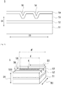
- Fig. 2 is a schematic side view of one end face of an optical element.
- Fig. 3 is a schematic perspective view of an optical element, showing that a periodic structure of grooves is provided on a main surface of an optical waveguide layer. Illustration of top clad layer of the optical element is omitted in Fig. 3 .
- Fig. 4 is a partially expanded view of the periodic structure of groove shown in Fig. 3 , schematically illustrating pitch A, depth D of groove, and angle ⁇ between bottom and side surfaces of groove.
- Fig. 1 is a schematic perspective view of a laser assembly, showing a state where a semiconductor laser device and an optical element are mounted onto a silicon substrate.
- Fig. 1 does not precisely scale the thicknesses of the silicon substrate and each element
- Fig. 5 is a process view of producing an optical element, showing that a bottom clad layer is formed onto a base substrate.
- Fig.6 is a process view of producing an optical element, showing that an optical waveguide layer is formed onto the base layer via the bottom clad layer.
- Fig. 7 is a process view of producing an optical element, showing that a first mask layer is formed onto the base layer via the bottom clad layer and the optical waveguide layer.
- Fig. 8 is a process view of producing an optical element, showing that a second mask layer made of plastic material is formed onto the base layer via the bottom clad layer, the optical waveguide layer, and the first mask layer.
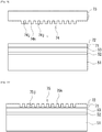
- FIG. 9 is a process view of producing an optical element, showing a state directly before the second mask layer is pressed by a mold having a pressing surface provided with a periodic structure of walls where walls extending in a first direction are arranged at constant pitch in a second direction orthogonal to a first direction.
- Fig. 10 is a process view of producing an optical element, showing a state after the second mask layer is pressed by the mold.
- Fig. 11 is a process view of producing an optical element, showing a state where arrangement of second openings are formed in the first mask layer through dry etching via first openings at the second mask layer.
- Fig. 12 is a process view of producing an optical element, showing a state a periodic structure of grooves is formed in the optical waveguide layer through dry etching via the second openings at the first mask layer.
- Fig. 13 is a process view of producing an optical element, showing a state where the first mask layer is removed.
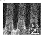
- Fig. 14 is a cross-sectional SEM image of the optical waveguide layer of the optical element according to a working example 1.
- Fig. 15 is a cross-sectional SEM image of the optical waveguide layer of the optical element according to a comparative example 1.
- Fig. 1 illustrates a laser assembly 9 which is one non-limiting application of an optical element 5 of the present disclosure.
- the laser assembly 9 has a mounting board 1 such as made of silicon (Si), a semiconductor laser device 2 mounted onto the mounting board 1, and an optical element 5 mounted onto the mounting board 1.
- the optical element 5 includes an optical waveguide layer provided with a periodic structure of grooves.
- the periodic structure of the optical waveguide layer is used as a diffraction grating for returning, to the semiconductor laser device 2, an output light from the semiconductor laser device 2, thus facilitating stability of output light wavelength of the semiconductor laser device 2.
- Types of the semiconductor laser device 2 would be various.
- Fabry-Perot laser device is used.
- the semiconductor laser device 2 has an anti-reflection coating (AR coating) on its output end face, and does not oscillate by itself.
- a single resonator may be configured by such types of semiconductor laser device 2 and diffraction grating, thus stabilities of output-wavelength and output-power are enhanced.
- a case is envisioned where a semiconductor laser device is used where a diffraction grating is not embedded in the laser element. Combination of such semiconductor laser device and an optical element of the present disclosure would allow a diffraction grating not to be embedded into the semiconductor laser device, and a stable single-wavelength light source can be produced with lesser monetary cost.
- a case is envisioned where a semiconductor laser device is used which emits a laser light with a plurality of peak wavelengths. Combination of such semiconductor laser device and an optical element of the present disclosure would allow a longitudinal mode of laser oscillation to be shifted to a single-mode, enhancing stability and selectivity of peak wavelength.
- optical elements 5 there is no limitation on the number of optical elements 5 to be associated with one semiconductor laser device 2. That is, two or more optical elements 5 may be optically coupled with one semiconductor laser device 2. The plural optical elements 5 optically coupled with the common semiconductor laser device 2 may have the same or different configurations.
- the laser element 2 is an array of laser elements where each laser element 2 has a plurality of light emitting points
- one optical element 5 is used for one array of laser elements or a plurality of optical elements 5 is used for the plurality of light emitting points.
- a plurality of diffraction grating 6 may be formed in the optical element 5 associated with one semiconductor laser device 2. That is, two or more diffraction gratings 6 may be optically coupled with one semiconductor laser device 2.
- the plurality of diffraction gratings 6 optically coupled with the common semiconductor laser device 2 may have the same or different configurations in pitch, groove-depth, and the like.
- the laser element 2 is an array of laser elements with a plurality of light emitting points
- one optical element 5 is used corresponding to a plurality of laser elements, and a plurality of diffraction gratings 6 may be optically coupled thereto respectively in this optical element 5.
- the semiconductor laser device 2 is a solid light source capable of emitting a laser light based on a current flowing between a pair of electrodes.
- the semiconductor laser device 2 has an active layer, top and bottom clad layers arranged to sandwich the active layer, a first electrode electrically coupled, e.g. in ohmic-contact with the top clad layer, and a second electrode electrically coupled with the bottom clad layer.
- the semiconductor laser device 2 has a light outputting end face 21 and a light reflecting end face 22.
- a laser resonator in the semiconductor laser device 2 is defined in the active layer of the semiconductor laser device 2 between the light outputting end face 21 and the light reflecting end face 22. In some cases, a high-reflection layer is formed onto the light reflecting end face 22, and a low-reflection layer is formed onto the light outputting end face 21.
- Wavelength of laser light emitted from the semiconductor laser device 2 would be various, but may be in an infrared band or may belong to a near-infrared ray.
- the wavelength of laser light is in a range of 750nm to 1500nm, a range of 750nm to 1000nm, a range of 750nm to 900nm.
- the wavelength of laser light is 800nm.
- oscillation wavelength of the semiconductor laser device 2 changes due to temperature dependency of bandgap of semiconductor material of the semiconductor laser device 2.
- the optical element 5 of the present disclosure is particularly advantageous for combination with such semiconductor laser device 2, not necessarily limited to this through.
- Fig. 1 schematically illustrates the active layer 25 of the semiconductor laser device 2 just for a reference.
- the active layer 25 of the semiconductor laser device 2 and the optical waveguide layer of the optical element 5 are directly bonded (butt-joint).
- an end face of the optical element 5 facing the light outputting end face 21 of the semiconductor laser device 2 is coated with an AR-coating layer (Anti-Reflection coating layer).
- AR-coating layers are formed onto the light outputting end face 21 of the semiconductor laser device 2 and the end face of the optical element 5 facing thereto so that a resonator of the semiconductor laser device 2 is extended to the optical element 5.
- the non-limiting exemplary optical element 5 shown in Fig. 2 has a base substrate 51, a bottom clad layer 52 stacked onto the base substrate 51, an optical waveguide layer 53 stacked onto the base substrate 51 via the bottom clad layer 52, and a top clad layer 54 stacked onto the base substrate 51 via the bottom clad layer 52 and the optical waveguide layer 53.
- the base substrate 51 may be a silicon substrate for example, but not necessarily limited to this and other various types of substrates can be used.
- the base substrate may be made of lithium niobate, lithium tantalate, A1N, SiC, ZnO, glass such as quartz glass, synthetic quartz and crystal, for example. In cases of glass such as quarts glass, synthetic quartz, crystal and silicon, they have better processing property.
- the bottom clad layer 52 is silicon dioxide (SiO 2 ) for example, but not necessarily limited to this. Various material with a lower refractive index than that of the optical waveguide layer 53 may be used.
- the top clad layer 54 is silicon dioxide (SiO 2 ) for example, but not necessarily limited to this. Various material with a lower refractive index than that of the optical waveguide layer 53 may be used. Other than the silicon dioxide, tantalum oxide and zinc oxide can be named as examples of material for cladding layer. Dopant may be added to the cladding layer so as to regulate the refractive index of cladding layer. For example, P, B, Al and Ga can be indicated as a dopant.
- the optical waveguide layer 53 consists of material selected from a group consisting of Ta 2 O 5 , Al 2 O 3 , LiNbO 3 , LiTaO 3 , AlN, GaN, SiC, and Yttrium aluminum garnet (YAG).
- Refractive index of the optical waveguide layer 53 is equal to or greater than 1.7, preferably equal to or greater than 2.0, in some cases.
- ⁇ ⁇ /(2n ⁇ p) is satisfied, where A indicates a pitch of arranged groove, ⁇ indicates a wavelength of laser light, n indicates a refractive index, and p indicates a diffraction order.
- the optical waveguide layer 53 has a thickness equal to or greater than 1.5 ⁇ m.
- the maximum layer-thickness of the optical waveguide layer 53 is 5 ⁇ m in some cases.
- the optical waveguide layer 53 may be doped with one or more metal elements selected from a group consisting of magnesium (Mg), zinc (Zn), scandium (Sc) and indium (In), thus the endurance against optical damage would be enhanced.
- metal elements selected from a group consisting of magnesium (Mg), zinc (Zn), scandium (Sc) and indium (In), thus the endurance against optical damage would be enhanced.
- the bottom clad layer 52, the optical waveguide layer 53 and the top clad layer 54 may be formed.
- Physical vapor deposition (PVD) or chemical vapor deposition (CVD) can be used. In most cases, sputtering is employed.
- the optical waveguide layer 53 can be formed by thinning a base.
- the bottom clad layer 52 can be formed, through thin-film forming technology, onto one side of the thinned optical waveguide layer, and this can be bonded to the base substrate 51.
- the top clad layer 54 can be formed onto the opposite side of the thinned optical waveguide layer through thin-film forming technology.
- bonding via plastic material or low-melting glass or direct bonding at room temperature can be used as a method for bonding the bottom clad layer 52 to the base substrate 51.
- the optical waveguide layer 53 has a periodic structure 6 of grooves 61.
- the main surface 535 of the optical waveguide layer 53 is provide with the periodic structure 6 configured from an arrangement of grooves 61.
- the main surface indicates a flat surface that is orthogonal to a stacking direction D1 of respective layers in the optical element 5.
- the grooves 61 are arranged at a pitch A along the groove-arrangement direction D2.
- Each groove 61 has a depth D along the stacking direction D1.
- Each groove 61 extends in a lateral direction D3 that is orthogonal to the stacking direction D1 and the groove-arrangement direction D2.
- Each groove 61 is defined by a pair of side surfaces 611, 613 facing one another in parallel substantially, and a bottom surface 612 that is arranged between the paired side surfaces 611, 613.
- the first side surface 611 is positioned closer to a light-input side of the optical element 5, in other words, positioned closer to the semiconductor laser device 2.
- the second side surface 613 is positioned closer to a light-output side of the optical element 5, in other words, positioned farther from the semiconductor laser device 2.
- the bottom surface 612 is substantially orthogonal to the stacking direction D1.
- the respective side surfaces 611, 613 are substantially orthogonal to the groove-arrangement direction D2. Note that, the side surfaces 611, 613 and the bottom surface 612 extend in the lateral direction D3. Angle between the first side surface 611 and the bottom surface 612 and angle between the second side surface 613 and the bottom surface 612 are illustrated.
- Walls 62 are formed between adjacent grooves 61 in the groove-arrangement direction D2.
- the wall 61 has a height that is equal to or close to the depth of groove 61.
- the wall 62 extends in the lateral direction D3 and is substantially orthogonal to the groove-arrangement direction D2.
- the pitch A is equal to an interval of arranged grooves in the groove-arrangement direction D2.
- the pitch A is equal to an interspace between the first side surface 611 of a first groove and the first side surface 611 of a second groove that is arranged adjacent to the first groove in the groove-arrangement direction D2, and/or an interspace between the second side surface 613 of a first groove and the second side surface 613 of a second groove that is arranged adjacent to the first groove in the groove-arrangement direction D2.
- the periodic structure 6 is used as a diffraction grating, and the pitch ⁇ of the arranged grooves in the periodic structure 6 is determined in accordance with a wavelength of laser light to be diffracted.
- the refractive index of the optical waveguide layer 53 is equal to or greater than 1.7, preferably equal to or greater than 2.0 in some cases.
- the narrowed pitch arrangement of grooves in the groove-arrangement direction D2 would ensure sufficient number of grooves within a shorter distance.
- the pitch ⁇ of the arranged grooves of the periodic structure 6 is equal to or greater than 150nm and/or equal to or less than 480nm. In some cases, the pitch ⁇ of the arranged grooves of the periodic structure 6 is equal to or greater than 150nm and equal to or less than 470nm, or equal to or greater than 167nm and equal to or less than 435, or equal to or greater than 175nm and equal to or less than 380.
- the pitch A may be equal to or greater than 150nm, 160nm, 170nm, 180nm, 190nm, 200nm, 210nm, 220nm, 230nm, 240nm, 250nm, 260nm, 270nm, 280nm, 290nm, 300nm, 310nm, 320nm, 330nm, 340nm, 350nm, 400nm or 450nm.
- the pitch A may be equal to or less than 470nm, 460nm, 450nm, 400nm, 350nm, 300nm, 250nm or 200nm.
- pitches are clearly supported by the present specification.
- various combinations would be understandable such as 150nm to 480nm, 150nm to 470nm, 160nm to 460nm, 180nm to 250nm and the like. All combinations of the lowest and highest values of the pitch are not listed here, but are substantially disclosed herein.
- the pitch A is 185nm ⁇ 0.5nm, or 239nm ⁇ 0.5nm.
- Pitch tolerance indicates a difference between a target constant value of pitch and a measurement of pitch.
- an averaged pitch tolerance that is an average of pitch tolerances is equal to or less than ⁇ 0. 5nm.
- the optical waveguide layer 53 consisting of a material selected from a group consisting of Ta 2 O 5 , Al 2 O 3 , LiNbO 3 , LiTaO 3 , AlN, GaN, SiC, and Yttrium aluminum garnet (YAG) has a layer-thickness that is equal to or greater than 1.5 ⁇ m. Furthermore, D/0.5 ⁇ 2.5 is satisfied where D indicates a depth of groove of periodic structure, A indicates pitch, and the unit of D and the unit of A are the same.
- the optical waveguide layer 53 has a thickness of 1.5 ⁇ m or more, and a periodic structure of grooves with an aspect ratio of 2.5 or more and/or a depth of 200nm or more is formed in the optical waveguide layer 53.
- Increase of the layer-thickness of the optical waveguide layer 53 allows aspect ratio and/or depth of groove 61 to be greater and allows the optical characteristics, e.g. diffraction efficiency, obtained from the given number of grooves 61 to be enhanced so that the number of grooves 61 can be reduced and the optical element can be downsized.
- the aspect ratio is equal to or greater than 3, 3.5, 4, 5, or 5.5.
- similar result may be obtained by setting the depth of groove at 200nm even the aspect ratio is 2.5 or less.
- the aspect ratio will also be increased.
- a deeper groove in the optical waveguide layer 53 consisting of a material selected from a group consisting of Ta 2 O 5 , Al 2 O 3 , LiNbO 3 , LiTaO 3 , AlN, GaN, SiC, and Yttrium aluminum garnet (YAG), and thus there may be an upper limit for the aspect ratio. In some embodiments, 2.5 ⁇ D/0.5 ⁇ 6 is satisfied.
- the optical waveguide layer 53 is made of a material selected from a group consisting of Ta 2 O 5 , Al 2 O 3 , LiNbO 3 , LiTaO 3 , AlN, GaN, SiC, and Yttrium aluminum garnet (YAG), it is first of all not easy to form a groove 61 in the optical waveguide layer 53 by dry etching, e.g. Reactive Ion Etching (RIE), and particularly to dig a deeper groove.
- RIE Reactive Ion Etching
- the grooves are arranged at a narrow pitch, deeper grooves would be more difficult to be dug. If the groove is further dug, the angle between the side surface and the bottom surface which defines the groove would be less than 90° e.g. 80° or 75°.
- V-shaped groove poses an upper limit to the aspect ratio or the maximum depth of groove, rectangular groove would be preferable in terms of diffraction efficiency.
- the depth of groove in the periodic structure 6 is equal to or greater than 200nm and/or is equal to or less than 600nm. In some cases, the depth D of the groove in the periodic structure 6 is equal to or greater than 250nm or 300nm. In some cases, the depth D of the groove in the periodic structure 6 is equal to or less than 550nm or 500nm.
- the side surfaces 611, 613 of the groove 61 are substantially vertical or slanted at angle nearby 90° relative to the bottom surface 612.
- the angle between the side surfaces 611, 613 and the bottom surface 612 satisfies ⁇ 80°, or ⁇ 82°, or ⁇ 84°, or ⁇ 86°, or ⁇ 88°. In such a case, the diffraction efficiency obtained from given number of grooves is enhanced and, as a result, reduction of number of grooves and downsizing of optical element would be facilitated.
- L ⁇ 100 ⁇ m is satisfied where L indicates an effective length of the periodic structure. In some cases, 4.5 ⁇ m ⁇ L ⁇ 70.5 ⁇ m is satisfied where L indicates an effective length of the periodic structure. In some cases, 5.01 ⁇ m ⁇ L ⁇ 65.25 ⁇ m is satisfied where L indicates an effective length of the periodic structure. In some cases, 5.25 ⁇ m ⁇ L ⁇ 57 ⁇ m is satisfied where L indicates an effective length of the periodic structure.
- Effective length L of periodic structure 6 is a length of groove arranged portion along the groove-arrangement direction D2. If the effective length L be shorter, the length K of the optical element 5 along the groove-arrangement direction D2 can be shorter. Note that, in a case where the periodic structure 6 is divided into two portions by a non-groove-formed portion, the effective length L of the periodic structure 6 is equal to the total length of the divided respective groove-formed portions and does not include the length of the non-groove-formed portion. The effective length L of the periodic structure 6 is less than the length K of the optical element 5 along the groove-arrangement direction D2. In another example, the effective length L of the periodic structure 6 is equal to the length K of the optical element 5 along the groove-arrangement direction D2. In a specific case schematically shown in Fig. 1 , the optical element 5 is smaller than the semiconductor laser device 2 in the groove-arrangement direction D2.
- the number of grooves is equal to or less than 200. Smaller number of grooves indicates shorter effective length L of periodic structure 6, allowing the optical element 5 to be downsized. In some cases, the number of grooves is 30 to 150.
- a pair of side grooves 56 is formed which extend in the groove-arrangement direction D2 to sandwich the periodic structure 6, facilitating light confinement in the lateral direction D3 by the optical waveguide layer 53, not necessarily limited to this through. Due to this pair of side grooves 56, a portion of the optical waveguide layer 53 provided with the periodic structure 6 extending in the groove-arrangement direction D2 is shaped like a ridge. In some cases, portions of the optical waveguide layer 53 adjacent in the lateral direction D3 to the ridge portion of the optical waveguide layer 53 are removed.
- a bottom clad layer 52 is formed on to a base substrate 51 through sputtering or the like (See Fig. 5 ).
- an optical waveguide layer 53 is formed onto the bottom clad layer 52 through sputtering or the like (See Fig. 6 ).
- a first mask layer 71 is formed onto the optical waveguide layer 53 through sputtering or the like (See Fig. 7 ).
- a second mask layer 72 made of plastic material is formed onto the first mask layer 71 based on a coating method such as a spin coating or the like (See Fig. 8 ).
- a mold 73 is prepared (See Fig. 9 ) and, based on pressing the mold 73 to the second mask layer 72 and irradiating of energy rays, an array of first openings 75j is formed in the second mask layer 72 (See Fig. 10 ). If necessary, a release layer is formed to the pressing surface of the mold 73 so that separation of the mold 73 off the second mask layer 72 is facilitated. In some cases, a film portion of the second mask layer remains at the bottom of the first opening, and the first opening does not completely penetrate through the second mask layer. The remaining film may have a thickness of 5nm to 100nm, for example.
- the pressing surface of the mold 73 shown in Fig. 9 is provided with a first periodic structure 74 which will finally be transferred to the optical waveguide layer 53.
- a first periodic structure 74 elongated walls 74k in a first direction are arranged at a constant pitch in the second direction that is orthogonal to the first direction.
- Each groove 74j is formed between adjacent walls 74k.
- the first direction matches the above-described lateral direction D3, and the second direction matches the above-described groove-arrangement direction D2.
- the wall 74k of the mold 73 pushes the plastic material of the second mask layer 72 away, and the plastic material of the second mask layer 72 flows into the grooves 74j adjacent to the wall 74k.
- an energy ray is irradiated so that the plastic material of the second mask layer 72 is hardened.
- the energy ray is an ultraviolet ray, but not necessarily limited to this.
- the first periodic structure 74 is transferred to the second mask layer 72 to form a second periodic structure 75.
- the second mask layer 72 is provided with first openings 75j corresponding to the walls 74k of the first periodic structure 74, and provided with first walls 75k corresponding to the grooves 74j of the first periodic structure 74.
- an array of second openings 76j is formed in the first mask layer 71 by dry etching through the first openings 75j of the second mask layer 72 (See Fig. 11 ).
- a first periodic structure 74 is transferred to the first mask layer 71 to form a third periodic structure 76.
- a second opening 76j is formed directly below the groove 75j between the walls 75k of the second periodic structure 75, and a second wall 76k is formed directly below the wall 75k of the second periodic structure 75.
- the second mask layer 72 is removed simultaneously with or after the dry etching.
- the dry etching is a reactive ion etching (RIE), as an example.
- an array of grooves 61 is formed in the optical waveguide layer 53 by dry etching through the second openings 76j of the first mask layer 71 (See Fig. 12 ).
- a first periodic structure 74 is transferred to the optical waveguide layer 53 to form the above-described periodic structure 6.
- a groove 61 is formed directly below the groove 76j between the walls 76k of the third periodic structure 76, and a wall 62 is formed directly below the wall 76k of the third periodic structure 76.
- the first mask layer 71 is removed simultaneously with or after the dry etching (See Fig. 13 ).
- the dry etching is a reactive ion etching (RIE) for example.
- side grooves 56 are formed in the optical waveguide layer 53, and a top clad layer 54 is formed onto the optical waveguide layer 53 by sputtering or the like.
- a third mask layer made of Ti or the like is formed except for a region where the side grooves 56 are to be formed, and the side grooves 56 are formed by Reactive Ion Etching through openings of the third mask layer.
- the top clad layer 54 is formed, the grooves 61 in the optical waveguide layer 53 and the side grooves 56 are filled with material of the top clad layer 54.
- End faces of the optical element 5 are formed by dicing device.
- the end face of the optical element 5 is optically polished and an AR coating is formed.
- the AR coating may have a reflectance of 0.1 %, for example.
- a laminate body is cut by dicing device so that plural chip-shaped optical elements 5 are obtained.
- the first mask layer 71 is made of metal or metal silicide.
- the first mask layer 71 is Ti, Cr, Mo, W, Ta, Si, Ni, Al, V, Fe, Nb, Re, Co, Pd, Pt or alloy thereof.
- the first mask layer 71 is tungsten silicide, vanadium silicide, iron silicide, niobium silicide, molybdenum silicide, rhenium silicide, chromium silicide, cobalt silicide, nickel silicide, palladium silicide, or platinum silicide.
- the first mask layer 71 is typically a single layer, but not necessarily limited to this.
- the second mask layer 72 is a plastic material commercially available which is usable in a nanoimprinting method (UV-curable nanoimprint resin produced by Daicel Chemical Industries, Toyo Gosei and etc.). Viscosity of plastic material of the second mask layer 72, temperature of mold at the time of transfer of periodic structure and the like would be preferably determined by a skilled person in the art.
- a halogen-based first etching gas is used during the dry etching of the first mask layer 71 through the first openings 75j of the second mask layer 72.
- a halogen-based second etching gas is used during the dry etching of the optical waveguide layer 53 through the second openings 76j of the first mask layer 71.
- the first etching gas and the second etching gas are the same in some cases, and they are different in other cases.
- the first etching gas is chlorine-based
- the second etching gas is fluorine-based.
- the first etching gas is fluorine-based
- the second etching gas is chlorine-based.
- the optical waveguide layer 53 is made of Ta 2 O 5 and the first mask layer 71 is an Al film
- a groove 61 with 2.5 or more aspect ratio is formed in the optical waveguide layer 53 having 1.5 ⁇ m or more layer thickness.
- the first etching gas is chlorine-based
- the second etching gas is fluorine-based.
- the chlorine-based etching gas is BCl 3 , for example.
- the fluorine-based etching gas is CHF 3 , for example.
- the Al film is etched by the first etching gas, causing a by-product of AlCl 3 .
- the optical waveguide layer 53 is etched by the second etching gas, causing a by-product of TaFs. In some cases, the by-product may remain in the groove of the optical element 5.
- the optical waveguide layer 53 is made of Al 2 O 3 and the first mask layer 71 is a W-film, a groove 61 with 200nm or more depth is formed in the optical waveguide layer 53 with 1.5 ⁇ m or more layer thickness.
- the first etching gas is fluorine-based
- the second etching gas is chlorine-based.
- the chlorine-based etching gas is BCl 3 , for example.
- the fluorine-based etching gas is CHF 3 , for example.
- the W-film is etched by the first etching gas, causing a by-product of WF 6 .
- the optical waveguide layer 53 is etched by the second etching gas, causing a by-product of AlCl 3 .
- the optical waveguide layer 53 is made of LiTaO 3 and the first mask layer 71 is A1 film
- a groove 61 with 2.5 or more aspect ratio is formed in the optical waveguide layer 53 with 1.5 ⁇ m or more layer thickness.
- the first etching gas is chlorine-based
- the second etching gas is fluorine-based.
- the chlorine-based etching gas is BCl 3 , for example.
- the fluorine-based etching gas is CHF 3 , for example.
- the A1 film is etched by the first etching gas, causing a by-product of AlCl 3 .
- the optical waveguide layer 53 is etched by the second etching gas, causing a by-product of TaFs. In some cases, the by-product may remain in the groove of the optical element 5.
- the optical waveguide layer 53 is made of LiNbO 3 and the first mask layer 71 is a W-film, a groove 61 with 200nm or more depth is formed in the optical waveguide layer 53 with 1.5 ⁇ m or more layer thickness.
- the first etching gas is fluorine-based
- the second etching gas is chlorine-based.
- the chlorine-based etching gas is BCl 3 , for example.
- the fluorine-based etching gas is CHF 3 , for example.
- the W film is etched by the first etching gas, causing a by-product of WF 6 .
- the optical waveguide layer 53 is etched by the second etching gas, causing a by-product of AlCl 3 .
- the optical waveguide layer 53 is made of AlN, GaN, SiC, or Yttrium aluminum garnet (YAG), material of the first mask layer 71 and types of gasses of the first and second etching gasses are appropriately determined so that grooves 61 with 2.5 or more aspect ratio and/or 200nm or more depth are formed in the optical waveguide layer 53 with 1.5 ⁇ m or more layer thickness.
- YAG Yttrium aluminum garnet
- a method of producing an optical element 5 according to an aspect of the present disclosure may include:
- the mold is configured to satisfy this condition of aspect ratio, and the dry-etching is performed to satisfy this condition of aspect ratio.
- the first mask is made of Al; chlorine-based etching gas is used for dry-etching through first openings in the second mask layer; and fluorine-based etching gas is used for dry-etching through second openings in the first mask layer.
- chlorine-based etching gas is used for dry-etching through first openings in the second mask layer; and fluorine-based etching gas is used for dry-etching through second openings in the first mask layer.
- the first mask is made of W; fluorine-based etching gas is used for dry-etching through first openings in the second mask layer; and chlorine-based etching gas is used for dry-etching through second openings in the first mask layer.
- fluorine-based etching gas is used for dry-etching through first openings in the second mask layer; and chlorine-based etching gas is used for dry-etching through second openings in the first mask layer.
- the average pitch tolerance in the periodic structure thereof is preferably within ⁇ 0.5nm.
- An average pitch tolerance should be calculated by the any one of the following methods.
- a DUV light diffraction pitch calibration may be used which can realize calibration with uncertainty of 0.04nm.
- Determined is a difference between a measurement of pitch A and a value calculated by dividing the effective length of periodic structure of optical element by the number of grooves, so that a value of tolerance is determined. Average of this tolerance can be calculated to determine an average pitch tolerance.
- a bottom clad layer made of SiO 2 was formed, by sputtering, onto a Si base substrate to have 1.0 ⁇ m thickness.
- an optical waveguide layer made of Ta 2 O 5 was formed, by spattering, onto the top surface of the bottom clad layer to have 2.0 ⁇ m thickness.
- a first mask layer made of A1 was formed, by sputtering, onto the top surface of the optical waveguide layer to have 50nm thickness.
- the second mask layer was coated onto the first mask layer to have 80nm thickness.
- the second mask layer was pressed by a mold, and plastic material of the second mask layer was hardened by irradiation of ultraviolet ray. Then the mold was removed off and an array of openings was formed in the second mask layer.
- the first mask layer was dry-etched through openings of the second mask layer by chlorine-based gas (BCl 3 ) such that openings were formed that reach the optical waveguide layer.
- BCl 3 chlorine-based gas
- the second mask layer was removed.
- the optical waveguide layer was dry-etched with fluorine-based gas (CHF 3 ) for a predetermined time window through openings in the first mask layer, thus grooves with 350nm depth were formed in the optical waveguide layer 53.
- the pitch of the arranged grooves A was 185nm.
- the angle between the side surface and the bottom surface of the groove was about 90°. This was followed by removal of the first mask layer.
- Fig. 14 shows a SEM image of one sample according to this working example (Magnification 100,000x). The aspect ratio was about 3.8. In the working example 1, upwardly opening rectangular grooves were obtained.
- Time window for etching the optical waveguide layer through openings in the first mask layer was reduced than the corresponding time window in the working example 1, and it was confirmed that the resulting aspect ratio was equal to 2.5 and the angle between the side surface and the bottom surface of the groove was substantially 90°.
- Time window for etching the optical waveguide layer through openings of the first mask layer was increased than the corresponding time window in the working example 1, and it was confirmed that the resulting aspect ratio was equal to 5.7 and the angle between the side surface and the bottom surface of the groove was substantially 90°.
- the working example 2 differs from the working example 1 in the followings: the pitch of groove ⁇ to be formed in the optical waveguide layer 53 was 239nm; Al 2 O 3 was used for the optical waveguide layer; W was used for the first mask layer; fluorine-based etching gas (CHF 3 ) was used as a gas for etching a first mask layer through openings in the second mask layer; and chlorine-based etching gas (BCl 3 ) was used as a gas for etching an optical waveguide layer through openings in the first mask layer. Similar to the working example 1, the layer thickness of the optical waveguide layer was 2.0 ⁇ m.
- the pitch of groove A in the optical waveguide layer was 239nm, and the depth of groove was 300nm, and the angle between the side surface and the bottom surface of the groove was 80°.
- the aspect ratio was about 2.5.
- upwardly opening rectangular grooves were obtained which is inferior but equivalent to that of the working example 1.
- produced and evaluated for their optical characteristics were some samples where the effective length of periodic structure of optical waveguide layer, in other words, the number of grooves 61 were varied.
- the periodic structure of optical waveguide layer is required to have the effective length of roughly 55 ⁇ m.
- a bottom clad layer made of SiO 2 was formed, by sputtering, onto a Si base substrate to have 10 ⁇ m thickness.
- an optical waveguide layer made of LiTaO 3 was formed, by spattering, onto the top surface of the bottom clad layer to have 2.0 ⁇ m thickness.
- a first mask layer made of A1 was formed, by sputtering, onto the top surface of the optical waveguide layer to have 50nm thickness.
- the second mask layer was coated onto the first mask layer to have 80nm thickness.
- the second mask layer was pressed by a mold, and plastic material of the second mask layer was hardened by irradiation of ultraviolet ray. Then, the mold was removed off and an array of openings was formed in the second mask layer.
- the first mask layer was dry-etched through openings of the second mask layer by chlorine-based gas (BCl 3 ) such that openings were formed that reach the optical waveguide layer.
- BCl 3 chlorine-based gas
- the second mask layer was removed.
- the optical waveguide layer was dry-etched with fluorine-based gas (CHF 3 ) for a predetermined time window through openings in the first mask layer, thus grooves having depth of 290nm were formed in the optical waveguide layer 53.
- the pitch A of the arranged grooves was 185nm.
- the angle between the side surface and the bottom surface of the groove was about 90°. This was followed by removal of the first mask layer.
- the aspect ratio was about 3.1. In the working example 3, upwardly opening rectangular grooves were obtained.
- a bottom clad layer made of SiO 2 was formed, by sputtering, onto a Si base substrate to have 10 ⁇ m thickness.
- an optical waveguide layer made of LiNbO 3 was formed, by spattering, onto the top surface of the bottom clad layer to have 2.0 ⁇ m thickness.
- a first mask layer made of A1 was formed, by sputtering, onto the top surface of the optical waveguide layer to have 50nm thickness.
- the second mask layer was coated onto the first mask layer to have 80nm thickness.
- the second mask layer was pressed by a mold, and plastic material of the second mask layer was hardened by irradiation of ultraviolet ray.
- the mold was removed off and an array of openings was formed in the second mask layer.
- the first mask layer was dry-etched through openings in the second mask layer by chlorine-based gas (BCl 3 ) such that openings were formed that reach the optical waveguide layer.
- the second mask layer was removed.
- the optical waveguide layer was dry-etched with fluorine-based gas (CHF 3 ) for a predetermined time window through openings in the first mask layer, thus grooves having depth of 260nm were formed in the optical waveguide layer 53.
- the pitch A of the arranged grooves was 185nm.
- the angle between the side surface and the bottom surface of the groove was about 90°. This was followed by removal of the first mask layer.
- the aspect ratio was about 2.8. In the working example 4, upwardly opening rectangular grooves were obtained.
- the comparative example 1 unlike the working example 1, Ti was used as a first mask layer, and fluorine-based gas (CHF 3 ) was used as a gas for etching the first mask layer through the openings in the second mask layer.
- a thickness of the optical waveguide layer was 2.0 ⁇ m, and this is the same as in the working example 1.
- fluorine-based gas (CHF 3 ) was used as a gas for etching the optical waveguide layer through the openings of the first mask layer.
- the pitch A of the arranged grooves in the optical waveguide layer was 185nm; the depth of groove was 150nm; and the angle between the side surface and the bottom surface of the groove was 75°.
- the aspect ratio was about 1.6.
- FIG. 15 A SEM image of one sample according to this comparative example is shown in Fig. 15 (Magnification 100,000x).
- the upwardly opening rectangular grooves as in the working example 1 were not obtained, and upwardly opening V-shaped grooves were formed.
- produced and evaluated for their optical characteristics were some samples where the effective length of periodic structure of optical waveguide layer, in other words, the number of grooves 61 were varied (See Chart 3).
- the periodic structure is required to have the Effective length of about 140 ⁇ m in order to allow an optical element to have a reflectance about 40%.
- the pitch A of the arranged grooves to be formed in the optical waveguide layer 53 was 239nm.
- fluorine-based gas (CHF 3 ) was used as a gas for etching the first mask layer through openings of second mask layer
- chlorine-based gas (BCl 3 ) was used as a gas for etching the optical waveguide layer through openings of first mask layer.
- a thickness of the optical waveguide layer was 2.0 ⁇ m, and this is the same as in the working example 2.
- the depth of groove was 190nm; and the angle between the side surface and the bottom surface of the groove was 60°.
- the aspect ratio was about 1.6.
- the periodic structure is required to have the effective length of about 140 ⁇ m in order to allow an optical element to have a reflectance about 40%.
Landscapes
- Physics & Mathematics (AREA)
- Optics & Photonics (AREA)
- General Physics & Mathematics (AREA)
- Electromagnetism (AREA)
- Engineering & Computer Science (AREA)
- Microelectronics & Electronic Packaging (AREA)
- Plasma & Fusion (AREA)
- Condensed Matter Physics & Semiconductors (AREA)
- Optical Integrated Circuits (AREA)
- Electrical Discharge Machining, Electrochemical Machining, And Combined Machining (AREA)
Abstract
Description
- The present disclosure is directed to an optical element and a method of producing the same.
-
Patent literature 1 discloses, in order to etch an optical material layer with hard-processing property, providing a base layer between a resin layer and the optical material layer, forming an opening at the resin layer using a nanoimprint technique, etching the base layer through the opening at the resin layer, and etching the optical material layer through the opening at the base layer formed by the etching, so that a deeper recess is formed in the optical material layer. - [Patent literature 1] International publication No.
2016/133161 - In a case where an optical waveguide layer consists of hard-etching material, forming deep grooves in the optical waveguide layer would be, first of all, difficult. In
Patent literature 1, a periodic structure of shallow grooves is formed in a thin layer of the optical waveguide layer. However, in its working example, grooves were formed only up to 100nm in the optical material layer made of Ta2O5. Note that, para. 0041 of thePatent literature 1 describes that the optical material layer has a layer-thickness of 0.5 to 3µm, but this is directed for a wide range of metal oxides listed in para. 0039 of the same literature and is not necessarily directed for material with highly hard-etching property. - In a case where shallow grooves are formed in a thin layer of the optical waveguide layer made of hard-etching material, there would be a problem that optical characteristics obtained from a given number of grooves, e.g. diffraction efficiency would be lowered. As a result, increased number of grooves may be required for obtaining desired optical characteristics and, in turn, the size of the optical element may be larger.
- In view of the above-described non-limiting technical challenge, the present inventors have newly identified a value of realizing an optical characteristic based on a periodic structure of an optical waveguide layer of an optical element while reducing the number of grooves in the periodic structure of the optical waveguide layer.
- An optical element according to an aspect of the present disclosure may be an optical element comprising an optical waveguide layer, the optical waveguide including a periodic structure of grooves, wherein
the optical waveguide layer has a layer-thickness equal to or greater than 1.5µm and is made of material selected from a group consisting of Ta2 O5 , Al2 O3 , LiNbO3, LiTaO3, A1N, GaN, SiC, and Yttrium aluminum garnet (YAG), and wherein
where - D indicates the depth of groove; and
- Λ indicates the pitch of the arranged grooves in the periodic structure, the unit of A being identical to the unit of D.
- In the present specification, (D/0.5A) is referred to as an aspect ratio. In the optical element according to an aspect of the present disclosure, unlike the prior approach, the optical waveguide layer has a layer-thickness equal to or greater than 1.5µm, and a periodic structure of grooves with aspect ratio of 2.5 or greater and/or depth of 200nm or greater is formed in the optical waveguide layer. Increase in the layer-thickness of the optical waveguide layer allows increase in the aspect ratio and/or groove depth, so that optical characteristic, e.g. diffraction efficiency obtained by the given number of grooves would be enhanced, thereby reducing the number of grooves and downsizing the optical element.
- In a case of working example 1 of
patent literature 1, pitch A (which is equal to an interval of arranged grooves) is 200nm, and a depth D of groove is 100nm. In this case, D/0.5A=1 is satisfied. - Layer-thickness of various layers such as the optical waveguide layer presented in the present specification would be determined based on observation of cross-section of layer using a scanning electron microscope. In particular, for measuring a thickness of a particular layer of a given product, one should basically use a scanning electron microscope FE-SEM (model JSM-7401F) produced by JEOL. If it is impossible by all means to commercially obtain this scanning electron microscope, then use of equivalent other scanning electron microscopes would be allowed.
- In some embodiments, the pitch A of the arranged grooves in the periodic structure is equal to or greater than 150nm.
- In some embodiments, the pitch Λ of the arranged grooves in the periodic structure is equal to or less than 480nm.
- In some embodiments, the pitch Λ of the arranged grooves in the periodic structure is in the range from 150nm to 470nm.
- In some embodiments, the pitch A of the arranged grooves in the periodic structure is in the range from 167nm to 435nm.
- In some embodiments, the pitch Λ of the arranged grooves in the periodic structure is in the range from 175nm to 380nm.
- In some embodiments, the depth D of the groove in the periodic structure is equal to or greater than 200nm.
- In some embodiments, the depth D of the groove in the periodic structure is equal to or greater than 250nm.
- In some embodiments, the depth D of the groove in the periodic structure is equal to or greater than 300nm.
- In some embodiments, the depth D of the groove in the periodic structure is equal to or less than 600nm.
- In some embodiments, the depth D of the groove in the periodic structure is equal to or less than 550nm.
- In some embodiments, the depth D of the groove in the periodic structure is equal to or less than 500nm.
- In some embodiments, L≦ 100µm is satisfied where L indicates an effective length of the periodic structure. Depending to embodiments, the effective length of the periodic structure satisfies: L≦ 90µm, L≦ 80µm, L≦ 70µm, L≦ 60µm, L≦ 50µm, L ≦ 40µm, L≦ 30µm, L≦ 20µm, L≦ 15µm, or L≦ 10µm.
- In some embodiments, 4.5µm≦ L ≦ 70.5µm is satisfied where L indicates an effective length of the periodic structure.
- In some embodiments, 5.01µm ≦ 65.25µm is satisfied where L indicates an effective length of the periodic structure.
- In some embodiments, 5.25µm ≦ L ≦ 57µm is satisfied where L indicates an effective length of the periodic structure.
- The effective length of the periodic structure of grooves would be understood from a viewpoint of exertion of optical characteristic based on the periodic structure. For example, in a case where non-groove arrangement region is disposed at an intermediate region between periodic structures of grooves along the groove arrangement direction, this non-groove arrangement region is not regarded as a part of the effective length of the periodic structure of grooves. The effective length of the periodic structure of grooves may be measured excluding the size of the non-groove arrangement region.
- In some embodiments, the number of grooves in the periodic structure is equal to or less than 200.
- In some embodiments, the groove in the periodic structure is defined by a pair of side surfaces opposed substantially in parallel and a bottom surface arranged between the side surfaces.
- In some embodiments, θ≧80°, or θ≧82°, or θ≧84°, or θ≧86°, or θ≧88° is satisfied where θ indicates an angle between the bottom surface and the side surface of the groove in the periodic structure.
- In some embodiments, average pitch tolerance of the grooves in the periodic structure is within ± 0.5nm.
- In some embodiments, the optical waveguide layer comprises a ridge-shaped portion provided with the periodic structure extending along the groove arrangement direction in the periodic structure.
- A laser assembly according to another aspect of the present disclosure may be a laser assembly comprising:
- an optical element of any one or any combination of above-describes ones; and
- a laser element including an active layer optically coupled with the optical waveguide layer of the optical element.
- A method of producing an optical element according to an aspect of the present disclosure may comprises:
- forming a first mask layer onto an optical waveguide layer, the optical waveguide layer having a layer-thickness equal to or greater than 1.5µm and being made of material selected from a group consisting of Ta2O5, Al2O3, LiNbO3, LiTaO3, A1N, GaN, SiC, and Yttrium aluminum garnet (YAG);
- forming, on to the first mask layer, a second mask layer that is made of plastic material;
- forming an arrangement of first openings in the second mask layer based on pressing a mold to the second mask layer and irradiating with an energy ray, the mold including a pressing surface provided with a periodic structure of walls where walls elongated in a first direction are arranged at a constant pitch along a second direction orthogonal to the first direction;
- forming an arrangement of second openings in the first mask layer by dry-etching through the first openings in the second mask layer; and
- forming a periodic structure of grooves in the optical waveguide layer by dry-etching through the second openings in the first mask layer, wherein

where- D indicates the depth of groove in the periodic structure; and
- Λ indicates the pitch of the arranged grooves in the periodic structure, the unit of A being identical to the unit of D.
- The first opening is formed mainly by the second mask layer being pressed by the mold. Therefore, an embodiment is envisioned where a film of the second mask layer remains at the bottom of the first opening, and the first opening does not completely penetrate through the second mask layer. In some cases, such remaining film is removed through ashing process such as oxygen plasma or the like. In some cases, the dry-etching through the first openings may be performed while the film remains at the first opening.
- In some embodiments, the above-described pitches Λ and groove depths D may be employed.
- In some embodiments, the groove in the periodic structure is defined by a pair of side surfaces opposed substantially in parallel and a bottom surface arranged between the side surfaces, and wherein
θ≧80°, or θ≧82°, or θ≧84°, or θ≧86°, or θ≧88° is satisfied where θ indicates an angle between the bottom surface and the side surface of the groove. - In some embodiments, average pitch tolerance of the grooves in the periodic structure is within ± 0.5nm.
- An aspect of the present disclosure may facilitate that an optical characteristic based on the periodic structure in the optical waveguide layer of the optical element is enhanced, while reducing the number of grooves in the periodic structure of the optical waveguide layer.
-
-
Fig.1 is a schematic perspective view of a laser assembly according to an aspect of the present disclosure, showing a state where a semiconductor laser device and an optical element are mounted onto a silicon substrate.Fig. 1 does not precisely scale the thicknesses of the silicon substrate and each element. -
Fig. 2 is a schematic side view of one end face of an optical element according to an aspect of the present disclosure. -
Fig. 3 is a schematic perspective view of an optical element according to an aspect of the present disclosure, showing that a periodic structure of grooves is provided on a main surface of an optical waveguide layer. Illustration of top clad layer of the optical element is omitted inFig. 3 . -
Fig. 4 is a partially expanded view of the periodic structure of groove shown inFig. 3 , schematically illustrating pitch A, depth D of groove, and angle θ between bottom and side surfaces of groove. -
Fig. 5 is a process view of producing an optical element according to an aspect of the present disclosure, showing that a bottom clad layer is formed onto a base substrate. -
Fig.6 is a process view of producing an optical element according to an aspect of the present disclosure, showing that an optical waveguide layer is formed onto the base layer via the bottom clad layer. -
Fig. 7 is a process view of producing an optical element according to an aspect of the present disclosure, showing that a first mask layer is formed onto the base layer via the bottom clad layer and the optical waveguide layer. -
Fig. 8 is a process view of producing an optical element according to an aspect of the present disclosure, showing that a second mask layer made of plastic material is formed onto the base layer via the bottom clad layer, the optical waveguide layer, and the first mask layer. -
Fig. 9 is a process view of producing an optical element according to an aspect of the present disclosure, showing a state directly before the second mask layer is pressed by a mold having a pressing surface provided with a periodic structure of walls where walls extending in a first direction are arranged at constant pitch in a second direction orthogonal to a first direction. -
Fig. 10 is a process view of producing an optical element according to an aspect of the present disclosure, showing a state after the second mask layer is pressed by the mold. -
Fig. 11 is a process view of producing an optical element according to an aspect of the present disclosure, showing a state where arrangement of second openings are formed in the first mask layer through dry etching via first openings at the second mask layer. -
Fig. 12 is a process view of producing an optical element according to an aspect of the present disclosure, showing a state a periodic structure of grooves is formed in the optical waveguide layer through dry etching via the second openings at the first mask layer. -
Fig. 13 is a process view of producing an optical element according to an aspect of the present disclosure, showing a state where the first mask layer is removed. -
Fig. 14 is a cross-sectional SEM image of the optical waveguide layer of the optical element according to a working example 1. -
Fig. 15 is a cross-sectional SEM image of the optical waveguide layer of the optical element according to a comparative example 1. - Hereinafter, non-limiting exemplary embodiments and examples of the present invention will be described with reference to
Figs. 1 to 15 . Disclosed one or more embodiments and respective features included in the embodiments are not mutually exclusive. A skilled person would be able to combine respective embodiments and/or respective features without requiring excess descriptions, and would appreciate synergistic effects of such combinations. Overlapping descriptions among the embodiments would be basically omitted. Referenced drawings are prepared for the purpose of illustration of invention, and may possibly be simplified for the sake of convenience of illustration. -
Fig.1 is a schematic perspective view of a laser assembly, showing a state where a semiconductor laser device and an optical element are mounted onto a silicon substrate.Fig. 1 does not precisely scale the thicknesses of the silicon substrate and each element.Fig. 2 is a schematic side view of one end face of an optical element.Fig. 3 is a schematic perspective view of an optical element, showing that a periodic structure of grooves is provided on a main surface of an optical waveguide layer. Illustration of top clad layer of the optical element is omitted inFig. 3 .Fig. 4 is a partially expanded view of the periodic structure of groove shown inFig. 3 , schematically illustrating pitch A, depth D of groove, and angle θ between bottom and side surfaces of groove.Fig. 5 is a process view of producing an optical element, showing that a bottom clad layer is formed onto a base substrate.Fig.6 is a process view of producing an optical element, showing that an optical waveguide layer is formed onto the base layer via the bottom clad layer.Fig. 7 is a process view of producing an optical element, showing that a first mask layer is formed onto the base layer via the bottom clad layer and the optical waveguide layer.Fig. 8 is a process view of producing an optical element, showing that a second mask layer made of plastic material is formed onto the base layer via the bottom clad layer, the optical waveguide layer, and the first mask layer.Fig. 9 is a process view of producing an optical element, showing a state directly before the second mask layer is pressed by a mold having a pressing surface provided with a periodic structure of walls where walls extending in a first direction are arranged at constant pitch in a second direction orthogonal to a first direction.Fig. 10 is a process view of producing an optical element, showing a state after the second mask layer is pressed by the mold.Fig. 11 is a process view of producing an optical element, showing a state where arrangement of second openings are formed in the first mask layer through dry etching via first openings at the second mask layer.Fig. 12 is a process view of producing an optical element, showing a state a periodic structure of grooves is formed in the optical waveguide layer through dry etching via the second openings at the first mask layer.Fig. 13 is a process view of producing an optical element, showing a state where the first mask layer is removed.Fig. 14 is a cross-sectional SEM image of the optical waveguide layer of the optical element according to a working example 1.Fig. 15 is a cross-sectional SEM image of the optical waveguide layer of the optical element according to a comparative example 1. -
Fig. 1 illustrates alaser assembly 9 which is one non-limiting application of anoptical element 5 of the present disclosure. Thelaser assembly 9 has a mountingboard 1 such as made of silicon (Si), asemiconductor laser device 2 mounted onto the mountingboard 1, and anoptical element 5 mounted onto the mountingboard 1. As would be understood from the following descriptions, theoptical element 5 includes an optical waveguide layer provided with a periodic structure of grooves. In oneexemplary laser assembly 9, the periodic structure of the optical waveguide layer is used as a diffraction grating for returning, to thesemiconductor laser device 2, an output light from thesemiconductor laser device 2, thus facilitating stability of output light wavelength of thesemiconductor laser device 2. - Types of the
semiconductor laser device 2 would be various. In an example, Fabry-Perot laser device is used. In some cases, thesemiconductor laser device 2 has an anti-reflection coating (AR coating) on its output end face, and does not oscillate by itself. A single resonator may be configured by such types ofsemiconductor laser device 2 and diffraction grating, thus stabilities of output-wavelength and output-power are enhanced. - A case is envisioned where a semiconductor laser device is used where a diffraction grating is not embedded in the laser element. Combination of such semiconductor laser device and an optical element of the present disclosure would allow a diffraction grating not to be embedded into the semiconductor laser device, and a stable single-wavelength light source can be produced with lesser monetary cost.
- A case is envisioned where a semiconductor laser device is used which emits a laser light with a plurality of peak wavelengths. Combination of such semiconductor laser device and an optical element of the present disclosure would allow a longitudinal mode of laser oscillation to be shifted to a single-mode, enhancing stability and selectivity of peak wavelength.
- Note that there is no limitation on the number of
optical elements 5 to be associated with onesemiconductor laser device 2. That is, two or moreoptical elements 5 may be optically coupled with onesemiconductor laser device 2. The pluraloptical elements 5 optically coupled with the commonsemiconductor laser device 2 may have the same or different configurations. - Further note that, in a case where the
laser element 2 is an array of laser elements where eachlaser element 2 has a plurality of light emitting points, oneoptical element 5 is used for one array of laser elements or a plurality ofoptical elements 5 is used for the plurality of light emitting points. - A plurality of
diffraction grating 6 may be formed in theoptical element 5 associated with onesemiconductor laser device 2. That is, two ormore diffraction gratings 6 may be optically coupled with onesemiconductor laser device 2. The plurality ofdiffraction gratings 6 optically coupled with the commonsemiconductor laser device 2 may have the same or different configurations in pitch, groove-depth, and the like. - In a case where the
laser element 2 is an array of laser elements with a plurality of light emitting points, oneoptical element 5 is used corresponding to a plurality of laser elements, and a plurality ofdiffraction gratings 6 may be optically coupled thereto respectively in thisoptical element 5. - The
semiconductor laser device 2 is a solid light source capable of emitting a laser light based on a current flowing between a pair of electrodes. Thesemiconductor laser device 2 has an active layer, top and bottom clad layers arranged to sandwich the active layer, a first electrode electrically coupled, e.g. in ohmic-contact with the top clad layer, and a second electrode electrically coupled with the bottom clad layer. Thesemiconductor laser device 2 has a light outputtingend face 21 and a light reflectingend face 22. A laser resonator in thesemiconductor laser device 2 is defined in the active layer of thesemiconductor laser device 2 between the light outputtingend face 21 and the light reflectingend face 22. In some cases, a high-reflection layer is formed onto the light reflectingend face 22, and a low-reflection layer is formed onto the light outputtingend face 21. - Wavelength of laser light emitted from the
semiconductor laser device 2 would be various, but may be in an infrared band or may belong to a near-infrared ray. In some cases, the wavelength of laser light is in a range of 750nm to 1500nm, a range of 750nm to 1000nm, a range of 750nm to 900nm. In a specific case, the wavelength of laser light is 800nm. When the wavelength of laser light emitted from thesemiconductor laser device 2 is in the near-infrared band, in thesemiconductor laser device 2, oscillation wavelength of thesemiconductor laser device 2 changes due to temperature dependency of bandgap of semiconductor material of thesemiconductor laser device 2. Theoptical element 5 of the present disclosure is particularly advantageous for combination with suchsemiconductor laser device 2, not necessarily limited to this through. Note that,Fig. 1 schematically illustrates theactive layer 25 of thesemiconductor laser device 2 just for a reference. - Various known methods can be employed for optically coupling the
semiconductor laser device 2 and theoptical element 5. In some cases, theactive layer 25 of thesemiconductor laser device 2 and the optical waveguide layer of theoptical element 5 are directly bonded (butt-joint). Optionally, an end face of theoptical element 5 facing the light outputtingend face 21 of thesemiconductor laser device 2 is coated with an AR-coating layer (Anti-Reflection coating layer). An embodiment is also envisioned where AR-coating layers are formed onto the light outputtingend face 21 of thesemiconductor laser device 2 and the end face of theoptical element 5 facing thereto so that a resonator of thesemiconductor laser device 2 is extended to theoptical element 5. - The non-limiting exemplary
optical element 5 shown inFig. 2 has abase substrate 51, a bottom cladlayer 52 stacked onto thebase substrate 51, anoptical waveguide layer 53 stacked onto thebase substrate 51 via the bottom cladlayer 52, and a top cladlayer 54 stacked onto thebase substrate 51 via the bottom cladlayer 52 and theoptical waveguide layer 53. - the
base substrate 51 may be a silicon substrate for example, but not necessarily limited to this and other various types of substrates can be used. The base substrate may be made of lithium niobate, lithium tantalate, A1N, SiC, ZnO, glass such as quartz glass, synthetic quartz and crystal, for example. In cases of glass such as quarts glass, synthetic quartz, crystal and silicon, they have better processing property. - The bottom clad
layer 52 is silicon dioxide (SiO2) for example, but not necessarily limited to this. Various material with a lower refractive index than that of theoptical waveguide layer 53 may be used. The top cladlayer 54 is silicon dioxide (SiO2) for example, but not necessarily limited to this. Various material with a lower refractive index than that of theoptical waveguide layer 53 may be used. Other than the silicon dioxide, tantalum oxide and zinc oxide can be named as examples of material for cladding layer. Dopant may be added to the cladding layer so as to regulate the refractive index of cladding layer. For example, P, B, Al and Ga can be indicated as a dopant. - The
optical waveguide layer 53 consists of material selected from a group consisting of Ta2O5, Al2O3, LiNbO3, LiTaO3, AlN, GaN, SiC, and Yttrium aluminum garnet (YAG). Refractive index of theoptical waveguide layer 53 is equal to or greater than 1.7, preferably equal to or greater than 2.0, in some cases. Λ=λ/(2n∗p) is satisfied, where A indicates a pitch of arranged groove, λ indicates a wavelength of laser light, n indicates a refractive index, and p indicates a diffraction order. When theoptical waveguide layer 53 is Ta2 O5 , the refractive index n of theoptical waveguide layer 53 satisfies n=2.105. When the wavelength of laser light is 800nm and p=1, the pitch of arranged groove formed in theoptical waveguide layer 53 would be Λ= about 190nm. Theoptical waveguide layer 53 has a thickness equal to or greater than 1.5µm. The maximum layer-thickness of theoptical waveguide layer 53 is 5µm in some cases. - The
optical waveguide layer 53 may be doped with one or more metal elements selected from a group consisting of magnesium (Mg), zinc (Zn), scandium (Sc) and indium (In), thus the endurance against optical damage would be enhanced. - By using various thin-film forming technology available now or in future, the bottom clad
layer 52, theoptical waveguide layer 53 and the top cladlayer 54 may be formed. Physical vapor deposition (PVD) or chemical vapor deposition (CVD) can be used. In most cases, sputtering is employed. - The
optical waveguide layer 53 can be formed by thinning a base. In this case, the bottom cladlayer 52 can be formed, through thin-film forming technology, onto one side of the thinned optical waveguide layer, and this can be bonded to thebase substrate 51. Then, the top cladlayer 54 can be formed onto the opposite side of the thinned optical waveguide layer through thin-film forming technology. As a method for bonding the bottom cladlayer 52 to thebase substrate 51, bonding via plastic material or low-melting glass or direct bonding at room temperature can be used. - As schematically illustrated in
Figs. 3 and4 , theoptical waveguide layer 53 has aperiodic structure 6 ofgrooves 61. Themain surface 535 of theoptical waveguide layer 53 is provide with theperiodic structure 6 configured from an arrangement ofgrooves 61. The main surface indicates a flat surface that is orthogonal to a stacking direction D1 of respective layers in theoptical element 5. In theperiodic structure 6, thegrooves 61 are arranged at a pitch A along the groove-arrangement direction D2. Eachgroove 61 has a depth D along the stacking direction D1. Eachgroove 61 extends in a lateral direction D3 that is orthogonal to the stacking direction D1 and the groove-arrangement direction D2. - Each
groove 61 is defined by a pair of side surfaces 611, 613 facing one another in parallel substantially, and abottom surface 612 that is arranged between the paired side surfaces 611, 613. In onegroove 61, thefirst side surface 611 is positioned closer to a light-input side of theoptical element 5, in other words, positioned closer to thesemiconductor laser device 2. Thesecond side surface 613 is positioned closer to a light-output side of theoptical element 5, in other words, positioned farther from thesemiconductor laser device 2. Thebottom surface 612 is substantially orthogonal to the stacking direction D1. The respective side surfaces 611, 613 are substantially orthogonal to the groove-arrangement direction D2. Note that, the side surfaces 611, 613 and thebottom surface 612 extend in the lateral direction D3. Angle between thefirst side surface 611 and thebottom surface 612 and angle between thesecond side surface 613 and thebottom surface 612 are illustrated. -
Walls 62 are formed betweenadjacent grooves 61 in the groove-arrangement direction D2. Thewall 61 has a height that is equal to or close to the depth ofgroove 61. Thewall 62 extends in the lateral direction D3 and is substantially orthogonal to the groove-arrangement direction D2. - The pitch A is equal to an interval of arranged grooves in the groove-arrangement direction D2. The pitch A is equal to an interspace between the
first side surface 611 of a first groove and thefirst side surface 611 of a second groove that is arranged adjacent to the first groove in the groove-arrangement direction D2, and/or an interspace between thesecond side surface 613 of a first groove and thesecond side surface 613 of a second groove that is arranged adjacent to the first groove in the groove-arrangement direction D2. - The
periodic structure 6 is used as a diffraction grating, and the pitch Λ of the arranged grooves in theperiodic structure 6 is determined in accordance with a wavelength of laser light to be diffracted. As described above, the refractive index of theoptical waveguide layer 53 is equal to or greater than 1.7, preferably equal to or greater than 2.0 in some cases. When theoptical waveguide layer 53 is Ta2 O5, the refractive index n of theoptical waveguide layer 53 satisfies n=2.105. The narrowed pitch arrangement of grooves in the groove-arrangement direction D2 would ensure sufficient number of grooves within a shorter distance. - In some embodiments, the pitch Λ of the arranged grooves of the
periodic structure 6 is equal to or greater than 150nm and/or equal to or less than 480nm. In some cases, the pitch Λ of the arranged grooves of theperiodic structure 6 is equal to or greater than 150nm and equal to or less than 470nm, or equal to or greater than 167nm and equal to or less than 435, or equal to or greater than 175nm and equal to or less than 380. Dependent to embodiments, the pitch A may be equal to or greater than 150nm, 160nm, 170nm, 180nm, 190nm, 200nm, 210nm, 220nm, 230nm, 240nm, 250nm, 260nm, 270nm, 280nm, 290nm, 300nm, 310nm, 320nm, 330nm, 340nm, 350nm, 400nm or 450nm. Dependent to embodiments, the pitch A may be equal to or less than 470nm, 460nm, 450nm, 400nm, 350nm, 300nm, 250nm or 200nm. - Any combinations of the lowest and highest values of the above-described pitches are clearly supported by the present specification. As a numerical range of pitch A, various combinations would be understandable such as 150nm to 480nm, 150nm to 470nm, 160nm to 460nm, 180nm to 250nm and the like. All combinations of the lowest and highest values of the pitch are not listed here, but are substantially disclosed herein. In a specific embodiment, the pitch A is 185nm ± 0.5nm, or 239nm ± 0.5nm.
- The pitch of the arranged grooves in the periodic structure would suffer fluctuation from various factors, i.e. tolerance or variation is caused in the pitch. Pitch tolerance indicates a difference between a target constant value of pitch and a measurement of pitch. In some cases, an averaged pitch tolerance that is an average of pitch tolerances is equal to or less than ±0. 5nm.
- In the present embodiment, the
optical waveguide layer 53 consisting of a material selected from a group consisting of Ta2O5 , Al2O3 , LiNbO3 , LiTaO3, AlN, GaN, SiC, and Yttrium aluminum garnet (YAG) has a layer-thickness that is equal to or greater than 1.5µm. Furthermore, D/0.5Λ≧2.5 is satisfied where D indicates a depth of groove of periodic structure, A indicates pitch, and the unit of D and the unit of A are the same. - In the present embodiment, the
optical waveguide layer 53 has a thickness of 1.5µm or more, and a periodic structure of grooves with an aspect ratio of 2.5 or more and/or a depth of 200nm or more is formed in theoptical waveguide layer 53. Increase of the layer-thickness of theoptical waveguide layer 53 allows aspect ratio and/or depth ofgroove 61 to be greater and allows the optical characteristics, e.g. diffraction efficiency, obtained from the given number ofgrooves 61 to be enhanced so that the number ofgrooves 61 can be reduced and the optical element can be downsized. - Dependent to embodiments, the aspect ratio is equal to or greater than 3, 3.5, 4, 5, or 5.5. Dependent to embodiments, similar result may be obtained by setting the depth of groove at 200nm even the aspect ratio is 2.5 or less.
- Under the same pitch A, if the depth D of
groove 61 is increased, then the aspect ratio will also be increased. However, it is first of all difficult to form a deeper groove in theoptical waveguide layer 53 consisting of a material selected from a group consisting of Ta2O5 , Al2O3 , LiNbO3 , LiTaO3, AlN, GaN, SiC, and Yttrium aluminum garnet (YAG), and thus there may be an upper limit for the aspect ratio. In some embodiments, 2.5≦D/0.5Λ≦6 is satisfied. - In a case where the
optical waveguide layer 53 is made of a material selected from a group consisting of Ta2O5, Al2O3, LiNbO3, LiTaO3, AlN, GaN, SiC, and Yttrium aluminum garnet (YAG), it is first of all not easy to form agroove 61 in theoptical waveguide layer 53 by dry etching, e.g. Reactive Ion Etching (RIE), and particularly to dig a deeper groove. When the grooves are arranged at a narrow pitch, deeper grooves would be more difficult to be dug. If the groove is further dug, the angle between the side surface and the bottom surface which defines the groove would be less than 90° e.g. 80° or 75°. That is, it would not be an upwardly-opening rectangular groove in a cross-section, but would be an upwardly-opening V-shaped groove in a cross-section. As the V-shaped groove poses an upper limit to the aspect ratio or the maximum depth of groove, rectangular groove would be preferable in terms of diffraction efficiency. - In some embodiments, the depth of groove in the
periodic structure 6 is equal to or greater than 200nm and/or is equal to or less than 600nm. In some cases, the depth D of the groove in theperiodic structure 6 is equal to or greater than 250nm or 300nm. In some cases, the depth D of the groove in theperiodic structure 6 is equal to or less than 550nm or 500nm. - In some embodiments, the side surfaces 611, 613 of the
groove 61 are substantially vertical or slanted at angle nearby 90° relative to thebottom surface 612. In some cases, the angle between the side surfaces 611, 613 and thebottom surface 612 satisfies θ≧80°, or θ≧82°, or θ≧84°, or θ≧86°, or θ≧88°. In such a case, the diffraction efficiency obtained from given number of grooves is enhanced and, as a result, reduction of number of grooves and downsizing of optical element would be facilitated. - In some cases, L≦100µm is satisfied where L indicates an effective length of the periodic structure. In some cases, 4.5µm≦L≦70.5µm is satisfied where L indicates an effective length of the periodic structure. In some cases, 5.01µm≦L≦ 65.25µm is satisfied where L indicates an effective length of the periodic structure. In some cases, 5.25µm≦L≦57µm is satisfied where L indicates an effective length of the periodic structure.
- Effective length L of
periodic structure 6 is a length of groove arranged portion along the groove-arrangement direction D2. If the effective length L be shorter, the length K of theoptical element 5 along the groove-arrangement direction D2 can be shorter. Note that, in a case where theperiodic structure 6 is divided into two portions by a non-groove-formed portion, the effective length L of theperiodic structure 6 is equal to the total length of the divided respective groove-formed portions and does not include the length of the non-groove-formed portion. The effective length L of theperiodic structure 6 is less than the length K of theoptical element 5 along the groove-arrangement direction D2. In another example, the effective length L of theperiodic structure 6 is equal to the length K of theoptical element 5 along the groove-arrangement direction D2. In a specific case schematically shown inFig. 1 , theoptical element 5 is smaller than thesemiconductor laser device 2 in the groove-arrangement direction D2. - In some cases, the number of grooves is equal to or less than 200. Smaller number of grooves indicates shorter effective length L of
periodic structure 6, allowing theoptical element 5 to be downsized. In some cases, the number of grooves is 30 to 150. - A pair of
side grooves 56 is formed which extend in the groove-arrangement direction D2 to sandwich theperiodic structure 6, facilitating light confinement in the lateral direction D3 by theoptical waveguide layer 53, not necessarily limited to this through. Due to this pair ofside grooves 56, a portion of theoptical waveguide layer 53 provided with theperiodic structure 6 extending in the groove-arrangement direction D2 is shaped like a ridge. In some cases, portions of theoptical waveguide layer 53 adjacent in the lateral direction D3 to the ridge portion of theoptical waveguide layer 53 are removed. - Hereinafter, a non-limiting exemplary method of producing an
optical element 5 will be discussed with reference toFigs. 5 to 13 . Firstly, a bottom cladlayer 52 is formed on to abase substrate 51 through sputtering or the like (SeeFig. 5 ). Next, anoptical waveguide layer 53 is formed onto the bottom cladlayer 52 through sputtering or the like (SeeFig. 6 ). Afirst mask layer 71 is formed onto theoptical waveguide layer 53 through sputtering or the like (SeeFig. 7 ). Next, asecond mask layer 72 made of plastic material is formed onto thefirst mask layer 71 based on a coating method such as a spin coating or the like (SeeFig. 8 ). Next, amold 73 is prepared (SeeFig. 9 ) and, based on pressing themold 73 to thesecond mask layer 72 and irradiating of energy rays, an array offirst openings 75j is formed in the second mask layer 72 (SeeFig. 10 ). If necessary, a release layer is formed to the pressing surface of themold 73 so that separation of themold 73 off thesecond mask layer 72 is facilitated. In some cases, a film portion of the second mask layer remains at the bottom of the first opening, and the first opening does not completely penetrate through the second mask layer. The remaining film may have a thickness of 5nm to 100nm, for example. - The pressing surface of the
mold 73 shown inFig. 9 is provided with a firstperiodic structure 74 which will finally be transferred to theoptical waveguide layer 53. In the firstperiodic structure 74, elongatedwalls 74k in a first direction are arranged at a constant pitch in the second direction that is orthogonal to the first direction. Eachgroove 74j is formed betweenadjacent walls 74k. The first direction matches the above-described lateral direction D3, and the second direction matches the above-described groove-arrangement direction D2. When thesecond mask layer 72 is pressed by themold 73 under a condition where the plastic material of thesecond mask layer 72 is softened, thewall 74k of themold 73 pushes the plastic material of thesecond mask layer 72 away, and the plastic material of thesecond mask layer 72 flows into thegrooves 74j adjacent to thewall 74k. Under this state, an energy ray is irradiated so that the plastic material of thesecond mask layer 72 is hardened. The energy ray is an ultraviolet ray, but not necessarily limited to this. As such, the firstperiodic structure 74 is transferred to thesecond mask layer 72 to form a secondperiodic structure 75. Thesecond mask layer 72 is provided withfirst openings 75j corresponding to thewalls 74k of the firstperiodic structure 74, and provided withfirst walls 75k corresponding to thegrooves 74j of the firstperiodic structure 74. - Next, an array of second openings 76j is formed in the
first mask layer 71 by dry etching through thefirst openings 75j of the second mask layer 72 (SeeFig. 11 ). As such, a firstperiodic structure 74 is transferred to thefirst mask layer 71 to form a thirdperiodic structure 76. In thefirst mask layer 71, a second opening 76j is formed directly below thegroove 75j between thewalls 75k of the secondperiodic structure 75, and asecond wall 76k is formed directly below thewall 75k of the secondperiodic structure 75. Thesecond mask layer 72 is removed simultaneously with or after the dry etching. The dry etching is a reactive ion etching (RIE), as an example. - Next, an array of
grooves 61 is formed in theoptical waveguide layer 53 by dry etching through the second openings 76j of the first mask layer 71 (SeeFig. 12 ). As such, a firstperiodic structure 74 is transferred to theoptical waveguide layer 53 to form the above-describedperiodic structure 6. In theoptical waveguide layer 53, agroove 61 is formed directly below the groove 76j between thewalls 76k of the thirdperiodic structure 76, and awall 62 is formed directly below thewall 76k of the thirdperiodic structure 76. Thefirst mask layer 71 is removed simultaneously with or after the dry etching (SeeFig. 13 ). The dry etching is a reactive ion etching (RIE) for example. - After that,
side grooves 56 are formed in theoptical waveguide layer 53, and a top cladlayer 54 is formed onto theoptical waveguide layer 53 by sputtering or the like. Regarding theside grooves 56, a third mask layer made of Ti or the like is formed except for a region where theside grooves 56 are to be formed, and theside grooves 56 are formed by Reactive Ion Etching through openings of the third mask layer. After the top cladlayer 54 is formed, thegrooves 61 in theoptical waveguide layer 53 and theside grooves 56 are filled with material of the top cladlayer 54. End faces of theoptical element 5 are formed by dicing device. Next, the end face of theoptical element 5 is optically polished and an AR coating is formed. The AR coating may have a reflectance of 0.1 %, for example. In a case where pluraloptical elements 5 are produced over onebase substrate 51, a laminate body is cut by dicing device so that plural chip-shapedoptical elements 5 are obtained. - In some cases, the
first mask layer 71 is made of metal or metal silicide. For example, thefirst mask layer 71 is Ti, Cr, Mo, W, Ta, Si, Ni, Al, V, Fe, Nb, Re, Co, Pd, Pt or alloy thereof. For example, thefirst mask layer 71 is tungsten silicide, vanadium silicide, iron silicide, niobium silicide, molybdenum silicide, rhenium silicide, chromium silicide, cobalt silicide, nickel silicide, palladium silicide, or platinum silicide. Thefirst mask layer 71 is typically a single layer, but not necessarily limited to this. - The
second mask layer 72 is a plastic material commercially available which is usable in a nanoimprinting method (UV-curable nanoimprint resin produced by Daicel Chemical Industries, Toyo Gosei and etc.). Viscosity of plastic material of thesecond mask layer 72, temperature of mold at the time of transfer of periodic structure and the like would be preferably determined by a skilled person in the art. - A halogen-based first etching gas is used during the dry etching of the
first mask layer 71 through thefirst openings 75j of thesecond mask layer 72. A halogen-based second etching gas is used during the dry etching of theoptical waveguide layer 53 through the second openings 76j of thefirst mask layer 71. The first etching gas and the second etching gas are the same in some cases, and they are different in other cases. In one case, the first etching gas is chlorine-based, and the second etching gas is fluorine-based. In another case, the first etching gas is fluorine-based, and the second etching gas is chlorine-based. - It has been confirmed that, when the
optical waveguide layer 53 is made of Ta2 O5 and thefirst mask layer 71 is an Al film, agroove 61 with 2.5 or more aspect ratio is formed in theoptical waveguide layer 53 having 1.5µm or more layer thickness. The first etching gas is chlorine-based, and the second etching gas is fluorine-based. The chlorine-based etching gas is BCl3, for example. The fluorine-based etching gas is CHF3, for example. The Al film is etched by the first etching gas, causing a by-product of AlCl3. Theoptical waveguide layer 53 is etched by the second etching gas, causing a by-product of TaFs. In some cases, the by-product may remain in the groove of theoptical element 5. - It has been confirmed that, when the
optical waveguide layer 53 is made of Al2 O3 and thefirst mask layer 71 is a W-film, agroove 61 with 200nm or more depth is formed in theoptical waveguide layer 53 with 1.5µm or more layer thickness. The first etching gas is fluorine-based, and the second etching gas is chlorine-based. The chlorine-based etching gas is BCl3, for example. The fluorine-based etching gas is CHF3, for example. The W-film is etched by the first etching gas, causing a by-product of WF6. Theoptical waveguide layer 53 is etched by the second etching gas, causing a by-product of AlCl3. - It has been confirmed that, when the
optical waveguide layer 53 is made of LiTaO3 and thefirst mask layer 71 is A1 film, agroove 61 with 2.5 or more aspect ratio is formed in theoptical waveguide layer 53 with 1.5µm or more layer thickness. The first etching gas is chlorine-based, and the second etching gas is fluorine-based. The chlorine-based etching gas is BCl3, for example. The fluorine-based etching gas is CHF3, for example. The A1 film is etched by the first etching gas, causing a by-product of AlCl3. Theoptical waveguide layer 53 is etched by the second etching gas, causing a by-product of TaFs. In some cases, the by-product may remain in the groove of theoptical element 5. - It has been confirmed that, when the
optical waveguide layer 53 is made of LiNbO3 and thefirst mask layer 71 is a W-film, agroove 61 with 200nm or more depth is formed in theoptical waveguide layer 53 with 1.5µm or more layer thickness. The first etching gas is fluorine-based, and the second etching gas is chlorine-based. The chlorine-based etching gas is BCl3, for example. The fluorine-based etching gas is CHF3, for example. The W film is etched by the first etching gas, causing a by-product of WF6. Theoptical waveguide layer 53 is etched by the second etching gas, causing a by-product of AlCl3. - In cases where the
optical waveguide layer 53 is made of AlN, GaN, SiC, or Yttrium aluminum garnet (YAG), material of thefirst mask layer 71 and types of gasses of the first and second etching gasses are appropriately determined so thatgrooves 61 with 2.5 or more aspect ratio and/or 200nm or more depth are formed in theoptical waveguide layer 53 with 1.5µm or more layer thickness. - As would be understood from above descriptions, a method of producing an
optical element 5 according to an aspect of the present disclosure may include: - forming a first mask layer onto an optical waveguide layer, the optical waveguide layer having a layer-thickness equal to or greater than 1.5µm and being made of material selected from a group consisting of Ta2O5, Al2O3, LiNbO3, LiTaO3, A1N, GaN, SiC, and Yttrium aluminum garnet (YAG);
- forming, on to the first mask layer, a second mask layer that is made of plastic material;
- forming an arrangement of first openings in the second mask layer based on pressing a mold to the second mask layer and irradiating with an energy ray, the mold including a pressing surface provided with a periodic structure of walls where walls elongated in a first direction are arranged at a constant pitch along a second direction orthogonal to the first direction;
- forming an arrangement of second openings in the first mask layer by dry-etching through the first openings in the second mask layer; and
- forming a periodic structure of grooves in the optical waveguide layer by dry-etching through the second openings in the first mask layer, wherein

where- D indicates the depth of groove in the periodic structure; and
- A indicates the pitch, the unit of A being identical to the unit of D.
- In other words, the mold is configured to satisfy this condition of aspect ratio, and the dry-etching is performed to satisfy this condition of aspect ratio.
- As an exemplary set of conditions, the first mask is made of Al; chlorine-based etching gas is used for dry-etching through first openings in the second mask layer; and fluorine-based etching gas is used for dry-etching through second openings in the first mask layer. Detailed conditions are disclosed in a working example 1.
- As another set of conditions, the first mask is made of W; fluorine-based etching gas is used for dry-etching through first openings in the second mask layer; and chlorine-based etching gas is used for dry-etching through second openings in the first mask layer. Detailed conditions are disclosed in a working example 2.
- As to an optical element with a pitch A, the average pitch tolerance in the periodic structure thereof is preferably within ± 0.5nm. An average pitch tolerance should be calculated by the any one of the following methods.
- First of all, a DUV light diffraction pitch calibration may be used which can realize calibration with uncertainty of 0.04nm.
- In a working example 1 described below, when the average pitch tolerance of periodic structure was evaluated based on the DUV light diffraction pitch calibration for an optical element with groove depth 500nm and pitch 185nm, we confirmed the tolerance of accuracy was within ±0.03nm.
- Determined is a difference between a measurement of pitch A and a value calculated by dividing the effective length of periodic structure of optical element by the number of grooves, so that a value of tolerance is determined. Average of this tolerance can be calculated to determine an average pitch tolerance.
- A bottom clad layer made of SiO2 was formed, by sputtering, onto a Si base substrate to have 1.0µm thickness. Next, an optical waveguide layer made of Ta2O5 was formed, by spattering, onto the top surface of the bottom clad layer to have 2.0µm thickness. Next, a first mask layer made of A1 was formed, by sputtering, onto the top surface of the optical waveguide layer to have 50nm thickness. Next, the second mask layer was coated onto the first mask layer to have 80nm thickness. Next, the second mask layer was pressed by a mold, and plastic material of the second mask layer was hardened by irradiation of ultraviolet ray. Then the mold was removed off and an array of openings was formed in the second mask layer. Next, the first mask layer was dry-etched through openings of the second mask layer by chlorine-based gas (BCl3) such that openings were formed that reach the optical waveguide layer. At the same time of this dry-etching, the second mask layer was removed. Next, the optical waveguide layer was dry-etched with fluorine-based gas (CHF3) for a predetermined time window through openings in the first mask layer, thus grooves with 350nm depth were formed in the
optical waveguide layer 53. The pitch of the arranged grooves A was 185nm. The angle between the side surface and the bottom surface of the groove was about 90°. This was followed by removal of the first mask layer.Fig. 14 shows a SEM image of one sample according to this working example (Magnification 100,000x). The aspect ratio was about 3.8. In the working example 1, upwardly opening rectangular grooves were obtained. - Next, side grooves were formed that have a width of 2µm and a depth of 1.6µm in the optical waveguide layer, so that the
optical waveguide layer 53 was shaped like a ridge. Next, the top clad layer made of SiO2 and having a thickness of 0.5µm was formed, by sputtering. Then, the laminate body was cut into a bar-shape by a dicing device, and the both end faces formed by the cutting were optically polished. Thereafter, AR coatings with 0.1% reflectance were formed onto the respective end faces. The bar-shaped laminate body was cut so that chip-like optical elements were obtained. The optical element had a size of 1mm width and 500µm length. - In the working example 1, produced and evaluated for their optical characteristics were some samples where the effective length of periodic structure of optical waveguide layer, in other words, the number of
grooves 61 were varied. For the purpose of evaluation, a super luminescence diode (SLD), which is a wide frequency band light source, was used. An emitted light from the SLD was input to the optical element, and an output light from the optical element was analyzed by an optical spectrum analyzer. Reflection characteristics was evaluated form transparency characteristics of the optical element. For one given wavelength, here 800µm, reflectance of optical element was measured. Thechart 1 below shows the result.[Chart 1] Effective length of periodic structure of optical waveguide layer (µm) Reflectance (%) 10 31 20 73 30 91 40 97 50 99 60 100 70 100 80 100 90 100 100 100 - It is understandable that, in order to achieve roughly 40% reflectance of the optical element, roughly 13µm of the effective length of periodic structure of optical waveguide layer is sufficient. It is confirmed that the effective length of the
periodic structure 6 was greatly reduced, and the reduction in size of optical element was facilitated greatly. - Time window for etching the optical waveguide layer through openings in the first mask layer was reduced than the corresponding time window in the working example 1, and it was confirmed that the resulting aspect ratio was equal to 2.5 and the angle between the side surface and the bottom surface of the groove was substantially 90°. Time window for etching the optical waveguide layer through openings of the first mask layer was increased than the corresponding time window in the working example 1, and it was confirmed that the resulting aspect ratio was equal to 5.7 and the angle between the side surface and the bottom surface of the groove was substantially 90°.
- The working example 2 differs from the working example 1 in the followings: the pitch of groove Λ to be formed in the
optical waveguide layer 53 was 239nm; Al2O3 was used for the optical waveguide layer; W was used for the first mask layer; fluorine-based etching gas (CHF3) was used as a gas for etching a first mask layer through openings in the second mask layer; and chlorine-based etching gas (BCl3) was used as a gas for etching an optical waveguide layer through openings in the first mask layer. Similar to the working example 1, the layer thickness of the optical waveguide layer was 2.0µm. The pitch of groove A in the optical waveguide layer was 239nm, and the depth of groove was 300nm, and the angle between the side surface and the bottom surface of the groove was 80°. The aspect ratio was about 2.5. In a case of working example 2, upwardly opening rectangular grooves were obtained which is inferior but equivalent to that of the working example 1. In working example 2 either as in the working example 1, produced and evaluated for their optical characteristics were some samples where the effective length of periodic structure of optical waveguide layer, in other words, the number ofgrooves 61 were varied.[Chart 2] Effective length of periodic structure of optical waveguide layer (µm) Reflectance (%) 10 2 20 7 30 16 40 26 50 37 60 48 70 57 80 66 90 73 100 79 - In a case of working example 2, it is understandable that, in order to achieve roughly 40% reflectance of the optical element, the periodic structure of optical waveguide layer is required to have the effective length of roughly 55µm.
- In the case of working example 2, aspect ratio >2.5 and, even compared with comparative example 1, it is confirmed that effective length of periodic structure of optical waveguide layer is advantageously reduced, similar to working example 1.
- A bottom clad layer made of SiO2 was formed, by sputtering, onto a Si base substrate to have 10µm thickness. Next, an optical waveguide layer made of LiTaO3 was formed, by spattering, onto the top surface of the bottom clad layer to have 2.0µm thickness. Next, a first mask layer made of A1 was formed, by sputtering, onto the top surface of the optical waveguide layer to have 50nm thickness. Next, the second mask layer was coated onto the first mask layer to have 80nm thickness. Next, the second mask layer was pressed by a mold, and plastic material of the second mask layer was hardened by irradiation of ultraviolet ray. Then, the mold was removed off and an array of openings was formed in the second mask layer. Next, the first mask layer was dry-etched through openings of the second mask layer by chlorine-based gas (BCl3) such that openings were formed that reach the optical waveguide layer. At the same time of this dry-etching, the second mask layer was removed. Next, the optical waveguide layer was dry-etched with fluorine-based gas (CHF3) for a predetermined time window through openings in the first mask layer, thus grooves having depth of 290nm were formed in the
optical waveguide layer 53. The pitch A of the arranged grooves was 185nm. The angle between the side surface and the bottom surface of the groove was about 90°. This was followed by removal of the first mask layer. The aspect ratio was about 3.1. In the working example 3, upwardly opening rectangular grooves were obtained. - A bottom clad layer made of SiO2 was formed, by sputtering, onto a Si base substrate to have 10µm thickness. Next, an optical waveguide layer made of LiNbO3 was formed, by spattering, onto the top surface of the bottom clad layer to have 2.0µm thickness. Next, a first mask layer made of A1 was formed, by sputtering, onto the top surface of the optical waveguide layer to have 50nm thickness. Next, the second mask layer was coated onto the first mask layer to have 80nm thickness. Next, the second mask layer was pressed by a mold, and plastic material of the second mask layer was hardened by irradiation of ultraviolet ray.
- Then, the mold was removed off and an array of openings was formed in the second mask layer. Next, the first mask layer was dry-etched through openings in the second mask layer by chlorine-based gas (BCl3) such that openings were formed that reach the optical waveguide layer. At the same time of this dry-etching, the second mask layer was removed. Next, the optical waveguide layer was dry-etched with fluorine-based gas (CHF3) for a predetermined time window through openings in the first mask layer, thus grooves having depth of 260nm were formed in the
optical waveguide layer 53. The pitch A of the arranged grooves was 185nm. The angle between the side surface and the bottom surface of the groove was about 90°. This was followed by removal of the first mask layer. The aspect ratio was about 2.8. In the working example 4, upwardly opening rectangular grooves were obtained. - In the comparative example 1, unlike the working example 1, Ti was used as a first mask layer, and fluorine-based gas (CHF3) was used as a gas for etching the first mask layer through the openings in the second mask layer. A thickness of the optical waveguide layer was 2.0µm, and this is the same as in the working example 1. Similar to the working example 1, fluorine-based gas (CHF3) was used as a gas for etching the optical waveguide layer through the openings of the first mask layer. The pitch A of the arranged grooves in the optical waveguide layer was 185nm; the depth of groove was 150nm; and the angle between the side surface and the bottom surface of the groove was 75°. The aspect ratio was about 1.6. A SEM image of one sample according to this comparative example is shown in
Fig. 15 (Magnification 100,000x). In the case of comparative example 1, the upwardly opening rectangular grooves as in the working example 1 were not obtained, and upwardly opening V-shaped grooves were formed. In comparative example 1, produced and evaluated for their optical characteristics were some samples where the effective length of periodic structure of optical waveguide layer, in other words, the number ofgrooves 61 were varied (See Chart 3).[Chart 3] Effective length of periodic structure of optical waveguide layer (µm) reflectance (%) 30 3 60 10 90 20 120 32 150 44 180 56 210 65 240 74 270 80 300 85 - In the case of comparative example 1, it is understandable that the periodic structure is required to have the Effective length of about 140µm in order to allow an optical element to have a reflectance about 40%.
- In the comparative example 2, unlike the working example 2, Ti was used as a first mask layer. Similar to the working example 2, the pitch A of the arranged grooves to be formed in the
optical waveguide layer 53 was 239nm. Similar to the working example 2, fluorine-based gas (CHF3) was used as a gas for etching the first mask layer through openings of second mask layer, and chlorine-based gas (BCl3) was used as a gas for etching the optical waveguide layer through openings of first mask layer. A thickness of the optical waveguide layer was 2.0µm, and this is the same as in the working example 2. The depth of groove was 190nm; and the angle between the side surface and the bottom surface of the groove was 60°. The aspect ratio was about 1.6. In the case of comparative example 2, the upwardly opening rectangular grooves as in the working example 2 were not obtained, and upwardly opening V-shaped grooves were formed. In comparative example 2, some samples having, as variation, effective length of periodic structure of optical waveguide layer i.e. the number ofgrooves 61 were produced and evaluated for their optical characteristics as in the working example 2 (See Chart 4).[Chart 4] Effective length of periodic structure of optical waveguide layer (µm) Reflectance (%) 30 3 60 10 90 20 120 32 150 44 180 56 210 65 240 74 270 80 300 85 - In the case of comparative example 2, it is understandable that the periodic structure is required to have the effective length of about 140µm in order to allow an optical element to have a reflectance about 40%.
- Based on the above teaching, a skilled person in the art would be able to add various modifications to the respective embodiments. Reference numerals in Claims are just for reference and should not be referred for the purpose of narrowly construing the scope of claims.
-
- 51
- Base substrate
- 52
- Bottom clad layer
- 53
- Optical waveguide layer
- 54
- Top clad layer
- 56
- Side groove
Claims (25)
- An optical element comprising an optical waveguide layer, the optical waveguide including a periodic structure of grooves, wherein
the optical waveguide layer has a layer-thickness equal to or greater than 1.5µm and is made of material selected from a group consisting of Ta2O5, Al2O3, LiNbO3, LiTaO3, AlN, GaN, SiC, and Yttrium aluminum garnet (YAG), and wherein
whereD indicates the depth of groove; andΛ indicates the pitch of the arranged grooves in the periodic structure, the unit of A being identical to the unit of D. - The optical element of Claim 1, wherein the pitch A of the arranged grooves in the periodic structure is equal to or greater than 150nm.
- The optical element of Claim 1 or 2, wherein the pitch A of the arranged grooves in the periodic structure is equal to or less than 480nm.
- The optical element of any one of Claims 1-3, wherein the pitch A of the arranged grooves in the periodic structure is in the range from 150nm to 470nm.
- The optical element of any one of Claims 1-4, wherein the pitch A of the arranged grooves in the periodic structure is in the range from 167nm to 435nm.
- The optical element of any one of Claims 1-5, wherein the pitch Λ of the arranged grooves in the periodic structure is in the range from 175nm to 380nm.
- The optical element of any one of Claims 1-6, wherein the depth D of the groove in the periodic structure is equal to or greater than 200nm.
- The optical element of any one of Claims 1-7, wherein the depth D of the groove in the periodic structure is equal to or greater than 250nm.
- The optical element of any one of Claims 1-8, wherein the depth D of the groove in the periodic structure is equal to or greater than 300nm.
- The optical element of any one of Claims 1-9, wherein the depth D of the groove in the periodic structure is equal to or less than 600nm.
- The optical element of any one of Claims 1-10, wherein the depth D of the groove in the periodic structure is equal to or less than 550nm.
- The optical element of any one of Claims 1-11, wherein the depth D of the groove in the periodic structure is equal to or less than 500nm.
- The optical element of any one of Claims 1-12, wherein L ≦ 100µm is satisfied where L indicates an effective length of the periodic structure.
- The optical element of any one of Claims 1-13, wherein 4.5µm≦L≦70.5µm is satisfied where L indicates an effective length of the periodic structure.
- The optical element of any one of Claims 1-14, wherein 5.01µm≦L≦65.25µm is satisfied where L indicates an effective length of the periodic structure.
- The optical element of any one of Claims 1-15, wherein 5.25µm≦L≦57µm is satisfied where L indicates an effective length of the periodic structure.
- The optical element of any one of Claims 1-16, wherein the number of grooves in the periodic structure is equal to or less than 200.
- The optical element of any one of Claims 1-17, wherein the groove in the periodic structure is defined by a pair of side surfaces opposed substantially in parallel and a bottom surface arranged between the side surfaces.
- The optical element of Claim 18, wherein θ≧80°, or θ≧82°, or θ≧84°, or θ≧86°, or θ ≧88° is satisfied where θ indicates an angle between the bottom surface and the side surface of the groove in the periodic structure.
- The optical element of any one of Claims 1-19, wherein average pitch tolerance of the grooves in the periodic structure is within ± 0.5nm.
- The optical element of any one of Claims 1-19, wherein the optical waveguide layer comprises a ridge-shaped portion provided with the periodic structure extending along the groove arrangement direction in the periodic structure.
- A laser assembly comprising:an optical element of any one of Claims 1-21; anda laser element including an active layer optically coupled with the optical waveguide layer of the optical element.
- A method of producing an optical element, the method comprising:forming a first mask layer onto an optical waveguide layer, the optical waveguide layer having a layer-thickness equal to or greater than 1.5µm and being made of material selected from a group consisting of Ta2O5, Al2O3, LiNbO3, LiTaO3, AlN, GaN, SiC, and Yttrium aluminum garnet (YAG);forming, on to the first mask layer, a second mask layer that is made of plastic material;forming an arrangement of first openings in the second mask layer based on pressing a mold to the second mask layer and irradiating with an energy ray, the mold including a pressing surface provided with a periodic structure of walls where walls elongated in a first direction are arranged at a constant pitch along a second direction orthogonal to the first direction;forming an arrangement of second openings in the first mask layer by dry-etching through the first openings in the second mask layer; andforming a periodic structure of grooves in the optical waveguide layer by dry-etching through the second openings in the first mask layer, wherein

whereD indicates the depth of groove in the periodic structure; andΛ indicates the pitch of the arranged grooves in the periodic structure, the unit of Λ being identical to the unit of D. - The method of producing an optical element of Claim 23, wherein the groove in the periodic structure is defined by a pair of side surfaces opposed substantially in parallel and a bottom surface arranged between the side surfaces, and wherein θ≧80°, or θ≧82°, or θ≧84°, or θ≧86°, or θ≧88° is satisfied where θ indicates an angle between the bottom surface and the side surface of the groove.
- The method of producing an optical element of Claim 23 or 24, wherein average pitch tolerance of the grooves in the periodic structure is within ± 0.5nm.
Applications Claiming Priority (2)
| Application Number | Priority Date | Filing Date | Title |
|---|---|---|---|
| JP2016235394 | 2016-12-02 | ||
| PCT/JP2017/035625 WO2018100868A1 (en) | 2016-12-02 | 2017-09-29 | Optical element and method for manufacturing optical element |
Publications (3)
| Publication Number | Publication Date |
|---|---|
| EP3550339A1 true EP3550339A1 (en) | 2019-10-09 |
| EP3550339A4 EP3550339A4 (en) | 2020-08-12 |
| EP3550339B1 EP3550339B1 (en) | 2024-07-24 |
Family
ID=62242468
Family Applications (1)
| Application Number | Title | Priority Date | Filing Date |
|---|---|---|---|
| EP17876024.5A Active EP3550339B1 (en) | 2016-12-02 | 2017-09-29 | Optical element and method for manufacturing optical element |
Country Status (4)
| Country | Link |
|---|---|
| US (1) | US10720746B2 (en) |
| EP (1) | EP3550339B1 (en) |
| JP (1) | JP7061572B2 (en) |
| WO (1) | WO2018100868A1 (en) |
Cited By (1)
| Publication number | Priority date | Publication date | Assignee | Title |
|---|---|---|---|---|
| US12613364B2 (en) | 2021-03-24 | 2026-04-28 | Nalux Co., Ltd. | Glass diffraction grating and method of producing the same |
Families Citing this family (3)
| Publication number | Priority date | Publication date | Assignee | Title |
|---|---|---|---|---|
| WO2020185954A1 (en) * | 2019-03-12 | 2020-09-17 | Magic Leap, Inc. | Waveguides with high index materials and methods of fabrication thereof |
| JP7438476B2 (en) * | 2019-08-20 | 2024-02-27 | 日亜化学工業株式会社 | Semiconductor laser device and its manufacturing method |
| US11187852B1 (en) * | 2021-01-28 | 2021-11-30 | Globalfoundries U.S. Inc. | Bragg gratings with silicide-coated segments |
Family Cites Families (14)
| Publication number | Priority date | Publication date | Assignee | Title |
|---|---|---|---|---|
| JP2005099099A (en) * | 2003-09-22 | 2005-04-14 | Sanyo Electric Co Ltd | Wavelength plate |
| US7821691B2 (en) * | 2006-07-28 | 2010-10-26 | CSEM Centre Suisse d'Electronique et de Microtechnique SA—Recherche et Développement | Zero-order diffractive filter |
| JP4999556B2 (en) * | 2007-05-31 | 2012-08-15 | リコー光学株式会社 | Manufacturing method of optical element having fine irregularities on surface |
| KR101038264B1 (en) * | 2009-06-12 | 2011-06-01 | (주)엠이엘 | External resonant wavelength variable laser module |
| EP2689233A1 (en) * | 2011-03-22 | 2014-01-29 | Research Triangle Institute, International | Optical sensing device for sensing analytes and related apparatus and methods |
| GB2507527A (en) * | 2012-11-01 | 2014-05-07 | Oclaro Technology Ltd | Semiconductor DBR laser |
| CN105765803B (en) * | 2013-11-27 | 2020-01-07 | 日本碍子株式会社 | Grating element and external resonator type light-emitting device |
| WO2015079986A1 (en) * | 2013-11-27 | 2015-06-04 | 日本碍子株式会社 | Reflective optical sensor element |
| US9331454B2 (en) * | 2013-11-27 | 2016-05-03 | Ngk Insulators, Ltd. | External resonator type light emitting system |
| CN105765802B (en) * | 2013-11-27 | 2020-01-07 | 日本碍子株式会社 | External resonator type light emitting device |
| JP2015135931A (en) * | 2014-01-20 | 2015-07-27 | 日本碍子株式会社 | Semiconductor laser module and method for making semiconductor laser module |
| DE112015002094B4 (en) * | 2014-05-01 | 2019-08-22 | Ngk Insulators, Ltd. | Light-emitting device of the outer resonator type |
| US10535786B2 (en) * | 2014-12-16 | 2020-01-14 | Photonics Electronics Technology Research Association | Photodetector having one-dimensional grating structure |
| WO2016133161A1 (en) | 2015-02-20 | 2016-08-25 | 日本碍子株式会社 | Manufacturing method for optical element |
-
2017
- 2017-09-29 WO PCT/JP2017/035625 patent/WO2018100868A1/en not_active Ceased
- 2017-09-29 EP EP17876024.5A patent/EP3550339B1/en active Active
- 2017-09-29 JP JP2018553685A patent/JP7061572B2/en active Active
-
2019
- 2019-05-31 US US16/427,842 patent/US10720746B2/en active Active
Cited By (1)
| Publication number | Priority date | Publication date | Assignee | Title |
|---|---|---|---|---|
| US12613364B2 (en) | 2021-03-24 | 2026-04-28 | Nalux Co., Ltd. | Glass diffraction grating and method of producing the same |
Also Published As
| Publication number | Publication date |
|---|---|
| WO2018100868A1 (en) | 2018-06-07 |
| EP3550339A4 (en) | 2020-08-12 |
| US10720746B2 (en) | 2020-07-21 |
| JP7061572B2 (en) | 2022-04-28 |
| US20190288473A1 (en) | 2019-09-19 |
| JPWO2018100868A1 (en) | 2019-10-17 |
| EP3550339B1 (en) | 2024-07-24 |
Similar Documents
| Publication | Publication Date | Title |
|---|---|---|
| EP3550339B1 (en) | Optical element and method for manufacturing optical element | |
| CN107664783B (en) | Thin Film Total Internal Reflection Diffraction Gratings for Single or Dual Polarization | |
| US10468849B1 (en) | Hybrid optical waveguides of tellurium-oxide-coated silicon nitride and methods of fabrication thereof | |
| US9726794B2 (en) | High index contrast grating structure for light manipulation and related method | |
| EP2926187B1 (en) | Device for controlling the phase of an optical wavefront | |
| CN102812388A (en) | Optimized Dielectric Reflective Diffraction Grating | |
| CN108718032A (en) | A kind of method that full wafer makes and tests edge emitting optical device | |
| WO2014171467A1 (en) | Led element and method for producing same | |
| US9013794B2 (en) | Dispersive optical device with three-dimensional photonic crystal | |
| US20160313145A1 (en) | Reflective Optical Sensor Element | |
| JP5137084B2 (en) | Polarizer, manufacturing method thereof, and optical module | |
| CN103138157B (en) | Edge-firing semiconductor laser element, manufacturing method thereof, and crystal bar having the element | |
| EP4009456B1 (en) | Method for producing a distributed bragg mirror | |
| Liu et al. | Freestanding GaN grating couplers at visible wavelengths | |
| JPWO2007040108A1 (en) | Semiconductor optical device and external cavity laser equipped with semiconductor optical device | |
| JP2012175571A (en) | Method of manufacturing polarization rotation element and polarization rotation element | |
| TW201140191A (en) | Optical modulator and manufacturing method therefor | |
| EP1598683B1 (en) | Process of manufacturing an optoelectronic device comprising a curved waveguide having an inversed mesa cross-section | |
| JP2007299773A (en) | Wavelength tunable optical filter and external resonator type semiconductor laser device using the same | |
| Almuneau et al. | High reflectivity monolithic sub-wavelength diffraction grating with GaAs/AlO x stack | |
| Ye et al. | Silicon suspended resonant grating filters fabricated from a silicon-on-insulator wafer | |
| EP4507141B1 (en) | Method for producing optoelectronic devices | |
| JP2003075670A (en) | Reflector manufacturing method | |
| EP4180385B1 (en) | Optical band-pass filter with blocked sidebands | |
| US8580031B2 (en) | Method of producing three-dimensional photonic crystal and optical functional device |
Legal Events
| Date | Code | Title | Description |
|---|---|---|---|
| STAA | Information on the status of an ep patent application or granted ep patent |
Free format text: STATUS: THE INTERNATIONAL PUBLICATION HAS BEEN MADE |
|
| PUAI | Public reference made under article 153(3) epc to a published international application that has entered the european phase |
Free format text: ORIGINAL CODE: 0009012 |
|
| STAA | Information on the status of an ep patent application or granted ep patent |
Free format text: STATUS: REQUEST FOR EXAMINATION WAS MADE |
|
| 17P | Request for examination filed |
Effective date: 20190606 |
|
| AK | Designated contracting states |
Kind code of ref document: A1 Designated state(s): AL AT BE BG CH CY CZ DE DK EE ES FI FR GB GR HR HU IE IS IT LI LT LU LV MC MK MT NL NO PL PT RO RS SE SI SK SM TR |
|
| AX | Request for extension of the european patent |
Extension state: BA ME |
|
| DAV | Request for validation of the european patent (deleted) | ||
| DAX | Request for extension of the european patent (deleted) | ||
| A4 | Supplementary search report drawn up and despatched |
Effective date: 20200713 |
|
| RIC1 | Information provided on ipc code assigned before grant |
Ipc: G02B 5/18 20060101AFI20200707BHEP Ipc: G02B 6/136 20060101ALI20200707BHEP Ipc: G02B 6/124 20060101ALI20200707BHEP Ipc: H01S 5/022 20060101ALI20200707BHEP |
|
| STAA | Information on the status of an ep patent application or granted ep patent |
Free format text: STATUS: EXAMINATION IS IN PROGRESS |
|
| 17Q | First examination report despatched |
Effective date: 20220211 |
|
| GRAP | Despatch of communication of intention to grant a patent |
Free format text: ORIGINAL CODE: EPIDOSNIGR1 |
|
| STAA | Information on the status of an ep patent application or granted ep patent |
Free format text: STATUS: GRANT OF PATENT IS INTENDED |
|
| INTG | Intention to grant announced |
Effective date: 20240220 |
|
| GRAS | Grant fee paid |
Free format text: ORIGINAL CODE: EPIDOSNIGR3 |
|
| GRAA | (expected) grant |
Free format text: ORIGINAL CODE: 0009210 |
|
| STAA | Information on the status of an ep patent application or granted ep patent |
Free format text: STATUS: THE PATENT HAS BEEN GRANTED |
|
| AK | Designated contracting states |
Kind code of ref document: B1 Designated state(s): AL AT BE BG CH CY CZ DE DK EE ES FI FR GB GR HR HU IE IS IT LI LT LU LV MC MK MT NL NO PL PT RO RS SE SI SK SM TR |
|
| REG | Reference to a national code |
Ref country code: GB Ref legal event code: FG4D |
|
| REG | Reference to a national code |
Ref country code: CH Ref legal event code: EP |
|
| REG | Reference to a national code |
Ref country code: DE Ref legal event code: R096 Ref document number: 602017083589 Country of ref document: DE |
|
| REG | Reference to a national code |
Ref country code: IE Ref legal event code: FG4D |
|
| REG | Reference to a national code |
Ref country code: LT Ref legal event code: MG9D |
|
| REG | Reference to a national code |
Ref country code: NL Ref legal event code: MP Effective date: 20240724 |
|
| PG25 | Lapsed in a contracting state [announced via postgrant information from national office to epo] |
Ref country code: PT Free format text: LAPSE BECAUSE OF FAILURE TO SUBMIT A TRANSLATION OF THE DESCRIPTION OR TO PAY THE FEE WITHIN THE PRESCRIBED TIME-LIMIT Effective date: 20241125 |
|
| REG | Reference to a national code |
Ref country code: AT Ref legal event code: MK05 Ref document number: 1706821 Country of ref document: AT Kind code of ref document: T Effective date: 20240724 |
|
| PG25 | Lapsed in a contracting state [announced via postgrant information from national office to epo] |
Ref country code: NL Free format text: LAPSE BECAUSE OF FAILURE TO SUBMIT A TRANSLATION OF THE DESCRIPTION OR TO PAY THE FEE WITHIN THE PRESCRIBED TIME-LIMIT Effective date: 20240724 |
|
| PG25 | Lapsed in a contracting state [announced via postgrant information from national office to epo] |
Ref country code: PT Free format text: LAPSE BECAUSE OF FAILURE TO SUBMIT A TRANSLATION OF THE DESCRIPTION OR TO PAY THE FEE WITHIN THE PRESCRIBED TIME-LIMIT Effective date: 20241125 Ref country code: NL Free format text: LAPSE BECAUSE OF FAILURE TO SUBMIT A TRANSLATION OF THE DESCRIPTION OR TO PAY THE FEE WITHIN THE PRESCRIBED TIME-LIMIT Effective date: 20240724 |
|
| PG25 | Lapsed in a contracting state [announced via postgrant information from national office to epo] |
Ref country code: NO Free format text: LAPSE BECAUSE OF FAILURE TO SUBMIT A TRANSLATION OF THE DESCRIPTION OR TO PAY THE FEE WITHIN THE PRESCRIBED TIME-LIMIT Effective date: 20241024 |
|
| PG25 | Lapsed in a contracting state [announced via postgrant information from national office to epo] |
Ref country code: FI Free format text: LAPSE BECAUSE OF FAILURE TO SUBMIT A TRANSLATION OF THE DESCRIPTION OR TO PAY THE FEE WITHIN THE PRESCRIBED TIME-LIMIT Effective date: 20240724 Ref country code: PL Free format text: LAPSE BECAUSE OF FAILURE TO SUBMIT A TRANSLATION OF THE DESCRIPTION OR TO PAY THE FEE WITHIN THE PRESCRIBED TIME-LIMIT Effective date: 20240724 Ref country code: GR Free format text: LAPSE BECAUSE OF FAILURE TO SUBMIT A TRANSLATION OF THE DESCRIPTION OR TO PAY THE FEE WITHIN THE PRESCRIBED TIME-LIMIT Effective date: 20241025 |
|
| PG25 | Lapsed in a contracting state [announced via postgrant information from national office to epo] |
Ref country code: BG Free format text: LAPSE BECAUSE OF FAILURE TO SUBMIT A TRANSLATION OF THE DESCRIPTION OR TO PAY THE FEE WITHIN THE PRESCRIBED TIME-LIMIT Effective date: 20240724 |
|
| PG25 | Lapsed in a contracting state [announced via postgrant information from national office to epo] |
Ref country code: LV Free format text: LAPSE BECAUSE OF FAILURE TO SUBMIT A TRANSLATION OF THE DESCRIPTION OR TO PAY THE FEE WITHIN THE PRESCRIBED TIME-LIMIT Effective date: 20240724 |
|
| PG25 | Lapsed in a contracting state [announced via postgrant information from national office to epo] |
Ref country code: IS Free format text: LAPSE BECAUSE OF FAILURE TO SUBMIT A TRANSLATION OF THE DESCRIPTION OR TO PAY THE FEE WITHIN THE PRESCRIBED TIME-LIMIT Effective date: 20241124 Ref country code: AT Free format text: LAPSE BECAUSE OF FAILURE TO SUBMIT A TRANSLATION OF THE DESCRIPTION OR TO PAY THE FEE WITHIN THE PRESCRIBED TIME-LIMIT Effective date: 20240724 |
|
| PG25 | Lapsed in a contracting state [announced via postgrant information from national office to epo] |
Ref country code: HR Free format text: LAPSE BECAUSE OF FAILURE TO SUBMIT A TRANSLATION OF THE DESCRIPTION OR TO PAY THE FEE WITHIN THE PRESCRIBED TIME-LIMIT Effective date: 20240724 |
|
| PG25 | Lapsed in a contracting state [announced via postgrant information from national office to epo] |
Ref country code: RS Free format text: LAPSE BECAUSE OF FAILURE TO SUBMIT A TRANSLATION OF THE DESCRIPTION OR TO PAY THE FEE WITHIN THE PRESCRIBED TIME-LIMIT Effective date: 20241024 Ref country code: ES Free format text: LAPSE BECAUSE OF FAILURE TO SUBMIT A TRANSLATION OF THE DESCRIPTION OR TO PAY THE FEE WITHIN THE PRESCRIBED TIME-LIMIT Effective date: 20240724 |
|
| PG25 | Lapsed in a contracting state [announced via postgrant information from national office to epo] |
Ref country code: RS Free format text: LAPSE BECAUSE OF FAILURE TO SUBMIT A TRANSLATION OF THE DESCRIPTION OR TO PAY THE FEE WITHIN THE PRESCRIBED TIME-LIMIT Effective date: 20241024 Ref country code: PL Free format text: LAPSE BECAUSE OF FAILURE TO SUBMIT A TRANSLATION OF THE DESCRIPTION OR TO PAY THE FEE WITHIN THE PRESCRIBED TIME-LIMIT Effective date: 20240724 Ref country code: NO Free format text: LAPSE BECAUSE OF FAILURE TO SUBMIT A TRANSLATION OF THE DESCRIPTION OR TO PAY THE FEE WITHIN THE PRESCRIBED TIME-LIMIT Effective date: 20241024 Ref country code: LV Free format text: LAPSE BECAUSE OF FAILURE TO SUBMIT A TRANSLATION OF THE DESCRIPTION OR TO PAY THE FEE WITHIN THE PRESCRIBED TIME-LIMIT Effective date: 20240724 Ref country code: IS Free format text: LAPSE BECAUSE OF FAILURE TO SUBMIT A TRANSLATION OF THE DESCRIPTION OR TO PAY THE FEE WITHIN THE PRESCRIBED TIME-LIMIT Effective date: 20241124 Ref country code: HR Free format text: LAPSE BECAUSE OF FAILURE TO SUBMIT A TRANSLATION OF THE DESCRIPTION OR TO PAY THE FEE WITHIN THE PRESCRIBED TIME-LIMIT Effective date: 20240724 Ref country code: GR Free format text: LAPSE BECAUSE OF FAILURE TO SUBMIT A TRANSLATION OF THE DESCRIPTION OR TO PAY THE FEE WITHIN THE PRESCRIBED TIME-LIMIT Effective date: 20241025 Ref country code: FI Free format text: LAPSE BECAUSE OF FAILURE TO SUBMIT A TRANSLATION OF THE DESCRIPTION OR TO PAY THE FEE WITHIN THE PRESCRIBED TIME-LIMIT Effective date: 20240724 Ref country code: ES Free format text: LAPSE BECAUSE OF FAILURE TO SUBMIT A TRANSLATION OF THE DESCRIPTION OR TO PAY THE FEE WITHIN THE PRESCRIBED TIME-LIMIT Effective date: 20240724 Ref country code: BG Free format text: LAPSE BECAUSE OF FAILURE TO SUBMIT A TRANSLATION OF THE DESCRIPTION OR TO PAY THE FEE WITHIN THE PRESCRIBED TIME-LIMIT Effective date: 20240724 Ref country code: AT Free format text: LAPSE BECAUSE OF FAILURE TO SUBMIT A TRANSLATION OF THE DESCRIPTION OR TO PAY THE FEE WITHIN THE PRESCRIBED TIME-LIMIT Effective date: 20240724 |
|
| PG25 | Lapsed in a contracting state [announced via postgrant information from national office to epo] |
Ref country code: SM Free format text: LAPSE BECAUSE OF FAILURE TO SUBMIT A TRANSLATION OF THE DESCRIPTION OR TO PAY THE FEE WITHIN THE PRESCRIBED TIME-LIMIT Effective date: 20240724 Ref country code: RO Free format text: LAPSE BECAUSE OF FAILURE TO SUBMIT A TRANSLATION OF THE DESCRIPTION OR TO PAY THE FEE WITHIN THE PRESCRIBED TIME-LIMIT Effective date: 20240724 Ref country code: DK Free format text: LAPSE BECAUSE OF FAILURE TO SUBMIT A TRANSLATION OF THE DESCRIPTION OR TO PAY THE FEE WITHIN THE PRESCRIBED TIME-LIMIT Effective date: 20240724 |
|
| PG25 | Lapsed in a contracting state [announced via postgrant information from national office to epo] |
Ref country code: MC Free format text: LAPSE BECAUSE OF FAILURE TO SUBMIT A TRANSLATION OF THE DESCRIPTION OR TO PAY THE FEE WITHIN THE PRESCRIBED TIME-LIMIT Effective date: 20240724 Ref country code: EE Free format text: LAPSE BECAUSE OF FAILURE TO SUBMIT A TRANSLATION OF THE DESCRIPTION OR TO PAY THE FEE WITHIN THE PRESCRIBED TIME-LIMIT Effective date: 20240724 |
|
| PG25 | Lapsed in a contracting state [announced via postgrant information from national office to epo] |
Ref country code: CZ Free format text: LAPSE BECAUSE OF FAILURE TO SUBMIT A TRANSLATION OF THE DESCRIPTION OR TO PAY THE FEE WITHIN THE PRESCRIBED TIME-LIMIT Effective date: 20240724 |
|
| REG | Reference to a national code |
Ref country code: DE Ref legal event code: R097 Ref document number: 602017083589 Country of ref document: DE |
|
| PG25 | Lapsed in a contracting state [announced via postgrant information from national office to epo] |
Ref country code: IT Free format text: LAPSE BECAUSE OF FAILURE TO SUBMIT A TRANSLATION OF THE DESCRIPTION OR TO PAY THE FEE WITHIN THE PRESCRIBED TIME-LIMIT Effective date: 20240724 Ref country code: SK Free format text: LAPSE BECAUSE OF FAILURE TO SUBMIT A TRANSLATION OF THE DESCRIPTION OR TO PAY THE FEE WITHIN THE PRESCRIBED TIME-LIMIT Effective date: 20240724 |
|
| REG | Reference to a national code |
Ref country code: CH Ref legal event code: PL |
|
| PG25 | Lapsed in a contracting state [announced via postgrant information from national office to epo] |
Ref country code: LU Free format text: LAPSE BECAUSE OF NON-PAYMENT OF DUE FEES Effective date: 20240929 |
|
| PLBE | No opposition filed within time limit |
Free format text: ORIGINAL CODE: 0009261 |
|
| STAA | Information on the status of an ep patent application or granted ep patent |
Free format text: STATUS: NO OPPOSITION FILED WITHIN TIME LIMIT |
|
| GBPC | Gb: european patent ceased through non-payment of renewal fee |
Effective date: 20241024 |
|
| 26N | No opposition filed |
Effective date: 20250425 |
|
| PG25 | Lapsed in a contracting state [announced via postgrant information from national office to epo] |
Ref country code: GB Free format text: LAPSE BECAUSE OF NON-PAYMENT OF DUE FEES Effective date: 20241024 |
|
| REG | Reference to a national code |
Ref country code: BE Ref legal event code: MM Effective date: 20240930 |
|
| PG25 | Lapsed in a contracting state [announced via postgrant information from national office to epo] |
Ref country code: BE Free format text: LAPSE BECAUSE OF NON-PAYMENT OF DUE FEES Effective date: 20240930 |
|
| PG25 | Lapsed in a contracting state [announced via postgrant information from national office to epo] |
Ref country code: FR Free format text: LAPSE BECAUSE OF NON-PAYMENT OF DUE FEES Effective date: 20240930 |
|
| PG25 | Lapsed in a contracting state [announced via postgrant information from national office to epo] |
Ref country code: CH Free format text: LAPSE BECAUSE OF NON-PAYMENT OF DUE FEES Effective date: 20240930 |
|
| PG25 | Lapsed in a contracting state [announced via postgrant information from national office to epo] |
Ref country code: IE Free format text: LAPSE BECAUSE OF NON-PAYMENT OF DUE FEES Effective date: 20240929 |
|
| PG25 | Lapsed in a contracting state [announced via postgrant information from national office to epo] |
Ref country code: SE Free format text: LAPSE BECAUSE OF FAILURE TO SUBMIT A TRANSLATION OF THE DESCRIPTION OR TO PAY THE FEE WITHIN THE PRESCRIBED TIME-LIMIT Effective date: 20240724 |
|
| PGFP | Annual fee paid to national office [announced via postgrant information from national office to epo] |
Ref country code: DE Payment date: 20250805 Year of fee payment: 9 |
|
| PG25 | Lapsed in a contracting state [announced via postgrant information from national office to epo] |
Ref country code: CY Free format text: LAPSE BECAUSE OF FAILURE TO SUBMIT A TRANSLATION OF THE DESCRIPTION OR TO PAY THE FEE WITHIN THE PRESCRIBED TIME-LIMIT; INVALID AB INITIO Effective date: 20170929 |
|
| PG25 | Lapsed in a contracting state [announced via postgrant information from national office to epo] |
Ref country code: HU Free format text: LAPSE BECAUSE OF FAILURE TO SUBMIT A TRANSLATION OF THE DESCRIPTION OR TO PAY THE FEE WITHIN THE PRESCRIBED TIME-LIMIT; INVALID AB INITIO Effective date: 20170929 |
|
| PG25 | Lapsed in a contracting state [announced via postgrant information from national office to epo] |
Ref country code: TR Free format text: LAPSE BECAUSE OF FAILURE TO SUBMIT A TRANSLATION OF THE DESCRIPTION OR TO PAY THE FEE WITHIN THE PRESCRIBED TIME-LIMIT Effective date: 20240724 |
|
| PG25 | Lapsed in a contracting state [announced via postgrant information from national office to epo] |
Ref country code: SI Free format text: LAPSE BECAUSE OF FAILURE TO SUBMIT A TRANSLATION OF THE DESCRIPTION OR TO PAY THE FEE WITHIN THE PRESCRIBED TIME-LIMIT Effective date: 20240724 |
|
| PG25 | Lapsed in a contracting state [announced via postgrant information from national office to epo] |
Ref country code: LT Free format text: LAPSE BECAUSE OF FAILURE TO SUBMIT A TRANSLATION OF THE DESCRIPTION OR TO PAY THE FEE WITHIN THE PRESCRIBED TIME-LIMIT Effective date: 20240724 |