EP3548935B1 - Lichtfelderfassungsgerät - Google Patents
Lichtfelderfassungsgerät Download PDFInfo
- Publication number
- EP3548935B1 EP3548935B1 EP16805846.9A EP16805846A EP3548935B1 EP 3548935 B1 EP3548935 B1 EP 3548935B1 EP 16805846 A EP16805846 A EP 16805846A EP 3548935 B1 EP3548935 B1 EP 3548935B1
- Authority
- EP
- European Patent Office
- Prior art keywords
- microlenses
- microlens
- microlens array
- acquisition device
- light field
- Prior art date
- Legal status (The legal status is an assumption and is not a legal conclusion. Google has not performed a legal analysis and makes no representation as to the accuracy of the status listed.)
- Active
Links
Images


Classifications
-
- G—PHYSICS
- G02—OPTICS
- G02B—OPTICAL ELEMENTS, SYSTEMS OR APPARATUS
- G02B3/00—Simple or compound lenses
- G02B3/0006—Arrays
- G02B3/0037—Arrays characterized by the distribution or form of lenses
- G02B3/0056—Arrays characterized by the distribution or form of lenses arranged along two different directions in a plane, e.g. honeycomb arrangement of lenses
-
- G—PHYSICS
- G02—OPTICS
- G02B—OPTICAL ELEMENTS, SYSTEMS OR APPARATUS
- G02B3/00—Simple or compound lenses
- G02B3/0006—Arrays
- G02B3/0037—Arrays characterized by the distribution or form of lenses
- G02B3/0043—Inhomogeneous or irregular arrays, e.g. varying shape, size, height
Definitions
- the present invention is comprised in the field of microlens arrays, optical systems incorporating microlens arrays, light field images, and light field cameras.
- Microlens arrays are common elements in micro-optical structures which use is extended in a wide number of applications, especially in the fields of imaging and illumination.
- a microlens array is considered, in most of the cases, a regular arrangement of microlenses in terms of optical parameters and disposition in the array.
- this arrangement is not optimum for many applications in which an individual design of each microlens in the array can improve the optical performance of the whole system. This introduces new degrees of freedom on the design of a microlens array.
- the aberrations of the microlens array may degrade the performance of the optical system.
- the extreme microlenses in a microlens array frequently receive light with a high angle of incidence, which can be even greater than 30 degrees. These high angles of incidence cause very high aberrations in lenslets with only one or two surfaces and specially when, for manufacturability reasons, the usage of aspheres becomes unreliable for the very small dimensions typically adopted in the small mini-cameras of small dimensions battery-operated mobile devices.
- a regular microlens array is not adapted to the optical performance of the main lens of a plenoptic camera, nor to the image sensor performance.
- a plenoptic camera in which the arrangement of the microlenses of a microlens array is corrected from an equidistant arrangement to a non-linear arrangement according to the height of the image from the imaging lens on the imaging element, is known from US 2010/265381 A1 .
- the present invention provides a new design for a microlens array that solves the problems mentioned above.
- a light field acquisition device according to the claimed invention is defined in appended claim 1.
- a microlens array as referred to in light field cameras, is a panel containing regularly spaced and regularly built microlenses.
- the present invention herein described provides several advantages for the microlens arrays, reducing aberrations and significantly improving the overall performance of the camera, optical system or device in which they are installed.
- a light field acquisition device comprising a microlens array with variable pitch, in which the distances between optical centres of a plurality of adjacent microlenses of the microlens array depend on their positions in the microlens array.
- the distance between the optical centres of adjacent microlenses is dependent upon the distance to the center of the microlens array, and increases with the distance to the center of the microlens array.
- the size of a plurality of microlenses of the microlens array is also dependent upon the distance to the center of the microlens array, and increases with the distance to the center of the microlens array.
- the microlens array may further comprise at least one opaque layer covering the edges of adjacent microlenses.
- microlens array with variable tilt and the microlens array with variable pitch may be combined together.
- the microlens array may comprise tilted microlenses and, at the same time, having variable distances between optical centres of adjacent microlenses.
- the tilting degree is preferably dependent upon the field position. In an embodiment, at least a component of the tilting degree increases with the field position, this condition being fulfilled at least in a zone of the microlens array.
- the microlenses are preferably designed with tilting degrees that reduce the chief ray angle of the microlenses.
- the microlenses are preferably designed with tilting degrees that compensate the non-linearities between the field position and the chief ray angle.
- the tilting degrees of the microlenses are such that the chief ray angle of the corresponding microlens is lower than a predetermined threshold, and preferably substantially 0 degrees.
- the distance between the optical centres of adjacent microlenses is dependent upon the field position, and increases with the field position.
- the microlenses are designed with distances between the optical centres of adjacent microlenses that compensate the non-linearities between the field and the chief ray angle curve.
- the size of a plurality of microlenses is dependent upon the field position, and increases with the field position.
- the sizes of the microlenses may be such that the fill factor of the microlens array is substantially 1.
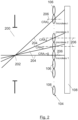
- Plenoptic cameras 100 are commonly composed by a main lens 102 (the upper barrel of optical components or a set of lenses equivalent to said main lens), a plurality of microlenses 106 arranged in a microlens array 104, and an image sensor 108.
- the system is a pupil imaging system, wherein each microlens 106 of the microlens array 104 forms an image of the main aperture of the plenoptic camera over a small area of the image sensor 108.
- Figure 1 shows two bunches of rays (112a, 112b) crossing the main aperture 200 of the plenoptic camera 100, and reaching a central microlens 106a and an adjacent microlens 106b in the array 104, respectively.
- Each bunch (112a, 112b) produces a different microimage (110a, 110b) over the image sensor 108.
- the two microimages (110a, 110b) do not overlap if the optical system is adequately designed.
- the centre of each microimage (110a, 110b) is determined by the corresponding chief ray angle (CRA).
- CRA chief ray angle
- the CRA i is the angle formed between the optical axis 206 of microlens i and the ray 204 that crosses the centre of the aperture 202 or pupil of the optical system and reaches the centre of microlens i.
- Figure 2 illustrates this definition for the example of a linear CRA curve.
- the CRA curve of the microlens array 104 is a discretization (with as many points as the number of microlenses 106) of the continuous CRA curve for the main lens of the system.
- the shape of the microlenses 106 in a 2D frontal view, can be circles (with fill factors below 100%), squares, hexagons or any other shape, offering different advantages and disadvantages for several design criteria.
- the present invention is described using square microlenses; however, this should not be interpreted in a limiting way since the extrapolation to hexagonal, circular or any other shape is straightforward for an expert in the field.
- microlens array 104 Aberrations of the whole optical system may spoil the performance of the device.
- a new design for the microlens array 104 is employed, in which the aberrations of the microlenses (critical part of plenoptic systems) are drastically reduced, aiming to achieve improved performance of plenoptic cameras.
- the microlens arrays herein described, as well as the methods to build them, are not restricted to their use in plenoptic cameras, but can be used in any device containing a microlens array.
- a microlens array 104 is usually a panel containing equally spaced and homogeneous microlenses (with all the lenslets composing the microlens array 104 having exactly the same shape).
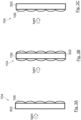
- the microlens array 104 may have different manufacturing options or embodiments that, for manufacturability reasons, may be different to the schematic (and perfect) microlens array 104 shown in Figure 1 .
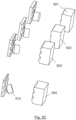
- Figures 3A-3C shows different possible embodiments for microlens arrays 104 comprising a substrate 302 and a plurality of microlenses 106 (the practical implementation of the microlens arrays 104 and the microlenses 106 in real products or prototypes differs from the simplified representation in Figure 1 ).
- the microlenses 106 are usually built or disposed on a substrate 302 with a given width.
- the microlenses 106 shown in Figures 3A-3C are arranged over the substrate 302 and they may be facing the light coming from the left side ( Figure 3C ) or they may be placed at the opposite side such that the light crosses the substrate 302 before hitting the microlenses 106, (as in Figure 3A ).
- the invention might be also implemented with microlenses 106 as shown in Figure 1 or with any other shapes.
- the microlenses 106 may be disposed in the microlens array 104 with a fill factor of 1 or less. Also, the shape of the microlenses 106 may be a unique semi-sphere or composed by four sphere caps in a square microlens, or six sphere caps in hexagonal microlenses, or the conjunction of various sphere caps. Microlenses 106 may also be aspheric lenses.
- the aberrations of the microlens array 104 may degrade the performance of a plenoptic camera.
- the extreme microlenses in a microlens array frequently receive light with a high angle of incidence, which can be even greater than 30 degrees. These high angles of incidence cause very high aberrations in lenslets with only one or two surfaces and specially when, for manufacturability reasons, the usage of aspheres becomes unreliable for the very small dimensions typically adopted in the small mini-cameras of battery operated portable devices with very small dimensions.
- the main lenses have sizes of a few millimetres, apertures are below one millimetre, and the microlenses may reach dimensions as low as a few microns.
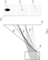
- Figure 4 illustrates the aberrations suffered by a microlens 106 whose optical surface is built at the right side of a substrate 302 when increasing the field angle of collimated light that illuminates the microlens 106 from the left.
- FIG. 4 On the left side of Figure 4 , a schematic view of the microlens 106 and the rays reaching the microlens 106 with an angle of 0 degrees (rays 402), 15 degrees (rays 404) and 30 degrees (rays 406) are depicted.
- the right side of Figure 4 shows the spots (412, 414, 416) produced by the different rays (402, 404, 406) in the best focus plane.
- Rays 402 produce a spot 412, a sharp point, on the best focus plane for a microlens 106 near the optical axis.
- a spot 414 For rays 404 reaching the microlenses at an angle of 15 degrees, a spot 414 is produced, which is not as sharp as spot 412.
- the microlens 106 and its optical properties comply with typical design values for plenoptic cameras (refractive index, radius of curvature, dimensions, etc.). A very good behaviour of the microlens 106 for rays with an angle of incidence of 0 degrees can be observed (completely free of aberrations). However, incoming beams at 15 degrees generate quite badly aberrations, and the performance of the microlens is completely spoiled when the beam has an angle of incidence of 30 degrees.
- the microlenses are adequately tilted or orientated depending on their location within the array to reduce drastically the angle of incidence of the rays and, therefore, in this way minimizing the aberrations of the microlens array and greatly improving the performance of the camera.
- the microlenses can be tilted to reach substantially down to 0 degrees for the CRA of every microlens 106 of the array; hence, for the rays that cross the centre of the aperture 202 of the main lens 102 and reach a microlens 106, it is irrelevant whether the microlens is near the optical axis or at high fields near the limit of the field of view (FOV).
- This phenomenon becomes especially critical in the very small dimensions of mini-cameras for mobile devices where the total track length (TTL) of the camera becomes only a few millimetres and the angles become quite high (values around 30 degrees are quite common, as shown in the example of Figure 7 ).
- all the microlenses 106 would show the same behaviour as that of the central microlenses 106a, being free of most aberration effects.
- each microlens has to be gradually more and more tilted as the field increases. However, at some point at very high fields, the tilt saturates and then starts to minimally decrease (as microlenses are tilted to compensate the effect shown in Figure 7 ).
- Central microlenses 106a do not need to be tilted, and they are more and more tilted as we approach the extreme zones of the panel that contains the microlenses, until the saturation of CRA (zone of saturation 704 in Figure 7 ) is reached and the CRA starts to decrease (fall zone 706 in Figure 7 ), being the microlenses with higher CRA i the most tilted microlenses.
- the microlenses 106 can be tilted until a specific acceptable CRA is reached for every microlens 106 of the microlens array 104. In at least one embodiment, the microlenses 106 can be tilted following any CRA curve specifications (imposed by the main lens 102) to ensure a good performance of the whole plenoptic system.
- Figures 5A-5E show, according to the present invention, an example of a design for the microlens array 104 with tilted microlenses 106, that helps to understand how to design and manufacture microlenses in compliance with the invention. These figures explain a particular embodiment that in no case should be interpreted as a limiting implementation but only a particular embodiment of tilted microlenses. In this particular example, microlenses 106 built on a substrate 302 are used.
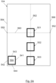
- Figure 5A shows a 2D view of the microlens array 104 panel with four different highlighted zones (a central zone 501, a middle lower zone 502, an extreme lower zone 503 and a corner zone 504), each zone comprising one or more microlenses 106 designed with a specific tilt.
- Figures 5B , 5C and 5D show three 3D views of the designed tilted microlenses 106 built for the four zones (501, 502, 503, 504) specified in Figure 5A , each highlighted zone comprising a matrix (one or more rows, and one or more columns) of tilted microlenses 106.
- the optical axes 206 of the microlenses in a regular (i.e. not tilted) microlens array are parallel to axis z in Figure 5B .
- optical axis 206 of microlenses in the microlens array of the present invention rotate a certain angle ⁇ vs axis x and z as we move vertically along line 562 (as depicted in the example of Figure 5B ) and a certain angle ⁇ vs axis y and z as we move horizontally depending, on their location within the array; in other positions not directly over lines 560 and 562, such as corner zone 504, both angles ⁇ and ⁇ are not equal to zero.
- Figure 5B also depicts an example of a stamping tool 510 (e.g. a cylinder with different tilts) used to produce manufacturing molds 520 which in turn can be employed to manufacture microlenses 106 with different tilts over different areas 501, 502, 503, 504 of the substrate.
- the mould 520 is used to build the tilted microlenses depending on the particular zone of the microlens array 104 panel.
- Figure 5E shows a schematic 2D view of the example embodiment of Figures 5A-D .
- the microlenses 106 are tilted with different tilting degrees ( ⁇ 1 , ⁇ 2 , ⁇ 3 , ..., ⁇ i ) around their optical axis 206 depending on their location in the array.
- a tilted microlens can be understood as a lens in which the vertex and the optical centre are not located at the same position with respect to the plane 108; thus, tilting the microlenses is equivalent to shifting the vertex of the microlens along axis x and y until a specific CRAi is reached for the microlens i.
- tilting degree ⁇ 2 for microlenses in the middle lower zone 502 is smaller than tilting degree ⁇ 3 for microlenses in the extreme lower zone 503, as shown in Figures 5B and 5E ).
- the maximum tilt of ⁇ and ⁇ is built for the corners of the microlens array 104 panel, corresponding to the corner zone 504. Nevertheless, in an embodiment the maximum tilt is actually not built for the extreme microlenses of said corner zone 504, but for inner microlenses still approaching the corner zone 504 of the panel.
- Figures 5B-5D also shows an example of a possible way to manufacture the mould to build the microlens array 104.
- a stamping tool 510 is used to build a mould 520, over which liquid optical polymers can be deposited, that are later solidified (with UV-light or any other procedure).
- stamping, milling, grinding, etching or other tools may be used in order to build the moulds and the tilted microlenses.
- other techniques as reactive ion etching and many other may be used, including optical manufacturing techniques similar to the techniques used for silicon manufacturing. The particular description of the figures should not be interpreted as a limiting factor.
- Photo-sensors are extremely efficient when they receive light reaching the sensor perpendicular to the photosensitive surface, but their quantum-efficiency (related to the amount of current or electrical-energy generated by a given amount of incident light-energy) deteriorates when the light beams reach the photosensitive surface at an angle.
- the angle of incidence of the light beams over the image sensor 108 must be limited by the lens design (to avoid the quantum efficiency losses just mentioned and crosstalk between neighbouring pixels).
- the optical design of the upper lens and the sensor design are conceived to match each other: the aspheric surfaces used in the main lens design cause that the angle of arrival of light beams to the image-sensor for different field values is very nonlinear (as shown in the curve 700 in Figure 7 ), and the sensor design is equally optimized to have the maximum quantum efficiency for precisely those same angles of arrival.
- the sensors are designed in a way that every pixel (every individual photosensitive surface) has a pixel-microlens that concentrates the light beam on the central photosensitive area of every pixel.
- small mini-cameras have a CRA-curve of the main lens (or of the upper barrel equivalent lens) similar to 700 in Figure 7 , the design of the sensor places the pixel-microlenses with a different pitch (smaller) than the pixel pitch, optimizing the sensor for the expected angles of incidence of light coming from optics with very small mechanical total track lengths (MTTL) and hence large angles of arrival for large fields.
- MTTL mechanical total track lengths
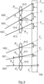
- the image sensor 108 gathers a collection of microimages, each microimage formed by every one of the microlenses 106.
- the location of these microimages over the image sensor 108 depends on the CRA curve (curves 700 or 710 in Figure 7 ); more specifically, the centre of each microimage will be determined by the corresponding CRA i , the CRA of each microlens i of the microlens array 104.
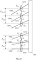
- Figure 6 shows this dependence.
- CRA are depicted for a first 610 microlens, a second 611 microlens, a third 612 microlens, an (i-1)-th microlens 613, an i-th microlens 614, and an (i+1)-th microlens 615.
- T i refers to the location of the centre of microimage i
- P i refers to the location of the centre of microlens i (614)
- f ul refers to the focal length of the microlenses (assuming all microlenses have the same focal length). It is evident that the equation above is valid for any CRA curve.
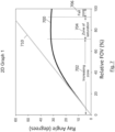
- Figure 7 shows an example of a typical CRA curve 700 for a specific optical design for illustrative purposes and should not be taken as a limitation.
- the CRA curve 700 is divided into three different regions or zones: a first and larger region, increasing zone 702, in which the CRA increases with the field until reaching a second region for high fields (in the example, around 70%-90% relative FOV), zone of saturation 704, in which the CRA remains substantially constant with the field; and a third and small region in the extreme fields (in the example, more than 90% relative FOV), fall zone 706, in which the CRA decreases with the field.
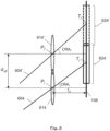
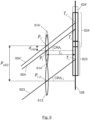
- FIG 8 two microlenses (614, 614') and the two corresponding microimages (624, 624') over the image sensor 108 are shown.
- microimage 624 will be centred in a position which is different from the position (given by equation 2) that it would had been centred (microimage 624') should the system had shown a linear CRA curve 710.
- the centre P i of the microlens i (614) needs to be displaced a certain distance d ul(i) (and thus, change the pitch to P ul ( i ) for this particular microlens i) to the position corresponding to the centre P i ' of microlens i' (614'); that is, P i moves to P i ' in Figure 8 so that the centre T i of microimage 624 moves to the centre T i ' of microimage 624' produced by ray 604'.
- Figure 9 represents an example similar with that of Figure 8 (although with a shorter displacement d ul(i) ) considering the adjacent microlens i-1 (613), in which the centre P i of microlens i (614) is displaced a distance d ul(i) .
- the original and constant pitch P ul is increased to a new pitch P ul(i) for microlens i.
- Microimage 624 of microlens i moves to microimage 624', so that microimages of consecutive microlenses (613, 614') do not overlap.
- these interstitial spaces are filled by increasing the size of the microlenses, as in the example of Figure 11 showing microlenses (1110, 1111, 1112, 1113, 1114, 1115) with increasing diameters (D i+1 >D i >D i-1 >D 3 >D 2 >D 1 ).
- at least one opaque layer covering the edges of adjacent microlenses may be applied.
- the opaque layers which are made of a material that do not allow light to go through, not only avoid the possible imperfections of the edges between microlenses (which disappear as far as optical flow of light is concerned), but also take profit of the well know effect that lenses are nearer the paraxial approximation if we restrict the flow of light at their edges and exhibit less aberrations if their edges are avoided with additional apertures (in this case the apertures are produced by the opaque layer).
- the morphology of each microlens is not necessarily symmetric with respect to its centre.
- the shape of the microlenses (especially at the corners of the microlens array 104) is no longer a regular square but a non-regular four-side polygon.
- the important factor is that the optical centres of the microlenses 106 are designed such that the optical behaviour of real main lenses (as in Figure 7 ) with real microlenses (as in Figure 4 ) becomes the same as if we had used a paraxial main lens and paraxial lenslets.
- Another possible embodiment is to reduce the fill factor of the microlens array.
- the morphology of every one of the microlenses can be kept symmetric.
- the microlenses are tilted conveniently, the angle of incidence of the rays on the microlenses surface is reduced, reducing the aberrations; likewise, if the pitches are changed conveniently, the centres of the microimages will be located as in a paraxial system (the microlenses are adapted to the main lens CRA).
- the microlens array may be designed with variable tilt, with variable pitch, or with a combination of both depending on the specific requirements of the particular embodiment.
- variable pitch and variable tilt the design and performance analysis to obtain the exact tilting degrees and pitch values must be performed together, as the tilted microlenses may affect the variable pitch design and vice versa.
- the degree of tilting for the microlenses as field increases (until the zone of saturation 704 is reached and beyond), ii) the particular CRA curves of the microlens surfaces, which not only depend on the physical parameters of the microlens itself but also on the direction of arrival of light from the main lens, and iii) the pace to increase pitches (and optionally sizes) of microlenses as field increases; are all closely related to the deviations of the main lens of the camera from the paraxial behaviour, and more specifically to the CRA non-linear behaviour (as exemplified in Figure 7 ) and to other aberrations of the main lens.
- lenslet tilting, lenslet surface equations, pitch and size of lenslets as the field increases are closely related to the specific design of any particular main lens and it will be evident for an expert optical designer how to trade-off and design all those factors as related to any particular embodiment of the main lens.
Landscapes
- Physics & Mathematics (AREA)
- General Physics & Mathematics (AREA)
- Optics & Photonics (AREA)
- Studio Devices (AREA)
- Lenses (AREA)
Claims (12)
- Lichtfelderfassungsvorrichtung umfassend ein optisches System, wobei das optische System eine Hauptlinse (102), einen Bildsensor (108) und eine Mikrolinsenanordnung (104) umfasst, umfassend eine Vielzahl von Mikrolinsen (106), wobei die Zentren der Mikrolinsen (106) der Mikrolinsenanordnung (104) um einen bestimmten Abstand (d u/(i) ) von einer regelmäßigen Anordnung mit einer konstanten Teilung Pul derart verschoben sind, dass benachbarte Mikrolinsen in Kontakt stehen, wobei der verschobene Abstand (dul(i)) in einer zentralen Zone (501) der Mikrolinsenanordnung (104) null ist,
dadurch gekennzeichnet, dassdie Teilung zwischen Zentren von Mikrolinsen (106) allmählich vergrößert wird, wenn das Sichtfeld sich vergrößert, bis zu einer vergrößerten neuen Teilung P ul(i) für die Mikrolinse i, die größer ist als die konstante Teilung Pul, um die Nichtlinearitäten des Hauptstrahlwinkels mit dem Sichtfeld auszugleichen;wobei die Größe einer Vielzahl von Mikrolinsen (106) der Mikrolinsenanordnung (104) von dem Abstand zur Mitte der Mikrolinsenanordnung (104) abhängt, wobei die Größen der Mikrolinsen (106) derart vergrößert werden, dass die Zwischenräume (gi ) zwischen benachbarten Mikrolinsen gefüllt werden. - Lichtfelderfassungsvorrichtung nach Anspruch 1, wobei die vergrößerte neue Teilung Pul(i) für die Mikrolinse i derart ist, dass die von den Mikrolinsen (106) generierten Mikrobilder gleichmäßig über den Bildsensor (108) verteilt sind und die Mikrobilder aufeinanderfolgender Mikrolinsen sich nicht überlappen.
- Lichtfelderfassungsvorrichtung nach Anspruch 1, wobei die Größen der Mikrolinsen (106) derart sind, dass der Füllfaktor der Mikrolinsenanordnung (104) im Wesentlichen 1 beträgt.
- Lichtfelderfassungsvorrichtung nach einem der vorhergehenden Ansprüche, ferner umfassend mindestens eine lichtundurchlässige Schicht, die die Kanten benachbarter Mikrolinsen abdeckt.
- Lichtfelderfassungsvorrichtung nach einem der vorhergehenden Ansprüche, wobei eine Vielzahl von Mikrolinsen (106) der Mikrolinsenanordnung (104) in Abhängigkeit vom Abstand zwischen der Mikrolinse (106) und der Mitte der Mikrolinsenanordnung (104) um einen Kippgrad (α, β) in Bezug auf die optische Achse der Hauptlinse (102) gekippt ist.
- Lichtfelderfassungsvorrichtung nach Anspruch 5, wobei sich mindestens eine Komponente des Kippgrades (α, β) mit dem Abstand zwischen der Mikrolinse (106) und der Mitte der Mikrolinsenanordnung (104) vergrößert, wobei diese Bedingung mindestens in einer Zone der Mikrolinsenanordnung (104) erfüllt ist.
- Lichtfelderfassungsvorrichtung nach einem der Ansprüche 5 bis 6, wobei die Mikrolinsen (106) auf einem Substrat (302) aufgebaut sind.
- Lichtfelderfassungsvorrichtung nach einem der Ansprüche 5 bis 7, wobei die Mikrolinsen (106) mit Kippgraden (α, β) ausgelegt sind, die den Hauptstrahlwinkel der Mikrolinsen (106) reduzieren, wobei der Hauptstrahlwinkel (CRAi) einer Mikrolinse i der Winkel ist, der zwischen der optischen Achse (206) der Mikrolinse i und dem Strahl (204) gebildet wird, der das Zentrum der Öffnung (202) des optischen Systems kreuzt und die Mitte der Mikrolinse i erreicht.
- Lichtfelderfassungsvorrichtung nach Anspruch 8, wobei die Mikrolinsen (106) mit Kippgraden (α, β) ausgelegt sind, die die Nichtlinearitäten zwischen der Feldposition und dem Hauptstrahlwinkel der Mikrolinsen (106) ausgleichen.
- Lichtfelderfassungsvorrichtung nach einem der Ansprüche 8 bis 9, wobei die Kippgrade (α, β) der Mikrolinsen (106) derart sind, dass der Hauptstrahlwinkel der entsprechenden Mikrolinse (106) kleiner als ein vorbestimmter Schwellenwert ist.
- Lichtfelderfassungsvorrichtung nach Anspruch 10, wobei die Kippgrade (α, β) der Mikrolinsen (106) derart sind, dass der Hauptstrahlwinkel der entsprechenden Mikrolinse (106) im Wesentlichen 0 Grad beträgt.
- Lichtfelderfassungsvorrichtung nach einem der vorhergehenden Ansprüche, wobei die Lichtfelderfassungsvorrichtung eine plenoptische Kamera (100) ist.
Applications Claiming Priority (1)
| Application Number | Priority Date | Filing Date | Title |
|---|---|---|---|
| PCT/EP2016/079787 WO2018103819A1 (en) | 2016-12-05 | 2016-12-05 | Microlens array |
Publications (3)
| Publication Number | Publication Date |
|---|---|
| EP3548935A1 EP3548935A1 (de) | 2019-10-09 |
| EP3548935C0 EP3548935C0 (de) | 2024-08-28 |
| EP3548935B1 true EP3548935B1 (de) | 2024-08-28 |
Family
ID=57482443
Family Applications (1)
| Application Number | Title | Priority Date | Filing Date |
|---|---|---|---|
| EP16805846.9A Active EP3548935B1 (de) | 2016-12-05 | 2016-12-05 | Lichtfelderfassungsgerät |
Country Status (5)
| Country | Link |
|---|---|
| US (1) | US11099304B2 (de) |
| EP (1) | EP3548935B1 (de) |
| JP (1) | JP6947438B2 (de) |
| CN (1) | CN110192127B (de) |
| WO (1) | WO2018103819A1 (de) |
Families Citing this family (10)
| Publication number | Priority date | Publication date | Assignee | Title |
|---|---|---|---|---|
| US10999540B1 (en) * | 2019-04-03 | 2021-05-04 | Apple Inc. | Camera with asymmetric field of view |
| DE102019207867A1 (de) * | 2019-05-29 | 2020-12-03 | Robert Bosch Gmbh | Optische Anordnung mit einem verbesserten Aberrationsverhalten und LIDAR-Vorrichtung mit einer derartigen Anordnung |
| CN110764249B (zh) * | 2019-10-29 | 2022-05-17 | Oppo广东移动通信有限公司 | 图像传感器、摄像模组及终端设备 |
| CN110554448A (zh) * | 2019-09-10 | 2019-12-10 | 吉林大学 | 一种大眼曲率可调的人工复眼、制备方法及应用 |
| DE102019126982A1 (de) * | 2019-10-08 | 2021-04-08 | Sick Ag | Optoelektronischer Sensor und Verfahren zur Erfassung von Objekten |
| CN112824941A (zh) * | 2019-11-21 | 2021-05-21 | 南昌欧菲生物识别技术有限公司 | 微透镜阵列元件以及扩散片和电子设备 |
| CN112415736B (zh) * | 2020-11-24 | 2023-06-06 | 深圳技术大学 | 光场光学显微镜及光场光学显微系统 |
| CN117769841A (zh) * | 2022-07-21 | 2024-03-26 | 北京小米移动软件有限公司 | 拍摄装置以及控制方法 |
| CN115327846B (zh) * | 2022-08-12 | 2024-09-06 | 华天慧创科技(西安)有限公司 | 一种消除微透镜阵列旁瓣的照明系统的设计方法 |
| CN118050834A (zh) * | 2022-11-16 | 2024-05-17 | 华为技术有限公司 | 一种透镜阵列及电子设备 |
Family Cites Families (16)
| Publication number | Priority date | Publication date | Assignee | Title |
|---|---|---|---|---|
| US5731899A (en) * | 1996-12-20 | 1998-03-24 | Eastman Kodak Company | Lenslet array system incorporating an integral field lens/reimager lenslet array |
| DE102004003013B3 (de) * | 2004-01-20 | 2005-06-02 | Fraunhofer-Gesellschaft zur Förderung der angewandten Forschung e.V. | Bilderfassungssystem und dessen Verwendung |
| CN101426085B (zh) * | 2004-10-01 | 2012-10-03 | 小利兰·斯坦福大学托管委员会 | 成像装置及其方法 |
| EP2398223B1 (de) * | 2004-10-01 | 2014-03-19 | The Board Of Trustees Of The Leland Stanford Junior University | Bilderzeugungsanordnung und -verfahren |
| KR100693927B1 (ko) * | 2005-02-03 | 2007-03-12 | 삼성전자주식회사 | 마이크로 렌즈 제조방법, 마이크로 렌즈 어레이 제조방법및 이미지 센서 제조방법 |
| US7796180B2 (en) * | 2005-08-03 | 2010-09-14 | Aptina Imaging Corporation | Method for calculating circular symmetrical microlens/color filter array shift |
| US7687757B1 (en) * | 2009-01-29 | 2010-03-30 | Visera Technologies Company Limited | Design of microlens on pixel array |
| JP5463718B2 (ja) * | 2009-04-16 | 2014-04-09 | ソニー株式会社 | 撮像装置 |
| DE102009049387B4 (de) * | 2009-10-14 | 2016-05-25 | Fraunhofer-Gesellschaft zur Förderung der angewandten Forschung e.V. | Vorrichtung, Bildverarbeitungsvorrichtung und Verfahren zur optischen Abbildung |
| GB2488519A (en) * | 2011-02-16 | 2012-09-05 | St Microelectronics Res & Dev | Multi-channel image sensor incorporating lenslet array and overlapping fields of view. |
| GB2501936B (en) * | 2012-05-11 | 2016-11-30 | Canon Kk | Micro lens array and imaging apparatus |
| KR20140094395A (ko) * | 2013-01-22 | 2014-07-30 | 삼성전자주식회사 | 복수 개의 마이크로렌즈를 사용하여 촬영하는 촬영 장치 및 그 촬영 방법 |
| JP5791664B2 (ja) * | 2013-06-28 | 2015-10-07 | キヤノン株式会社 | 光学素子アレイ、及び固体撮像装置 |
| JP6126474B2 (ja) * | 2013-06-28 | 2017-05-10 | キヤノン株式会社 | 撮像装置及びその制御方法 |
| JP2015185998A (ja) * | 2014-03-24 | 2015-10-22 | 株式会社東芝 | 画像処理方法および撮像装置 |
| JP5721891B2 (ja) * | 2014-08-01 | 2015-05-20 | キヤノン株式会社 | 撮像装置 |
-
2016
- 2016-12-05 EP EP16805846.9A patent/EP3548935B1/de active Active
- 2016-12-05 US US16/466,439 patent/US11099304B2/en active Active
- 2016-12-05 JP JP2019549633A patent/JP6947438B2/ja active Active
- 2016-12-05 WO PCT/EP2016/079787 patent/WO2018103819A1/en not_active Ceased
- 2016-12-05 CN CN201680092018.6A patent/CN110192127B/zh active Active
Non-Patent Citations (1)
| Title |
|---|
| EDMUND Y. LAM: "Computational photography with plenoptic camera and light field capture: tutorial", JOURNAL OF THE OPTICAL SOCIETY OF AMERICA A, vol. 32, no. 11, 14 October 2015 (2015-10-14), pages 2021, XP055553906, ISSN: 1084-7529, DOI: 10.1364/JOSAA.32.002021 * |
Also Published As
| Publication number | Publication date |
|---|---|
| EP3548935C0 (de) | 2024-08-28 |
| US20200064522A1 (en) | 2020-02-27 |
| CN110192127B (zh) | 2021-07-09 |
| EP3548935A1 (de) | 2019-10-09 |
| JP2020513597A (ja) | 2020-05-14 |
| JP6947438B2 (ja) | 2021-10-13 |
| CN110192127A (zh) | 2019-08-30 |
| WO2018103819A1 (en) | 2018-06-14 |
| US11099304B2 (en) | 2021-08-24 |
Similar Documents
| Publication | Publication Date | Title |
|---|---|---|
| EP3548935B1 (de) | Lichtfelderfassungsgerät | |
| JP7060482B2 (ja) | ニアアイライトフィールド表示装置及びニアアイ表示装置 | |
| ES2466820T3 (es) | Dispositivo de procesamiento de imágenes | |
| US10007122B2 (en) | Three-dimensional display substrate, its Manufacturing method and three-dimensional display device | |
| US9372349B2 (en) | Glasses-free 3D display for multiple viewers with a resonant subwavelength lens layer | |
| KR102349765B1 (ko) | 몰입형 컴팩트 디스플레이 안경 | |
| KR102428834B1 (ko) | 표시 장치 | |
| US20130135515A1 (en) | Digital imaging system | |
| CN101449193A (zh) | 具有波前编码的变焦透镜系统 | |
| US20130182319A1 (en) | Three-dimensional image display panel structure | |
| CN109471267B (zh) | 一种激光匀化器 | |
| CN111624784A (zh) | 一种光场显示装置 | |
| KR20120018370A (ko) | 무안경 입체식 디스플레이 디바이스 | |
| GB2501936A (en) | Micro-lens array with micro-lens subsets displaced from a regular lattice pattern | |
| KR20100059896A (ko) | 이미지 센서 | |
| WO2024012232A1 (en) | Three-dimensional integral-imaging light field display and optimization method therefor | |
| WO2021243037A1 (en) | System and method for holographic displays | |
| RU2694781C2 (ru) | Многовидовое устройство отображения | |
| EP3312642B1 (de) | Planare varifokuslinse | |
| US20220171206A1 (en) | Display apparatus, vr apparatus and display method | |
| CN114035250A (zh) | 变焦液晶透镜、驱动方法及显示装置 | |
| CN113514988B (zh) | 变焦液晶透镜及其驱动方法 | |
| WO2024193151A1 (zh) | 三维显示装置及系统 | |
| Takaki et al. | Flat panel display with slanted pixel arrangement for 16-view display | |
| EP3104593A1 (de) | Lichtfeldabbildungsvorrichtung |
Legal Events
| Date | Code | Title | Description |
|---|---|---|---|
| STAA | Information on the status of an ep patent application or granted ep patent |
Free format text: STATUS: UNKNOWN |
|
| STAA | Information on the status of an ep patent application or granted ep patent |
Free format text: STATUS: THE INTERNATIONAL PUBLICATION HAS BEEN MADE |
|
| PUAI | Public reference made under article 153(3) epc to a published international application that has entered the european phase |
Free format text: ORIGINAL CODE: 0009012 |
|
| STAA | Information on the status of an ep patent application or granted ep patent |
Free format text: STATUS: REQUEST FOR EXAMINATION WAS MADE |
|
| 17P | Request for examination filed |
Effective date: 20190612 |
|
| AK | Designated contracting states |
Kind code of ref document: A1 Designated state(s): AL AT BE BG CH CY CZ DE DK EE ES FI FR GB GR HR HU IE IS IT LI LT LU LV MC MK MT NL NO PL PT RO RS SE SI SK SM TR |
|
| AX | Request for extension of the european patent |
Extension state: BA ME |
|
| DAV | Request for validation of the european patent (deleted) | ||
| DAX | Request for extension of the european patent (deleted) | ||
| RAP3 | Party data changed (applicant data changed or rights of an application transferred) |
Owner name: PHOTONIC SENSORS & ALGORITHMS, S.L. |
|
| STAA | Information on the status of an ep patent application or granted ep patent |
Free format text: STATUS: EXAMINATION IS IN PROGRESS |
|
| 17Q | First examination report despatched |
Effective date: 20220330 |
|
| GRAP | Despatch of communication of intention to grant a patent |
Free format text: ORIGINAL CODE: EPIDOSNIGR1 |
|
| STAA | Information on the status of an ep patent application or granted ep patent |
Free format text: STATUS: GRANT OF PATENT IS INTENDED |
|
| INTG | Intention to grant announced |
Effective date: 20240409 |
|
| GRAS | Grant fee paid |
Free format text: ORIGINAL CODE: EPIDOSNIGR3 |
|
| GRAA | (expected) grant |
Free format text: ORIGINAL CODE: 0009210 |
|
| STAA | Information on the status of an ep patent application or granted ep patent |
Free format text: STATUS: THE PATENT HAS BEEN GRANTED |
|
| AK | Designated contracting states |
Kind code of ref document: B1 Designated state(s): AL AT BE BG CH CY CZ DE DK EE ES FI FR GB GR HR HU IE IS IT LI LT LU LV MC MK MT NL NO PL PT RO RS SE SI SK SM TR |
|
| REG | Reference to a national code |
Ref country code: GB Ref legal event code: FG4D |
|
| REG | Reference to a national code |
Ref country code: CH Ref legal event code: EP |
|
| REG | Reference to a national code |
Ref country code: DE Ref legal event code: R096 Ref document number: 602016089140 Country of ref document: DE |
|
| REG | Reference to a national code |
Ref country code: IE Ref legal event code: FG4D |
|
| U01 | Request for unitary effect filed |
Effective date: 20240913 |
|
| U07 | Unitary effect registered |
Designated state(s): AT BE BG DE DK EE FI FR IT LT LU LV MT NL PT RO SE SI Effective date: 20241015 |
|
| PG25 | Lapsed in a contracting state [announced via postgrant information from national office to epo] |
Ref country code: NO Free format text: LAPSE BECAUSE OF FAILURE TO SUBMIT A TRANSLATION OF THE DESCRIPTION OR TO PAY THE FEE WITHIN THE PRESCRIBED TIME-LIMIT Effective date: 20241128 |
|
| PG25 | Lapsed in a contracting state [announced via postgrant information from national office to epo] |
Ref country code: GR Free format text: LAPSE BECAUSE OF FAILURE TO SUBMIT A TRANSLATION OF THE DESCRIPTION OR TO PAY THE FEE WITHIN THE PRESCRIBED TIME-LIMIT Effective date: 20241129 Ref country code: PL Free format text: LAPSE BECAUSE OF FAILURE TO SUBMIT A TRANSLATION OF THE DESCRIPTION OR TO PAY THE FEE WITHIN THE PRESCRIBED TIME-LIMIT Effective date: 20240828 |
|
| U20 | Renewal fee for the european patent with unitary effect paid |
Year of fee payment: 9 Effective date: 20241217 |
|
| PG25 | Lapsed in a contracting state [announced via postgrant information from national office to epo] |
Ref country code: IS Free format text: LAPSE BECAUSE OF FAILURE TO SUBMIT A TRANSLATION OF THE DESCRIPTION OR TO PAY THE FEE WITHIN THE PRESCRIBED TIME-LIMIT Effective date: 20241228 |
|
| PG25 | Lapsed in a contracting state [announced via postgrant information from national office to epo] |
Ref country code: HR Free format text: LAPSE BECAUSE OF FAILURE TO SUBMIT A TRANSLATION OF THE DESCRIPTION OR TO PAY THE FEE WITHIN THE PRESCRIBED TIME-LIMIT Effective date: 20240828 |
|
| PG25 | Lapsed in a contracting state [announced via postgrant information from national office to epo] |
Ref country code: RS Free format text: LAPSE BECAUSE OF FAILURE TO SUBMIT A TRANSLATION OF THE DESCRIPTION OR TO PAY THE FEE WITHIN THE PRESCRIBED TIME-LIMIT Effective date: 20241128 Ref country code: ES Free format text: LAPSE BECAUSE OF FAILURE TO SUBMIT A TRANSLATION OF THE DESCRIPTION OR TO PAY THE FEE WITHIN THE PRESCRIBED TIME-LIMIT Effective date: 20240828 |
|
| PG25 | Lapsed in a contracting state [announced via postgrant information from national office to epo] |
Ref country code: RS Free format text: LAPSE BECAUSE OF FAILURE TO SUBMIT A TRANSLATION OF THE DESCRIPTION OR TO PAY THE FEE WITHIN THE PRESCRIBED TIME-LIMIT Effective date: 20241128 Ref country code: PL Free format text: LAPSE BECAUSE OF FAILURE TO SUBMIT A TRANSLATION OF THE DESCRIPTION OR TO PAY THE FEE WITHIN THE PRESCRIBED TIME-LIMIT Effective date: 20240828 Ref country code: NO Free format text: LAPSE BECAUSE OF FAILURE TO SUBMIT A TRANSLATION OF THE DESCRIPTION OR TO PAY THE FEE WITHIN THE PRESCRIBED TIME-LIMIT Effective date: 20241128 Ref country code: IS Free format text: LAPSE BECAUSE OF FAILURE TO SUBMIT A TRANSLATION OF THE DESCRIPTION OR TO PAY THE FEE WITHIN THE PRESCRIBED TIME-LIMIT Effective date: 20241228 Ref country code: HR Free format text: LAPSE BECAUSE OF FAILURE TO SUBMIT A TRANSLATION OF THE DESCRIPTION OR TO PAY THE FEE WITHIN THE PRESCRIBED TIME-LIMIT Effective date: 20240828 Ref country code: GR Free format text: LAPSE BECAUSE OF FAILURE TO SUBMIT A TRANSLATION OF THE DESCRIPTION OR TO PAY THE FEE WITHIN THE PRESCRIBED TIME-LIMIT Effective date: 20241129 Ref country code: ES Free format text: LAPSE BECAUSE OF FAILURE TO SUBMIT A TRANSLATION OF THE DESCRIPTION OR TO PAY THE FEE WITHIN THE PRESCRIBED TIME-LIMIT Effective date: 20240828 |
|
| PG25 | Lapsed in a contracting state [announced via postgrant information from national office to epo] |
Ref country code: SM Free format text: LAPSE BECAUSE OF FAILURE TO SUBMIT A TRANSLATION OF THE DESCRIPTION OR TO PAY THE FEE WITHIN THE PRESCRIBED TIME-LIMIT Effective date: 20240828 |
|
| PG25 | Lapsed in a contracting state [announced via postgrant information from national office to epo] |
Ref country code: CZ Free format text: LAPSE BECAUSE OF FAILURE TO SUBMIT A TRANSLATION OF THE DESCRIPTION OR TO PAY THE FEE WITHIN THE PRESCRIBED TIME-LIMIT Effective date: 20240828 |
|
| PG25 | Lapsed in a contracting state [announced via postgrant information from national office to epo] |
Ref country code: SK Free format text: LAPSE BECAUSE OF FAILURE TO SUBMIT A TRANSLATION OF THE DESCRIPTION OR TO PAY THE FEE WITHIN THE PRESCRIBED TIME-LIMIT Effective date: 20240828 |
|
| PLBE | No opposition filed within time limit |
Free format text: ORIGINAL CODE: 0009261 |
|
| STAA | Information on the status of an ep patent application or granted ep patent |
Free format text: STATUS: NO OPPOSITION FILED WITHIN TIME LIMIT |
|
| PG25 | Lapsed in a contracting state [announced via postgrant information from national office to epo] |
Ref country code: MC Free format text: LAPSE BECAUSE OF FAILURE TO SUBMIT A TRANSLATION OF THE DESCRIPTION OR TO PAY THE FEE WITHIN THE PRESCRIBED TIME-LIMIT Effective date: 20240828 |
|
| REG | Reference to a national code |
Ref country code: CH Ref legal event code: PL |
|
| 26N | No opposition filed |
Effective date: 20250530 |
|
| GBPC | Gb: european patent ceased through non-payment of renewal fee |
Effective date: 20241205 |
|
| PG25 | Lapsed in a contracting state [announced via postgrant information from national office to epo] |
Ref country code: GB Free format text: LAPSE BECAUSE OF NON-PAYMENT OF DUE FEES Effective date: 20241205 |
|
| PG25 | Lapsed in a contracting state [announced via postgrant information from national office to epo] |
Ref country code: CH Free format text: LAPSE BECAUSE OF NON-PAYMENT OF DUE FEES Effective date: 20241231 |
|
| PG25 | Lapsed in a contracting state [announced via postgrant information from national office to epo] |
Ref country code: IE Free format text: LAPSE BECAUSE OF NON-PAYMENT OF DUE FEES Effective date: 20241205 |