EP3547802B1 - Appareil d'éclairage comprenant des diodes électroluminescentes - Google Patents
Appareil d'éclairage comprenant des diodes électroluminescentes Download PDFInfo
- Publication number
- EP3547802B1 EP3547802B1 EP19165826.9A EP19165826A EP3547802B1 EP 3547802 B1 EP3547802 B1 EP 3547802B1 EP 19165826 A EP19165826 A EP 19165826A EP 3547802 B1 EP3547802 B1 EP 3547802B1
- Authority
- EP
- European Patent Office
- Prior art keywords
- led
- voltage
- current
- driving
- stg1
- Prior art date
- Legal status (The legal status is an assumption and is not a legal conclusion. Google has not performed a legal analysis and makes no representation as to the accuracy of the status listed.)
- Active
Links
- 101100311249 Schizosaccharomyces pombe (strain 972 / ATCC 24843) stg1 gene Proteins 0.000 claims description 64
- JPKJQBJPBRLVTM-OSLIGDBKSA-N (2s)-2-amino-n-[(2s,3r)-3-hydroxy-1-[[(2s)-1-[[(2s)-1-[[(2s)-1-[[(2r)-1-(1h-indol-3-yl)-3-oxopropan-2-yl]amino]-1-oxo-3-phenylpropan-2-yl]amino]-1-oxo-3-phenylpropan-2-yl]amino]-1-oxo-3-phenylpropan-2-yl]amino]-1-oxobutan-2-yl]-6-iminohexanamide Chemical compound C([C@H](NC(=O)[C@@H](NC(=O)[C@@H](N)CCCC=N)[C@H](O)C)C(=O)N[C@@H](CC=1C=CC=CC=1)C(=O)N[C@@H](CC=1C=CC=CC=1)C(=O)N[C@H](CC=1C2=CC=CC=C2NC=1)C=O)C1=CC=CC=C1 JPKJQBJPBRLVTM-OSLIGDBKSA-N 0.000 claims description 24
- 102100031277 Calcineurin B homologous protein 1 Human genes 0.000 claims description 24
- 241000839426 Chlamydia virus Chp1 Species 0.000 claims description 24
- 101000777252 Homo sapiens Calcineurin B homologous protein 1 Proteins 0.000 claims description 24
- 101000943802 Homo sapiens Cysteine and histidine-rich domain-containing protein 1 Proteins 0.000 claims description 24
- 238000006243 chemical reaction Methods 0.000 claims description 17
- 102100031272 Calcineurin B homologous protein 2 Human genes 0.000 claims description 11
- 241001510512 Chlamydia phage 2 Species 0.000 claims description 11
- 101000777239 Homo sapiens Calcineurin B homologous protein 2 Proteins 0.000 claims description 11
- 239000010410 layer Substances 0.000 description 26
- 108010064535 CCAAT-Enhancer-Binding Protein-beta Proteins 0.000 description 22
- 102100031051 Cysteine and glycine-rich protein 1 Human genes 0.000 description 22
- 101710185487 Cysteine and glycine-rich protein 1 Proteins 0.000 description 22
- 102100031621 Cysteine and glycine-rich protein 2 Human genes 0.000 description 22
- 239000003990 capacitor Substances 0.000 description 20
- 239000013256 coordination polymer Substances 0.000 description 18
- 102100036791 Adhesion G protein-coupled receptor L2 Human genes 0.000 description 16
- 101000928189 Homo sapiens Adhesion G protein-coupled receptor L2 Proteins 0.000 description 16
- 238000010586 diagram Methods 0.000 description 13
- 230000007423 decrease Effects 0.000 description 12
- 102100036793 Adhesion G protein-coupled receptor L3 Human genes 0.000 description 10
- 101000928176 Homo sapiens Adhesion G protein-coupled receptor L3 Proteins 0.000 description 10
- 101100521063 Arabidopsis thaliana PRD3 gene Proteins 0.000 description 8
- 239000000463 material Substances 0.000 description 7
- 230000003247 decreasing effect Effects 0.000 description 6
- 238000000034 method Methods 0.000 description 6
- 230000006870 function Effects 0.000 description 5
- 101150054516 PRD1 gene Proteins 0.000 description 4
- 101100459905 Saccharomyces cerevisiae (strain ATCC 204508 / S288c) NCP1 gene Proteins 0.000 description 4
- 239000000758 substrate Substances 0.000 description 4
- 101100238374 Arabidopsis thaliana MPS1 gene Proteins 0.000 description 3
- 101150040982 DID4 gene Proteins 0.000 description 3
- 230000008859 change Effects 0.000 description 3
- 238000004519 manufacturing process Methods 0.000 description 3
- 101100123053 Arabidopsis thaliana GSH1 gene Proteins 0.000 description 2
- 101100298888 Arabidopsis thaliana PAD2 gene Proteins 0.000 description 2
- 102100027364 Cysteine-rich protein 3 Human genes 0.000 description 2
- 101000590281 Homo sapiens 26S proteasome non-ATPase regulatory subunit 14 Proteins 0.000 description 2
- 101001114059 Homo sapiens Protein-arginine deiminase type-1 Proteins 0.000 description 2
- 101100471831 Neurospora crassa (strain ATCC 24698 / 74-OR23-1A / CBS 708.71 / DSM 1257 / FGSC 987) rpl-5 gene Proteins 0.000 description 2
- 101150092599 Padi2 gene Proteins 0.000 description 2
- 102100023222 Protein-arginine deiminase type-1 Human genes 0.000 description 2
- 102100035735 Protein-arginine deiminase type-2 Human genes 0.000 description 2
- 101100366082 Saccharomyces cerevisiae (strain ATCC 204508 / S288c) SNF7 gene Proteins 0.000 description 2
- 108010023942 cysteine and glycine-rich protein 3 Proteins 0.000 description 2
- 238000001746 injection moulding Methods 0.000 description 2
- 238000012986 modification Methods 0.000 description 2
- 230000004048 modification Effects 0.000 description 2
- 230000003287 optical effect Effects 0.000 description 2
- 230000008569 process Effects 0.000 description 2
- 239000011347 resin Substances 0.000 description 2
- 229920005989 resin Polymers 0.000 description 2
- 230000004044 response Effects 0.000 description 2
- 101150047375 DID2 gene Proteins 0.000 description 1
- 229910002601 GaN Inorganic materials 0.000 description 1
- JMASRVWKEDWRBT-UHFFFAOYSA-N Gallium nitride Chemical compound [Ga]#N JMASRVWKEDWRBT-UHFFFAOYSA-N 0.000 description 1
- 101100317166 Saccharomyces cerevisiae (strain ATCC 204508 / S288c) VPS24 gene Proteins 0.000 description 1
- 230000008901 benefit Effects 0.000 description 1
- 239000011247 coating layer Substances 0.000 description 1
- 230000001419 dependent effect Effects 0.000 description 1
- 230000008021 deposition Effects 0.000 description 1
- 230000000694 effects Effects 0.000 description 1
- 238000005516 engineering process Methods 0.000 description 1
- 239000012530 fluid Substances 0.000 description 1
- 238000000465 moulding Methods 0.000 description 1
- 238000000059 patterning Methods 0.000 description 1
- 239000000088 plastic resin Substances 0.000 description 1
- 239000004065 semiconductor Substances 0.000 description 1
Images


Classifications
-
- H—ELECTRICITY
- H05—ELECTRIC TECHNIQUES NOT OTHERWISE PROVIDED FOR
- H05B—ELECTRIC HEATING; ELECTRIC LIGHT SOURCES NOT OTHERWISE PROVIDED FOR; CIRCUIT ARRANGEMENTS FOR ELECTRIC LIGHT SOURCES, IN GENERAL
- H05B45/00—Circuit arrangements for operating light-emitting diodes [LED]
- H05B45/20—Controlling the colour of the light
-
- H—ELECTRICITY
- H03—ELECTRONIC CIRCUITRY
- H03K—PULSE TECHNIQUE
- H03K5/00—Manipulating of pulses not covered by one of the other main groups of this subclass
- H03K5/22—Circuits having more than one input and one output for comparing pulses or pulse trains with each other according to input signal characteristics, e.g. slope, integral
- H03K5/24—Circuits having more than one input and one output for comparing pulses or pulse trains with each other according to input signal characteristics, e.g. slope, integral the characteristic being amplitude
-
- H—ELECTRICITY
- H05—ELECTRIC TECHNIQUES NOT OTHERWISE PROVIDED FOR
- H05B—ELECTRIC HEATING; ELECTRIC LIGHT SOURCES NOT OTHERWISE PROVIDED FOR; CIRCUIT ARRANGEMENTS FOR ELECTRIC LIGHT SOURCES, IN GENERAL
- H05B45/00—Circuit arrangements for operating light-emitting diodes [LED]
-
- H—ELECTRICITY
- H05—ELECTRIC TECHNIQUES NOT OTHERWISE PROVIDED FOR
- H05B—ELECTRIC HEATING; ELECTRIC LIGHT SOURCES NOT OTHERWISE PROVIDED FOR; CIRCUIT ARRANGEMENTS FOR ELECTRIC LIGHT SOURCES, IN GENERAL
- H05B45/00—Circuit arrangements for operating light-emitting diodes [LED]
- H05B45/10—Controlling the intensity of the light
- H05B45/14—Controlling the intensity of the light using electrical feedback from LEDs or from LED modules
-
- H—ELECTRICITY
- H05—ELECTRIC TECHNIQUES NOT OTHERWISE PROVIDED FOR
- H05B—ELECTRIC HEATING; ELECTRIC LIGHT SOURCES NOT OTHERWISE PROVIDED FOR; CIRCUIT ARRANGEMENTS FOR ELECTRIC LIGHT SOURCES, IN GENERAL
- H05B45/00—Circuit arrangements for operating light-emitting diodes [LED]
- H05B45/20—Controlling the colour of the light
- H05B45/24—Controlling the colour of the light using electrical feedback from LEDs or from LED modules
-
- H—ELECTRICITY
- H05—ELECTRIC TECHNIQUES NOT OTHERWISE PROVIDED FOR
- H05B—ELECTRIC HEATING; ELECTRIC LIGHT SOURCES NOT OTHERWISE PROVIDED FOR; CIRCUIT ARRANGEMENTS FOR ELECTRIC LIGHT SOURCES, IN GENERAL
- H05B45/00—Circuit arrangements for operating light-emitting diodes [LED]
- H05B45/30—Driver circuits
- H05B45/357—Driver circuits specially adapted for retrofit LED light sources
- H05B45/3574—Emulating the electrical or functional characteristics of incandescent lamps
- H05B45/3577—Emulating the dimming characteristics, brightness or colour temperature of incandescent lamps
-
- H—ELECTRICITY
- H05—ELECTRIC TECHNIQUES NOT OTHERWISE PROVIDED FOR
- H05B—ELECTRIC HEATING; ELECTRIC LIGHT SOURCES NOT OTHERWISE PROVIDED FOR; CIRCUIT ARRANGEMENTS FOR ELECTRIC LIGHT SOURCES, IN GENERAL
- H05B45/00—Circuit arrangements for operating light-emitting diodes [LED]
- H05B45/40—Details of LED load circuits
- H05B45/44—Details of LED load circuits with an active control inside an LED matrix
Definitions
- Exemplary embodiments of the invention relate generally to a lighting apparatus and, more specifically, to a lighting apparatus including light-emitting diodes.
- a lighting apparatus including light-emitting diodes may convert an AC voltage into a rectified voltage and cause the LEDs to emit light depending on the level of the rectified voltage.
- a conventional incandescent bulb may support a dimming function to adjust a brightness of light according to a user's choice.
- change in the brightness of output light may cause change in a color temperature. For example, when darkening the incandescent bulb, the temperature of a filament emitting light in the bulb is decreased, thereby decreasing the color temperature of light emitted from the filament.
- Recent lighting apparatus including LEDs may provide a predetermined light output and may also support a dimming function capable of outputting light at various levels according to a user's choice. Furthermore, demands for a lighting apparatus including LEDs that is capable of providing a feel similar to that of an incandescent bulb are increasing, such as a change in a color temperature when the brightness of an output light is changed.
- the CN 206875378 U describes a lighting apparatus comprising several LED modules connected in series, and drive current controllers for controlling intensity of emitted light corresponding to a dimming level signal.
- the CN 10665871 A1 describes a lighting device comprising parallel current paths with LEDs of different color temperature, wherein one current path has a series resistor, and wherein the current paths are directly connected to a triac dimmer and dimming driver, so that color temperature can be controlled in correlation to dimming level.
- the WO 2012/044223 A1 discloses a lighting circuit with a plurality of LEDs having different emission wavelengths, the LEDs being arranged in parallel current paths, wherein different resistors are connected in series with the respective LEDs in some of the parallel current paths.
- the illustrated exemplary embodiments are to be understood as providing exemplary features of varying detail of some ways in which the inventive concepts may be implemented in practice. Therefore, unless otherwise specified, the features, components, modules, layers, films, panels, regions, and/or aspects, etc. (hereinafter individually or collectively referred to as "elements"), of the various embodiments may be otherwise combined, separated, interchanged, and/or rearranged without departing from the inventive concepts.
- an element such as a layer
- it may be directly on, connected to, or coupled to the other element or layer or intervening elements or layers may be present.
- an element or layer is referred to as being “directly on,” “directly connected to,” or “directly coupled to” another element or layer, there are no intervening elements or layers present.
- the term “connected” may refer to physical, electrical, and/or fluid connection, with or without intervening elements.
- the D1-axis, the D2-axis, and the D3-axis are not limited to three axes of a rectangular coordinate system, such as the x, y, and z - axes, and may be interpreted in a broader sense.
- the D1-axis, the D2-axis, and the D3-axis may be perpendicular to one another, or may represent different directions that are not perpendicular to one another.
- X, Y, and Z and "at least one selected from the group consisting of X, Y, and Z” may be construed as X only, Y only, Z only, or any combination of two or more of X, Y, and Z, such as, for instance, XYZ, XYY, YZ, and ZZ.
- the term “and/or” includes any and all combinations of one or more of the associated listed items.
- Spatially relative terms such as “beneath,” “below,” “under,” “lower,” “above,” “upper,” “over,” “higher,” “side” (e.g., as in “sidewall”), and the like, may be used herein for descriptive purposes, and, thereby, to describe one elements relationship to another element(s) as illustrated in the drawings.
- Spatially relative terms are intended to encompass different orientations of an apparatus in use, operation, and/or manufacture in addition to the orientation depicted in the drawings. For example, if the apparatus in the drawings is turned over, elements described as “below” or “beneath” other elements or features would then be oriented “above” the other elements or features.
- the exemplary term “below” can encompass both an orientation of above and below.
- the apparatus may be otherwise oriented (e.g., rotated 90 degrees or at other orientations), and, as such, the spatially relative descriptors used herein interpreted accordingly.
- each block, unit, and/or module may be implemented by dedicated hardware, or as a combination of dedicated hardware to perform some functions and a processor (e.g., one or more programmed microprocessors and associated circuitry) to perform other functions.
- a processor e.g., one or more programmed microprocessors and associated circuitry
- each block, unit, and/or module of some exemplary embodiments may be physically separated into two or more interacting and discrete blocks, units, and/or modules without departing from the scope of the inventive concepts.
- the blocks, units, and/or modules of some exemplary embodiments may be physically combined into more complex blocks, units, and/or modules without departing from the scope of the inventive concepts.
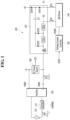
- FIG. 1 is a block diagram of a lighting apparatus 100 according to an exemplary embodiment.
- the lighting apparatus 100 may be connected to an AC power source 110 and receive an AC voltage Vac, and may include a dimmer 115, a rectifier 120, an LED circuit 130, an LED driver 140, a driving current controller 150, and a DC power source 160.
- the dimmer 115 may receive the AC voltage Vac from the AC power source 110, modulate the AC voltage Vac to have a dimming level according to a user's selection, and output the modulated AC voltage.
- the dimmer 115 may include a triac dimmer, which may cut the phase of the AC voltage Vac based on a triac, a pulse-width dimmer, which may modulate the pulse-width of the AC voltage Vac, or etc.
- the inventive concepts are not limited to a particular type of the dimmer.
- the dimmer 115 may output a modulated AC voltage by cutting the phase of the AC voltage Vac based on a dimming level selected by a user. In this case, control over a triac trigger current may be required.
- the lighting apparatus 100 may further include a bleeder circuit connected between the dimmer 115 and the rectifier 120.
- the bleeder circuit may include a capacitor and a resistor.
- the dimmer 115 is shown as a component of the lighting apparatus 100.
- the inventive concepts are not limited thereto.
- the dimmer 115 may be disposed outside the lighting apparatus 100 and be electrically connected with the lighting apparatus 100 in some exemplary embodiments.
- the rectifier 120 may rectify the AC voltage modulated by the dimmer 115 and output a rectified voltage Vrct through a first power node VPND and a second power node VNND.
- the second power node VNND may be a ground node.
- the rectified voltage Vrct is output to the LED circuit 130 and the DC power source 160.
- the lighting apparatus 100 may further include a surge protection circuit to protect internal components of the lighting apparatus 100 from an overvoltage and/or an overcurrent.
- the surge protection circuit may be connected, for example, between the first and second power nodes VPND and VNND.
- the LED circuit 130 is connected between the first and second power nodes VPND and VNND, and operates in response to the rectified voltage Vrct.
- the LED circuit 130 includes a plurality of stages STG1 and STG2, which include LEDs each emitting light. Each of the stages STG1 and STG2 may selectively emit light depending on the level of the rectified voltage Vrct.
- the stages STG1 and STG2 are connected to the LED driver 140 through first and second driving nodes D1 and D2.
- the current of the first and second driving nodes D1 and D2 may be adjusted by the LED driver 140.
- the brightness of light emitted from each of the LEDs included in the stages STG1 and STG2 may be changed depending on the current. When the current of the first and second driving nodes D1 and D2 are adjusted, the brightness of light emitted from each of the LEDs may be changed.
- the LED circuit 130 includes first and second stages STG1 and STG2.
- the first and second stages STG1 and STG2 may be sequentially connected between the first power node VPND and the second driving node D2, and the output terminal of the first stage STG1 may be connected to the first driving node D1.
- the LED circuit 130 may further include a capacitor CP.
- the capacitor CP may be connected between the output terminal of the first stage STG1 and the first driving node D1.
- the capacitor CP may be charged and discharged depending on the level of the rectified voltage Vrct, and may provide current to the first and second stages STG1 and STG2 when being discharged. In this manner, the first and second stages STG1 and STG2 may emit light even when the level of the rectified voltage Vrct becomes lower than corresponding threshold voltages, due to the capacitor CP.
- the LED circuit 130 may further include first to fifth diodes DID1 to DID5 for preventing reverse current.
- the first diode DID1 is connected between the first power node VPND and the first stage STG1, and blocks current flowing from the first stage STG1 to the first power node VPND.
- the second diode DID2 is connected between the output terminal of the first stage STG1 and the capacitor CP, and blocks current flowing from the capacitor CP to the output terminal of the first stage STG1.
- the third diode DID3 is connected between the capacitor CP and the input terminal of the first stage STG1, and blocks current flowing from the input terminal of the first stage STG1 to the capacitor CP.
- the fourth and fifth diodes DID4 and DID5 are connected between the ground node (or the second power node VNND) and the first driving node D1, and a branch node between the fourth and fifth diodes DID4 and DID5 is connected to the capacitor CP.
- the fourth diode DID4 blocks current flowing from the branch node to the ground node
- the fifth diode DID5 blocks current flowing from the first driving node D1 to the branch node.
- the LED driver 140 is connected to the LED circuit 130 through the first and second driving nodes D1 and D2.
- the LED driver 140 provides first and second driving currents DI1 and DI2 to the LED circuit 130 through the first and second driving nodes D1 and D2. As the level of driving current is high, the brightness of light output from a corresponding stage through which the driving current flows may be increased.
- the driving current controller 150 controls the LED driver 140 to adjust the first and second driving currents DI1 and DI2 depending on a dimming signal ADIM indicating a dimming level.
- the dimming signal ADIM may indicate the modulation degree of the rectified voltage Vrct.
- the driving current controller 150 is connected to the LED driver 140 through a current setting node DISND.
- the driving current controller 150 may control the voltage of the current setting node DISND depending on the dimming signal ADIM.
- the LED driver 140 may adjust the levels of the first and second driving currents DI1 and DI2 depending on the voltage of the current setting node DISND. When the voltage of the current setting node DISND increases, the LED driver 140 may increase the levels of the first and second driving currents DI1 and DI2. When the voltage of the current setting node DISND decreases, the LED driver 140 may decrease the levels of the first and second driving currents DI1 and DI2.
- the dimming signal ADIM may be provided through a dimming node ADIMND from the dimmer 115.
- the lighting apparatus 100 may further include a dimming level detector to generate the dimming signal ADIM based on the rectified voltage Vrct.
- the types of dimming signals may be variously modified.
- the dimming level detector may include an RC integrator circuit and output a DC voltage that is based on the rectified voltage Vrct as the dimming signal ADIM.
- the dimming level detector may detect the pulse-width of each period of the rectified voltage Vrct, and may output an analog signal or a digital signal corresponding to a detected pulse-width as the dimming signal ADIM.
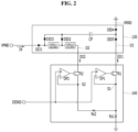
- FIG. 2 is an exemplary circuit diagram of the LED circuit 130 and the LED driver 140 of FIG. 1 .
- the LED driver 140 may include a first transistor TR1, a first comparator OP1, a second transistor TR2, a second comparator OP2, and one or more source resistors Rs1 and Rs2.
- the first transistor TR1 and the first comparator OP1 control the current of the first driving node D1, and the second transistor TR2 and the second comparator OP2 control the current of the second driving node D2.
- the first transistor TR1 is connected between the first driving node D1 and a first source node S1.
- the first comparator OP1 has an output terminal connected to the gate of the first transistor TR1 and an inverting terminal connected to the first source node S1.
- the second transistor TR2 is connected between the second driving node D2 and a second source node S2.
- the second comparator OP2 has an output terminal connected to the gate of the second transistor TR2 and an inverting terminal connected to the second source node S2.
- the non-inverting terminals of the first and second comparators OP1 and OP2 are connected in common to the current setting node DISND.
- the first and second transistors TR1 and TR2 may be NMOS transistors, for example.
- the first transistor TR1 When the voltage of the first source node S1 is lower than the voltage of the current setting node DISND, the first transistor TR1 may be turned on by the output of the first comparator OP1. When the voltage of the first source node S1 becomes higher than the voltage of the current setting node DISND by the rectified voltage Vrct (see FIG. 1 ) provided through the first power node VPND, the first transistor TR1 may be turned off by the output of the first comparator OP1. In this manner, the first transistor TR1 may be repeatedly turned on and off. As such, the voltage of the current setting node DISND may be reflected on the voltage of the first source node S1. Similarly, the voltage of the current setting node DISND may be reflected on the voltage of the second source node S2.
- the first source resistor Rs1 is connected between the first source node S1 and the ground node. Depending on the voltage of the first source node S1 and the resistance of the first source resistor Rs1, the level of the first driving current DI1 may be determined.
- the second source resistor Rs2 is connected between the second source node S2 and the first source node S1. Depending on the voltage of the second source node S2 and the sum of resistance of the first and second source resistors Rs1 and Rs2, the level of the second driving current DI2 may be determined. For example, the level of the second driving current DI2 may be lower than the level of the first driving current DI1.
- the levels of the first and second driving currents DI1 and DI2 may be respectively controlled depending on the voltage of the current setting node DISND.
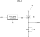
- FIG. 3 is an exemplary block diagram of the driving current controller 150 of FIG. 1 .
- the driving current controller 150 may include a driving current control circuit 151, a voltage regulator 152, and a setting resistor Rset.
- the driving current control circuit 151 may output a driving current control signal DICS depending on the dimming signal ADIM.
- the driving current control signal DICS may be provided as a DC voltage.
- the driving current control circuit 151 may increase the voltage of the driving current control signal DICS as a dimming level when the dimming signal ADIM is high.
- the setting resistor Rset is connected between the current setting node DISND and the ground node.
- a setting capacitor Cset may be connected to the setting resistor Rset in parallel to eliminate or reduce noise in the voltage of the current setting node DISND.
- the voltage regulator 152 regulates the voltage of the current setting node DISND depending on the driving current control signal DICS.
- the voltage regulator 152 may include a variable current source, which generates high current as the voltage of the driving current control signal DICS increases. As high current flows, the voltage of the current setting node DISND may be increased.
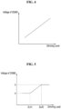
- FIG. 4 is a graph illustrating the voltage of the current setting node DISND biased depending on a dimming level.
- FIG. 5 is a graph illustrating the voltage of the current setting node DISND biased depending on a dimming level.
- the driving current controller 150 may increase the voltage of the current setting node DISND as a dimming level increases.
- the driving current controller 150 may maintain the voltage of the current setting node DISND to a first voltage level "a" when a dimming level is lower than a first reference dimming level DLrf1, may maintain the voltage of the current setting node DISND to a second voltage level "b" higher than the first voltage level "a” when a dimming level is higher than a second reference dimming level DLrf2, and may increase the voltage of the current setting node DISND depending on a dimming level between the first and second voltage levels "a” and "b” when a dimming level is between the first and second reference dimming levels DLrf1 and DLrf2.
- FIG. 6 is a timing diagram illustrating a method for driving the plurality of stages STG1 and STG2 according to an exemplary embodiment.
- the rectified voltage Vrct is received during first to fourth periods PRD1 to PRD4. As the rectified voltage Vrct increases, at a first time t1, it reaches a first voltage Va.
- the first voltage Va may be the sum of the threshold voltages of the first and second stages STG1 and STG2, which are coupled in series.
- input current IN may flow through the first and second stages STG1 and STG2 and the second driving node D2. Accordingly, the first and second stages STG1 and STG2 may emit light.
- the second driving current DI2 of the second driving node D2 may be adjusted to have a first level L1.
- the second voltage Vb may be the sum of the threshold voltage of the first stage STG1 and the voltage across the capacitor CP.
- the input current IN may flow through the first stage STG1, the capacitor CP, and the first driving node D1. Accordingly, the first stage STG1 may emit light. Since the sum of the resistances of the resistors Rs1 and Rs2, which are connected to the second driving node D2 through the second transistor TR2, is higher than the resistance of the resistor Rs1 connected to the first driving node D1 through the first transistor TR1, the second driving current DI2 may be gradually blocked.
- the first driving current DI1 of the first driving node D1 may have a second level L2 higher than the first level L1.
- the input current IN flowing through the first stage STG1, the capacitor CP, and the first driving node D1 is blocked, and may flow through the first and second stages STG1 and STG2 and the second driving node D2.
- the second driving current DI2 may be controlled to have the first level L1.
- the rectified voltage Vrct As the rectified voltage Vrct further decreases, at a fourth time t4, it becomes lower than the first voltage Va.
- the input current IN flowing through the first and second stages STG1 and STG2 and the second driving node D2 is blocked.
- the voltage across the capacitor CP, which is charged, may be higher than the first voltage Va.
- the charges in the capacitor CP may flow through the first and second stages STG1 and STG2 and the second driving node D2. In this manner, the LED circuit 130 may emit light even in a time period when the rectified voltage Vrct becomes lower than the first voltage Va.
- the second driving current DI2 may be controlled to have the first level L1.
- the LED circuit 130 is driven in a manner similar to the first to fourth times t1 to t4. As such, repeated descriptions of the substantially similar operations during the fifth to eighth times t5 to t8 will be omitted to avoid redundancy.
- the rectified voltage Vrct may be modulated.
- a voltage of approximately 0V may be received during a certain time of the third period PRD3, and a voltage higher than 0V may be received during the remaining time.
- a dimming level corresponding to the rectified voltage Vrct of the third period PRD3 is lower than a dimming level corresponding to the rectified voltage Vrct of the first period PRD1 and the second period PRD2.
- the rectified voltage Vrct of the third period PRD3 becomes higher than the second voltage Vb.
- the input current IN may flow through the first stage STG1, the capacitor CP, and the first driving node D1. Accordingly, the first stage STG1 may emit light.
- the charges in the capacitor CP may flow through the first and second stages STG1 and STG2 and the second driving node D2. Since the sum of the resistances of the resistors Rs1 and Rs2 connected to the second driving node D2 is higher than the resistance of the resistor Rs1 connected to the first driving node D1, the second driving current DI2 may be blocked at the ninth time t9.
- the first driving current DI1 of the first driving node D1 is adjusted to have a third level L3 lower than the second level L2.
- the driving current controller 150 adjusts the first and second driving currents DI1 and DI2 depending on the dimming signal ADIM that corresponds to a dimming level. Since the dimming level of the rectified voltage Vrct of the third period PRD3 is lower than the dimming level of the rectified voltage Vrct of the first period PRD1 and the second period PRD2, the first driving current DI1 has the third level L3 lower than the second level L2.
- the rectified voltage Vrct of the third period PRD3 decreases, at a tenth time t10, it becomes lower than the second voltage Vb.
- the input current IN flowing through the first stage STG1, the capacitor CP, and the first driving node D1 is blocked, and may flow through the first and second stages STG1 and STG2 and the second driving node D2. Accordingly, the first and second stages STG1 and STG2 may emit light.
- the second driving current DI2 of the second driving node D2 is adjusted to have a fourth level L4 lower than the first level L1.
- the rectified voltage Vrct of the third period PRD3 As the rectified voltage Vrct of the third period PRD3 further decreases, at an eleventh time t11, it becomes lower than the first voltage Va.
- the input current IN flowing through the first and second stages STG1 and STG2 and the second driving node D2 is blocked.
- the charges in the capacitor CP may flow through the first and second stages STG1 and STG2 and the second driving node D2.
- the second driving current DI2 is controlled to have the fourth level L4.
- the LED circuit 130 is driven in a manner similar to the ninth to eleventh times t9 to t11, and thus, repeated descriptions thereof will be omitted to avoid redundancy.
- FIG. 7 is a circuit diagram of the LED circuit 130 according to the invention.
- FIG. 8 is a graph illustrating the relationship between a forward voltage and forward current for each of a first current path CRP1 and a second current path CRP2.
- the first stage STG1 includes a first current path CRP1 and a second current path CRP2 which are connected in parallel
- the second stage STG2 includes a third current path CRP3 and a fourth current path CRP4 which are connected in parallel.
- the first current path CRP1 of the first stage STG1 includes a first resistor R1 and a first LED LED1 which are connected in series.
- the second current path CRP2 of the first stage STG1 includes a second LED LED2.
- the first and second LEDs LED1 and LED2 may each emit light having different color temperatures.
- the mixed light of the first and second LEDs LED1 and LED2 is output from the first stage STG1.
- the color temperature of the first LED LED1 may be lower than the color temperature of the second LED LED2.
- the third current path CRP3 of the second stage STG2 includes a second resistor R2 and a third LED LED3 which are connected in series.
- the fourth current path CRP4 of the second stage STG2 includes a fourth LED LED4.
- the third LED LED3 may emit light having substantially the same color temperature as the first LED LED1.
- the fourth LED LED4 may emit light having substantially the same color temperature as the second LED LED2.
- the second stage STG2 may be have substantially the same configuration as the first stage STG1.
- a resistor connected in series to an LED reduces the slope (or proportional constant) of forward current with respect to a forward voltage. For example, as the resistance of a resistor serially connected to an LED increases, the slope of forward current with respect to a forward voltage will be decreased. As such, the slope of forward current with respect to a forward voltage in the first current path CRP1 will be lower than that of the second current path CRP2.
- a first voltage-current curve IV1 is a graph showing the relationship between the forward voltage and the forward current of the first current path CRP1
- a second voltage-current curve IV2 is a graph showing the relationship between the forward voltage and the forward current of the second current path CRP2 according to an exemplary embodiment.
- the second threshold voltage Vth2 may be considered as the threshold voltage of the second LED LED2, which is included in the second current path CRP2.
- the first threshold voltage Vth1 may be lower than the second threshold voltage Vth2.
- the first and second LEDs LED1 and LED2 may be configured such that the first threshold voltage Vth1 is lower than the second threshold voltage Vth2.
- the first voltage-current curve IV1 will have a slope lower than the second voltage-current curve IV2. Accordingly, when driving current supplied to the first stage STG1 changes, the ratio of currents distributed to the first and second current paths CRP1 and CRP2 will be changed.
- the first current I1 may flow through the first current path CRP1, as a relatively large amount of driving current is provided to the first stage STG1 by the driving current controller 150.
- the driving current controller 150 adjusts driving current (see DI1 or DI2 of FIG. 1 ) depending on the dimming signal ADIM.
- the first voltage-current curve IV1 the voltage across the first current path CRP1 is a first voltage V1.
- the second current path CRP2 is connected in parallel to the first current path CRP1, the voltage across the second current path CRP2 is also the first voltage V1.
- second current I2 may flow through the second current path CRP2.
- the second current I2 is higher than the first current I1.
- the third current I3 lower than the first current I1 may flow through the first current path CRP1, as the driving current provided to the first stage STG1 decreases.
- the voltage across the first current path CRP1 is a second voltage V2.
- the voltage across the second current path CRP2 is also the second voltage V2.
- fourth current I4 may flow through the second current path CRP2.
- the fourth current I4 is lower than the third current I3.
- the fifth current I5 lower than the third current I3 may flow through the first current path CRP1, as the driving current provided to the first stage STG1 further decreases.
- the voltage across the first current path CRP1 is a third voltage V3.
- the third voltage V3 is lower than the second threshold voltage Vth2. Accordingly, current does not flow through the second current path CRP2, and therefore, the second current path CRP2 does not emit light.
- the first threshold voltage Vth1 may be lower than the second threshold voltage Vth2 so as to provide a dimming level, which causes only the first current path CRP1 having a first color temperature to emit light and while the second current path CRP2 having a second color temperature does not emit light.
- the rate of current flowing through the first current path CRP1 may be increased, and the rate of current flowing through the second current path CRP2 may be decreased.
- the driving current provided to the first stage STG1 changes, the color temperature of the mixed light outputted from the first stage STG1 may be changed.
- the driving current provided to the second stage STG2 changes, the color temperature of the mixed light outputted from the second stage STG2 may be changed. Accordingly, in the lighting apparatus 100 according to an exemplary embodiment, adjusting the driving currents DI1 and DI2 provided to the stages STG1 and STG2 depending on a dimming level can adjust the color temperature of the mixed light outputted from the LED circuit 130.
- the color temperature of the first LED LED1 may be lower than the color temperature of the second LED LED2.
- the color temperature of the mixed light outputted from the first stage STG1 may be decreased.
- the color temperature of the mixed light output from the first stage STG1 may be decreased.
- the lighting apparatus 100 may provide an effect similar to that in incandescent bulb, such as darkening an incandescent bulb decreases the color temperature of light emitted from a filament.
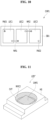
- FIG. 9 is a perspective view of one of the first and third LEDs LED1 and LED3 of FIG. 7 according to an example not part of the subject-matter of the claims.
- the LED LED' may include a housing HS, an LED chip CHP1 mounted in the housing HS, and a wavelength conversion layer WVC1 covering the LED chip CHP1.
- the housing HS may be formed by injection-molding a plastic resin, for example.
- the housing HS may be formed to support lead terminals connected with the LED chip CHP1, by injection molding.
- the housing HS may have a cavity CVT, in which the LED chip CHP1 is mounted.
- the LED chip CHP1 is disposed in the cavity CVT.
- the LED chip CHP1 may include a plurality of light-emitting cells. This will be described in detail later with reference to FIG. 10 .
- the wavelength conversion layer WVC1 covers the LED chip CHP1.
- the wavelength conversion layer WVC1 may be formed by filling the cavity CVT with a molding resin including a fluorescent material after the LED chip CHP1 is mounted in the cavity CVT.
- the LED chip CHP1 including a fluorescent material coating layer as the wavelength conversion layer WVC1 may be mounted in the housing HS. In this case, the LED chip CHP1 may be molded by a transparent resin.
- an optical member may be additionally disposed on the wavelength conversion layer WVC1.
- the wavelength conversion layer WVC1 may convert the wavelength of light emitted from the LED chip CHP1 to generate white light.
- the color temperature of light output from the LED LED' may be determined by the wavelength conversion layer WVC1.
- the plurality of light-emitting cells in the LED chip CHP1 may share the one wavelength conversion layer WVC1. In this manner, a processing error from forming separate wavelength conversion layers for each light emitting cell may be avoided, such that light of a desired color temperature may be emitted from the LED chip CHP1. Accordingly, the LED circuit 130 according to an exemplary embodiment may be capable of precisely adjusting a color temperature to a target color temperature depending on a dimming level.
- FIG. 10 is a top view of the LED chip CHP1 of FIG. 9 according to an example not part of the subject-matter of the claims.
- the LED chip CHP1 may include a substrate SB1, a plurality of light-emitting cells LEC1 to LEC3 disposed on the substrate SB1, wires WR1 and WR2, and two pads PAD1 and PAD2 for connecting the light-emitting cells LEC1 to LEC3 to an external component, such as lead terminals.
- Each of the light-emitting cells LEC1 to LEC3 may include gallium nitride-based material and emit ultraviolet or blue light.
- the plurality of light-emitting cells LEC1 to LEC3 may be connected in series by the wires WR1 and WR2.
- the wires WR1 and WR2 may be replaced with various components capable of electrically connecting the plurality of light-emitting cells LEC1 to LEC3.
- the LED chip CHP1 may include conductive layers, which may be formed through deposition and patterning, and the plurality of light-emitting cells LEC1 to LEC3 may be electrically connected to each other through the conductive layers.
- the threshold voltages of the respective light-emitting cells LEC1 to LEC3 may be substantially the same. In this case, as the number of serially connected light-emitting cells LEC1 to LEC3 in the LED chip CHP1 increases, the threshold voltage of the LED chip CHP1 may be increased.
- FIG. 10 exemplarily illustrates that the LED chip CHP1 includes three light-emitting cells LEC1 to LEC3. However, the inventive concepts are not limited to a particular number of light-emitting cells in the LED chip CHP1.
- FIG. 11 is a perspective view of one of the second and fourth LEDs LED2 and LED4 of FIG. 7 according to an example not part of the subject-matter of the claims.
- the LED LED may include a housing HS, an LED chip CHP2 mounted in the housing HS, and a wavelength conversion layer WVC2 covering the LED chip CHP2.
- the LED chip CHP2 may be disposed in a cavity CVT of the housing HS.
- the LED chip CHP2 includes a plurality of light-emitting cells.
- the LED chip CHP2 includes a larger number of light-emitting cells than the LED chip CHP1 of FIG. 9 . This will be described in detail later with reference to FIG. 12 .
- the wavelength conversion layer WVC2 may convert the wavelength of light emitted from the LED chip CHP2 to generate white light.
- the color temperature of the white light converted by the wavelength conversion layer WVC2 may be higher than that of the wavelength conversion layer WVC1 of FIG. 9 .
- Materials, such as a fluorescent material, of the wavelength conversion layer WVC2 may be appropriately selected to have a desired color temperature.
- the wavelength conversion layer WVC2 may cover the plurality of light-emitting cells in common, to reduce or avoid a processing error described above and to emit light of a desired color temperature. Accordingly, the LED circuit 130 may be capable of precisely adjusting a color temperature to a target color temperature depending on a dimming level.
- FIG. 12 is a top view of the LED chip CHP2 of FIG. 11 according to an example not part of the subject-matter of the claims.
- the LED chip CHP2 may include a substrate SB2, a plurality of light-emitting cells LEC1 to LECn (n is an integer greater than 3) disposed on the substrate SB2, wires for connecting the plurality of light-emitting cells LEC1 to LECn one to another, and two pads PAD1 and PAD2 for connecting the plurality of light-emitting cells LEC1 to LECn to an external component.
- the plurality of light-emitting cells LEC1 to LECn may be connected in series through the wires.
- the wires may be replaced with various components capable of electrically connecting the plurality of light-emitting cells LEC1 to LECn.
- the number of the light-emitting cells LEC1 to LECn included in the LED chip CHP2 is greater than the number of the light-emitting cells LEC1 to LEC3 of the LED chip CHP1 of FIG. 10 .
- the threshold voltage (see Vth2 of FIG. 8 ) of the LED chip CHP2 may be higher than the threshold voltage (see Vth1 of FIG. 8 ) of the LED chip CHP1 of FIG. 10 .
- each LED may include an LED chip having a plurality of light-emitting cells therein and a wavelength conversion layer covering the light-emitting cells in common, and accordingly, may have a reduced processing error and emit light of a desired color temperature. Accordingly, it is possible to provide the LED circuit 130 capable of precisely adjusting a color temperature to a target color temperature depending on a dimming level. Moreover, by adjusting the number of light-emitting cells included in the LED, the threshold voltage of the LED may be efficiently adjusted.
- FIG. 13 is a block diagram of a lighting apparatus 200 according to another example not part of the subject-matter of the claims.
- the lighting apparatus 200 may be connected to an AC power source 210 and receive an AC voltage Vac, and may include a dimmer 215, a rectifier 220, an LED circuit 230, an LED driver 240, a driving current controller 250, and a DC power source 260.
- the dimmer 215, the rectifier 220, the driving current controller 250, and the DC power source 260 are substantially the same as the dimmer 115, the rectifier 120, the driving current controller 150, and the DC power source 160 described above with reference to FIG. 1 . As such, repeated descriptions of the substantially the same elements will be omitted to avoid redundancy.
- the LED circuit 230 may include a plurality of stages STG1 to STG4, which are configured to selectively emit light in response to the level of a rectified voltage Vrct.
- the number of the plurality of stages STG1 to STG4, the connection relationship among the plurality of stages STG1 to STG4, and the connection relationship between the plurality of stages STG1 to STG4 and the LED driver 240 may be changed variously.
- the LED circuit 230 is shown as including four stages STG1 to STG4.
- the first to fourth stages STG1 to STG4 may be sequentially connected through first to fourth driving nodes D1 to D4, and may be connected to the LED driver 240 through the first to fourth driving nodes D1 to D4.
- Each stage is configured in substantially the same manner as the stage described above with reference to FIG. 7 .
- the LED driver 240 is connected to the LED circuit 230 through the first to fourth driving nodes D1 to D4, and may control the driving currents of the first to fourth driving nodes D1 to D4 under the control of the driving current controller 250.
Landscapes
- Physics & Mathematics (AREA)
- Nonlinear Science (AREA)
- Circuit Arrangement For Electric Light Sources In General (AREA)
Claims (4)
- Appareil d'éclairage comprenant
un circuit LED (130 ; 230) comprenant plusieurs étages (STG1, STG2, STG3, STG4) connectés en série et configurés pour recevoir une tension redressée modulée, chacun des étages (STG1, STG2, STG3, STG4) comprenant :un premier chemin comprenant une première résistance (R1 ; R2) et une première LED (LED1, LED3 ; LED') connectée en série ; etun second chemin connecté au premier chemin en parallèle et comprenant une seconde LED (LED2, LED4 ; LED") configurée pour émettre une lumière ayant une température de couleur différente de celle émise par la première LED (LED1, LED3 ; LED') ; etun contrôleur de courant de commande (150 ; 250) configuré pour ajuster une intensité de lumière émise par le circuit LED (130 ; 230) en ajustant les courants appliqués aux noeuds de commande (D1, D2, D3, D4) connectés aux étages respectifs (STG1, STG2, STG3, STG4), en fonction d'un signal de gradation associé à un niveau de gradation de la tension redressée modulée,caractérisé en ce quela deuxième DEL (DEL2, DEL4 ; DEL") a un plus grand nombre de cellules émettrices de lumière que la première DEL (DEL1, DEL3 ; DEL'). - Appareil d'éclairage selon la revendication 1, dans lequel la tension de seuil des cellules émettrices de lumière de la première et de la deuxième DEL (DEL1, DEL3 ; DEL' ; DEL2, DEL4 ; DEL") est la même l'une que l'autre.
- Appareil d'éclairage selon la revendication 1, dans lequel les cellules émettrices de lumière (CHP1, CHP2) de chacune des première et deuxième DEL (LED1, LED3 ; LED' ; LED2, LED4 ; LED") sont connectées en série l'une à l'autre et sont couvertes par une couche de conversion de longueur d'onde (WVC1, WVC2).
- L'appareil d'éclairage selon la revendication 1, comprenant en outre un pilote de LED connecté (140 ; 240) entre le circuit de LED (130 ; 230) et le contrôleur de courant de commande (150 ; 250), le pilote de LED comprenant des comparateurs connectés aux étages (STG1, STG2, STG3, STG4), respectivement.
Applications Claiming Priority (1)
| Application Number | Priority Date | Filing Date | Title |
|---|---|---|---|
| KR1020180037269A KR102420542B1 (ko) | 2018-03-30 | 2018-03-30 | 발광 다이오드들을 포함하는 조명 장치 |
Publications (2)
| Publication Number | Publication Date |
|---|---|
| EP3547802A1 EP3547802A1 (fr) | 2019-10-02 |
| EP3547802B1 true EP3547802B1 (fr) | 2024-01-31 |
Family
ID=66001011
Family Applications (1)
| Application Number | Title | Priority Date | Filing Date |
|---|---|---|---|
| EP19165826.9A Active EP3547802B1 (fr) | 2018-03-30 | 2019-03-28 | Appareil d'éclairage comprenant des diodes électroluminescentes |
Country Status (4)
| Country | Link |
|---|---|
| US (1) | US10757781B2 (fr) |
| EP (1) | EP3547802B1 (fr) |
| KR (1) | KR102420542B1 (fr) |
| CN (1) | CN110324932B (fr) |
Families Citing this family (1)
| Publication number | Priority date | Publication date | Assignee | Title |
|---|---|---|---|---|
| US10791597B2 (en) * | 2017-08-09 | 2020-09-29 | Seoul Semiconductor Co., Ltd. | LED lighting apparatus capable of color temperature control |
Family Cites Families (12)
| Publication number | Priority date | Publication date | Assignee | Title |
|---|---|---|---|---|
| US8120277B2 (en) * | 2008-06-04 | 2012-02-21 | Boca Flasher, Inc. | Hybrid-control current driver for dimming and color mixing in display and illumination systems |
| US8476837B2 (en) * | 2010-07-02 | 2013-07-02 | 3M Innovative Properties Company | Transistor ladder network for driving a light emitting diode series string |
| SE1000801A2 (sv) * | 2010-07-29 | 2012-04-30 | Andreas Vinnberg | LED lampa |
| KR20140130666A (ko) * | 2011-12-16 | 2014-11-11 | 어드밴스드 라이팅 테크놀러지, 인크. | 고역률 내구성 저비용 led 램프 개조형 시스템 및 방법 |
| RU2660801C2 (ru) * | 2013-05-03 | 2018-07-10 | Филипс Лайтинг Холдинг Б.В. | Светодиодная осветительная цепь |
| CN105474755B (zh) * | 2013-07-03 | 2018-07-17 | 万斯创新公司 | 针对可调光ac led照明的光谱偏移控制 |
| CN203788515U (zh) * | 2014-03-11 | 2014-08-20 | 东莞嘉盛照明科技有限公司 | 一种调节发光二极管色温和光通量的电路 |
| JP6328227B2 (ja) * | 2014-03-20 | 2018-05-23 | 東芝マテリアル株式会社 | 発光装置およびled電球 |
| TWM485583U (zh) * | 2014-05-16 | 2014-09-01 | Unity Opto Technology Co Ltd | 純電阻式調光電路 |
| CN108240613B (zh) * | 2016-12-23 | 2021-10-26 | 首尔半导体股份有限公司 | Led驱动用系统级封装及含其的led照明装置 |
| CN106658871A (zh) * | 2017-02-28 | 2017-05-10 | 漳州立达信光电子科技有限公司 | 一种可调色温的发光二极管电路 |
| KR102147564B1 (ko) * | 2017-10-13 | 2020-08-24 | 주식회사 루멘스 | 조명 장치 |
-
2018
- 2018-03-30 KR KR1020180037269A patent/KR102420542B1/ko active IP Right Grant
-
2019
- 2019-03-28 EP EP19165826.9A patent/EP3547802B1/fr active Active
- 2019-03-29 US US16/368,875 patent/US10757781B2/en active Active
- 2019-03-29 CN CN201910248876.0A patent/CN110324932B/zh active Active
Also Published As
| Publication number | Publication date |
|---|---|
| KR20190114486A (ko) | 2019-10-10 |
| EP3547802A1 (fr) | 2019-10-02 |
| CN110324932B (zh) | 2022-01-11 |
| KR102420542B1 (ko) | 2022-07-13 |
| US10757781B2 (en) | 2020-08-25 |
| CN110324932A (zh) | 2019-10-11 |
| US20190306942A1 (en) | 2019-10-03 |
Similar Documents
| Publication | Publication Date | Title |
|---|---|---|
| US9713211B2 (en) | Solid state lighting apparatus with controllable bypass circuits and methods of operation thereof | |
| US10264637B2 (en) | Solid state lighting apparatus with compensation bypass circuits and methods of operation thereof | |
| US10342082B2 (en) | Linear lighting with distributed power conversion and reduced flicker | |
| US8674610B2 (en) | Lighting apparatus and circuits for lighting apparatus | |
| EP2589268B1 (fr) | Réseau en échelle à transistor permettant de commander une chaîne montée en série de diodes électroluminescentes | |
| WO2013118208A1 (fr) | Circuit électroluminescent, module électroluminescent et dispositif d'éclairage | |
| US20200413514A1 (en) | Dim-to-warm led circuit | |
| EP2863713A2 (fr) | Appareil d'éclairage à DEL à commande CA à intensité réglable | |
| KR20200000468A (ko) | 발광 다이오드 조명 시스템 제어 방법 및 시스템 | |
| CN103891406A (zh) | 利用切相调光器角度与预定黑体辐射函数之间的相关性的电子光源的颜色混合 | |
| US9210767B2 (en) | Lighting apparatus and light emitting diode device thereof | |
| KR102650693B1 (ko) | Led 모듈, led 드라이버, 및 led 조명 장치 | |
| EP3618573B1 (fr) | Module de commande de diode électroluminescente, son procédé de fonctionnement et appareil d'éclairage le comprenant | |
| US10342080B2 (en) | System-in-package for LED driving and LED lighting device including the same | |
| US20200337129A1 (en) | Led lighting apparatus capable of color temperature control | |
| EP3547802B1 (fr) | Appareil d'éclairage comprenant des diodes électroluminescentes | |
| US10149358B1 (en) | Programmable control elements for illumination systems | |
| US10051697B2 (en) | Free voltage LED driving device with high luminous uniformity ratio | |
| US9603218B1 (en) | Controlled color transition | |
| KR101964681B1 (ko) | 고 발광 균제도 프리 볼트 led 구동 장치 | |
| WO2013076480A2 (fr) | Source de lumière del à réglage passif de chromaticité | |
| KR20170086946A (ko) | 동일 발광면 전류 가변 회로 | |
| TWM521267U (zh) | 可變動功率的發光二極體組件封裝結構 |
Legal Events
| Date | Code | Title | Description |
|---|---|---|---|
| PUAI | Public reference made under article 153(3) epc to a published international application that has entered the european phase |
Free format text: ORIGINAL CODE: 0009012 |
|
| STAA | Information on the status of an ep patent application or granted ep patent |
Free format text: STATUS: THE APPLICATION HAS BEEN PUBLISHED |
|
| AK | Designated contracting states |
Kind code of ref document: A1 Designated state(s): AL AT BE BG CH CY CZ DE DK EE ES FI FR GB GR HR HU IE IS IT LI LT LU LV MC MK MT NL NO PL PT RO RS SE SI SK SM TR |
|
| AX | Request for extension of the european patent |
Extension state: BA ME |
|
| STAA | Information on the status of an ep patent application or granted ep patent |
Free format text: STATUS: REQUEST FOR EXAMINATION WAS MADE |
|
| 17P | Request for examination filed |
Effective date: 20191204 |
|
| RBV | Designated contracting states (corrected) |
Designated state(s): AL AT BE BG CH CY CZ DE DK EE ES FI FR GB GR HR HU IE IS IT LI LT LU LV MC MK MT NL NO PL PT RO RS SE SI SK SM TR |
|
| STAA | Information on the status of an ep patent application or granted ep patent |
Free format text: STATUS: EXAMINATION IS IN PROGRESS |
|
| 17Q | First examination report despatched |
Effective date: 20200330 |
|
| REG | Reference to a national code |
Ref country code: DE Ref legal event code: R079 Ref document number: 602019045878 Country of ref document: DE Free format text: PREVIOUS MAIN CLASS: H05B0033080000 Ipc: H05B0045200000 Ref country code: DE Ref legal event code: R079 Free format text: PREVIOUS MAIN CLASS: H05B0033080000 |
|
| RIC1 | Information provided on ipc code assigned before grant |
Ipc: H05B 45/3577 20200101ALI20201123BHEP Ipc: H05B 45/20 20200101AFI20201123BHEP |
|
| STAA | Information on the status of an ep patent application or granted ep patent |
Free format text: STATUS: EXAMINATION IS IN PROGRESS |
|
| GRAP | Despatch of communication of intention to grant a patent |
Free format text: ORIGINAL CODE: EPIDOSNIGR1 |
|
| STAA | Information on the status of an ep patent application or granted ep patent |
Free format text: STATUS: GRANT OF PATENT IS INTENDED |
|
| INTG | Intention to grant announced |
Effective date: 20230821 |
|
| GRAS | Grant fee paid |
Free format text: ORIGINAL CODE: EPIDOSNIGR3 |
|
| GRAA | (expected) grant |
Free format text: ORIGINAL CODE: 0009210 |
|
| STAA | Information on the status of an ep patent application or granted ep patent |
Free format text: STATUS: THE PATENT HAS BEEN GRANTED |
|
| AK | Designated contracting states |
Kind code of ref document: B1 Designated state(s): AL AT BE BG CH CY CZ DE DK EE ES FI FR GB GR HR HU IE IS IT LI LT LU LV MC MK MT NL NO PL PT RO RS SE SI SK SM TR |
|
| REG | Reference to a national code |
Ref country code: GB Ref legal event code: FG4D Ref country code: CH Ref legal event code: EP |
|
| REG | Reference to a national code |
Ref country code: DE Ref legal event code: R096 Ref document number: 602019045878 Country of ref document: DE |
|
| REG | Reference to a national code |
Ref country code: IE Ref legal event code: FG4D |
|
| U01 | Request for unitary effect filed |
Effective date: 20240221 |
|
| U07 | Unitary effect registered |
Designated state(s): AT BE BG DE DK EE FI FR IT LT LU LV MT NL PT SE SI Effective date: 20240301 |
|
| U20 | Renewal fee paid [unitary effect] |
Year of fee payment: 6 Effective date: 20240314 |