EP3547026B1 - Procédé de fabrication d'un tampon métallique pour le gaufrage d'une nano et/ou microstructure sur un dispositif métallique ainsi que ses utilisations et dispositifs fabriqués à partir de celui-ci - Google Patents
Procédé de fabrication d'un tampon métallique pour le gaufrage d'une nano et/ou microstructure sur un dispositif métallique ainsi que ses utilisations et dispositifs fabriqués à partir de celui-ci Download PDFInfo
- Publication number
- EP3547026B1 EP3547026B1 EP18164630.8A EP18164630A EP3547026B1 EP 3547026 B1 EP3547026 B1 EP 3547026B1 EP 18164630 A EP18164630 A EP 18164630A EP 3547026 B1 EP3547026 B1 EP 3547026B1
- Authority
- EP
- European Patent Office
- Prior art keywords
- metal
- stamp
- grating
- nano
- microstructure
- Prior art date
- Legal status (The legal status is an assumption and is not a legal conclusion. Google has not performed a legal analysis and makes no representation as to the accuracy of the status listed.)
- Active
Links
- 229910052751 metal Inorganic materials 0.000 title claims description 162
- 239000002184 metal Substances 0.000 title claims description 162
- 238000004049 embossing Methods 0.000 title claims description 54
- 238000004519 manufacturing process Methods 0.000 title claims description 6
- 239000000463 material Substances 0.000 claims description 101
- 238000000034 method Methods 0.000 claims description 70
- 230000003287 optical effect Effects 0.000 claims description 42
- PXHVJJICTQNCMI-UHFFFAOYSA-N Nickel Chemical compound [Ni] PXHVJJICTQNCMI-UHFFFAOYSA-N 0.000 claims description 32
- 238000005530 etching Methods 0.000 claims description 29
- 229910000831 Steel Inorganic materials 0.000 claims description 23
- 239000010959 steel Substances 0.000 claims description 23
- RTAQQCXQSZGOHL-UHFFFAOYSA-N Titanium Chemical compound [Ti] RTAQQCXQSZGOHL-UHFFFAOYSA-N 0.000 claims description 18
- 239000010936 titanium Substances 0.000 claims description 18
- 229910052719 titanium Inorganic materials 0.000 claims description 18
- 229910052759 nickel Inorganic materials 0.000 claims description 16
- 238000000576 coating method Methods 0.000 claims description 14
- 239000011248 coating agent Substances 0.000 claims description 13
- 238000010884 ion-beam technique Methods 0.000 claims description 13
- 229910000760 Hardened steel Inorganic materials 0.000 claims description 12
- 239000000203 mixture Substances 0.000 claims description 12
- 229920000728 polyester Polymers 0.000 claims description 10
- 229910001069 Ti alloy Inorganic materials 0.000 claims description 9
- 229920000642 polymer Polymers 0.000 claims description 8
- JOYRKODLDBILNP-UHFFFAOYSA-N Ethyl urethane Chemical compound CCOC(N)=O JOYRKODLDBILNP-UHFFFAOYSA-N 0.000 claims description 7
- 239000004952 Polyamide Substances 0.000 claims description 7
- VYPSYNLAJGMNEJ-UHFFFAOYSA-N Silicium dioxide Chemical compound O=[Si]=O VYPSYNLAJGMNEJ-UHFFFAOYSA-N 0.000 claims description 7
- 238000005266 casting Methods 0.000 claims description 7
- 238000005498 polishing Methods 0.000 claims description 7
- 229920002647 polyamide Polymers 0.000 claims description 7
- 239000000126 substance Substances 0.000 claims description 7
- 239000004642 Polyimide Substances 0.000 claims description 6
- MCMNRKCIXSYSNV-UHFFFAOYSA-N Zirconium dioxide Chemical compound O=[Zr]=O MCMNRKCIXSYSNV-UHFFFAOYSA-N 0.000 claims description 6
- 238000001312 dry etching Methods 0.000 claims description 6
- 229920003229 poly(methyl methacrylate) Polymers 0.000 claims description 6
- -1 polyethylene Polymers 0.000 claims description 6
- 229920001721 polyimide Polymers 0.000 claims description 6
- 239000004926 polymethyl methacrylate Substances 0.000 claims description 6
- NIXOWILDQLNWCW-UHFFFAOYSA-M Acrylate Chemical compound [O-]C(=O)C=C NIXOWILDQLNWCW-UHFFFAOYSA-M 0.000 claims description 5
- 239000004593 Epoxy Substances 0.000 claims description 5
- QVGXLLKOCUKJST-UHFFFAOYSA-N atomic oxygen Chemical compound [O] QVGXLLKOCUKJST-UHFFFAOYSA-N 0.000 claims description 5
- 229920001971 elastomer Polymers 0.000 claims description 5
- 239000000806 elastomer Substances 0.000 claims description 5
- 239000005350 fused silica glass Substances 0.000 claims description 5
- 239000001301 oxygen Substances 0.000 claims description 5
- 229910052760 oxygen Inorganic materials 0.000 claims description 5
- 238000003825 pressing Methods 0.000 claims description 5
- 230000003746 surface roughness Effects 0.000 claims description 5
- UONOETXJSWQNOL-UHFFFAOYSA-N tungsten carbide Chemical compound [W+]#[C-] UONOETXJSWQNOL-UHFFFAOYSA-N 0.000 claims description 5
- XKRFYHLGVUSROY-UHFFFAOYSA-N Argon Chemical compound [Ar] XKRFYHLGVUSROY-UHFFFAOYSA-N 0.000 claims description 4
- CERQOIWHTDAKMF-UHFFFAOYSA-M Methacrylate Chemical compound CC(=C)C([O-])=O CERQOIWHTDAKMF-UHFFFAOYSA-M 0.000 claims description 4
- 239000011888 foil Substances 0.000 claims description 4
- 238000003801 milling Methods 0.000 claims description 4
- 229920002120 photoresistant polymer Polymers 0.000 claims description 4
- 239000004417 polycarbonate Substances 0.000 claims description 4
- 229920000515 polycarbonate Polymers 0.000 claims description 4
- 230000010076 replication Effects 0.000 claims description 4
- 239000004743 Polypropylene Substances 0.000 claims description 3
- 229910052581 Si3N4 Inorganic materials 0.000 claims description 3
- 229910052782 aluminium Inorganic materials 0.000 claims description 3
- XAGFODPZIPBFFR-UHFFFAOYSA-N aluminium Chemical compound [Al] XAGFODPZIPBFFR-UHFFFAOYSA-N 0.000 claims description 3
- 238000006243 chemical reaction Methods 0.000 claims description 3
- 239000004205 dimethyl polysiloxane Substances 0.000 claims description 3
- 235000013870 dimethyl polysiloxane Nutrition 0.000 claims description 3
- 229920000840 ethylene tetrafluoroethylene copolymer Polymers 0.000 claims description 3
- 229920002313 fluoropolymer Polymers 0.000 claims description 3
- 239000004811 fluoropolymer Substances 0.000 claims description 3
- 239000011521 glass Substances 0.000 claims description 3
- CXQXSVUQTKDNFP-UHFFFAOYSA-N octamethyltrisiloxane Chemical compound C[Si](C)(C)O[Si](C)(C)O[Si](C)(C)C CXQXSVUQTKDNFP-UHFFFAOYSA-N 0.000 claims description 3
- 238000004987 plasma desorption mass spectroscopy Methods 0.000 claims description 3
- 239000004033 plastic Substances 0.000 claims description 3
- 229920003023 plastic Polymers 0.000 claims description 3
- 229920000435 poly(dimethylsiloxane) Polymers 0.000 claims description 3
- 229920000058 polyacrylate Polymers 0.000 claims description 3
- 229920001155 polypropylene Polymers 0.000 claims description 3
- 239000004810 polytetrafluoroethylene Substances 0.000 claims description 3
- 229920001343 polytetrafluoroethylene Polymers 0.000 claims description 3
- 238000004528 spin coating Methods 0.000 claims description 3
- 238000005507 spraying Methods 0.000 claims description 3
- 239000010935 stainless steel Substances 0.000 claims description 3
- 229910001220 stainless steel Inorganic materials 0.000 claims description 3
- HCHKCACWOHOZIP-UHFFFAOYSA-N Zinc Chemical compound [Zn] HCHKCACWOHOZIP-UHFFFAOYSA-N 0.000 claims description 2
- 239000004411 aluminium Substances 0.000 claims description 2
- 229910052786 argon Inorganic materials 0.000 claims description 2
- 239000007789 gas Substances 0.000 claims description 2
- 229910052758 niobium Inorganic materials 0.000 claims description 2
- 239000010955 niobium Substances 0.000 claims description 2
- GUCVJGMIXFAOAE-UHFFFAOYSA-N niobium atom Chemical compound [Nb] GUCVJGMIXFAOAE-UHFFFAOYSA-N 0.000 claims description 2
- 239000005020 polyethylene terephthalate Substances 0.000 claims description 2
- 229920000139 polyethylene terephthalate Polymers 0.000 claims description 2
- 230000003362 replicative effect Effects 0.000 claims description 2
- 238000000992 sputter etching Methods 0.000 claims description 2
- 229910052715 tantalum Inorganic materials 0.000 claims description 2
- GUVRBAGPIYLISA-UHFFFAOYSA-N tantalum atom Chemical compound [Ta] GUVRBAGPIYLISA-UHFFFAOYSA-N 0.000 claims description 2
- 238000009281 ultraviolet germicidal irradiation Methods 0.000 claims description 2
- 229910052720 vanadium Inorganic materials 0.000 claims description 2
- 229910052725 zinc Inorganic materials 0.000 claims description 2
- 239000011701 zinc Substances 0.000 claims description 2
- 229920002845 Poly(methacrylic acid) Polymers 0.000 claims 4
- 229920001577 copolymer Polymers 0.000 claims 3
- 239000004698 Polyethylene Substances 0.000 claims 1
- QOSMNYMQXIVWKY-UHFFFAOYSA-N Propyl levulinate Chemical compound CCCOC(=O)CCC(C)=O QOSMNYMQXIVWKY-UHFFFAOYSA-N 0.000 claims 1
- 125000001931 aliphatic group Chemical group 0.000 claims 1
- 125000004494 ethyl ester group Chemical group 0.000 claims 1
- 229920000573 polyethylene Polymers 0.000 claims 1
- 229920006012 semi-aromatic polyamide Polymers 0.000 claims 1
- 239000002210 silicon-based material Substances 0.000 claims 1
- LEONUFNNVUYDNQ-UHFFFAOYSA-N vanadium atom Chemical compound [V] LEONUFNNVUYDNQ-UHFFFAOYSA-N 0.000 claims 1
- 239000007943 implant Substances 0.000 description 13
- 238000012546 transfer Methods 0.000 description 8
- 239000002086 nanomaterial Substances 0.000 description 6
- 230000000295 complement effect Effects 0.000 description 5
- 239000004053 dental implant Substances 0.000 description 4
- 239000011368 organic material Substances 0.000 description 4
- 238000001020 plasma etching Methods 0.000 description 4
- 239000002131 composite material Substances 0.000 description 3
- 238000004132 cross linking Methods 0.000 description 3
- 239000013536 elastomeric material Substances 0.000 description 3
- 238000005516 engineering process Methods 0.000 description 3
- 238000007373 indentation Methods 0.000 description 3
- 150000002739 metals Chemical class 0.000 description 3
- 230000000737 periodic effect Effects 0.000 description 3
- 238000012876 topography Methods 0.000 description 3
- XUIMIQQOPSSXEZ-UHFFFAOYSA-N Silicon Chemical compound [Si] XUIMIQQOPSSXEZ-UHFFFAOYSA-N 0.000 description 2
- 238000011161 development Methods 0.000 description 2
- 239000010432 diamond Substances 0.000 description 2
- 229910003460 diamond Inorganic materials 0.000 description 2
- 238000009713 electroplating Methods 0.000 description 2
- 238000010438 heat treatment Methods 0.000 description 2
- 238000010330 laser marking Methods 0.000 description 2
- 238000005259 measurement Methods 0.000 description 2
- NFFIWVVINABMKP-UHFFFAOYSA-N methylidynetantalum Chemical compound [Ta]#C NFFIWVVINABMKP-UHFFFAOYSA-N 0.000 description 2
- 238000001000 micrograph Methods 0.000 description 2
- 238000012986 modification Methods 0.000 description 2
- 230000004048 modification Effects 0.000 description 2
- 238000000465 moulding Methods 0.000 description 2
- 238000000206 photolithography Methods 0.000 description 2
- 239000002861 polymer material Substances 0.000 description 2
- 229920002635 polyurethane Polymers 0.000 description 2
- 239000004814 polyurethane Substances 0.000 description 2
- 239000010453 quartz Substances 0.000 description 2
- 229910052710 silicon Inorganic materials 0.000 description 2
- 239000010703 silicon Substances 0.000 description 2
- 229910003468 tantalcarbide Inorganic materials 0.000 description 2
- MTPVUVINMAGMJL-UHFFFAOYSA-N trimethyl(1,1,2,2,2-pentafluoroethyl)silane Chemical compound C[Si](C)(C)C(F)(F)C(F)(F)F MTPVUVINMAGMJL-UHFFFAOYSA-N 0.000 description 2
- 238000010146 3D printing Methods 0.000 description 1
- 229910000838 Al alloy Inorganic materials 0.000 description 1
- OKTJSMMVPCPJKN-UHFFFAOYSA-N Carbon Chemical compound [C] OKTJSMMVPCPJKN-UHFFFAOYSA-N 0.000 description 1
- VYZAMTAEIAYCRO-UHFFFAOYSA-N Chromium Chemical compound [Cr] VYZAMTAEIAYCRO-UHFFFAOYSA-N 0.000 description 1
- ATJFFYVFTNAWJD-UHFFFAOYSA-N Tin Chemical compound [Sn] ATJFFYVFTNAWJD-UHFFFAOYSA-N 0.000 description 1
- 238000005299 abrasion Methods 0.000 description 1
- 239000002253 acid Substances 0.000 description 1
- 150000007513 acids Chemical class 0.000 description 1
- 239000000853 adhesive Substances 0.000 description 1
- 238000004026 adhesive bonding Methods 0.000 description 1
- 230000001070 adhesive effect Effects 0.000 description 1
- 229910045601 alloy Inorganic materials 0.000 description 1
- 239000000956 alloy Substances 0.000 description 1
- 238000002048 anodisation reaction Methods 0.000 description 1
- 238000013459 approach Methods 0.000 description 1
- 229910052799 carbon Inorganic materials 0.000 description 1
- 238000003486 chemical etching Methods 0.000 description 1
- 239000003795 chemical substances by application Substances 0.000 description 1
- 150000001875 compounds Chemical class 0.000 description 1
- 230000006835 compression Effects 0.000 description 1
- 238000007906 compression Methods 0.000 description 1
- 230000007547 defect Effects 0.000 description 1
- 230000001419 dependent effect Effects 0.000 description 1
- 238000000151 deposition Methods 0.000 description 1
- 230000008021 deposition Effects 0.000 description 1
- 238000013461 design Methods 0.000 description 1
- 230000005489 elastic deformation Effects 0.000 description 1
- 239000003999 initiator Substances 0.000 description 1
- 238000002347 injection Methods 0.000 description 1
- 239000007924 injection Substances 0.000 description 1
- 239000000976 ink Substances 0.000 description 1
- 238000005468 ion implantation Methods 0.000 description 1
- 238000002372 labelling Methods 0.000 description 1
- 238000010030 laminating Methods 0.000 description 1
- 239000007788 liquid Substances 0.000 description 1
- 238000001459 lithography Methods 0.000 description 1
- 238000003913 materials processing Methods 0.000 description 1
- 230000003340 mental effect Effects 0.000 description 1
- 238000004377 microelectronic Methods 0.000 description 1
- 238000010137 moulding (plastic) Methods 0.000 description 1
- 150000004767 nitrides Chemical class 0.000 description 1
- 238000004806 packaging method and process Methods 0.000 description 1
- 239000003973 paint Substances 0.000 description 1
- 239000000049 pigment Substances 0.000 description 1
- 238000007747 plating Methods 0.000 description 1
- 229910052761 rare earth metal Inorganic materials 0.000 description 1
- 239000011347 resin Substances 0.000 description 1
- 229920005989 resin Polymers 0.000 description 1
- 229910052706 scandium Inorganic materials 0.000 description 1
- SIXSYDAISGFNSX-UHFFFAOYSA-N scandium atom Chemical compound [Sc] SIXSYDAISGFNSX-UHFFFAOYSA-N 0.000 description 1
- 239000007779 soft material Substances 0.000 description 1
- 239000007787 solid Substances 0.000 description 1
- 239000000243 solution Substances 0.000 description 1
- 239000002904 solvent Substances 0.000 description 1
- 239000002436 steel type Substances 0.000 description 1
- 239000000758 substrate Substances 0.000 description 1
- 239000004094 surface-active agent Substances 0.000 description 1
- 229910021654 trace metal Inorganic materials 0.000 description 1
- GPPXJZIENCGNKB-UHFFFAOYSA-N vanadium Chemical compound [V]#[V] GPPXJZIENCGNKB-UHFFFAOYSA-N 0.000 description 1
- 230000000007 visual effect Effects 0.000 description 1
Images


Classifications
-
- B—PERFORMING OPERATIONS; TRANSPORTING
- B21—MECHANICAL METAL-WORKING WITHOUT ESSENTIALLY REMOVING MATERIAL; PUNCHING METAL
- B21D—WORKING OR PROCESSING OF SHEET METAL OR METAL TUBES, RODS OR PROFILES WITHOUT ESSENTIALLY REMOVING MATERIAL; PUNCHING METAL
- B21D22/00—Shaping without cutting, by stamping, spinning, or deep-drawing
- B21D22/02—Stamping using rigid devices or tools
-
- G—PHYSICS
- G03—PHOTOGRAPHY; CINEMATOGRAPHY; ANALOGOUS TECHNIQUES USING WAVES OTHER THAN OPTICAL WAVES; ELECTROGRAPHY; HOLOGRAPHY
- G03F—PHOTOMECHANICAL PRODUCTION OF TEXTURED OR PATTERNED SURFACES, e.g. FOR PRINTING, FOR PROCESSING OF SEMICONDUCTOR DEVICES; MATERIALS THEREFOR; ORIGINALS THEREFOR; APPARATUS SPECIALLY ADAPTED THEREFOR
- G03F7/00—Photomechanical, e.g. photolithographic, production of textured or patterned surfaces, e.g. printing surfaces; Materials therefor, e.g. comprising photoresists; Apparatus specially adapted therefor
- G03F7/0002—Lithographic processes using patterning methods other than those involving the exposure to radiation, e.g. by stamping
-
- A—HUMAN NECESSITIES
- A61—MEDICAL OR VETERINARY SCIENCE; HYGIENE
- A61C—DENTISTRY; APPARATUS OR METHODS FOR ORAL OR DENTAL HYGIENE
- A61C8/00—Means to be fixed to the jaw-bone for consolidating natural teeth or for fixing dental prostheses thereon; Dental implants; Implanting tools
- A61C8/0012—Means to be fixed to the jaw-bone for consolidating natural teeth or for fixing dental prostheses thereon; Dental implants; Implanting tools characterised by the material or composition, e.g. ceramics, surface layer, metal alloy
-
- A—HUMAN NECESSITIES
- A61—MEDICAL OR VETERINARY SCIENCE; HYGIENE
- A61C—DENTISTRY; APPARATUS OR METHODS FOR ORAL OR DENTAL HYGIENE
- A61C8/00—Means to be fixed to the jaw-bone for consolidating natural teeth or for fixing dental prostheses thereon; Dental implants; Implanting tools
- A61C8/0018—Means to be fixed to the jaw-bone for consolidating natural teeth or for fixing dental prostheses thereon; Dental implants; Implanting tools characterised by the shape
- A61C8/0037—Details of the shape
-
- B—PERFORMING OPERATIONS; TRANSPORTING
- B21—MECHANICAL METAL-WORKING WITHOUT ESSENTIALLY REMOVING MATERIAL; PUNCHING METAL
- B21D—WORKING OR PROCESSING OF SHEET METAL OR METAL TUBES, RODS OR PROFILES WITHOUT ESSENTIALLY REMOVING MATERIAL; PUNCHING METAL
- B21D37/00—Tools as parts of machines covered by this subclass
- B21D37/20—Making tools by operations not covered by a single other subclass
-
- B—PERFORMING OPERATIONS; TRANSPORTING
- B21—MECHANICAL METAL-WORKING WITHOUT ESSENTIALLY REMOVING MATERIAL; PUNCHING METAL
- B21D—WORKING OR PROCESSING OF SHEET METAL OR METAL TUBES, RODS OR PROFILES WITHOUT ESSENTIALLY REMOVING MATERIAL; PUNCHING METAL
- B21D47/00—Making rigid structural elements or units, e.g. honeycomb structures
- B21D47/005—Making gratings
-
- B—PERFORMING OPERATIONS; TRANSPORTING
- B81—MICROSTRUCTURAL TECHNOLOGY
- B81C—PROCESSES OR APPARATUS SPECIALLY ADAPTED FOR THE MANUFACTURE OR TREATMENT OF MICROSTRUCTURAL DEVICES OR SYSTEMS
- B81C1/00—Manufacture or treatment of devices or systems in or on a substrate
- B81C1/00436—Shaping materials, i.e. techniques for structuring the substrate or the layers on the substrate
- B81C1/00444—Surface micromachining, i.e. structuring layers on the substrate
- B81C1/0046—Surface micromachining, i.e. structuring layers on the substrate using stamping, e.g. imprinting
-
- A—HUMAN NECESSITIES
- A61—MEDICAL OR VETERINARY SCIENCE; HYGIENE
- A61C—DENTISTRY; APPARATUS OR METHODS FOR ORAL OR DENTAL HYGIENE
- A61C8/00—Means to be fixed to the jaw-bone for consolidating natural teeth or for fixing dental prostheses thereon; Dental implants; Implanting tools
- A61C8/0018—Means to be fixed to the jaw-bone for consolidating natural teeth or for fixing dental prostheses thereon; Dental implants; Implanting tools characterised by the shape
- A61C8/0037—Details of the shape
- A61C2008/0046—Textured surface, e.g. roughness, microstructure
-
- B—PERFORMING OPERATIONS; TRANSPORTING
- B21—MECHANICAL METAL-WORKING WITHOUT ESSENTIALLY REMOVING MATERIAL; PUNCHING METAL
- B21D—WORKING OR PROCESSING OF SHEET METAL OR METAL TUBES, RODS OR PROFILES WITHOUT ESSENTIALLY REMOVING MATERIAL; PUNCHING METAL
- B21D37/00—Tools as parts of machines covered by this subclass
- B21D37/01—Selection of materials
Definitions
- the present invention relates to methods for producing a metal stamp for embossing a nano- and/or microstructure on a metal device, to methods of generating an optical diffractive element in the form of a submicron grating on a metal device using such a metal stamp, as well as to devices comprising at least one nano- and/or microstructure which is directly embossed in an exposed metal surface of a load bearing part using such a metal stamp.
- US2005187339A1 is directed to a material for use in imprint lithography that features a composition having a viscosity associated therewith and including a surfactant, a polymerizable component, and an initiator responsive to a stimuli to vary the viscosity in response thereto, with the composition, in a liquid state, having the viscosity being lower than about 100 centipoises, a vapor pressure of less than about 20 Torr, and in a solid cured state a tensile modulus of greater than about 100 MPa, a break stress of greater than about 3 MPa and an elongation at break of greater than about 2%.
- US2017100204A1 relates to a method of marking a surgical instrument with a symbol formed in or on a smooth surface and comprises forming a symbol in or on a smooth surface of the surgical instrument; and forming a plurality of angled surfaces over at least part of the area of the symbol.
- the angled surfaces define a plurality of parallel ridges and grooves in the symbol. The steps of forming the symbol and forming the plurality of angled surfaces take place substantially simultaneously in a single step.
- US2012297856 discloses a method and a process for obtaining a metal stamp from an intermediate polymer stamp comprising the steps of providing a first print layer on top of a first polymer layer, imprinting structures to obtain an intermediate stamp. A conductive layer is provided on top of the structures to obtain a seed layer if the imprinted polymer is a nonconductive, plating metal on top of the intermediate polymer stamp to obtain a metal stamp then separating the intermediate stamp from the metal stamp.
- This invention demonstrates stamp replication in high throughput and at low cost.
- US2010301004 discloses how an electrodeposited Nickel stamp is replicated from a conductive master, e.g. Titanium metallic master instead of a photoresist patterned master.
- the conductive layer is served as a working electrode in the subsequent electrodepositing of the Nickel metal.
- Nickel stamps are obtained by peeling the Nickel metal sheet off the conductive layer of the metallic master. Low adhesion between metallic master and Nickel stamp make it possible to delaminate the Nickel stamp without any defects.
- US2009325107 discloses methods of forming a lens master wafer having aspheric lens shapes.
- a substrate is coated with a polymer material. Isolated sections are formed in the polymer material. The isolated sections are reflowed. The reflowed sections are formed into aspheric lens shapes using a lens stamp.
- US5728324 proposes a method of fabricating a diffractive optical element which includes the steps of: etching a negative of a desired multi-level diffraction pattern onto a molding surface of a quartz master element using photolithography, assembling the master element as a portion of a mold, and injecting a plastic molding composition into the mold and against the molding surface of the master element to injection mold a diffractive optical element, whereby the optical element has the desired diffraction pattern on its surface.
- the diffraction pattern is preferably formed on the quartz master using VLSI photolithography.
- the nanofeatures are imprinted at room temperature using diamond stamps in a single step.
- the imprint properties of the titanium surface can be altered by anodisation, in particular for curved titanium surfaces where a reduced imprint force is preferable to avoid sample deformation and damage.
- the invention solves this problem by providing a method for making a metal stamp tool for embossing an optical security element on any kind of metal device, a metal stamp tool made by this method,
- the device comprises at least one optical security feature comprising diffractive elements made of nano- and/or microstructures, with one or more gratings which are directly embossed in an exposed metal surface in the form of a security and/or identification element.
- Micro structuring is defined as the creation of surface structures which are submicronic in dimensions (i.e. periodicity smaller than 1 ⁇ m, typically in the range of 200-800 nm), in the micron-scale or of a few microns (typically at most 5 ⁇ m or at most 2 ⁇ m) in dimensions.
- the ridge/groove sizes can be submicronic (i.e.
- the depth of the microstructure in the submicron domain while the microstructure periodicity can be larger than one micron, for example less than or 2 ⁇ m.
- the nano- and/or microstructures can comprise or consist of non-periodic nano- and/or microstructures such as Fourier or Fresnel Diffractive Optical Element (DOE), random microstructures, Optically Variable Devices (OVDs), Diffractive Optical Variable Image Devices (DOVIDs), micro-images, micro-structures encoding an image, code or symbol based on a Moiré encoding, diffusive and scattering optical microstructures, zero-order color-generating optical microstructures and a combination thereof.
- DOE Fourier or Fresnel Diffractive Optical Element
- ODDs Optically Variable Devices
- DOVIDs Diffractive Optical Variable Image Devices
- micro-images micro-structures encoding an image, code or symbol based on a Moiré encoding, diffusive and scattering optical microstructures, zero-order color-generating optical microstructures and a combination thereof.
- the present invention according to a first aspect relates to the method of claim 1, i.e. to a method for producing a metal stamp for embossing a nano- and/or microstructure, preferably an optical security feature comprising a diffractive element with a grating, on a metal device.
- the method comprises at least the following steps in given order for forming a 3D topologically structured embossing area on at least a surface portion of the metal stamp:
- the method is characterized in that prior to step a) and/or b) the surface portion of the metal stamp for the embossing area is polished, preferably using mechanical, chemical or combined mechanical and chemical polishing techniques, preferably until a surface roughness Ra (as defined according to ISO 4287:1997) of at most 0.8 ⁇ m, preferably of at most 0.5 ⁇ m or at most 0.3 ⁇ m or at most 0.23 ⁇ m is established at least in the surface portion of the metal stamp for the embossing area.
- a surface roughness Ra as defined according to ISO 4287:1997) of at most 0.8 ⁇ m, preferably of at most 0.5 ⁇ m or at most 0.3 ⁇ m or at most 0.23 ⁇ m is established at least in the surface portion of the metal stamp for the embossing area.
- the master tool is typically made from a photoresist material, glass, a nickel shim, a fused silica master, a sol-gel replica.
- a master tool can for example be produced using a method and materials as described in the following literature: Optical Document Security (R.L. Renesse, Optical Document Security, Third Edition, 3rd edition, Artech House, Boston, Mass., 2004 ).
- the material of the soft stamp which is preferably elastomeric, can be selected from the group consisting of: silicon-based elastomers such as PDMS, urethane-based elastomer, polyurethane, polypropylene-based organic material, polyacrylates such as polymethyl-methacrylate (PMMA) or polycarbonate (PC), Polyester (PET), Polyamide (PA), a fluoropolymer such as ETFE or PTFE, polyimide (PI) and any combination thereof.
- silicon-based elastomers such as PDMS, urethane-based elastomer, polyurethane, polypropylene-based organic material, polyacrylates such as polymethyl-methacrylate (PMMA) or polycarbonate (PC), Polyester (PET), Polyamide (PA), a fluoropolymer such as ETFE or PTFE, polyimide (PI) and any combination thereof.
- the soft stamp can as well be made of a 2 layers composite such as a foil and an elastomeric material.
- the elastomeric material can be one of the above listed and the foil be flexible and can be selected among polyamide, polyethylene terephthalate, polycarbonate polyamide.
- replication of the master 3D topologically structured surface can be carried out using hot or cold embossing, UV embossing, UV casting, heat casting or heat and UV casting or a combination thereof.
- the soft stamp material Before step b) the soft stamp material can be hardened and/or cross-linked and/or polymerized.
- the polymerizable and/or cross-linkable organic imprint material is preferably an acrylate based material (including methacrylate materials), a polyester-based material, an epoxy-based material or an urethane-based material
- the polymerizable and/or cross-linkable organic imprint material can also be a two component material, possible 2 component systems suitable for the present use are epoxy-based resins.
- the material of the imprint is preferably cross-linked and/or polymerized for example using irradiation and/or heat, preferably UV irradiation.
- the imprint material will be structured with a 3D topologically structured surface being close to the complementary 3D topologically structured surface of the soft stamp, its negative copy. So a good fidelity of replication is preferably targeted.
- step b) the polymerizable and/or cross-linkable organic imprint material can be deposited on the soft stamp using a coating technique, preferably slot coating, cast coating, spin coating, spray coating or a combination thereof.
- Application of the imprint on the soft stamp may involve pressing imprint material located between the soft stamp and the metal stamp, preferably using a tampon, preferably a deformable elastomeric tampon.
- the imprint can be applied on the metal part area that will be structured with one or a combination of the above listed coating techniques.
- anti-sticking material can be applied to the soft stamp 3D topologically structured surface before contacting with the polymerizable and/or cross-linkable organic imprint material.
- Etch opening within step c) is carried out using a dry etching technique including reactive ion etching (RIE) and reaction ion beam etching (RIBE), wherein preferably the plasma composition is tuned to provide a good etching anisotropy of the imprint material.
- RIE reactive ion etching
- RIBE reaction ion beam etching
- the metal etching in step d) is carried out using a dry etching technique including reactive ion beam etching (RIBE), also called ion beam milling (IBM), wherein preferably the following conditions are used: the dry etching is stopped before all the 3D structured imprint material is removed/etched away; the dry etching technique is applied close to the normal of the area of the metal part to be structured for marking, close to the normal to the average orientation of the metal part marking area for a non-planar metal part marking area.
- RIBE reactive ion beam etching
- IBM ion beam milling
- step d residual imprint material if present can be cleaned from the surface.
- the present invention also relates to a metal stamp/metal stamp tool being produced using the above mentioned method.
- the present invention describes a metal stamp with a 3D topologically structured embossing area made using a method as given above, wherein preferably at least in the region of the 3D topologically structured embossing area (3) the metal stamp is made from steel, preferably hardened steel, more preferably selected from the following steels: 1.2083, 1.2363, UM20 HIP, UM30 HIP, K110/1.2379, K340, K470, K890, Stavax ESR or ESU, Rigor 1.2363, Böhler K305, EN 1.2344, SKD61 1.2344, EN 1.2343, EN 1.2083, EN 1.2162, EN 1.2516, or RAMAX.
- the present invention also relates to a method of generating a nano- and/or microstructure, e.g. security feature comprising an optical diffractive element with a grating on a metal device, wherein a metal stamp as detailed above carrying a topologically structured surface being essentially the negative of the nano- and/or microstructure, e.g.
- the optical diffractive element with a grating to be generated on the device is embossed on an exposed metal surface of the device under plastic deformation conditions such that the topology of the topologically structured surface is imaged on the metal surface of the device, wherein preferably the metal stamp has a grating depth in the range of 80-500 nm, more preferably in the range 200-400 nm, and even more preferably in the range of 230-300 nm.
- the method is preferably characterized in that the metal stamp at least in the region of the topologically structured surface for embossing, consists of material of a higher hardness than the material of the device in the exposed region to be embossed, wherein preferably the metal stamp is essentially based on hardened steel, preferably selected from the following steels: 1.2083, 1.2363, UM20 HIP, UM30 HIP, K110/1.2379, K340, K470, K890, Stavax ESR or ESU, Rigor 1.2363, Böhler K305, EN 1.2344, SKD61 1.2344, EN 1.2343, EN 1.2083, EN 1.2162, EN 1.2516, or RAMAX, or hardened steel with a hard coating.
- hardened steel preferably selected from the following steels: 1.2083, 1.2363, UM20 HIP, UM30 HIP, K110/1.2379, K340, K470, K890, Stavax ESR or ESU, Rigor 1.2363, B
- Hard coating can be made of tungsten carbide, Si3N4 or ZrO2, cemented carbide such as tungsten carbide (WC), titanium carbide (TiC), or tantalum carbide (TaC) as the aggregate. Mentions of "carbide” or "tungsten carbide” in industrial contexts usually refer to these cemented composites. Such a hard coating can also be made of Cr Nitrides CrN or CrAlN, TiN, Diamond Like Carbon (DLC) or other suitable materials.
- cemented carbide such as tungsten carbide (WC), titanium carbide (TiC), or tantalum carbide (TaC) as the aggregate. Mentions of "carbide” or “tungsten carbide” in industrial contexts usually refer to these cemented composites.
- Such a hard coating can also be made of Cr Nitrides CrN or CrAlN, TiN, Diamond Like Carbon (DLC) or other suitable materials.
- the 3D topologically structured surface with one or more nano- and/or microstructures can be embossed using the metal stamp using an embossing pressure in the range of 0.1-5 kN/mm 2 , preferably in the range of 0.2 - 2 or 0.5-1 kN/mm 2 .
- the one or more gratings is for example embossed at a temperature of at most 150°C, preferably at most 100°C, preferably in the range of 10-40°C.
- the present invention also relates to a device essentially consisting of or comprising a structural load bearing part consisting of metal, with the exception of a medical prosthesis, medical osteosynthesis device or hearing aids (including housings thereof), wherein the device comprises at least one nano- and/or microstructure in the form of an optical diffractive element, e.g. a security feature comprising an optical diffractive element with a grating, which is directly embossed in an exposed metal surface of the load bearing part in the form of a security and/or identification element, using a metal stamp made as detailed above or a metal stamp as given above.
- an optical diffractive element e.g. a security feature comprising an optical diffractive element with a grating
- the metal of such a device to be protected can be selected from steel, preferably stainless steel, or titanium or a titanium alloy with at least one of zinc, niobium, tantalum, vanadium, aluminium or aluminum or an aluminum alloy with for example scandium.
- the most protruding elevations of the nano- and/or microstructure, preferably the grating are at the level of the surrounding surface of the structural load bearing part and with respect to the surrounding surface, or are recessed with respect to the surrounding surface by less than 40 microns, preferably by less than 20 microns.
- the absence of a recess can be particularly advantageous in many applications. It is difficult or impossible to achieve with other methods, as for example by laminating/gluing a structured nickel shim on a metal tool to be used as a composite metal stamp.
- the period of the one or more grating is in the range of 0.3-3 ⁇ m or in the range of 0.5-2 ⁇ m, preferably in the range of 1.1.9 ⁇ m or 1.7-1.9 ⁇ m.
- the depth of the one or more nano- and/or microstructures, e.g. the gratings in the metal stamp and/or the corresponding mental device is preferably in the range of 80-500nm, more preferably 200-400 nm, even more preferably in the range of 230-300 nm.
- the 3D topologically structured surface comprising one or more nano- and/or microstructure or grating is for example embossed on a ground exposed metal part of the metal device.
- the one or more nano- and/or microstructure (grating) can be embossed on an exposed metal part of the device having a surface roughness Ra (as defined according to ISO 4287:1997) of at most 0.8 ⁇ m, preferably of at most 0.5 ⁇ m or at most 0.3 ⁇ m or at most 0.23 ⁇ m, preferably in the range of 0.20-0.25 ⁇ m.
- Ra surface roughness
- the one or more nano- and/or microstructure is embossed using an embossing pressure in the range of 0.1-5 kN/mm 2 , preferably in the range of 0.1-2 kN/mm 2 .
- the grating can be embossed at a temperature of at most 150°C, preferably at most 100°C, preferably in the range of 10-40°C.
- the one or more nano- and/or microstructures can be provided in the form of a patch with a surface area of at most 5 mm 2 , preferably in the range of 2-4.5 mm 2 .
- the one or more nano- and/or microstructures can e.g. be provided such that the tips of the grating are essentially flush with the surface plane defined by the surrounding metal surface.
- the security feature comprising an optical diffractive element may generate the image of a picture and/or letters and/or numbers and/or pictograms.
- the metal device to be embossed with the metal stamp can be one of the following devices: part of or a watch, the security feature being provided in particular for the track and trace or anticounterfeiting in particular of the titanium or titanium alloy parts,
- the present invention relates to the use of a method as detailed above for making a metal device identifiable and/or for providing it with a security element and/or marking.
- the objectives of this invention is a microstructuring transfer/embossing process into for example a medical device, in particular into a titanium implant material of structures like holograms and Optical Diffractive Elements (DOE).
- DOE Optical Diffractive Elements
- First level are features visible by naked eyes and do not need any external set-up, typically holograms are 1st order security devices.
- the second level features will need a simple external set-up, like a UV lamp, a laser pointer etc. easy to find on the market, UV inks and DOE's are often 2nd level security devices.
- the 3rd level are security features that can only be identified in the laboratory, like the real composition of a material, the measurement of traces of specific chemical compounds or elements.
- Nano- and/or microstructure surface labelling is tissue-compatible because the process is only based on a pure physical structuring of the surface of the implant, and no chemicals, acids, paints, pigments, coatings or solvents need to be implemented.
- the proposed markings are abrasion-resistant and that they can be disinfected and sterilized.
- a new way of hologram tooling is used. As already mentioned this process permits to transfer complex holograms directly into hard steel surfaces. By illuminating a certain area on the micron-structured steel surface with a laser pointer, a logo and/or a data code is projected on a screen.
- the steel nano- and/or microstructuring technology can be used to make high resistant stamping tools, capable to stamp the holograms into the titanium alloys those implants are made of.
- Nano- and/or microstructuring is defined as the creation of surface structures which are submicronic in dimensions, in the micron-scale or of a few microns in dimensions.
- the ridge/groove sizes can be submicronic or up to a few microns
- the depth of the microstructure in the submicron domain while the microstructure periodicity can be larger than one micron, for example 2 microns.
- Such a metal stamp can be generated using a technique as follows, using a new approach by directly transferring micro and nano-structures into a typically hardened steel material for the metal stamp. This increases drastically the stamp lifetime compared to conventional stamp making techniques. The structuration of 2D curved metal stamp surfaces with small radius of curvature is as well demonstrated. This technique and the resultant stamps allow the hot and cold embossing of various materials in very large volumes.
- the soft stamp material is a soft material allowing the soft stamp to be flexible.
- the master tool can be made of a photoresist material, a glass, a nickel shim, a fused silica master, a sol-gel replica or any other material depending of the origination, structure modification and structure assembly processes.
- a method how to produce such a master tool as well as possible materials for use is e.g. disclosed in Optical Document Security (R.L. Renesse, Optical Document Security, Third Edition, 3rd edition, Artech House, Boston, Mass., 2004 ).
- the soft stamp material is made of a flexible material, usually elastomeric, which is either hot embossed, UV embossed, UV casted, heat casted or heat and UV casted from the master tool.
- silicon-based elastomers such as PDMS, urethane-based elastomer, polyurethane, polypropylene-based organic material, polyacrylates such as polymethyl-methacrylate (PMMA) or polycarbonate (PC), Polyester (PET), Polyamide (PA), a fluoropolymer such as ETFE or PTFE, polyimide (PI) and any combination thereof.
- the flexible and usually elastomeric material can be casted or laminated on a flexible foil that will support it and limit its lateral deformation. Especially during the imprinting step, pressure can lead to stretching of the soft stamp material.
- the third step consists in imprinting the structure transferred from the master tool through the soft stamp to the actual polished metal stamp surface.
- the imprint material is usually an acrylate based, preferably cross-linkable organic material. Possible specific materials for the imprint material are as follows: an acrylate based material (including methacrylate materials), a polyester-based material, an epoxy-based material or an urethane-based material, or mixtures thereof.
- the cross-linking of the imprint can be effected by UV exposure (UV induced cross-linking), a heating step (heat-induce cross-linking), UV and heat combined or using two-component cross-linkable materials.
- the imprint material is deposited either on the soft-stamp, for example using spin-coating or on the final metal stamp surface, for example using spray-coating.
- the final metal stamp surface is put it contact with the soft-stamp so that the imprint material located in between is pressed between the two materials.
- the pressure can be applied using a soft and deformable elastomeric tampon.
- the tampon geometry is usually adapted to the final metal stamp 3D shape to apply gradually a pressure for the soft-stamp center to its outer edges.
- the soft-stamp and metal stamp are demolded.
- an anti-sticking agent can be applied on the soft-stamp before it comes into contact with the imprint material.
- the imprint organic material transferred to the polished mold surface then needs to be etched.
- An AFM topography image of such a micro-structure can be seen in figure 7 .
- the imprint material contains a continuous imprint material layer below its patterned upper surface.
- This residual layer is etch opened, usually using a dry technique method such a Reaction Ion Etching (RIE), preferably an oxygen based RIE.
- RIE Reaction Ion Etching
- Suitable etching conditions are as follows: oxygen reactive ion beam etching of 4 minutes.
- the steel tool is now etched using Reactive Ion Beam Etching (RIBE) also called Ion Beam Milling (IBM), typically using ionized argon gas.
- RIBE Reactive Ion Beam Etching
- IBM Ion Beam Milling
- Suitable etching conditions are as follows: Veeco RIBE plasma chamber with a duration of 25 minutes.
- Such dry etchings have relatively low selectivity between various metals. This allows the metal stamp tool, possibly made of hardened steel, to be etched in its bulk with relatively good depth as structure aspect ratio above 1 can be realized.
- Figure 9 shows a simple diffractive transferred into hardened steel as seen under AFM.
- Figure 10 a shows the first step of the generation of the soft stamp.
- the master 30 is provided and its grating portion 30a is for example hot embossed into the soft stamp 31, so that in the corresponding surface of the soft stamp a replica of the grating portion 30a is generated forming the soft stamp grating 31a.
- this soft stamp is used for making the imprint 32, this is illustrated in figure 10 b) .
- imprint material is cast at least on the soft stamp grating portion 31a, so that the corresponding grating is again replicated forming the imprint grating 32a.
- the imprint is then transferred to the surface portion of the metal stamp 1 which shall be provided with the corresponding grating. It is also possible to directly form the imprint between the soft stamp 31 and the metal stamp 1, for example by providing the imprint material on the surface of the metal stamp 1 as a layer and then applying the soft stamp 32 to that coated surface portion.
- the imprint material is etch opened leading to the situation as illustrated in figure 10 d) .
- the etch opened imprint 3D topologically structured surface 33 exposes now the corresponding metal portions as regular pattern.
- metal etching takes place such that the open portions of the etch opened imprint 33 are etched a way leading to a corresponding grating in the surface of the metal stamp 1.
- the metal stamp 1 or rather the corresponding topologically structured portion 3 thereof, can be used to emboss the corresponding optically active pattern in the corresponding device 4.
- a metal stamp made of steel 1.2083, with which micro- and nanostructures should be embossed is polished to be mirror-like.
- Most steel grades have random rough surfaces in the scale to a few to several microns, in order to create a matt or dull finish on the polymer surfaces. To transfer successfully smaller structures with a high coverage, this topography needs to be planarized using polishing techniques.
- a master tool containing the diffractive nano- and/or microstructures, whether simple grating or complex surface holograms is made of a nickel plate grown galvanically from a previous master, so-called a nickel shim.
- the nickel shim is coated with 10mL of a fluorinated and no-fluorinated acrylated/methacrylated mixture UV-Opti-Clad made by Ovation Polymers.
- the structured nickel shim coated with the mixture is pressed against a planar fused-silica wafer and flashed with 10W/cm 2 of 365nm UV light.
- the cross-linked UV-Opti-Clad soft stamp is peel-off from the structured nickel shim and fused-silica wafer.
- the structured surface of the soft stamp is activated with a 5 minutes thinned-air plasma in a Harrick PDC-32G plasma cleaner oven.
- a thermal imprint material is spin-coated on the activated structured surface at 2000 rotation per minute with a mr-I T85-5 imprint material from Micro-Resist Technology GmbH.
- the third step consists in imprinting the structure transferred from the master tool through the soft stamp to the actual polished metal stamp surface.
- the backside of the soft stamp is pressed on with an elastomeric tampon with 50N/cm 2 using a pressing steel plate.
- the metal stamp is coated with, the imprint material, the soft stamp, the elastomeric tampon and the pressing steel plate is placed in an oven. The oven is heated up to 140°C for 2h.
- the pressing steel plate, the elastomeric tampon and the soft stamp are removed during the cooldown, leaving the metal stamp surface coated with a thin imprint material layer structured with the opposite polarity of the soft stamp, having the same polarity as the nickel shim used.
- the fourth step consists of an oxygen etching in a Veeco RIBE plasma chamber with the imprint material facing the plasma.
- the duration of the oxygen reactive ion beam etching is of 4 minutes to etch open the grooves of the structures to the metal stamp surface.
- a second etching step is used to etch the micro- and nanostructures into the metal stamp using a Veeco RIBE plasma chamber with a duration of 25 minutes.
- coated metal stamps can also be nano- and/or microstructured, for example by hard chrome electroplating. According to the method described above, a diffractive microstructure 3 is created in the surface.
- the metal stamp 1 or its surface 3 may be hardened after generating the microstructure by a subsequent heat treatment or ion implantation.
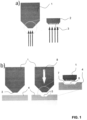
- FIG. 1 b The actual embossing on the device to be made identifiable is illustrated in Figure 1 b) .
- the metal stamp 1 is pressed onto the surface of the corresponding device 4 until an embossed region 5 is formed under plastic deformation conditions.
- the result is a general indentation 7 in the region where the grating of the patch is generated.
- a grating 6, which essentially corresponds to the complementary topologically structured surface to the one in the metal stamp is generated on the surface of the device 4.
- the proposed method consists in hammering the desired microstructure into the surface of the device to be securitized by an embossing method using a main die in the form of the metal stamp.
- This metal stamp can be nano- and/or microstructured with the ionic etching method described above, it may however also itself have been produced in an embossing process.
- a main die of hardened steel for example, is advantageous and an embossing pressure of approximately 0.1-5 kN/mm 2 is required, preferably in the range 0.1-2 kN/mm 2 .
- the main die may also be made of hardened steel with a coating of tungsten carbide, Si 3 N 4 or ZrO 2 , for example, which carries the microstructure. The latter embodiment is less expensive because only the coating must be made of the very hard and fracture-resistant material.
- Figure 1 c) and d ) show that the corresponding process can be used for different medical devices, and the corresponding optical patches can be applied at different places in these devices.
- the device 4' is a medical distance holder ring.
- the device is an implant 9.
- the dental implant 9 comprises an apical threading region 11 and a coronal collar region 10.
- the apical threading region is provided with a rough surface (by chemical treatment and/or mechanical treatment) which is not suitable for the generation of a grating 6.
- the collar region 10, and in particular axial circumferential surfaces such as the lower abutment surface 12 or the upper terminal surface 13 are suitable for embossing the corresponding optically variable grating patch.
- the embossing is not limited to flat surfaces such as illustrated in figure 1 , the embossing process has the advantage of also being suitable for convex and/or concave surfaces.
- any kind of surface can be embossed, all that needs to be taken care of is that the general surface form on the tip 3' of the metal stamp 1 should be complementary to the general surface form of the section of the device 4" where the grating patches to be applied.
- FIG. 3 Other possibilities of locating a corresponding embossed grating 6 on implants are illustrated in figure 3 .
- an embossed grating 6 can be generated on the radial surface 15 of the dental implant which is either converging apically as illustrated in this figure, or also the opposite, if the corresponding surface is converging coronally.
- the corresponding embossed grating 6 can be generated on an abutment 17, specifically on a frustoconical section 18 thereof. While not being illustrated in figure 3 on the right-hand side, it is also possible to generate corresponding patches in a lower apical region of the abutment 17, for example in one of the contact surfaces contacting the implant in use.
- Figure 4 illustrates the surface topology on the metal stamp, using the methods as described above a nice grating can be generated if for example a grating period of 1.8 ⁇ m is used.
- the grating has a depth of approximately 360 nm.
- the grating can be generated over the full patch and it comprises only little lattice imperfections.
- Figure 5 demonstrates that even after having been used repeatedly, the corresponding metal stamp maintains the essential properties of the topologically structured surface. After a series of embossing's in titanium material still the grating has a depth of approximately 360 nm, there is little deposition of titanium on the surface of the metal stamp.
- Figure 6 shows a dental abutment 17 in the coronally converging portion thereof there is provided a flattened region 20, and where in this flattened region the optical diffractive element with a grating 6' has been generated.
- the corresponding grating has a depth in the range of 250 nm, the proper periodicity, and the structure was generated in an abutment having a roughness value Ra of approximately 0.22 ⁇ m.
- Oppressing force of 4.5 kN was applied at room temperature resulting in a grating as illustrated in c) and d).
- 1 metal stamp 12 lower abutment surface on 10 2 front portion of 1 13 upper terminal surface on 10 3 topologically structured front surface of 1 14 interface (female) for attaching an implant 3' topologically structured 15 conical portion of 10 concave front surface of 1 16 interface (male) for attaching the abutment to the implant 3" topologically structured inclined front surface of 1 17 abutment 4 object to be provided with a grating 18 conical surface of the abutment 4' object in the form of a ring 19 measurement line 4" object with convex surface 20 flattened portion on 18 with optical diffractive element 5 embossed region in 4 6 grating embossed in 4 6' grating in the form of a diffractive optical element 30 master tool 30a master 3D topologically structured surface 7 general indentation 8 embossing force 31 soft stamp 9 dental implant 31a soft stamp 3D topologically structured surface 10 coronal collar region of 9 11 apical threading region of 9 32 imprint 32a imprint 3D topologically
Claims (15)
- Procédé de fabrication d'un tampon métallique (1) pour l'estampage d'une nanostructure et/ou d'une microstructure sur un dispositif métallique (4), dans lequel le procédé comprend au moins les étapes suivantes dans un ordre donné pour produire une zone d'estampage à structure topologique 3D (3) sur au moins une partie de la surface du tampon métallique (1) :a) fournir un outil maître (30) ayant une surface topologique 3D maîtresse (30a) représentant ladite nanostructure et/ou microstructure, et reproduire ladite surface topologique 3D maîtresse (30a) dans la surface d'un tampon souple (31) pour former une surface topologique 3D de tampon souple (31a) ;b) former une empreinte (32) sur la surface topologiquement structurée en 3D du tampon souple (31a) à l'aide d'un matériau organique polymérisable et/ou réticulable pour former une surface topologiquement structurée en 3D (32a) sur une face de l'empreinte (32), avant, pendant ou après la mise en contact d'une face opposée de l'empreinte (32) avec ladite partie de la surface du tampon métallique (1), et retirer ledit tampon souple (31) en exposant ladite surface topologiquement structurée en 3D (32a) de l'empreinte ;c) ouverture par gravure de ladite surface topologiquement structurée en 3D (32a) pour exposer à l'air uniquement les parties les plus en retrait de la surface topologiquement structurée en 3D (32a) à l'aide d'un premier ensemble de conditions de gravure ;d) en utilisant un deuxième ensemble de conditions de gravure, différent du premier ensemble de conditions de gravure, graver la surface métallique du poinçon métallique (1) pour former ladite zone de gaufrage à structure topologique 3D (3), la gravure du métal dans cette étape étant effectuée à l'aide d'une gravure par faisceau d'ions réactifs (RIBE) ou d'un fraisage par faisceau d'ions (IBM).
- Méthode selon la revendication 1, dans laquelle la nano- et/ou microstructure est un élément diffractif optique avec un réseau (6).
- Procédé selon l'une quelconque des revendications précédentes, dans lequel, avant l'étape a) et/ou b), la surface du tampon métallique pour la zone de gaufrage (3) est polie, de préférence à l'aide de techniques de polissage mécanique, chimique ou combinant mécanique et chimique, de préférence jusqu'à ce qu'une rugosité de surface Ra, telle que définie selon la norme ISO 4287:1997, d'au plus 0,8 µm, de préférence d'au plus 0,5 µm ou d'au plus 0,3 µm ou d'au plus 0,23 µm soit établie au moins dans la surface du tampon métallique pour la zone de gaufrage (3).
- Méthode selon l'une quelconque des revendications précédentes, dans laquelle l'outil maître (30) est fabriqué à partir d'un matériau photorésistant, de verre, d'une cale en nickel, d'un maître en silice fondue, d'une réplique sol-gel ou d'une combinaison de ceux-ci.
- Procédé selon l'une quelconque des revendications précédentes, dans lequel le matériau du tampon souple, qui est de préférence élastomère, est un matériau polymère ou oligomère choisi dans le groupe constitué par : les matériaux à base de silicium, de préférence les élastomères à base d'organosilicium tels que le PDMS, les matériaux à base d'uréthane, les matériaux à base de polyéthylène tels que le polyéthylène téréphtalate, les matériaux à base de polypropylène, les polyacrylates tels que le polyméthacrylate de méthyle (PMMA), l'ester éthylique d'acide polyméthacrylique (PMAA), l'ester propylique de l'acide polyméthacrylique (PMAP), l'ester isopropylique de l'acide polyméthacrylique, le polycarbonate (PC), le polyester (PES), les polyamides aliphatiques ou (semi-)aromatiques (PA), les polymères halogénés tels que les polymères fluorés, notamment l'ETFE ou le PTFE, le polyimide (PI), ainsi que leurs mélanges et/ou leurs copolymères,et/ou dans lequel, à l'étape a), la réplication de la surface topologique 3D maîtresse (30a) est réalisée par gaufrage à chaud ou à froid, gaufrage UV, coulage UV, coulage à chaud ou coulage à chaud et à UV, ou une combinaison de ces procédés, et/ou dans lequel le tampon souple (31) est coulé ou laminé sur un support de préférence souple, de préférence une feuille d'aluminium,et/ou dans lequel, avant l'étape b), le matériau souple du tampon est durci et/ou réticulé et/ou polymérisé.
- Procédé selon l'une quelconque des revendications précédentes, dans lequel le matériau d'impression organique polymérisable et/ou réticulable est choisi dans le groupe constitué par : un matériau à base d'acrylate, y compris les matériaux à base de méthacrylate, un matériau à base de polyester, un matériau à base d'époxy ou un matériau à base d'uréthane, ou des mélanges et/ou des copolymères et/ou des formes de greffons de ceux-ci ;et/ou dans lequel le matériau d'impression organique polymérisable et/ou réticulable est un matériau à deux composants, de préférence à base d'un matériau choisi dans le groupe consistant en : un matériau à base d'acrylate, y compris les matériaux à base de méthacrylate, un matériau à base de polyester, un matériau à base d'époxy ou un matériau à base d'uréthane, ou des mélanges et/ou des copolymères et/ou des formes de greffons de ceux-ci ;et/ou dans lequel, à l'étape b), avant ou après avoir retiré ledit tampon souple (31), le matériau de l'empreinte (32) est réticulé et/ou polymérisé par irradiation et/ou chaleur, de préférence par irradiation UV,et/ou dans lequel, à l'étape b), le matériau d'impression organique polymérisable et/ou réticulable est déposé sur le tampon souple (31) à l'aide d'une technique d'enduction, de préférence l'enduction par fente, l'enduction par coulée, l'enduction par centrifugation, l'enduction par pulvérisation ou une combinaison de ces techniques,et/ou dans lequel l'application de l'empreinte (32) sur le tampon métallique (1) implique de presser le matériau d'empreinte situé entre le tampon souple (31) et le tampon métallique (1), de préférence à l'aide d'un tampon, de préférence un tampon élastomère déformable,et/ou dans lequel un matériau antiadhésif est appliqué sur la surface topologique 3D du tampon souple (31a) avant la mise en contact avec le matériau d'impression organique polymérisable et/ou réticulable.
- Méthode selon l'une quelconque des revendications précédentes, dans laquelle l'ouverture de la gravure à l'étape c) est effectuée à l'aide d'une technique de gravure sèche, y compris la gravure par réaction ionique (RIE), dans laquelle on utilise de préférence un plasma à base d'oxygène sous vide.
et/ou dans lequel la gravure du métal à l'étape d) est effectuée à l'aide d'une gravure par faisceau d'ions réactifs (RIBE) ou d'un fraisage par faisceau d'ions (IBM) dans lequel un gaz argon est ionisé et projeté sur la surface du poinçon métallique ; et/ou dans lequel, après l'étape d), l'empreinte résiduelle, si elle est présente, est nettoyée de la surface. - Procédé selon l'une quelconque des revendications précédentes, dans lequel, au moins dans la région de la zone de gaufrage à structure topologique 3D (3), le tampon métallique est en acier, de préférence en acier trempé.
- Procédé de génération d'une nano- et/ou microstructure, de préférence sous la forme d'un élément optique diffractif en forme de réseau, sur un dispositif métallique, dans lequel un tampon métallique (1) fabriqué à l'aide d'un procédé selon l'une des revendications 1-8 portant une surface topologiquement structurée (3) étant essentiellement le négatif de la nano- et/ou microstructure (6) à générer sur le dispositif (4) est estampé sur une surface métallique exposée du dispositif dans des conditions de déformation plastique de telle sorte que la topologie de la surface topologiquement structurée est imagée sur la surface métallique du dispositif (4), où, de préférence, le tampon métallique a une profondeur de réseau comprise entre 80 et 500 nm, de préférence entre 200 et 400 nm, et plus préférentiellement entre 230 et 300 nm.
- Procédé selon la revendication 9, dans lequel le poinçon métallique (1), au moins dans la zone de la surface topologiquement structurée (3) pour le gaufrage, est constitué d'un matériau d'une dureté supérieure à celle du matériau du dispositif (4) dans la zone exposée à gaufrer, le poinçon métallique étant de préférence essentiellement à base d'acier trempé, ou d'acier trempé avec un revêtement de carbure de tungstène, de Si3N4 ou de ZrO2.
- Méthode selon l'une des revendications précédentes 9-10, dans laquelle la nano-et/ou microstructure, de préférence le réseau (6), est gaufrée à l'aide d'une pression de gaufrage comprise entre 0,1 et 5 kN/mm2 , de préférence entre 0,1 et 2 kN/mm.2 et/ou dans lequel le réseau est gaufré à une température maximale de 150°C, de préférence maximale de 100°C, de préférence comprise entre 10 et 40°C.
- Dispositif (4) consistant essentiellement en une pièce structurelle portante en métal, à l'exception d'une prothèse médicale (9, 17), d'un dispositif médical d'ostéosynthèse, d'une prothèse auditive ou d'un boîtier de prothèse auditive,
dans lequel le dispositif (4, 9, 17) comprend au moins une nano et/ou microstructure sous la forme d'un élément optique diffractif avec un réseau (6), qui est directement embossé dans une surface métallique exposée de la partie porteuse sous la forme d'un élément de sécurité et/ou d'identification, en utilisant un tampon métallique fabriqué selon l'une des revendications précédentes 1-8 et/ou en utilisant une méthode selon l'une des revendications précédentes 9-11. - Dispositif selon la revendication 12, dans lequel le métal de la partie structurelle portante du dispositif est choisi parmi l'acier, de préférence l'acier inoxydable, ou le titane ou un alliage de titane avec au moins un des éléments suivants : zinc, niobium, tantale, vanadium, aluminium, etc.
et dans lequel, de préférence, les élévations les plus saillantes de la nanostructure et/ou de la microstructure, de préférence la grille, sont au niveau de la surface environnante de la partie structurelle porteuse et par rapport à la surface environnante, ou sont en retrait par rapport à la surface environnante de moins de 40 microns, de préférence de moins de 20 microns. - Dispositif selon l'une des revendications précédentes 12 - 13, dans lequel la période de la nano- et/ou microstructure de l'élément optique diffractif avec un réseau (6) dans la surface métallique exposée de la partie structurelle portante du dispositif, de préférence le réseau, est de l'ordre de 0,3-3 µm ou de l'ordre de 0,5-2 µm, de préférence de l'ordre de 1-1,9 µm ou de 1,7-1,9 µm.et/ou dans lequel la profondeur de la nanostructure et/ou de la microstructure de l'élément optique diffractif à réseau (6) dans la surface métallique exposée de la partie structurelle portante du dispositif, de préférence le réseau, est comprise entre 80 et 500 nm, de préférence entre 200 et 400 nm, et plus préférentiellement entre 230 et 300 nm.et/ou dans lequel la nanostructure et/ou la microstructure de l'élément optique diffractif avec un réseau (6) dans la surface métallique exposée de la partie structurelle portante du dispositif, de préférence le réseau (6), est embossée sur une partie métallique exposée au sol du dispositif,et/ou dans lequel la nano et/ou microstructure de l'élément optique diffractif avec un réseau (6) dans la surface métallique exposée de la partie structurelle portante du dispositif, de préférence le réseau (6), est embossée sur une partie métallique exposée du dispositif ayant une rugosité de surface Ra, telle que définie selon ISO 4287: 1997, d'au plus 0,8 µm, de préférence d'au plus 0,5 µm ou d'au plus 0,3 µm ou d'au plus 0,23 µm, de préférence dans la plage de 0,20 à 0,25 µm,et/ou dans lequel la nano et/ou microstructure de l'élément optique diffractif avec un réseau (6) dans la surface métallique exposée de la partie structurelle portante du dispositif, de préférence le réseau (6), est gaufrée en utilisant une pression de gaufrage dans la plage de 0,1-5 kN/mm2 , de préférence dans la plage de 0,1-2kN/mm2et/ou dans lequel le réseau de l'élément optique diffractif avec un réseau (6) dans la surface métallique exposée de la partie structurelle portante du dispositif est embossé à une température d'au plus 150°C, de préférence d'au plus 100°C, de préférence dans la plage de 10-40°C,et/ou dans lequel la nanostructure et/ou la microstructure de l'élément optique diffractif avec un réseau (6) dans la surface métallique exposée de la partie structurelle portante du dispositif, de préférence le réseau, est telle que les pointes du réseau sont essentiellement alignées avec le plan de surface défini par la surface métallique environnanteet/ou dans lequel l'élément optique diffractif de l'élément optique diffractif avec un réseau (6) dans la surface métallique exposée de la partie structurelle portante du dispositif génère l'image d'une image et/ou de lettres et/ou de chiffres et/ou de pictogrammes.
- Dispositif selon l'une des revendications précédentes 12-14, dans lequel le dispositif estou d'une montre, la nano- et/ou microstructure, de préférence le réseau, étant prévue notamment pour la traçabilité ou l'anti-contrefaçon notamment des pièces en titane ou en alliage de titane,partie ou outil chirurgical, la nano- et/ou microstructure, de préférence le réseau,étant prévue notamment pour le suivi et la traçabilité ou la lutte contre la contrefaçon,partie d'un système médical ou aide médicale pouvant être implantée dans le corps humain, à l'exception d'une prothèse médicale, d'un dispositif médical d'ostéosynthèse ou d'un appareil auditif ou d'un boîtier d'appareil auditif, la nanostructure et/ou la microstructure, de préférence le réseau, étant prévue pour le suivi et la traçabilité ou la lutte contre la contrefaçon, en particulier des pièces en titane ou en alliage de titane,une partie ou la totalité d'un dispositif automobile, aéronautique, militaire, d'une centrale électrique, d'un ordinateur grand public, la nano et/ou microstructure, de préférence le réseau, étant prévue notamment pour le suivi et la traçabilité ou la lutte contre la contrefaçon des pièces en titane ou en alliage de titane en particulier, ou à des fins décoratives.
Priority Applications (3)
| Application Number | Priority Date | Filing Date | Title |
|---|---|---|---|
| EP18164630.8A EP3547026B1 (fr) | 2018-03-28 | 2018-03-28 | Procédé de fabrication d'un tampon métallique pour le gaufrage d'une nano et/ou microstructure sur un dispositif métallique ainsi que ses utilisations et dispositifs fabriqués à partir de celui-ci |
| US16/366,433 US20190299266A1 (en) | 2018-03-28 | 2019-03-27 | Method for producing a metal stamp for embossing a nano-and/or microstructure on a metal device as well as uses thereof and devices made therewith |
| CN201910244823.1A CN110320743A (zh) | 2018-03-28 | 2019-03-28 | 制作冲压纳米和/或微米结构的金属印模的方法及装置 |
Applications Claiming Priority (1)
| Application Number | Priority Date | Filing Date | Title |
|---|---|---|---|
| EP18164630.8A EP3547026B1 (fr) | 2018-03-28 | 2018-03-28 | Procédé de fabrication d'un tampon métallique pour le gaufrage d'une nano et/ou microstructure sur un dispositif métallique ainsi que ses utilisations et dispositifs fabriqués à partir de celui-ci |
Publications (2)
| Publication Number | Publication Date |
|---|---|
| EP3547026A1 EP3547026A1 (fr) | 2019-10-02 |
| EP3547026B1 true EP3547026B1 (fr) | 2023-11-29 |
Family
ID=61832421
Family Applications (1)
| Application Number | Title | Priority Date | Filing Date |
|---|---|---|---|
| EP18164630.8A Active EP3547026B1 (fr) | 2018-03-28 | 2018-03-28 | Procédé de fabrication d'un tampon métallique pour le gaufrage d'une nano et/ou microstructure sur un dispositif métallique ainsi que ses utilisations et dispositifs fabriqués à partir de celui-ci |
Country Status (3)
| Country | Link |
|---|---|
| US (1) | US20190299266A1 (fr) |
| EP (1) | EP3547026B1 (fr) |
| CN (1) | CN110320743A (fr) |
Families Citing this family (1)
| Publication number | Priority date | Publication date | Assignee | Title |
|---|---|---|---|---|
| CN113547012B (zh) * | 2021-07-21 | 2022-04-12 | 哈尔滨工业大学(威海) | 复合金属薄板微型阵列功能结构件及其成形方法及其装置 |
Citations (3)
| Publication number | Priority date | Publication date | Assignee | Title |
|---|---|---|---|---|
| US5728324A (en) * | 1995-01-31 | 1998-03-17 | Digital Optics Corporation | Molding diffractive optical elements |
| US20090325107A1 (en) * | 2008-06-25 | 2009-12-31 | Micron Technology, Inc. | Thermal embossing of resist reflowed lenses to make aspheric lens master wafer |
| US20100301004A1 (en) * | 2009-05-29 | 2010-12-02 | Babak Heidari | Fabrication of metallic stamps for replication technology |
Family Cites Families (13)
| Publication number | Priority date | Publication date | Assignee | Title |
|---|---|---|---|---|
| US4734157A (en) * | 1985-08-27 | 1988-03-29 | International Business Machines Corporation | Selective and anisotropic dry etching |
| US6849558B2 (en) * | 2002-05-22 | 2005-02-01 | The Board Of Trustees Of The Leland Stanford Junior University | Replication and transfer of microstructures and nanostructures |
| US7488343B2 (en) * | 2003-09-16 | 2009-02-10 | Boston Scientific Scimed, Inc. | Medical devices |
| US8076386B2 (en) * | 2004-02-23 | 2011-12-13 | Molecular Imprints, Inc. | Materials for imprint lithography |
| FR2901909B1 (fr) * | 2006-05-30 | 2008-10-24 | Commissariat Energie Atomique | Memoire de donnees inscriptible et lisible par micropointes, structuree en caissons, et procede de fabrication |
| DE102007044504A1 (de) * | 2007-09-18 | 2009-03-19 | Robert Bosch Gmbh | Verfahren zum Aufdrucken einer Nano- und/oder Mikrostruktur, Stempel sowie Substrat |
| US9122148B2 (en) * | 2008-11-03 | 2015-09-01 | Canon Nanotechnologies, Inc. | Master template replication |
| CN101477304B (zh) * | 2008-11-04 | 2011-08-17 | 南京大学 | 在复杂形状表面复制高分辨率纳米结构的压印方法 |
| EP2531888A1 (fr) * | 2010-02-05 | 2012-12-12 | Obducat AB | Procédé et processus permettant une reproduction de poinçon métallique pour des nanomotifs de grande surface |
| GB201100405D0 (en) * | 2011-01-11 | 2011-02-23 | Depuy Ireland | Surgical instrument and method of marking a surgical instrument |
| SG11201500437VA (en) * | 2012-07-25 | 2015-02-27 | Suisse Electronique Microtech | Method to optimize a light coupling waveguide |
| CA2912888C (fr) * | 2014-11-25 | 2018-04-03 | Hao Jiang | Procedes de fabrication de dispositifs d'affichage d'image en couleur comportant des pixels de couleur structuraux a partir d'un modele generique |
| AT516558B1 (de) * | 2014-12-10 | 2018-02-15 | Joanneum Res Forschungsgmbh | Prägelack, Verfahren zum Prägen sowie mit dem Prägelack beschichtete Substratoberfläche |
-
2018
- 2018-03-28 EP EP18164630.8A patent/EP3547026B1/fr active Active
-
2019
- 2019-03-27 US US16/366,433 patent/US20190299266A1/en not_active Abandoned
- 2019-03-28 CN CN201910244823.1A patent/CN110320743A/zh active Pending
Patent Citations (3)
| Publication number | Priority date | Publication date | Assignee | Title |
|---|---|---|---|---|
| US5728324A (en) * | 1995-01-31 | 1998-03-17 | Digital Optics Corporation | Molding diffractive optical elements |
| US20090325107A1 (en) * | 2008-06-25 | 2009-12-31 | Micron Technology, Inc. | Thermal embossing of resist reflowed lenses to make aspheric lens master wafer |
| US20100301004A1 (en) * | 2009-05-29 | 2010-12-02 | Babak Heidari | Fabrication of metallic stamps for replication technology |
Also Published As
| Publication number | Publication date |
|---|---|
| US20190299266A1 (en) | 2019-10-03 |
| EP3547026A1 (fr) | 2019-10-02 |
| CN110320743A (zh) | 2019-10-11 |
Similar Documents
| Publication | Publication Date | Title |
|---|---|---|
| JP5276436B2 (ja) | 中間スタンプによるパターン複製 | |
| EP1731961B1 (fr) | Méthode pour la reproduction d'un modèle | |
| Stormonth-Darling et al. | Injection moulding of ultra high aspect ratio nanostructures using coated polymer tooling | |
| JP5525707B2 (ja) | 電子デバイスのための一組の構造を形成する方法 | |
| US20100046825A1 (en) | Authentication and anticounterfeiting methods and devices | |
| JP5424645B2 (ja) | 光学製品上にミクロン―スケールのパターンを転写する方法、及びこれを用いた光学製品 | |
| EP3547026B1 (fr) | Procédé de fabrication d'un tampon métallique pour le gaufrage d'une nano et/ou microstructure sur un dispositif métallique ainsi que ses utilisations et dispositifs fabriqués à partir de celui-ci | |
| JP2008304701A (ja) | 凹凸パターン形成シートおよびその製造方法、光拡散体製造用工程シート原版ならびに光拡散体の製造方法 | |
| EP3545908B1 (fr) | Prothèses médicales, dispositifs médicaux ostéosynthétiques ou prothèses auditives comportant des éléments de sécurité et/ou d'identification | |
| US10146128B2 (en) | Tool surface nano-structure patterning process | |
| Scheer et al. | Nanoimprint techniques | |
| JP5482401B2 (ja) | ナノバックリング形状を有する表面微細凹凸体の製造方法、光学素子の製造方法、及び2次工程シートの製造方法。 | |
| TW200901188A (en) | Method of making an optical disc | |
| EP1731965B1 (fr) | Timbre d'impression comprenant un copolymère oléfine cyclique | |
| Mukherjee et al. | Adhesive force assisted imprinting of soft solid polymer films by flexible foils | |
| US20090080323A1 (en) | Device and Method for Obtaining a Substrate Structured on Micrometric or Nanometric Scale | |
| JP2012250357A (ja) | 偽造防止用粒子及びその製造方法、偽造防止用インク、偽造防止用シート、有価証券、カード | |
| WO2020209331A1 (fr) | Structure optique, feuille de transfert, article et procédé de fabrication de structure optique | |
| US8647552B2 (en) | Method for enhancing hardness of nanoimprint mold | |
| EP4202547B1 (fr) | Procédé de fabrication de guide d'onde optique | |
| KR20190020914A (ko) | 가압방식 소성변형 패터닝 방법 | |
| JP7147447B2 (ja) | 樹脂製モールド、及び光学素子の製造方法 | |
| US20230176475A1 (en) | Conformal micro- or nanopatterned nanoimprint lithography master and methods of making and using the same | |
| Lee et al. | Replication of nanostructures on microstructures by intermediate film mold inserted hot embossing process | |
| Jacot-Descombes et al. | Advancing manufacturing route for multi-level diffractive optical elements by combining nanoimprint lithography and LiGA process |
Legal Events
| Date | Code | Title | Description |
|---|---|---|---|
| PUAI | Public reference made under article 153(3) epc to a published international application that has entered the european phase |
Free format text: ORIGINAL CODE: 0009012 |
|
| STAA | Information on the status of an ep patent application or granted ep patent |
Free format text: STATUS: THE APPLICATION HAS BEEN PUBLISHED |
|
| AK | Designated contracting states |
Kind code of ref document: A1 Designated state(s): AL AT BE BG CH CY CZ DE DK EE ES FI FR GB GR HR HU IE IS IT LI LT LU LV MC MK MT NL NO PL PT RO RS SE SI SK SM TR |
|
| AX | Request for extension of the european patent |
Extension state: BA ME |
|
| STAA | Information on the status of an ep patent application or granted ep patent |
Free format text: STATUS: REQUEST FOR EXAMINATION WAS MADE |
|
| 17P | Request for examination filed |
Effective date: 20200319 |
|
| RBV | Designated contracting states (corrected) |
Designated state(s): AL AT BE BG CH CY CZ DE DK EE ES FI FR GB GR HR HU IE IS IT LI LT LU LV MC MK MT NL NO PL PT RO RS SE SI SK SM TR |
|
| STAA | Information on the status of an ep patent application or granted ep patent |
Free format text: STATUS: EXAMINATION IS IN PROGRESS |
|
| 17Q | First examination report despatched |
Effective date: 20220414 |
|
| GRAP | Despatch of communication of intention to grant a patent |
Free format text: ORIGINAL CODE: EPIDOSNIGR1 |
|
| STAA | Information on the status of an ep patent application or granted ep patent |
Free format text: STATUS: GRANT OF PATENT IS INTENDED |
|
| RAP3 | Party data changed (applicant data changed or rights of an application transferred) |
Owner name: CSEM CENTRE SUISSE D'ELECTRONIQUE ET DE MICROTECHNIQUE SA |
|
| INTG | Intention to grant announced |
Effective date: 20230714 |
|
| RIN1 | Information on inventor provided before grant (corrected) |
Inventor name: MAREK, ROMY LINDA Inventor name: DE WILD, MICHAEL Inventor name: KRAEHENBUEHL, ROGER Inventor name: KALLWEIT, DAVID Inventor name: SCHNIEPER, MARC Inventor name: LUU-DINH, ANGELIQUE Inventor name: SCHNEIDER, CHRISTIAN |
|
| GRAS | Grant fee paid |
Free format text: ORIGINAL CODE: EPIDOSNIGR3 |
|
| GRAA | (expected) grant |
Free format text: ORIGINAL CODE: 0009210 |
|
| STAA | Information on the status of an ep patent application or granted ep patent |
Free format text: STATUS: THE PATENT HAS BEEN GRANTED |
|
| AK | Designated contracting states |
Kind code of ref document: B1 Designated state(s): AL AT BE BG CH CY CZ DE DK EE ES FI FR GB GR HR HU IE IS IT LI LT LU LV MC MK MT NL NO PL PT RO RS SE SI SK SM TR |
|
| REG | Reference to a national code |
Ref country code: GB Ref legal event code: FG4D |
|
| REG | Reference to a national code |
Ref country code: CH Ref legal event code: EP |
|
| REG | Reference to a national code |
Ref country code: DE Ref legal event code: R096 Ref document number: 602018061715 Country of ref document: DE |
|
| REG | Reference to a national code |
Ref country code: IE Ref legal event code: FG4D |
|
| REG | Reference to a national code |
Ref country code: LT Ref legal event code: MG9D |
|
| REG | Reference to a national code |
Ref country code: NL Ref legal event code: MP Effective date: 20231129 |
|
| PG25 | Lapsed in a contracting state [announced via postgrant information from national office to epo] |
Ref country code: GR Free format text: LAPSE BECAUSE OF FAILURE TO SUBMIT A TRANSLATION OF THE DESCRIPTION OR TO PAY THE FEE WITHIN THE PRESCRIBED TIME-LIMIT Effective date: 20240301 |
|
| PG25 | Lapsed in a contracting state [announced via postgrant information from national office to epo] |
Ref country code: IS Free format text: LAPSE BECAUSE OF FAILURE TO SUBMIT A TRANSLATION OF THE DESCRIPTION OR TO PAY THE FEE WITHIN THE PRESCRIBED TIME-LIMIT Effective date: 20240329 |
|
| PG25 | Lapsed in a contracting state [announced via postgrant information from national office to epo] |
Ref country code: LT Free format text: LAPSE BECAUSE OF FAILURE TO SUBMIT A TRANSLATION OF THE DESCRIPTION OR TO PAY THE FEE WITHIN THE PRESCRIBED TIME-LIMIT Effective date: 20231129 |
|
| PG25 | Lapsed in a contracting state [announced via postgrant information from national office to epo] |
Ref country code: ES Free format text: LAPSE BECAUSE OF FAILURE TO SUBMIT A TRANSLATION OF THE DESCRIPTION OR TO PAY THE FEE WITHIN THE PRESCRIBED TIME-LIMIT Effective date: 20231129 |
|
| PG25 | Lapsed in a contracting state [announced via postgrant information from national office to epo] |
Ref country code: LT Free format text: LAPSE BECAUSE OF FAILURE TO SUBMIT A TRANSLATION OF THE DESCRIPTION OR TO PAY THE FEE WITHIN THE PRESCRIBED TIME-LIMIT Effective date: 20231129 Ref country code: IS Free format text: LAPSE BECAUSE OF FAILURE TO SUBMIT A TRANSLATION OF THE DESCRIPTION OR TO PAY THE FEE WITHIN THE PRESCRIBED TIME-LIMIT Effective date: 20240329 Ref country code: GR Free format text: LAPSE BECAUSE OF FAILURE TO SUBMIT A TRANSLATION OF THE DESCRIPTION OR TO PAY THE FEE WITHIN THE PRESCRIBED TIME-LIMIT Effective date: 20240301 Ref country code: ES Free format text: LAPSE BECAUSE OF FAILURE TO SUBMIT A TRANSLATION OF THE DESCRIPTION OR TO PAY THE FEE WITHIN THE PRESCRIBED TIME-LIMIT Effective date: 20231129 Ref country code: BG Free format text: LAPSE BECAUSE OF FAILURE TO SUBMIT A TRANSLATION OF THE DESCRIPTION OR TO PAY THE FEE WITHIN THE PRESCRIBED TIME-LIMIT Effective date: 20240229 |
|
| PGFP | Annual fee paid to national office [announced via postgrant information from national office to epo] |
Ref country code: DE Payment date: 20240321 Year of fee payment: 7 Ref country code: GB Payment date: 20240327 Year of fee payment: 7 |