EP3547015A1 - Manufacturing method for coa type liquid crystal panel, and coa type liquid crystal panel - Google Patents
Manufacturing method for coa type liquid crystal panel, and coa type liquid crystal panel Download PDFInfo
- Publication number
- EP3547015A1 EP3547015A1 EP16922378.1A EP16922378A EP3547015A1 EP 3547015 A1 EP3547015 A1 EP 3547015A1 EP 16922378 A EP16922378 A EP 16922378A EP 3547015 A1 EP3547015 A1 EP 3547015A1
- Authority
- EP
- European Patent Office
- Prior art keywords
- layer
- insulative
- color resist
- insulative layer
- metal layer
- Prior art date
- Legal status (The legal status is an assumption and is not a legal conclusion. Google has not performed a legal analysis and makes no representation as to the accuracy of the status listed.)
- Withdrawn
Links
- 239000004973 liquid crystal related substance Substances 0.000 title claims abstract description 45
- 238000004519 manufacturing process Methods 0.000 title claims abstract description 19
- 229910052751 metal Inorganic materials 0.000 claims abstract description 71
- 239000002184 metal Substances 0.000 claims abstract description 71
- 238000000059 patterning Methods 0.000 claims abstract description 15
- 239000000758 substrate Substances 0.000 claims description 46
- 238000000034 method Methods 0.000 claims description 38
- 239000004065 semiconductor Substances 0.000 claims description 24
- 230000008569 process Effects 0.000 claims description 15
- 238000000151 deposition Methods 0.000 claims description 9
- 239000000463 material Substances 0.000 claims description 9
- AMGQUBHHOARCQH-UHFFFAOYSA-N indium;oxotin Chemical group [In].[Sn]=O AMGQUBHHOARCQH-UHFFFAOYSA-N 0.000 claims description 7
- 239000011248 coating agent Substances 0.000 claims description 5
- 238000000576 coating method Methods 0.000 claims description 5
- 238000002161 passivation Methods 0.000 claims description 5
- 229910021417 amorphous silicon Inorganic materials 0.000 description 8
- 239000010408 film Substances 0.000 description 6
- 229910004205 SiNX Inorganic materials 0.000 description 5
- 230000015572 biosynthetic process Effects 0.000 description 4
- 238000005516 engineering process Methods 0.000 description 4
- 239000011521 glass Substances 0.000 description 4
- 239000011159 matrix material Substances 0.000 description 4
- 230000009286 beneficial effect Effects 0.000 description 1
- 230000008878 coupling Effects 0.000 description 1
- 238000010168 coupling process Methods 0.000 description 1
- 238000005859 coupling reaction Methods 0.000 description 1
- 230000005611 electricity Effects 0.000 description 1
- 238000005530 etching Methods 0.000 description 1
- 238000012986 modification Methods 0.000 description 1
- 230000004048 modification Effects 0.000 description 1
- 230000005855 radiation Effects 0.000 description 1
- 230000009467 reduction Effects 0.000 description 1
- 230000010076 replication Effects 0.000 description 1
- 239000010409 thin film Substances 0.000 description 1
Images
Classifications
-
- G—PHYSICS
- G02—OPTICS
- G02F—OPTICAL DEVICES OR ARRANGEMENTS FOR THE CONTROL OF LIGHT BY MODIFICATION OF THE OPTICAL PROPERTIES OF THE MEDIA OF THE ELEMENTS INVOLVED THEREIN; NON-LINEAR OPTICS; FREQUENCY-CHANGING OF LIGHT; OPTICAL LOGIC ELEMENTS; OPTICAL ANALOGUE/DIGITAL CONVERTERS
- G02F1/00—Devices or arrangements for the control of the intensity, colour, phase, polarisation or direction of light arriving from an independent light source, e.g. switching, gating or modulating; Non-linear optics
- G02F1/01—Devices or arrangements for the control of the intensity, colour, phase, polarisation or direction of light arriving from an independent light source, e.g. switching, gating or modulating; Non-linear optics for the control of the intensity, phase, polarisation or colour
- G02F1/13—Devices or arrangements for the control of the intensity, colour, phase, polarisation or direction of light arriving from an independent light source, e.g. switching, gating or modulating; Non-linear optics for the control of the intensity, phase, polarisation or colour based on liquid crystals, e.g. single liquid crystal display cells
- G02F1/133—Constructional arrangements; Operation of liquid crystal cells; Circuit arrangements
- G02F1/1333—Constructional arrangements; Manufacturing methods
-
- G—PHYSICS
- G02—OPTICS
- G02F—OPTICAL DEVICES OR ARRANGEMENTS FOR THE CONTROL OF LIGHT BY MODIFICATION OF THE OPTICAL PROPERTIES OF THE MEDIA OF THE ELEMENTS INVOLVED THEREIN; NON-LINEAR OPTICS; FREQUENCY-CHANGING OF LIGHT; OPTICAL LOGIC ELEMENTS; OPTICAL ANALOGUE/DIGITAL CONVERTERS
- G02F1/00—Devices or arrangements for the control of the intensity, colour, phase, polarisation or direction of light arriving from an independent light source, e.g. switching, gating or modulating; Non-linear optics
- G02F1/01—Devices or arrangements for the control of the intensity, colour, phase, polarisation or direction of light arriving from an independent light source, e.g. switching, gating or modulating; Non-linear optics for the control of the intensity, phase, polarisation or colour
- G02F1/13—Devices or arrangements for the control of the intensity, colour, phase, polarisation or direction of light arriving from an independent light source, e.g. switching, gating or modulating; Non-linear optics for the control of the intensity, phase, polarisation or colour based on liquid crystals, e.g. single liquid crystal display cells
- G02F1/133—Constructional arrangements; Operation of liquid crystal cells; Circuit arrangements
- G02F1/136—Liquid crystal cells structurally associated with a semi-conducting layer or substrate, e.g. cells forming part of an integrated circuit
- G02F1/1362—Active matrix addressed cells
- G02F1/136227—Through-hole connection of the pixel electrode to the active element through an insulation layer
-
- G—PHYSICS
- G02—OPTICS
- G02F—OPTICAL DEVICES OR ARRANGEMENTS FOR THE CONTROL OF LIGHT BY MODIFICATION OF THE OPTICAL PROPERTIES OF THE MEDIA OF THE ELEMENTS INVOLVED THEREIN; NON-LINEAR OPTICS; FREQUENCY-CHANGING OF LIGHT; OPTICAL LOGIC ELEMENTS; OPTICAL ANALOGUE/DIGITAL CONVERTERS
- G02F1/00—Devices or arrangements for the control of the intensity, colour, phase, polarisation or direction of light arriving from an independent light source, e.g. switching, gating or modulating; Non-linear optics
- G02F1/01—Devices or arrangements for the control of the intensity, colour, phase, polarisation or direction of light arriving from an independent light source, e.g. switching, gating or modulating; Non-linear optics for the control of the intensity, phase, polarisation or colour
- G02F1/13—Devices or arrangements for the control of the intensity, colour, phase, polarisation or direction of light arriving from an independent light source, e.g. switching, gating or modulating; Non-linear optics for the control of the intensity, phase, polarisation or colour based on liquid crystals, e.g. single liquid crystal display cells
- G02F1/133—Constructional arrangements; Operation of liquid crystal cells; Circuit arrangements
- G02F1/1333—Constructional arrangements; Manufacturing methods
- G02F1/1343—Electrodes
- G02F1/13439—Electrodes characterised by their electrical, optical, physical properties; materials therefor; method of making
-
- G—PHYSICS
- G02—OPTICS
- G02F—OPTICAL DEVICES OR ARRANGEMENTS FOR THE CONTROL OF LIGHT BY MODIFICATION OF THE OPTICAL PROPERTIES OF THE MEDIA OF THE ELEMENTS INVOLVED THEREIN; NON-LINEAR OPTICS; FREQUENCY-CHANGING OF LIGHT; OPTICAL LOGIC ELEMENTS; OPTICAL ANALOGUE/DIGITAL CONVERTERS
- G02F1/00—Devices or arrangements for the control of the intensity, colour, phase, polarisation or direction of light arriving from an independent light source, e.g. switching, gating or modulating; Non-linear optics
- G02F1/01—Devices or arrangements for the control of the intensity, colour, phase, polarisation or direction of light arriving from an independent light source, e.g. switching, gating or modulating; Non-linear optics for the control of the intensity, phase, polarisation or colour
- G02F1/13—Devices or arrangements for the control of the intensity, colour, phase, polarisation or direction of light arriving from an independent light source, e.g. switching, gating or modulating; Non-linear optics for the control of the intensity, phase, polarisation or colour based on liquid crystals, e.g. single liquid crystal display cells
- G02F1/133—Constructional arrangements; Operation of liquid crystal cells; Circuit arrangements
- G02F1/136—Liquid crystal cells structurally associated with a semi-conducting layer or substrate, e.g. cells forming part of an integrated circuit
- G02F1/1362—Active matrix addressed cells
- G02F1/136222—Colour filters incorporated in the active matrix substrate
-
- G—PHYSICS
- G02—OPTICS
- G02F—OPTICAL DEVICES OR ARRANGEMENTS FOR THE CONTROL OF LIGHT BY MODIFICATION OF THE OPTICAL PROPERTIES OF THE MEDIA OF THE ELEMENTS INVOLVED THEREIN; NON-LINEAR OPTICS; FREQUENCY-CHANGING OF LIGHT; OPTICAL LOGIC ELEMENTS; OPTICAL ANALOGUE/DIGITAL CONVERTERS
- G02F1/00—Devices or arrangements for the control of the intensity, colour, phase, polarisation or direction of light arriving from an independent light source, e.g. switching, gating or modulating; Non-linear optics
- G02F1/01—Devices or arrangements for the control of the intensity, colour, phase, polarisation or direction of light arriving from an independent light source, e.g. switching, gating or modulating; Non-linear optics for the control of the intensity, phase, polarisation or colour
- G02F1/13—Devices or arrangements for the control of the intensity, colour, phase, polarisation or direction of light arriving from an independent light source, e.g. switching, gating or modulating; Non-linear optics for the control of the intensity, phase, polarisation or colour based on liquid crystals, e.g. single liquid crystal display cells
- G02F1/133—Constructional arrangements; Operation of liquid crystal cells; Circuit arrangements
- G02F1/1333—Constructional arrangements; Manufacturing methods
- G02F1/1335—Structural association of cells with optical devices, e.g. polarisers or reflectors
- G02F1/133509—Filters, e.g. light shielding masks
- G02F1/133514—Colour filters
- G02F1/133519—Overcoatings
-
- G—PHYSICS
- G02—OPTICS
- G02F—OPTICAL DEVICES OR ARRANGEMENTS FOR THE CONTROL OF LIGHT BY MODIFICATION OF THE OPTICAL PROPERTIES OF THE MEDIA OF THE ELEMENTS INVOLVED THEREIN; NON-LINEAR OPTICS; FREQUENCY-CHANGING OF LIGHT; OPTICAL LOGIC ELEMENTS; OPTICAL ANALOGUE/DIGITAL CONVERTERS
- G02F1/00—Devices or arrangements for the control of the intensity, colour, phase, polarisation or direction of light arriving from an independent light source, e.g. switching, gating or modulating; Non-linear optics
- G02F1/01—Devices or arrangements for the control of the intensity, colour, phase, polarisation or direction of light arriving from an independent light source, e.g. switching, gating or modulating; Non-linear optics for the control of the intensity, phase, polarisation or colour
- G02F1/13—Devices or arrangements for the control of the intensity, colour, phase, polarisation or direction of light arriving from an independent light source, e.g. switching, gating or modulating; Non-linear optics for the control of the intensity, phase, polarisation or colour based on liquid crystals, e.g. single liquid crystal display cells
- G02F1/133—Constructional arrangements; Operation of liquid crystal cells; Circuit arrangements
- G02F1/136—Liquid crystal cells structurally associated with a semi-conducting layer or substrate, e.g. cells forming part of an integrated circuit
- G02F1/1362—Active matrix addressed cells
- G02F1/1368—Active matrix addressed cells in which the switching element is a three-electrode device
-
- G—PHYSICS
- G02—OPTICS
- G02F—OPTICAL DEVICES OR ARRANGEMENTS FOR THE CONTROL OF LIGHT BY MODIFICATION OF THE OPTICAL PROPERTIES OF THE MEDIA OF THE ELEMENTS INVOLVED THEREIN; NON-LINEAR OPTICS; FREQUENCY-CHANGING OF LIGHT; OPTICAL LOGIC ELEMENTS; OPTICAL ANALOGUE/DIGITAL CONVERTERS
- G02F2201/00—Constructional arrangements not provided for in groups G02F1/00 - G02F7/00
- G02F2201/40—Arrangements for improving the aperture ratio
Definitions
- the present disclosure relates to a field of display technology, and more specifically to a method for manufacturing a color-filter-on-array (COA) type liquid crystal panel, and a COA type liquid crystal panel that can improve a pixel aperture ratio.
- COA color-filter-on-array
- a liquid crystal display has the advantages of thinness, electricity saving, no radiation, and so on, and thereby has been widely used, for example, used in an LCD television, a mobile phone, a personal digital assistant (PDA), a digital camera, a computer screen, a laptop screen, or the like.
- LCD liquid crystal display
- the LCD includes a case, a liquid crystal panel disposed in the case, and a backlight module disposed in the case.
- the structure of liquid crystal panel mainly includes a thin film transistor (TFT) array substrate, a color filter (CF) substrate, and a liquid crystal layer between the TFT array substrate and the CF substrate.
- TFT thin film transistor
- CF color filter
- the working principle of the liquid crystal panel is that the rotation of liquid crystal molecules in the liquid crystal layer is controlled by applying a driving voltage to two glass substrates so that light produced by the backlight module can be refracted to generate an image.
- a COA technology is that a color resist layer on a CF substrate is disposed on an array substrate.
- the delay of the signals of metal traces is improved since there is a reduction of couplings between pixel electrodes and the metal traces in a COA structure.
- the COA structure can obviously reduce stray capacitances, and can improve the aperture ratio and display quality of a panel.
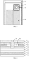
- FIG. 1 is a schematic view of the pixel design of an existing COA type liquid crystal panel.
- FIG. 2 is a profile view of a via hole and the periphery thereof in FIG. 1 .
- Each of sub-pixel areas on the array substrate of the existing COA type liquid crystal panel includes a first metal layer 21, a first insulative layer 22 disposed on the first metal layer 21, a semiconductor layer 23 disposed on the first insulative layer 22, a second metal layer 24 disposed on the semiconductor layer 23, a second insulative layer 25 disposed on the second metal layer 24, a color resist layer 26 disposed on the second insulative layer 25, a third insulative layer 27 disposed on the color resist layer 26, and a pixel electrode layer 28 disposed on the third insulative layer 27.
- a via hole 29 is formed in the second insulative layer 25, the color resist layer 26, and the third insulative layer 27, and is positioned on the second metal layer 24.
- the pixel electrode layer 28 connects to the second metal layer 24 via the via hole 29.
- a via hole structure is formed by boring a hole on an insulative layer and a color resist layer, and the diameter of the hole 261 of the color resist layer is greater than the diameter of the hole of the insulative layer.
- the via hole structure can lose a large part of a pixel aperture ratio.
- the pixel design of the existing COA type liquid crystal panel needs to be improved to simplify the manufacturing process thereof and improve the pixel aperture ratio.
- An object of the present disclosure is to provide a method for manufacturing a COA type liquid crystal panel, and a COA type liquid crystal panel that can simplify the manufacturing process thereof and improve a pixel aperture ratio.
- the present disclosure provides a method for manufacturing a COA type liquid crystal panel.
- the method includes the following steps of: providing a first substrate, and forming sequentially a first metal layer and a first insulative layer onto the first substrate; forming sequentially a color resist layer and a second insulative layer onto the first insulative layer, where the color resist layer is formed by processes such as coating, exposing, and developing, and the color resist layer is a single color resist layer, a double color resist layer, or a triple color resist layer; forming sequentially a semiconductor layer and a second metal layer onto the second insulative layer, and forming a third insulative layer covering the second insulative layer onto the second metal layer; and forming a via hole in the third insulative layer, and forming a pixel electrode layer onto the third insulative layer, where the pixel electrode layer connects to the second metal layer via the via hole.
- the present disclosure provides a method for manufacturing a COA type liquid crystal panel.
- the method includes the following steps of: providing a first substrate, and forming sequentially a first metal layer and a first insulative layer onto the first substrate; forming sequentially a color resist layer and a second insulative layer onto the first insulative layer; forming sequentially a semiconductor layer and a second metal layer onto the second insulative layer, and forming a third insulative layer covering the second insulative layer onto the second metal layer; and forming a via hole in the third insulative layer, and forming a pixel electrode layer onto the third insulative layer, where the pixel electrode layer connects to the second metal layer via the via hole.
- the present disclosure further provides a COA type liquid crystal panel including an array substrate.
- the array substrate includes a plurality of pixel areas, each of the pixel areas includes a first metal layer, a first insulative layer, a color resist layer, a second insulative layer, a semiconductor layer and a second metal layer which are sequentially formed on the second insulative layer, a third insulative layer which is disposed on the second metal layer and is coated on the second insulative layer, and a pixel electrode layer disposed on the third insulative layer in sequence; a via hole is provided on the third insulative layer, and the pixel electrode layer connects to the second metal layer via the via hole.
- the present disclosure has the following advantages. By arranging the film formation and patterning of the color resist layer before the second metal layer, a hole is bored in the third insulative layer so as to form a via hole structure. Therefore, boring on the color resist layer is avoided, the manufacturing process thereof is simplified, and the pixel aperture ratio is improved.
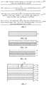
- FIG. 3 is a flow chart of a method according to an embodiment of the present disclosure for manufacturing a COA type liquid crystal panel.
- the method includes the following steps of: S31: providing a first substrate, and forming sequentially a first metal layer and a first insulative layer onto the first substrate; S32: forming sequentially a color resist layer and a second insulative layer onto the first insulative layer; S33: forming sequentially a semiconductor layer and a second metal layer onto the second insulative layer, and forming a third insulative layer covering the second insulative layer onto the second metal layer; and S34: forming a via hole in the third insulative layer, and forming a pixel electrode layer onto the third insulative layer, where the pixel electrode layer connects to the second metal layer via the via hole.
- S31 providing a first substrate, and forming sequentially a first metal layer and a first insulative layer onto the first substrate
- S32 forming sequentially a color resist layer and a second insulative
- step S31 the first substrate is provided, and the first metal layer and the first insulative layer are sequentially formed on the first substrate.
- the first metal layer is formed on the first substrate by processes such as depositing and patterning, and then the first insulative layer is deposited on the first metal layer.
- the first insulative layer can be a SiNx layer.
- the first substrate can be the array substrate of the COA type liquid crystal panel.
- the first metal layer includes a gate electrode.
- the first insulative layer is a gate electrode insulating layer disposed on the gate electrode.
- the array substrate further has a scanning line connecting the gate electrode thereon.
- step S32 the color resist layer and the second insulative layer are sequentially formed on the first insulative layer.
- the color resist layer is formed on the first insulative layer by processes such as coating, exposing, and developing, and then the second insulative layer is deposited on the color resist layer.
- the second insulative layer can be a SiNx layer.
- the color resist layer is a single color resist layer, a double color resist layer, or a triple color resist layer.
- FIGS. 4A-4C are schematic views of structures of the color resist layers of COA type liquid crystal panels according to the embodiments of the present disclosure.
- FIG. 4A shows the single color resist layer.
- the single color resist layer can be red, green, or blue, and FIG. 4A is blue (B).
- FIG. 4B shows the double color resist layer.
- the double color resist layer can be any two of red, green, and blue (no particular order), and FIG. 4B includes green (G) and red (R) in sequence.
- FIG. 4C shows the triple color resist layer.
- the triple color resist layer is a combination of red, green, or blue (no particular order), and FIG.
- 4C includes blue (B), green (G), and red (R) in sequence.
- processes such as coating, exposing, and developing are executed with three replications when the triple color resist layer is employed, thereby forming the triple color resist layer having red, green, and blue.
- step S33 the semiconductor layer and the second metal layer are sequentially formed on the second insulative layer, and the third insulative layer covering the second insulative layer is formed on the second metal layer.
- a semiconductor film is deposited on the second insulative layer.
- the semiconductor film is etched to form the semiconductor layer.
- the second metal layer is formed on the second insulative layer by processes such as depositing and patterning.
- the third insulative layer is deposited on the second metal layer.
- the second metal layer connects to the semiconductor layer.
- the third insulative layer is covered on the second insulative layer.
- the second insulative layer and the third insulative layer are a SiNx layer.
- the material of the semiconductor layer can be amorphous silicon (a-Si).
- the first substrate can be the array substrate of the COA type liquid crystal panel.
- the second metal layer includes a source / drain electrode.
- the third insulative layer is a passivation layer which is disposed on the source / drain electrode and is coated on the second insulative layer.
- the source / drain electrode connects to the semiconductor layer.
- the array substrate further has a data line connecting the source / drain electrode thereon. The data line is disposed on the second insulative layer, and the data line and the scanning line are vertically crossed each other in a horizontal direction.
- the step S33 specifically includes the following steps of: depositing sequentially an i-a-Si layer and an n-a-Si layer onto the gate electrode insulating layer corresponding the position of the gate electrode, and patterning the i-a-Si layer; forming the source / drain electrode and the data line onto the second insulative layer by processes such as depositing and patterning, where the source / drain electrode connects to the semiconductor layer, and the data line connects to the source / drain electrode; etching the n-a-Si; and depositing the SiNx layer.
- step S34 the via hole is formed on the third insulative layer, and the pixel electrode layer is formed on the third insulative layer.
- the pixel electrode layer connects to the second metal layer via the via hole.
- the via hole is formed in the third insulative layer and on the second metal layer by a patterning process.
- the pixel electrode layer is formed on the third insulative layer by processes such as depositing and patterning.
- the pixel electrode layer connects to the second metal layer via the via hole.
- the pixel electrode layer connects to the source / drain electrode via the via hole.
- the material of the pixel electrode layer can be indium tin oxide (ITO).
- the first substrate as the array substrate is completed.
- the first substrate and the second substrate are combined with each other, and a liquid crystal layer is provided therebetween to achieve the manufacture of the COA type liquid crystal panel.
- the second substrate has a black matrix layer thereon.
- the black matrix layer has a common electrode layer thereon.
- the material of the common electrode layer can be indium tin oxide.
- the method for manufacturing the COA type liquid crystal panel of the disclosure by arranging the film formation and patterning of the color resist layer before the second metal layer, boring on the color resist layer is avoided, and a via hole structure can be formed. Therefore, the manufacturing process thereof is simplified, and the pixel aperture ratio is improved.
- FIG. 5 is a profile view of the via hole and periphery thereof of the COA type liquid crystal panel of the present disclosure.
- the COA type liquid crystal panel includes an array substrate.
- the array substrate includes a plurality of pixel areas.
- Each of the pixel areas includes a first metal layer 51, a first insulative layer 52, a color resist layer 53, a second insulative layer 54, a semiconductor layer 55 and a second metal layer 56 which are sequentially formed on the second insulative layer 54, a third insulative layer 57 which is disposed on the second metal layer 56 and is coated on the second insulative layer 54, and a pixel electrode layer 58 disposed on the third insulative layer 57 in sequence.
- a via hole 59 is provided on the third insulative layer 57.
- the pixel electrode layer 58 connects to the second metal layer 56 via the via hole 59.
- the first insulative layer 52, the second insulative layer 54, and the third insulative layer 57 can be a SiNx layer.
- the material of the pixel electrode layer can be indium tin oxide (ITO).
- the material of the semiconductor layer can be amorphous silicon (a-Si).
- the first metal layer 51 includes a gate electrode.
- the first insulative layer 52 is a gate electrode insulating layer disposed on the gate electrode.
- the array substrate further has a scanning line connecting the gate electrode thereon.
- the second metal layer 56 includes a source / drain electrode.
- the third insulative layer 57 is a passivation layer which is disposed on the source / drain electrode and is coated on the second insulative layer 54.
- the source / drain electrode connects to the semiconductor layer 55 ( FIG. 5 shows the second metal layer 56 disposed on the semiconductor layer 55; in terms of parts other than the via hole 59 on the array substrate, the second metal layer 56 including the source / drain electrode can be formed on the second insulative layer 54 by depositing and patterning).
- the pixel electrode layer 58 connects to the source / drain electrode via the via hole 59.
- the array substrate further has a data line connecting the source / drain electrode thereon.
- the data line is disposed on the second insulative layer 54, and the data line and the scanning line vertically cross each other in a horizontal direction.
- the color resist layer is a single color resist layer, a double color resist layer, or a triple color resist layer.
- the structure of the color resist layer can refer to FIGS. 4A-4C and the description thereof, and it will not be redundantly stated herein.
- the COA type liquid crystal panel further includes a glass substrate which are opposite the array substrate and a liquid crystal layer between the array substrate and glass substrate.
- the glass substrate has a black matrix layer thereon.
- the black matrix layer has a common electrode layer thereon.
- the material of the common electrode layer can be indium tin oxide.
- the COA type liquid crystal panel of the disclosure by arranging the film formation and patterning of the color resist layer before the second metal layer, a hole is bored in the third insulative layer so as to form a via hole structure. Therefore, the manufacturing process thereof is simplified, and the pixel aperture ratio is improved.
Landscapes
- Physics & Mathematics (AREA)
- Nonlinear Science (AREA)
- Mathematical Physics (AREA)
- Chemical & Material Sciences (AREA)
- Crystallography & Structural Chemistry (AREA)
- General Physics & Mathematics (AREA)
- Optics & Photonics (AREA)
- Engineering & Computer Science (AREA)
- Microelectronics & Electronic Packaging (AREA)
- Liquid Crystal (AREA)
Abstract
Description
- The present disclosure relates to a field of display technology, and more specifically to a method for manufacturing a color-filter-on-array (COA) type liquid crystal panel, and a COA type liquid crystal panel that can improve a pixel aperture ratio.
- A liquid crystal display (LCD) has the advantages of thinness, electricity saving, no radiation, and so on, and thereby has been widely used, for example, used in an LCD television, a mobile phone, a personal digital assistant (PDA), a digital camera, a computer screen, a laptop screen, or the like.
- Generally, the LCD includes a case, a liquid crystal panel disposed in the case, and a backlight module disposed in the case. The structure of liquid crystal panel mainly includes a thin film transistor (TFT) array substrate, a color filter (CF) substrate, and a liquid crystal layer between the TFT array substrate and the CF substrate. The working principle of the liquid crystal panel is that the rotation of liquid crystal molecules in the liquid crystal layer is controlled by applying a driving voltage to two glass substrates so that light produced by the backlight module can be refracted to generate an image.
- A COA technology is that a color resist layer on a CF substrate is disposed on an array substrate. The delay of the signals of metal traces is improved since there is a reduction of couplings between pixel electrodes and the metal traces in a COA structure. The COA structure can obviously reduce stray capacitances, and can improve the aperture ratio and display quality of a panel.
- Please refer to
FIGS. 1-2. FIG. 1 is a schematic view of the pixel design of an existing COA type liquid crystal panel.FIG. 2 is a profile view of a via hole and the periphery thereof inFIG. 1 . Each of sub-pixel areas on the array substrate of the existing COA type liquid crystal panel includes afirst metal layer 21, a firstinsulative layer 22 disposed on thefirst metal layer 21, asemiconductor layer 23 disposed on the firstinsulative layer 22, asecond metal layer 24 disposed on thesemiconductor layer 23, a secondinsulative layer 25 disposed on thesecond metal layer 24, acolor resist layer 26 disposed on the secondinsulative layer 25, a thirdinsulative layer 27 disposed on thecolor resist layer 26, and apixel electrode layer 28 disposed on the thirdinsulative layer 27. Avia hole 29 is formed in the secondinsulative layer 25, thecolor resist layer 26, and the thirdinsulative layer 27, and is positioned on thesecond metal layer 24. Thepixel electrode layer 28 connects to thesecond metal layer 24 via thevia hole 29. - However, in an existing film formation order, a via hole structure is formed by boring a hole on an insulative layer and a color resist layer, and the diameter of the
hole 261 of the color resist layer is greater than the diameter of the hole of the insulative layer. The via hole structure can lose a large part of a pixel aperture ratio. - Therefore, the pixel design of the existing COA type liquid crystal panel needs to be improved to simplify the manufacturing process thereof and improve the pixel aperture ratio.
- An object of the present disclosure is to provide a method for manufacturing a COA type liquid crystal panel, and a COA type liquid crystal panel that can simplify the manufacturing process thereof and improve a pixel aperture ratio.
- To achieve the above object, the present disclosure provides a method for manufacturing a COA type liquid crystal panel. The method includes the following steps of: providing a first substrate, and forming sequentially a first metal layer and a first insulative layer onto the first substrate; forming sequentially a color resist layer and a second insulative layer onto the first insulative layer, where the color resist layer is formed by processes such as coating, exposing, and developing, and the color resist layer is a single color resist layer, a double color resist layer, or a triple color resist layer; forming sequentially a semiconductor layer and a second metal layer onto the second insulative layer, and forming a third insulative layer covering the second insulative layer onto the second metal layer; and forming a via hole in the third insulative layer, and forming a pixel electrode layer onto the third insulative layer, where the pixel electrode layer connects to the second metal layer via the via hole.
- To achieve the above object, the present disclosure provides a method for manufacturing a COA type liquid crystal panel. The method includes the following steps of: providing a first substrate, and forming sequentially a first metal layer and a first insulative layer onto the first substrate; forming sequentially a color resist layer and a second insulative layer onto the first insulative layer; forming sequentially a semiconductor layer and a second metal layer onto the second insulative layer, and forming a third insulative layer covering the second insulative layer onto the second metal layer; and forming a via hole in the third insulative layer, and forming a pixel electrode layer onto the third insulative layer, where the pixel electrode layer connects to the second metal layer via the via hole.
- To achieve the above object, the present disclosure further provides a COA type liquid crystal panel including an array substrate. The array substrate includes a plurality of pixel areas, each of the pixel areas includes a first metal layer, a first insulative layer, a color resist layer, a second insulative layer, a semiconductor layer and a second metal layer which are sequentially formed on the second insulative layer, a third insulative layer which is disposed on the second metal layer and is coated on the second insulative layer, and a pixel electrode layer disposed on the third insulative layer in sequence; a via hole is provided on the third insulative layer, and the pixel electrode layer connects to the second metal layer via the via hole.
- The present disclosure has the following advantages. By arranging the film formation and patterning of the color resist layer before the second metal layer, a hole is bored in the third insulative layer so as to form a via hole structure. Therefore, boring on the color resist layer is avoided, the manufacturing process thereof is simplified, and the pixel aperture ratio is improved.
-
-
FIG. 1 is a schematic view of the pixel design of an existing COA type liquid crystal panel; -
FIG. 2 is a profile view of a via hole and the periphery thereof inFIG. 1 ; -
FIG. 3 is a flow chart of a method according to an embodiment of the present disclosure for manufacturing a COA type liquid crystal panel; -
FIGS. 4A-4C are schematic views of structures of the color resist layers of COA type liquid crystal panels according to the embodiments of the present disclosure; and -
FIG. 5 is a profile view of the via hole and periphery thereof of the COA type liquid crystal panel of the present disclosure. - A method for manufacturing a COA type liquid crystal panel and a COA type liquid crystal panel provided by the present disclosure will now be described with reference to annexed drawings and embodiments. The embodiments in the following description are merely a part rather than all of the embodiments of the present disclosure. All other embodiments obtained by persons of ordinary skill in the art based on the embodiments of the present disclosure without creative efforts shall fall within the protection scope of the present disclosure.
- Please refer to
FIG. 3 , which is a flow chart of a method according to an embodiment of the present disclosure for manufacturing a COA type liquid crystal panel. The method includes the following steps of: S31: providing a first substrate, and forming sequentially a first metal layer and a first insulative layer onto the first substrate; S32: forming sequentially a color resist layer and a second insulative layer onto the first insulative layer; S33: forming sequentially a semiconductor layer and a second metal layer onto the second insulative layer, and forming a third insulative layer covering the second insulative layer onto the second metal layer; and S34: forming a via hole in the third insulative layer, and forming a pixel electrode layer onto the third insulative layer, where the pixel electrode layer connects to the second metal layer via the via hole. Detailed explanations are as follows. - In step S31, the first substrate is provided, and the first metal layer and the first insulative layer are sequentially formed on the first substrate.
- Specifically, the first metal layer is formed on the first substrate by processes such as depositing and patterning, and then the first insulative layer is deposited on the first metal layer. The first insulative layer can be a SiNx layer.
- Specifically, the first substrate can be the array substrate of the COA type liquid crystal panel. The first metal layer includes a gate electrode. The first insulative layer is a gate electrode insulating layer disposed on the gate electrode. The array substrate further has a scanning line connecting the gate electrode thereon.
- In step S32, the color resist layer and the second insulative layer are sequentially formed on the first insulative layer.
- Specifically, the color resist layer is formed on the first insulative layer by processes such as coating, exposing, and developing, and then the second insulative layer is deposited on the color resist layer. The second insulative layer can be a SiNx layer.
- Optionally, the color resist layer is a single color resist layer, a double color resist layer, or a triple color resist layer. Please refer to
FIGS. 4A-4C , which are schematic views of structures of the color resist layers of COA type liquid crystal panels according to the embodiments of the present disclosure.FIG. 4A shows the single color resist layer. The single color resist layer can be red, green, or blue, andFIG. 4A is blue (B).FIG. 4B shows the double color resist layer. The double color resist layer can be any two of red, green, and blue (no particular order), andFIG. 4B includes green (G) and red (R) in sequence.FIG. 4C shows the triple color resist layer. The triple color resist layer is a combination of red, green, or blue (no particular order), andFIG. 4C includes blue (B), green (G), and red (R) in sequence. In a COA process, processes such as coating, exposing, and developing are executed with three replications when the triple color resist layer is employed, thereby forming the triple color resist layer having red, green, and blue. - In step S33, the semiconductor layer and the second metal layer are sequentially formed on the second insulative layer, and the third insulative layer covering the second insulative layer is formed on the second metal layer.
- Specifically, a semiconductor film is deposited on the second insulative layer. The semiconductor film is etched to form the semiconductor layer. The second metal layer is formed on the second insulative layer by processes such as depositing and patterning. The third insulative layer is deposited on the second metal layer. The second metal layer connects to the semiconductor layer. The third insulative layer is covered on the second insulative layer. The second insulative layer and the third insulative layer are a SiNx layer. The material of the semiconductor layer can be amorphous silicon (a-Si).
- Specifically, the first substrate can be the array substrate of the COA type liquid crystal panel. The second metal layer includes a source / drain electrode. The third insulative layer is a passivation layer which is disposed on the source / drain electrode and is coated on the second insulative layer. The source / drain electrode connects to the semiconductor layer. The array substrate further has a data line connecting the source / drain electrode thereon. The data line is disposed on the second insulative layer, and the data line and the scanning line are vertically crossed each other in a horizontal direction.
- The step S33 specifically includes the following steps of: depositing sequentially an i-a-Si layer and an n-a-Si layer onto the gate electrode insulating layer corresponding the position of the gate electrode, and patterning the i-a-Si layer; forming the source / drain electrode and the data line onto the second insulative layer by processes such as depositing and patterning, where the source / drain electrode connects to the semiconductor layer, and the data line connects to the source / drain electrode; etching the n-a-Si; and depositing the SiNx layer.
- In step S34, the via hole is formed on the third insulative layer, and the pixel electrode layer is formed on the third insulative layer. The pixel electrode layer connects to the second metal layer via the via hole.
- Specifically, the via hole is formed in the third insulative layer and on the second metal layer by a patterning process. The pixel electrode layer is formed on the third insulative layer by processes such as depositing and patterning. The pixel electrode layer connects to the second metal layer via the via hole. Specifically, the pixel electrode layer connects to the source / drain electrode via the via hole. The material of the pixel electrode layer can be indium tin oxide (ITO).
- At this point, the first substrate as the array substrate is completed. Then, the first substrate and the second substrate are combined with each other, and a liquid crystal layer is provided therebetween to achieve the manufacture of the COA type liquid crystal panel. The second substrate has a black matrix layer thereon. The black matrix layer has a common electrode layer thereon. The material of the common electrode layer can be indium tin oxide.
- In the method for manufacturing the COA type liquid crystal panel of the disclosure, by arranging the film formation and patterning of the color resist layer before the second metal layer, boring on the color resist layer is avoided, and a via hole structure can be formed. Therefore, the manufacturing process thereof is simplified, and the pixel aperture ratio is improved.
- Please refer to
FIG. 5 , which is a profile view of the via hole and periphery thereof of the COA type liquid crystal panel of the present disclosure. The COA type liquid crystal panel includes an array substrate. The array substrate includes a plurality of pixel areas. Each of the pixel areas includes afirst metal layer 51, afirst insulative layer 52, a color resistlayer 53, asecond insulative layer 54, asemiconductor layer 55 and asecond metal layer 56 which are sequentially formed on thesecond insulative layer 54, athird insulative layer 57 which is disposed on thesecond metal layer 56 and is coated on thesecond insulative layer 54, and apixel electrode layer 58 disposed on thethird insulative layer 57 in sequence. A viahole 59 is provided on thethird insulative layer 57. Thepixel electrode layer 58 connects to thesecond metal layer 56 via the viahole 59. - Specifically, the
first insulative layer 52, thesecond insulative layer 54, and thethird insulative layer 57 can be a SiNx layer. The material of the pixel electrode layer can be indium tin oxide (ITO). The material of the semiconductor layer can be amorphous silicon (a-Si). - Specifically, the
first metal layer 51 includes a gate electrode. Thefirst insulative layer 52 is a gate electrode insulating layer disposed on the gate electrode. The array substrate further has a scanning line connecting the gate electrode thereon. Thesecond metal layer 56 includes a source / drain electrode. Thethird insulative layer 57 is a passivation layer which is disposed on the source / drain electrode and is coated on thesecond insulative layer 54. The source / drain electrode connects to the semiconductor layer 55 (FIG. 5 shows thesecond metal layer 56 disposed on thesemiconductor layer 55; in terms of parts other than the viahole 59 on the array substrate, thesecond metal layer 56 including the source / drain electrode can be formed on thesecond insulative layer 54 by depositing and patterning). Thepixel electrode layer 58 connects to the source / drain electrode via the viahole 59. The array substrate further has a data line connecting the source / drain electrode thereon. The data line is disposed on thesecond insulative layer 54, and the data line and the scanning line vertically cross each other in a horizontal direction. - Optionally, the color resist layer is a single color resist layer, a double color resist layer, or a triple color resist layer. The structure of the color resist layer can refer to
FIGS. 4A-4C and the description thereof, and it will not be redundantly stated herein. - The COA type liquid crystal panel further includes a glass substrate which are opposite the array substrate and a liquid crystal layer between the array substrate and glass substrate. The glass substrate has a black matrix layer thereon. The black matrix layer has a common electrode layer thereon. The material of the common electrode layer can be indium tin oxide.
- In the COA type liquid crystal panel of the disclosure, by arranging the film formation and patterning of the color resist layer before the second metal layer, a hole is bored in the third insulative layer so as to form a via hole structure. Therefore, the manufacturing process thereof is simplified, and the pixel aperture ratio is improved.
- The above are exemplary embodiments of the present disclosure. It should be noted that a number of improvements and modifications may be made by those of ordinary skill in the art without departing from the principles of the present disclosure, and should be considered as falling within the scope of the disclosure.
Claims (16)
- A method for manufacturing a color-filter-on-array (COA) type liquid crystal panel, comprising the following steps of:providing a first substrate, and forming sequentially a first metal layer and a first insulative layer onto the first substrate;forming sequentially a color resist layer and a second insulative layer onto the first insulative layer, wherein the color resist layer is formed by processes such as coating, exposing, and developing, and the color resist layer is a single color resist layer, a double color resist layer, or a triple color resist layer;forming sequentially a semiconductor layer and a second metal layer onto the second insulative layer, and forming a third insulative layer covering the second insulative layer onto the second metal layer; andforming a via hole in the third insulative layer, and forming a pixel electrode layer onto the third insulative layer, wherein the pixel electrode layer connects to the second metal layer via the via hole.
- The method of claim 1, wherein the first metal layer, the second metal layer, and the pixel electrode layer are formed by processes such as depositing and patterning.
- The method of claim 1, wherein the via hole is formed by a patterning process.
- The method of claim 1, wherein the first metal layer comprises a gate electrode, the first insulative layer is a gate electrode insulating layer disposed on the gate electrode; the second metal layer comprises a source / drain electrode, the third insulative layer is a passivation layer which is disposed on the source / drain electrode and is coated on the second insulative layer, the source / drain electrode connects to the semiconductor layer, and the pixel electrode layer connects to the source / drain electrode via the via hole.
- The method of claim 1, wherein the material of the pixel electrode layer is indium tin oxide.
- A method for manufacturing a color-filter-on-array (COA) type liquid crystal panel, comprising the following steps of:providing a first substrate, and forming sequentially a first metal layer and a first insulative layer onto the first substrate;forming sequentially a color resist layer and a second insulative layer onto the first insulative layer;forming sequentially a semiconductor layer and a second metal layer onto the second insulative layer, and forming a third insulative layer covering the second insulative layer onto the second metal layer; andforming a via hole in the third insulative layer, and forming a pixel electrode layer onto the third insulative layer, wherein the pixel electrode layer connects to the second metal layer via the via hole.
- The method of claim 6, wherein the first metal layer, the second metal layer, and the pixel electrode layer are formed by processes such as depositing and patterning.
- The method of claim 6, wherein the color resist layer is formed by processes such as coating, exposing, and developing.
- The method of claim 6, wherein the via hole is formed by a patterning process.
- The method of claim 6, wherein the first metal layer comprises a gate electrode, the first insulative layer is a gate electrode insulating layer disposed on the gate electrode; the second metal layer comprises a source / drain electrode, the third insulative layer is a passivation layer which is disposed on the source / drain electrode and is coated on the second insulative layer, the source / drain electrode connects to the semiconductor layer, and the pixel electrode layer connects to the source / drain electrode via the via hole.
- The method of claim 6, wherein the material of the pixel electrode layer is indium tin oxide.
- The method of claim 6, wherein the color resist layer is a single color resist layer, a double color resist layer, or a triple color resist layer.
- A color-filter-on-array (COA) type liquid crystal panel, comprising an array substrate, wherein
the array substrate comprises a plurality of pixel areas, each of the pixel areas comprises a first metal layer, a first insulative layer, a color resist layer, a second insulative layer, a semiconductor layer and a second metal layer which are sequentially formed on the second insulative layer, a third insulative layer which is disposed on the second metal layer and is coated on the second insulative layer, and a pixel electrode layer disposed on the third insulative layer in sequence; a via hole is provided on the third insulative layer, and the pixel electrode layer connects to the second metal layer via the via hole. - The COA type liquid crystal panel of claim 13, wherein the first metal layer comprises a gate electrode, the first insulative layer is a gate electrode insulating layer disposed on the gate electrode; the second metal layer comprises a source / drain electrode, the third insulative layer is a passivation layer which is disposed on the source / drain electrode and is coated on the second insulative layer, the source / drain electrode connects to the semiconductor layer, and the pixel electrode layer connects to the source / drain electrode via the via hole.
- The COA type liquid crystal panel of claim 13, wherein the material of the pixel electrode layer is indium tin oxide.
- The COA type liquid crystal panel of claim 13, wherein the color resist layer is a single color resist layer, a double color resist layer, or a triple color resist layer.
Applications Claiming Priority (2)
| Application Number | Priority Date | Filing Date | Title |
|---|---|---|---|
| CN201611046276.9A CN106646969A (en) | 2016-11-22 | 2016-11-22 | COA type liquid crystal panel and manufacturing method thereof |
| PCT/CN2016/112533 WO2018094805A1 (en) | 2016-11-22 | 2016-12-28 | Manufacturing method for coa type liquid crystal panel, and coa type liquid crystal panel |
Publications (2)
| Publication Number | Publication Date |
|---|---|
| EP3547015A1 true EP3547015A1 (en) | 2019-10-02 |
| EP3547015A4 EP3547015A4 (en) | 2020-07-08 |
Family
ID=58811712
Family Applications (1)
| Application Number | Title | Priority Date | Filing Date |
|---|---|---|---|
| EP16922378.1A Withdrawn EP3547015A4 (en) | 2016-11-22 | 2016-12-28 | Manufacturing method for coa type liquid crystal panel, and coa type liquid crystal panel |
Country Status (6)
| Country | Link |
|---|---|
| US (1) | US20180180956A1 (en) |
| EP (1) | EP3547015A4 (en) |
| JP (1) | JP6943361B2 (en) |
| KR (1) | KR20190071789A (en) |
| CN (1) | CN106646969A (en) |
| WO (1) | WO2018094805A1 (en) |
Families Citing this family (2)
| Publication number | Priority date | Publication date | Assignee | Title |
|---|---|---|---|---|
| CN110061058A (en) * | 2018-04-17 | 2019-07-26 | 京东方科技集团股份有限公司 | Array substrate and preparation method thereof, display device |
| CN109709734A (en) * | 2019-02-27 | 2019-05-03 | 深圳市华星光电半导体显示技术有限公司 | Display panel and its detection mode |
Family Cites Families (16)
| Publication number | Priority date | Publication date | Assignee | Title |
|---|---|---|---|---|
| US6978539B2 (en) * | 2002-07-17 | 2005-12-27 | Compal Electronics, Inc. | Method for attaching an integrated circuit package to a circuit board |
| KR100884541B1 (en) * | 2002-12-10 | 2009-02-18 | 엘지디스플레이 주식회사 | LCD and its manufacturing method |
| TWI222546B (en) * | 2003-05-28 | 2004-10-21 | Au Optronics Corp | TFT LCD and manufacturing method thereof |
| WO2007049371A1 (en) * | 2005-10-24 | 2007-05-03 | National Institute For Materials Science | Bister-pyridine-type monomer and process for producing the same, polymer material derived from said monomer and process for producing the same, and electrochromic element |
| KR101451375B1 (en) * | 2008-04-30 | 2014-10-21 | 삼성디스플레이 주식회사 | Display substrate and manufacturing method thereof |
| CN103035640B (en) * | 2012-11-02 | 2016-05-04 | 京东方科技集团股份有限公司 | Array base palte and preparation method thereof, display unit |
| JP6340269B2 (en) * | 2014-07-02 | 2018-06-06 | 株式会社ジャパンディスプレイ | Display device and manufacturing method thereof |
| CN104157612A (en) * | 2014-08-21 | 2014-11-19 | 深圳市华星光电技术有限公司 | Manufacture method of TFT array substrate, and structure of the TFT array substrate |
| CN104299972B (en) * | 2014-09-12 | 2018-07-27 | 深圳市华星光电技术有限公司 | Thin-film transistor array base-plate and its manufacturing method, liquid crystal display |
| CN104319277B (en) * | 2014-10-15 | 2017-02-08 | 深圳市华星光电技术有限公司 | COA (color filter on array) substrate and production method thereof |
| JP6599608B2 (en) * | 2014-10-27 | 2019-10-30 | 株式会社ジャパンディスプレイ | Liquid crystal display |
| CN104656325B (en) * | 2015-03-18 | 2017-06-27 | 深圳市华星光电技术有限公司 | The preparation method and COA type liquid crystal panels of COA type liquid crystal panels |
| CN104952879B (en) * | 2015-05-05 | 2018-01-30 | 深圳市华星光电技术有限公司 | Using the bigrid TFT substrate structure of COA technologies |
| CN105353570A (en) * | 2015-10-08 | 2016-02-24 | 武汉华星光电技术有限公司 | COA type array substrate and manufacturing method thereof |
| CN105372889A (en) * | 2015-10-23 | 2016-03-02 | 深圳市华星光电技术有限公司 | Display device, COA baseplate and manufacture method for same |
| CN105404048A (en) * | 2015-12-17 | 2016-03-16 | 武汉华星光电技术有限公司 | Liquid crystal display apparatus |
-
2016
- 2016-11-22 CN CN201611046276.9A patent/CN106646969A/en active Pending
- 2016-12-28 WO PCT/CN2016/112533 patent/WO2018094805A1/en not_active Ceased
- 2016-12-28 JP JP2019527442A patent/JP6943361B2/en active Active
- 2016-12-28 KR KR1020197015220A patent/KR20190071789A/en not_active Ceased
- 2016-12-28 US US15/325,233 patent/US20180180956A1/en not_active Abandoned
- 2016-12-28 EP EP16922378.1A patent/EP3547015A4/en not_active Withdrawn
Also Published As
| Publication number | Publication date |
|---|---|
| EP3547015A4 (en) | 2020-07-08 |
| WO2018094805A1 (en) | 2018-05-31 |
| CN106646969A (en) | 2017-05-10 |
| KR20190071789A (en) | 2019-06-24 |
| US20180180956A1 (en) | 2018-06-28 |
| JP6943361B2 (en) | 2021-09-29 |
| JP2019536106A (en) | 2019-12-12 |
Similar Documents
| Publication | Publication Date | Title |
|---|---|---|
| US9823522B2 (en) | COA type liquid crystal display panel and method for manufacturing the same | |
| US10502994B2 (en) | Color filter on array substrate and fabricating method thereof as well as a display device | |
| US9638975B2 (en) | Method for manufacturing COA liquid crystal panel comprising color resist blocks having first and second intersection zones and COA liquid crystal panel | |
| US9947754B1 (en) | Manufacturing method of array substrate and LCD panel | |
| US20180031877A1 (en) | Liquid crystal display | |
| WO2016086539A1 (en) | Liquid crystal panel and manufacturing method therefor | |
| US20180314093A1 (en) | Array substrate, method of manufacturing the same and in cell touch control display panel | |
| US9366932B2 (en) | TFT-LCD array substrate manufacturing method and LCD panel/device produced by the same | |
| US20170200750A1 (en) | Method for manufacturing array substrate | |
| US20170255068A1 (en) | Liquid crystal panel | |
| US10551708B2 (en) | Array substrates, manufacturing methods thereof and display panels | |
| CN103488015A (en) | Pixel structure and display panel with same | |
| US9281325B2 (en) | Array substrate, manufacturing method thereof and display device | |
| CN102768432B (en) | Colorful filter array substrate and manufacture method thereof | |
| EP3686664A1 (en) | Display panel and manufacturing method thereof and display device | |
| US20160334685A1 (en) | Color filter-on-array substrate, display device, and method for manufacturing the color filter-on-array substrate | |
| EP3690927B1 (en) | Manufacturing method of tft array substrate and structure of tft array substrate | |
| US20180180956A1 (en) | Method For Manufacturing COA Type Liquid Crystal Panel, and COA Type Liquid Crystal Panel | |
| US10558075B2 (en) | Color filter substrate, display panel and method of manufacturing color filter substrate | |
| US20180059494A1 (en) | Liquid crystal display panel and manufacturing method for the same | |
| US7405778B2 (en) | Liquid crystal display and fabrication method thereof | |
| WO2017133144A1 (en) | Array substrate and method for manufacturing same | |
| US10345664B2 (en) | Liquid crystal display panel, array substrate and methods for manufacturing the same | |
| WO2019033505A1 (en) | Array substrate and preparation method therefor | |
| CN107272291A (en) | A kind of preparation method of array base palte, display panel and the array base palte |
Legal Events
| Date | Code | Title | Description |
|---|---|---|---|
| STAA | Information on the status of an ep patent application or granted ep patent |
Free format text: STATUS: THE INTERNATIONAL PUBLICATION HAS BEEN MADE |
|
| PUAI | Public reference made under article 153(3) epc to a published international application that has entered the european phase |
Free format text: ORIGINAL CODE: 0009012 |
|
| STAA | Information on the status of an ep patent application or granted ep patent |
Free format text: STATUS: REQUEST FOR EXAMINATION WAS MADE |
|
| 17P | Request for examination filed |
Effective date: 20190614 |
|
| AK | Designated contracting states |
Kind code of ref document: A1 Designated state(s): AL AT BE BG CH CY CZ DE DK EE ES FI FR GB GR HR HU IE IS IT LI LT LU LV MC MK MT NL NO PL PT RO RS SE SI SK SM TR |
|
| AX | Request for extension of the european patent |
Extension state: BA ME |
|
| DAV | Request for validation of the european patent (deleted) | ||
| DAX | Request for extension of the european patent (deleted) | ||
| A4 | Supplementary search report drawn up and despatched |
Effective date: 20200605 |
|
| RIC1 | Information provided on ipc code assigned before grant |
Ipc: G02F 1/1362 20060101AFI20200529BHEP |
|
| STAA | Information on the status of an ep patent application or granted ep patent |
Free format text: STATUS: THE APPLICATION IS DEEMED TO BE WITHDRAWN |
|
| 18D | Application deemed to be withdrawn |
Effective date: 20210112 |