EP3547005A1 - Technologien für eine effiziente kopfmontierte anzeige mit pancake-objektiv - Google Patents
Technologien für eine effiziente kopfmontierte anzeige mit pancake-objektiv Download PDFInfo
- Publication number
- EP3547005A1 EP3547005A1 EP19157039.9A EP19157039A EP3547005A1 EP 3547005 A1 EP3547005 A1 EP 3547005A1 EP 19157039 A EP19157039 A EP 19157039A EP 3547005 A1 EP3547005 A1 EP 3547005A1
- Authority
- EP
- European Patent Office
- Prior art keywords
- head
- pixel
- display
- light
- emission
- Prior art date
- Legal status (The legal status is an assumption and is not a legal conclusion. Google has not performed a legal analysis and makes no representation as to the accuracy of the status listed.)
- Granted
Links
Images



Classifications
-
- G—PHYSICS
- G02—OPTICS
- G02B—OPTICAL ELEMENTS, SYSTEMS OR APPARATUS
- G02B17/00—Systems with reflecting surfaces, with or without refracting elements
- G02B17/08—Catadioptric systems
- G02B17/0856—Catadioptric systems comprising a refractive element with a reflective surface, the reflection taking place inside the element, e.g. Mangin mirrors
-
- G—PHYSICS
- G02—OPTICS
- G02B—OPTICAL ELEMENTS, SYSTEMS OR APPARATUS
- G02B27/00—Optical systems or apparatus not provided for by any of the groups G02B1/00 - G02B26/00, G02B30/00
- G02B27/01—Head-up displays
- G02B27/017—Head mounted
- G02B27/0172—Head mounted characterised by optical features
-
- G—PHYSICS
- G02—OPTICS
- G02B—OPTICAL ELEMENTS, SYSTEMS OR APPARATUS
- G02B27/00—Optical systems or apparatus not provided for by any of the groups G02B1/00 - G02B26/00, G02B30/00
- G02B27/10—Beam splitting or combining systems
- G02B27/106—Beam splitting or combining systems for splitting or combining a plurality of identical beams or images, e.g. image replication
-
- G—PHYSICS
- G02—OPTICS
- G02B—OPTICAL ELEMENTS, SYSTEMS OR APPARATUS
- G02B5/00—Optical elements other than lenses
- G02B5/02—Diffusing elements; Afocal elements
- G02B5/0205—Diffusing elements; Afocal elements characterised by the diffusing properties
- G02B5/021—Diffusing elements; Afocal elements characterised by the diffusing properties the diffusion taking place at the element's surface, e.g. by means of surface roughening or microprismatic structures
- G02B5/0231—Diffusing elements; Afocal elements characterised by the diffusing properties the diffusion taking place at the element's surface, e.g. by means of surface roughening or microprismatic structures the surface having microprismatic or micropyramidal shape
-
- G—PHYSICS
- G02—OPTICS
- G02B—OPTICAL ELEMENTS, SYSTEMS OR APPARATUS
- G02B5/00—Optical elements other than lenses
- G02B5/02—Diffusing elements; Afocal elements
- G02B5/0205—Diffusing elements; Afocal elements characterised by the diffusing properties
- G02B5/0263—Diffusing elements; Afocal elements characterised by the diffusing properties with positional variation of the diffusing properties, e.g. gradient or patterned diffuser
-
- G—PHYSICS
- G02—OPTICS
- G02B—OPTICAL ELEMENTS, SYSTEMS OR APPARATUS
- G02B5/00—Optical elements other than lenses
- G02B5/30—Polarising elements
-
- G—PHYSICS
- G02—OPTICS
- G02B—OPTICAL ELEMENTS, SYSTEMS OR APPARATUS
- G02B27/00—Optical systems or apparatus not provided for by any of the groups G02B1/00 - G02B26/00, G02B30/00
- G02B27/01—Head-up displays
- G02B27/0101—Head-up displays characterised by optical features
- G02B2027/011—Head-up displays characterised by optical features comprising device for correcting geometrical aberrations, distortion
-
- G—PHYSICS
- G02—OPTICS
- G02B—OPTICAL ELEMENTS, SYSTEMS OR APPARATUS
- G02B27/00—Optical systems or apparatus not provided for by any of the groups G02B1/00 - G02B26/00, G02B30/00
- G02B27/01—Head-up displays
- G02B27/0101—Head-up displays characterised by optical features
- G02B2027/0118—Head-up displays characterised by optical features comprising devices for improving the contrast of the display / brillance control visibility
-
- G—PHYSICS
- G02—OPTICS
- G02B—OPTICAL ELEMENTS, SYSTEMS OR APPARATUS
- G02B27/00—Optical systems or apparatus not provided for by any of the groups G02B1/00 - G02B26/00, G02B30/00
- G02B27/01—Head-up displays
- G02B27/0101—Head-up displays characterised by optical features
- G02B2027/0123—Head-up displays characterised by optical features comprising devices increasing the field of view
-
- G—PHYSICS
- G02—OPTICS
- G02B—OPTICAL ELEMENTS, SYSTEMS OR APPARATUS
- G02B27/00—Optical systems or apparatus not provided for by any of the groups G02B1/00 - G02B26/00, G02B30/00
- G02B27/28—Optical systems or apparatus not provided for by any of the groups G02B1/00 - G02B26/00, G02B30/00 for polarising
Definitions
- Pancake lenses are folded optical systems, typically including two or more lens elements that use light polarization control to bounce light between the lens elements multiple times. Pancake lenses may achieve a high numeric aperture with a relatively short focal length. Pancake lenses may have relatively poor optical efficiency due to polarization losses. For example, typical optical efficiency for a pancake lens system may be less than 20%.
- items included in a list in the form of "at least one A, B, and C” can mean (A); (B); (C); (A and B); (A and C); (B and C); or (A, B, and C).
- items listed in the form of "at least one of A, B, or C” can mean (A); (B); (C); (A and B); (A and C); (B and C); or (A, B, and C).
- the disclosed embodiments may be implemented, in some cases, in hardware, firmware, software, or any combination thereof.
- the disclosed embodiments may also be implemented as instructions carried by or stored on a transitory or non-transitory machine-readable (e.g., computer-readable) storage medium, which may be read and executed by one or more processors.
- a machine-readable storage medium may be embodied as any storage device, mechanism, or other physical structure for storing or transmitting information in a form readable by a machine (e.g., a volatile or non-volatile memory, a media disc, or other media device).
- a system 100 for virtual reality applications includes a computing device 102 coupled to a head-mounted display 104.
- the computing device 102 generates graphics for a virtual reality application or other application, and outputs the graphics to the head-mounted display 104.
- the head-mounted display 104 includes a display screen, a pixel emission controller, and a pancake lens.
- the display screen and pixel emission controller control the emission profile for each pixel based on the optical behavior of the pancake lens to minimize any light that is not coupled into an eye box for viewing by a user.
- the pixel emission controller and the display screen may cause each pixel to have a narrow emission profile that minimizes light that is scattered, becomes noise, or otherwise lost within the head-mounted display 104.
- the system 100 may be capable of displaying images with a large field of view (e.g., greater than 100 degrees) generated by a relatively small display screen (e.g., less than one inch across) with relatively high pixel density (e.g., greater than 3,000 pixels per inch). Accordingly, the system 100 may be capable of displaying images with better quality (i.e., better field of view and/or better pixel density) as compared to typical head-mounted displays. Using a smaller display screen may reduce cost as compared to typical head-mounted displays. Additionally, by using the pancake lens, the head-mounted display 104 may be more compact as compared to typical head-mounted displays that use single or compound aspheric lenses or Fresnel lenses. Further, by using improved emission profiles, the system 100 may improve brightness of the display, which may also improve energy efficiency as compared to typical head-mounted displays. For example, the system 100 may improve energy efficiency by two to three times as compared to typical head-mounted displays.
- a large field of view e.g., greater than 100
- the computing device 102 may be embodied as any type of device capable of performing the functions described herein.
- the computing device 102 may be embodied as, without limitation, a wearable computing device, computer, a laptop computer, a tablet computer, a notebook computer, a mobile computing device, a smartphone, a wearable computing device, a multiprocessor system, a server, a workstation, and/or a consumer electronic device.
- the illustrative computing device 102 includes a processor 120, an I/O subsystem 122, a memory 124, and a data storage device 126.
- one or more of the illustrative components may be incorporated in, or otherwise form a portion of, another component.
- the memory 124, or portions thereof may be incorporated in the processor 120 in some embodiments.
- the processor 120 may be embodied as any type of processor capable of performing the functions described herein.
- the processor 120 may be embodied as a single or multi-core processor(s), digital signal processor, microcontroller, or other processor or processing/controlling circuit.
- the memory 124 may be embodied as any type of volatile or non-volatile memory or data storage capable of performing the functions described herein. In operation, the memory 124 may store various data and software used during operation of the computing device 102 such as operating systems, applications, programs, libraries, and drivers.
- the memory 124 is communicatively coupled to the processor 120 via the I/O subsystem 122, which may be embodied as circuitry and/or components to facilitate input/output operations with the processor 120, the memory 124, and other components of the computing device 102.
- the I/O subsystem 122 may be embodied as, or otherwise include, memory controller hubs, input/output control hubs, sensor hubs, host controllers, firmware devices, communication links (i.e., point-to-point links, bus links, wires, cables, light guides, printed circuit board traces, etc.) and/or other components and subsystems to facilitate the input/output operations.
- the I/O subsystem 122 may form a portion of a system-on-a-chip (SoC) and be incorporated, along with the processor 120, the memory 124, and other components of the computing device 102, on a single integrated circuit chip.
- SoC system-on-a-chip
- the computing device 102 further includes a graphics adapter 130.
- the graphics adapter 130 may be embodied as any processor graphics, graphics processing unit (GPU), or other circuit or collection of circuits capable of rendering two-dimensional and/or three-dimensional graphics.
- the graphics adapter 130 may also include media processing circuitry, such as accelerated video decoding circuitry and/or accelerated video encoding circuitry.
- the graphics adapter 130 may generate graphics for virtual reality applications or other applications for output to a user with the head-mounted display 104.
- the computing device 102 may further include one or more peripheral devices 132.
- the peripheral devices 132 may include any number of additional input/output devices, interface devices, and/or other peripheral devices.
- the peripheral devices 132 may include a touch screen, graphics circuitry, an audio device, a microphone, a camera, an environmental sensor, a keyboard, a mouse, and/or other input/output devices, interface devices, and/or peripheral devices.
- the head-mounted display 104 may be embodied as any type of device capable of performing the functions described herein, such as virtual reality goggles, smart glasses, or any other head-mounted wearable display device for displaying graphical information to a user.
- the head-mounted display 104 may include one or more digital displays driven by the computing device 102 that are optically coupled to a pixel emission controller and a pancake lens assembly.
- the head-mounted display 104 may be coupled to the computing device 102 via a wired or wireless communication link. Additionally or alternatively, the computing device 102 and the head-mounted display 104 may be incorporated in a single device, such as a virtual reality display device with integrated computing capacity.
- Each pancake lens assembly 206 may be embodied as a folded optical system including one or more lenses, reflectors, or other optical elements that direct light to an eye box 208. As described further below, the pancake lens assembly 206 may include two lenses having four reflecting/refracting surfaces, and light may be reflected/refracted multiple times within the pancake lens assembly 206. Each pancake lens assembly 206 establishes an optical axis 210, which may be embodied as an imaginary line through a center of the pancake lens assembly 206. For clarity, the diagram 200 illustrates an optical axis 210a for the pancake lens assembly 206a; however, each pancake lens assembly 206 may establish an optical axis 210.
- the eye box 208 is a region in which light is directed for viewing by a user.
- the user positions his or her eye 212 at the corresponding eye box 208.
- the illustrative head-mounted display 104 establishes two eye boxes 208a, 208b for each of the user's eyes 212a, 212b.
- Each eye box 208 is separated by an inter-pupillary distance (IPD) 214, and the eye boxes 208 are spaced away from the corresponding pancake lens assembly 206 by an eye relief 216, which may be large enough to accommodate the user's eyelashes or otherwise improve wearing comfort.
- IPD inter-pupillary distance
- the illustrative head-mounted display 104 includes controls 218, 220 which may be embodied as thumbwheels or other mechanical controls to adjust the IPD 214 and to adjust the focus of the pancake lens assemblies 206. Adjusting the focus of the pancake lens assemblies 206 may allow a user to use the head-mounted display 104 without wearing eyeglasses or other corrective lenses. Although illustrated with two manual controls 218, 220 it should be understood that in other embodiments the head-mounted display 104 may include a different arrangement or type of controls.
- the display panel 202 comprises a display surface that is configured to emit display light 222.
- the display light 222 includes multiple pixels that are each associated with a position on the display surface, illustrated as a distance 304 from the optical axis 210.
- Each of the pixels has an associated emission profile 302, which includes an associated beam width 306.
- display panel 202 may include multiple emitters that emit the display light, such as multiple light emitting diodes (LEDs), with or without resonant cavities.
- the emission profile 302 of each emitter may have a beam width narrower than a Lambertian emission profile, or in some embodiments, each emitter may have a Lambertian or near-Lambertian emission profile.
- the display panel 202 may include a backlight and a selectively transmissive layer such as a liquid crystal display (LCD).
- the display panel 202 may include a polarizing layer such as a quantum rod film optically coupled to the backlight to linearly polarize light emitted by the backlight.
- the display panel 202 may include a highly directional coupler optically coupled to the backlight. Light emitted by the backlight via the highly directional coupler has an emission profile with a narrow beam width.
- the PEC 204 is optically coupled to the display panel 202.
- the PEC 204 is configured to apply an emission profile to each pixel of the display light 222, resulting in transmission of the display light 224.
- the PEC 204 may be configured to apply an emission profile to a group of pixels, i.e., to perform emission control in a segmented fashion.
- Each pixel of the transmitted display light 224 has a corresponding emission profile 308, which includes a beam width 310 and a beam angle 312.
- the distance 304b is larger than the distance 304a; therefore, the beam width 310b of the emission profile 308b associated with the distance 304b may be smaller than the beam width 310a of the emission profile 308a associated with the distance 304a.
- the beam angle 312 may be determined as a function of the distance 304 and one or more optical characteristics of the pancake lens assembly 206. For example, in some embodiments, the beam angle 312 relative to the optical axis 210 may be positively correlated to the distance 304 of the corresponding position from the optical axis 210. For example, as shown in FIG.
- the distance 304b is larger than the distance 304a; therefore, the beam angle 312b of the emission profile 308b associated with the distance 304b may be larger than the beam angle 312a of the emission profile 308a associated with the distance 304a.
- the beam width may have 312 a different relationship to the distance 304.
- the PEC 204 may include a collimating component such as a micro lens array or metasurface-based digital lens to reduce the beam width 310 of each of the emission profiles 308 and/or a directional component such as a micro prism array or metasurface-based directional coupler to modify the beam angle 312 of each of the emission profiles 308.
- the pancake lens 206 is optically coupled to the PEC 204.
- the pancake lens 206 comprises folded optics configured to direct the display light to the eye box 208.
- the display light 224 may be circularly polarized in response to transmission through the PEC 204.
- the pancake lens assembly 206 may include a beam splitter lens that does not include an absorptive linear polarizer and a quarter wave film and a reflective polarizer lens that includes a quarter wave film and a reflective polarizer.
- diagram 400 illustrates transmission of light through at least one embodiment of the pancake lens assembly 206.
- the incoming display light 224 includes the emission profile 308b emitted by the PEC 204 at the distance 304b from the optical axis 210.
- the illustrative pancake lens assembly 206 includes a beam splitter lens 402 and a reflective polarizer lens 404.
- the back side of the beam splitter lens 402 (farthest from the PEC 204) includes an anti-reflective coating 406.
- the front side of the reflective polarizer lens 404 (closest to the beam splitter lens 402) includes a quarter wave plate 408 and a reflective polarizer.
- the back side of the reflective polarizer lens 404 (farthest from the beam splitter lens 402) includes an anti-reflective coating 410.
- the incoming light 224 is circularly polarized and the front side of the beam splitter lens 402 (closest to the PEC 204) is coated as a 50/50 beam splitter mirror.
- the front side of the beam splitter lens 402 may include an absorptive linear polarizer and a quarter wave plate. In those embodiments with the absorptive linear polarizer and the quarter wave plate, the emission from the display 202 may be non-polarized.
- the beam splitter lens 402 and the reflective polarizer lens 404 are separated by a distance 412. As described above in connection with FIG.
- the distance 412 may be adjusted by the user to adjust the focus of the pancake lens 206 for use without eyeglasses or other corrective lenses.
- the reflective polarizer lens 404 may be fixed, and the beam splitter lens 402 may be movable to adjust the distance 412.
- FIG. 4 illustrates two rays 414, 416 that correspond to the beam width 310b of the emission profile 308b.
- the rays 414, 416 enter the front of the beam splitter lens 402 and are partially transmitted through the lens 402.
- the rays 414, 416 may also be partially reflected by the beam splitter lens 402 and lost, which is not shown in the diagram 400.
- the rays 414, 416 are transmitted through the beam splitter lens 402 and are next reflected by the front surface of the reflective polarizer lens 404.
- the quarter wave plate 408 of the reflective polarizer lens 404 changes the phase of the rays 414, 416, for example changing the rays 414, 416 from circularly polarized to linearly polarized.
- the emission profile 308b is generated by the display 202 and the PEC 204 to match the eye box 208 and thereby optimize or otherwise reduce the amount of light that is lost.
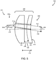
- diagram 500 illustrates transmission of light through at least one embodiment of the pancake lens assembly 206.
- the incoming display light 224 includes the emission profile 308a emitted by the PEC 204 at the distance 304a from the optical axis 210.
- the emission profile 308a may be determined as a function of the distance 304a and the optics of the pancake lens assembly 206, and thus may be different from the emission profile 308b illustrated in FIG. 4 .
- FIG. 5 illustrates two rays 502, 504 that correspond to the beam width 310a of the emission profile 308a. As shown, the rays 502, 504 enter the front of the beam splitter lens 402 and are partially transmitted through the lens 402.
- the rays 502, 504 may also be partially reflected by the beam splitter lens 402 and lost, which is not shown in the diagram 500.
- the rays 502, 504 are transmitted through the beam splitter lens 402 and are next reflected by the front surface of the reflective polarizer lens 404.
- the quarter wave plate 408 of the reflective polarizer lens 404 changes the phase of the rays 502, 504, for example changing the rays 502, 504 from circularly polarized to linearly polarized.
- the rays 502, 504 are transmitted back through the beam splitter lens 402 and then reflected by the front surface of the beam splitter lens 402.
- the reflected rays 502, 504 are next transmitted through the reflective polarizer lens 404 to the eye box 208.
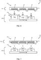
- diagram 600 shows least one embodiment of the display screen 202 and the PEC 204.
- the illustrative display screen 202 is a micro OLED display with a size of less than one inch across and a pixel density of greater than 3000 pixels per inch.
- the display screen 202 includes a substrate 602 coupled to multiple OLED subpixels 604.
- the diagram 600 illustrates three subpixels 604 (red, green, and blue); of course, the display screen 202 includes many more subpixels 604.
- Each of the subpixels 604 includes a resonant cavity 606.
- An LED subpixel 604 without a resonant cavity may have a Lambertian or near-Lambertian emission profile.
- Light may reflect within each resonant cavity 606 multiple times, causing the spectra and emission profile of the emitted light 222 to narrow considerably.
- the spectral and angular emission may be further refined to a very narrow range.
- the illustrative PEC 204 includes a micro prism array 608 for each of the subpixels 604.
- the micro prism array 608 may be embodied as an integrated directional optical film including micro-prism arrays, grating elements, metasurface beam deflector or other directional component.
- the size of each prism element of the micro prism array 608 may be small enough so that it cannot be resolved by the magnifying power of the pancake lens 206.
- the micro prism arrays 608 are included in a glass cover 610. As shown, the micro prism array 608 may change the beam angle (direction) of the transmitted light 224. As described above in connection with FIGS. 4-5 , the direction of each micro-prism array 608 may depend on the relative position of the corresponding subpixel 604 with respect to the pancake lens assembly 206.
- diagram 700 shows least one embodiment of the display screen 202 and the PEC 204.
- the illustrative display screen 202 of FIG. 7 is a micro OLED display with a size of less than one inch across and a pixel density of greater than 3000 pixels per inch.
- the display screen 202 includes a substrate 702 coupled to multiple OLED subpixels 704.
- the diagram 700 illustrates three subpixels 704 (red, green, and blue); of course, the display screen 202 includes many more subpixels 704.
- Each of the subpixels 704 does not include a resonant cavity and thus the emitted light 222 has a Lambertian or near-Lambertian emission profile.
- the illustrative PEC 204 includes a micro lens array 706 and a micro prism array 708 for each of the subpixels 704.
- the micro prism array 708 may be embodied as an integrated directional optical film including micro-prism arrays, grating elements, or other directional component. As described above, the size of each prism element of the micro prism array 608 may be small enough so that it cannot be resolved by the magnifying power of the pancake lens 206.
- the micro lens array 706 and the micro prism array 708 are included in a layer 710, which may be embodied as a single layer with integrated micro lens array 706 and micro prism array 708, or as multiple layers, for example a separate micro lens array 706 layer and a micro prism array 708 layer.
- the display 202 further includes a polarizing layer 808, which is aligned with the polarization of the quantum rod film 804. It should be understood that although illustrated as including both a quantum rod film 804 and a polarizing layer 808, in some embodiments the display 202 may omit the polarizing layer 808 or use the quantum rod film as the polarizing layer 808. By emitting polarized light 806 by the backlight 802, the system 100 may reduce polarization losses in the LCD display 202 and reduce power consumption.
- the display 202 further includes multiple liquid crystal cells 810 and color filters 812.
- the liquid crystal cells 810 may be considerably thin for improved response time. Typically, reducing liquid crystal cell gap reduces power efficiency for LCDs. However, due to the overall improved efficiency of the system 100, overall power consumption may be reduced by two to three times, even with the use of small liquid crystal cells with fast response times.
- the display 202 further includes a polarizing layer 814, which is illustratively aligned perpendicular to the quantum rod film 804 and the polarizing layer 808. Additionally or alternatively, in some embodiments the display 202 may operate in a normally white mode, in which the polarizing layer 814 is aligned parallel to the quantum rod film 804 and the polarizing layer 808.
- the liquid crystal cells 810 are configured to selectively change the polarization angle of the light 806 emitted by the backlight 802, which selectively allows light to pass through the associated color filter 812 and be emitted from the display 202 as the light 222.
- the light 222 may be emitted with a Lambertian, near-Lambertian, or other relatively broad emission profile.
- the polarizing layer 814 may be topped with a quarter wave film so that the light 222 is circularly polarized.
- the illustrative PEC 204 includes a micro lens array 816 and a micro prism array 818 for each of the liquid crystal cells 810.
- the micro prism array 818 may be embodied as an integrated directional optical film including micro-prism arrays, grating elements, or other directional component.
- the micro lens arrays 816 and the micro prism arrays 818 may be included in multiple layers 820. Additionally or alternatively, in some embodiments the PEC 204 may include multiple layers of meta-surface that function as collimator and deflector.
- the micro lens arrays 816 collimate the light emitted by the display 202, narrowing the emission profile (beam width) of each pixel of the emitted light 224.
- the micro prism array 818 may change the beam angle (direction) of the transmitted light 224. As described above in connection with FIGS. 4-5 , the beam width of each micro lens array 816 and the direction of each micro prism array 818 may depend on the relative position of the corresponding liquid crystal cell 810 with respect to the pancake lens assembly 206.
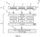
- diagram 900 shows least one embodiment of the display screen 202 and the PEC 204.
- the illustrative display screen 202 of FIG. 9 is a micro LCD display with a relatively high pixel density.
- the display screen 202 includes a backlight 902 coupled to a highly directional coupler 904.
- Typical LCD backlights used, for example, in televisions, smart phones, computer screens, or other directly viewed devices may use a wide angle coupler that disperses the backlight output broadly, in order to produce wide viewing angles.
- the highly directional coupler 904 produces light 906 with a narrow emission profile.
- the emission profile of the light 906 may be much narrower than a Lambertian profile.
- the display 202 further includes a polarizing layer 908 that linearly polarizes the light 906 emitted by the highly directional coupler 904.
- the display 202 further includes multiple liquid crystal cells 910 and color filters 912.
- the liquid crystal cells 910 may be small for improved response time. Typically, reducing liquid crystal cell size reduces power efficiency for LCDs. However, due to the overall improved efficiency of the system 100, overall power consumption may be reduced by two to three times, even with the use of small liquid crystal cells with fast response times.
- the display 202 further includes a polarizing layer 914, which is aligned perpendicular to the polarizing layer 908.
- the liquid crystal cells 910 are configured to selectively change the polarization angle of the light 906 passed through the polarizing layer 908, which selectively allows light to pass through the associated color filter 912 and be emitted from the display 202 as the light 222.
- the light 222 has a narrow emission profile.
- the polarizing layer 914 may be topped with a quarter wave film so that the light 222 is circularly polarized.
- the illustrative PEC 204 includes a micro prism array 916 for each of the liquid crystal cells 910.
- the micro prism array 916 may be embodied as an integrated directional optical film including micro-prism arrays, grating elements, or other directional component.
- the micro prism arrays 916 are included in a glass cover 918. As shown, the micro prism array 916 may change the beam angle (direction) of the transmitted light 224. As described above in connection with FIGS. 4-5 , the direction of each micro prism array 916 may depend on the relative position of the corresponding liquid crystal cell 910 with respect to the pancake lens assembly 206.
- An embodiment of the technologies disclosed herein may include any one or more, and any combination of, the examples described below.
Landscapes
- Physics & Mathematics (AREA)
- General Physics & Mathematics (AREA)
- Optics & Photonics (AREA)
Applications Claiming Priority (1)
| Application Number | Priority Date | Filing Date | Title |
|---|---|---|---|
| US15/935,009 US10712569B2 (en) | 2018-03-25 | 2018-03-25 | Technologies for efficient head-mounted display with pancake lenses |
Publications (2)
| Publication Number | Publication Date |
|---|---|
| EP3547005A1 true EP3547005A1 (de) | 2019-10-02 |
| EP3547005B1 EP3547005B1 (de) | 2024-07-31 |
Family
ID=65275061
Family Applications (1)
| Application Number | Title | Priority Date | Filing Date |
|---|---|---|---|
| EP19157039.9A Active EP3547005B1 (de) | 2018-03-25 | 2019-02-13 | Technologien für eine effiziente kopfmontierte anzeige mit pancake-objektiv |
Country Status (4)
| Country | Link |
|---|---|
| US (1) | US10712569B2 (de) |
| EP (1) | EP3547005B1 (de) |
| KR (1) | KR102774813B1 (de) |
| CN (1) | CN110308554A (de) |
Families Citing this family (18)
| Publication number | Priority date | Publication date | Assignee | Title |
|---|---|---|---|---|
| CN107861247B (zh) * | 2017-12-22 | 2020-08-25 | 联想(北京)有限公司 | 光学部件及增强现实设备 |
| DE102018121258A1 (de) * | 2018-08-30 | 2020-03-05 | Vr Coaster Gmbh & Co. Kg | Head Mounted Display sowie Vergnügungseinrichtung mit einem solchen Head Mounted Display |
| US10825370B1 (en) * | 2018-10-30 | 2020-11-03 | Facebook Technologies, Llc | Systems and methods for updating pixel arrays |
| US11552163B2 (en) * | 2019-02-22 | 2023-01-10 | Vuereal Inc. | Staggered and tile stacked microdevice integration and driving |
| KR102642698B1 (ko) * | 2019-04-30 | 2024-03-04 | 레이아 인코포레이티드 | 이분 방출 패턴을 갖는 광원, 멀티뷰 백라이트 및 방법 |
| US10955675B1 (en) * | 2019-04-30 | 2021-03-23 | Facebook Technologies, Llc | Variable resolution display device with switchable window and see-through pancake lens assembly |
| US11842989B2 (en) * | 2020-03-10 | 2023-12-12 | Meta Platforms Technologies, Llc | Integrating control circuits with light emissive circuits with dissimilar wafer sizes |
| CN212111989U (zh) * | 2020-05-27 | 2020-12-08 | 歌尔光学科技有限公司 | 光学系统及虚拟现实设备 |
| CN111736350A (zh) | 2020-08-02 | 2020-10-02 | 关春东 | 一种近眼显示装置 |
| EP4071541B1 (de) * | 2021-04-07 | 2024-03-06 | Yazaki Corporation | Fahrzeuganzeigevorrichtung |
| US12204096B2 (en) | 2021-06-07 | 2025-01-21 | Panamorph, Inc. | Near-eye display system |
| WO2022170287A2 (en) | 2021-06-07 | 2022-08-11 | Panamorph, Inc. | Near-eye display system |
| US11899209B2 (en) * | 2021-12-17 | 2024-02-13 | Inseye Inc. | Eye tracking system for VR/AR HMD units including pancake lens modules |
| WO2023164131A1 (en) * | 2022-02-25 | 2023-08-31 | Meta Platforms Technologies, Llc | Efficient pancake lens for peripheral view in virtual reality headsets |
| CN116974068A (zh) * | 2022-04-21 | 2023-10-31 | 深圳市Tcl高新技术开发有限公司 | 光学模组、光学系统及显示设备 |
| WO2024018339A1 (en) * | 2022-07-21 | 2024-01-25 | 3M Innovative Properties Company | Display and display system |
| TWI838140B (zh) * | 2023-02-24 | 2024-04-01 | 新鉅科技股份有限公司 | 光學透鏡組及頭戴式電子裝置 |
| WO2025072070A1 (en) * | 2023-09-28 | 2025-04-03 | Meta Platforms Technologies, Llc | Virtual reality display sun damage mitigation |
Citations (4)
| Publication number | Priority date | Publication date | Assignee | Title |
|---|---|---|---|---|
| EP1357417A2 (de) * | 2002-04-24 | 2003-10-29 | Seos Limited | Okular zum Betrachten eines flachen Bildes |
| DE69733867T2 (de) * | 1996-03-11 | 2006-04-13 | Seiko Epson Corp. | Am kopf befestigte anzeigevorrichtung |
| US20170255015A1 (en) * | 2016-03-02 | 2017-09-07 | Oculus Vr, Llc | Field curvature corrected display |
| US20170358136A1 (en) * | 2016-06-10 | 2017-12-14 | Oculus Vr, Llc | Focus adjusting virtual reality headset |
Family Cites Families (1)
| Publication number | Priority date | Publication date | Assignee | Title |
|---|---|---|---|---|
| US20040108971A1 (en) * | 1998-04-09 | 2004-06-10 | Digilens, Inc. | Method of and apparatus for viewing an image |
-
2018
- 2018-03-25 US US15/935,009 patent/US10712569B2/en active Active
-
2019
- 2019-02-13 EP EP19157039.9A patent/EP3547005B1/de active Active
- 2019-02-20 KR KR1020190019695A patent/KR102774813B1/ko active Active
- 2019-02-21 CN CN201910129863.1A patent/CN110308554A/zh active Pending
Patent Citations (4)
| Publication number | Priority date | Publication date | Assignee | Title |
|---|---|---|---|---|
| DE69733867T2 (de) * | 1996-03-11 | 2006-04-13 | Seiko Epson Corp. | Am kopf befestigte anzeigevorrichtung |
| EP1357417A2 (de) * | 2002-04-24 | 2003-10-29 | Seos Limited | Okular zum Betrachten eines flachen Bildes |
| US20170255015A1 (en) * | 2016-03-02 | 2017-09-07 | Oculus Vr, Llc | Field curvature corrected display |
| US20170358136A1 (en) * | 2016-06-10 | 2017-12-14 | Oculus Vr, Llc | Focus adjusting virtual reality headset |
Also Published As
| Publication number | Publication date |
|---|---|
| US20190049733A1 (en) | 2019-02-14 |
| KR20190112248A (ko) | 2019-10-04 |
| EP3547005B1 (de) | 2024-07-31 |
| US10712569B2 (en) | 2020-07-14 |
| KR102774813B1 (ko) | 2025-03-04 |
| CN110308554A (zh) | 2019-10-08 |
Similar Documents
| Publication | Publication Date | Title |
|---|---|---|
| EP3547005B1 (de) | Technologien für eine effiziente kopfmontierte anzeige mit pancake-objektiv | |
| US11029523B2 (en) | Near-eye display with self-emitting microdisplay engine | |
| US11385502B1 (en) | Near-eye display apparatus | |
| CN100529837C (zh) | 基片导波的光学装置 | |
| CN104937476B (zh) | 头戴式显示器的光学组合器中的级联光学器件 | |
| US9420266B2 (en) | Stepped waveguide autostereoscopic display apparatus with a reflective directional element | |
| KR102773619B1 (ko) | 협각 백라이트를 갖는 헤드 장착형 디스플레이 | |
| US12399369B2 (en) | Curved light guide image combiner and system including the same | |
| US20220367839A1 (en) | Color conversion display with polarized emission enhancement | |
| CN114488538A (zh) | Ar光机和头戴显示设备 | |
| US20230236396A1 (en) | Compact optics for head-mounted display systems | |
| Li et al. | Front-lit LCOS for AR displays | |
| US20240103312A1 (en) | Compact display engine with arrayed illumination source | |
| US11513357B2 (en) | Image display device for providing uniform brightness in virtual image | |
| US12523907B2 (en) | Wide color gamut enabled edge-lit BLU for high PPI VR-LCD display | |
| US20250208466A1 (en) | Light collimating film for liquid crystal display backlight | |
| US12332519B2 (en) | Backlight unit and color filter on array configuration for a liquid crystal display | |
| US12197074B2 (en) | Display backlight with light expander structures | |
| WO2025137080A1 (en) | Light collimating film for liquid crystal display backlight | |
| CN118818842A (zh) | 用于液晶显示器的背光单元和阵列上滤色器配置 | |
| WO2025007092A1 (en) | Image light guide projector system alignment | |
| CN118642291A (zh) | 用于高ppi vr-lcd显示器的实现广色域的侧光式blu |
Legal Events
| Date | Code | Title | Description |
|---|---|---|---|
| PUAI | Public reference made under article 153(3) epc to a published international application that has entered the european phase |
Free format text: ORIGINAL CODE: 0009012 |
|
| STAA | Information on the status of an ep patent application or granted ep patent |
Free format text: STATUS: THE APPLICATION HAS BEEN PUBLISHED |
|
| AK | Designated contracting states |
Kind code of ref document: A1 Designated state(s): AL AT BE BG CH CY CZ DE DK EE ES FI FR GB GR HR HU IE IS IT LI LT LU LV MC MK MT NL NO PL PT RO RS SE SI SK SM TR |
|
| AX | Request for extension of the european patent |
Extension state: BA ME |
|
| STAA | Information on the status of an ep patent application or granted ep patent |
Free format text: STATUS: REQUEST FOR EXAMINATION WAS MADE |
|
| 17P | Request for examination filed |
Effective date: 20200402 |
|
| RBV | Designated contracting states (corrected) |
Designated state(s): AL AT BE BG CH CY CZ DE DK EE ES FI FR GB GR HR HU IE IS IT LI LT LU LV MC MK MT NL NO PL PT RO RS SE SI SK SM TR |
|
| STAA | Information on the status of an ep patent application or granted ep patent |
Free format text: STATUS: EXAMINATION IS IN PROGRESS |
|
| 17Q | First examination report despatched |
Effective date: 20220429 |
|
| GRAP | Despatch of communication of intention to grant a patent |
Free format text: ORIGINAL CODE: EPIDOSNIGR1 |
|
| STAA | Information on the status of an ep patent application or granted ep patent |
Free format text: STATUS: GRANT OF PATENT IS INTENDED |
|
| INTG | Intention to grant announced |
Effective date: 20240228 |
|
| GRAS | Grant fee paid |
Free format text: ORIGINAL CODE: EPIDOSNIGR3 |
|
| GRAA | (expected) grant |
Free format text: ORIGINAL CODE: 0009210 |
|
| STAA | Information on the status of an ep patent application or granted ep patent |
Free format text: STATUS: THE PATENT HAS BEEN GRANTED |
|
| AK | Designated contracting states |
Kind code of ref document: B1 Designated state(s): AL AT BE BG CH CY CZ DE DK EE ES FI FR GB GR HR HU IE IS IT LI LT LU LV MC MK MT NL NO PL PT RO RS SE SI SK SM TR |
|
| REG | Reference to a national code |
Ref country code: CH Ref legal event code: EP Ref country code: GB Ref legal event code: FG4D |
|
| REG | Reference to a national code |
Ref country code: DE Ref legal event code: R096 Ref document number: 602019055980 Country of ref document: DE |
|
| P01 | Opt-out of the competence of the unified patent court (upc) registered |
Free format text: CASE NUMBER: APP_42981/2024 Effective date: 20240722 |
|
| REG | Reference to a national code |
Ref country code: IE Ref legal event code: FG4D |
|
| REG | Reference to a national code |
Ref country code: NL Ref legal event code: FP |
|
| REG | Reference to a national code |
Ref country code: LT Ref legal event code: MG9D |
|
| PG25 | Lapsed in a contracting state [announced via postgrant information from national office to epo] |
Ref country code: PT Free format text: LAPSE BECAUSE OF FAILURE TO SUBMIT A TRANSLATION OF THE DESCRIPTION OR TO PAY THE FEE WITHIN THE PRESCRIBED TIME-LIMIT Effective date: 20241202 |
|
| REG | Reference to a national code |
Ref country code: AT Ref legal event code: MK05 Ref document number: 1709019 Country of ref document: AT Kind code of ref document: T Effective date: 20240731 |
|
| PG25 | Lapsed in a contracting state [announced via postgrant information from national office to epo] |
Ref country code: PT Free format text: LAPSE BECAUSE OF FAILURE TO SUBMIT A TRANSLATION OF THE DESCRIPTION OR TO PAY THE FEE WITHIN THE PRESCRIBED TIME-LIMIT Effective date: 20241202 |
|
| PG25 | Lapsed in a contracting state [announced via postgrant information from national office to epo] |
Ref country code: NO Free format text: LAPSE BECAUSE OF FAILURE TO SUBMIT A TRANSLATION OF THE DESCRIPTION OR TO PAY THE FEE WITHIN THE PRESCRIBED TIME-LIMIT Effective date: 20241031 |
|
| PG25 | Lapsed in a contracting state [announced via postgrant information from national office to epo] |
Ref country code: PL Free format text: LAPSE BECAUSE OF FAILURE TO SUBMIT A TRANSLATION OF THE DESCRIPTION OR TO PAY THE FEE WITHIN THE PRESCRIBED TIME-LIMIT Effective date: 20240731 Ref country code: GR Free format text: LAPSE BECAUSE OF FAILURE TO SUBMIT A TRANSLATION OF THE DESCRIPTION OR TO PAY THE FEE WITHIN THE PRESCRIBED TIME-LIMIT Effective date: 20241101 Ref country code: FI Free format text: LAPSE BECAUSE OF FAILURE TO SUBMIT A TRANSLATION OF THE DESCRIPTION OR TO PAY THE FEE WITHIN THE PRESCRIBED TIME-LIMIT Effective date: 20240731 |
|
| PGFP | Annual fee paid to national office [announced via postgrant information from national office to epo] |
Ref country code: NL Payment date: 20241203 Year of fee payment: 7 |
|
| PG25 | Lapsed in a contracting state [announced via postgrant information from national office to epo] |
Ref country code: BG Free format text: LAPSE BECAUSE OF FAILURE TO SUBMIT A TRANSLATION OF THE DESCRIPTION OR TO PAY THE FEE WITHIN THE PRESCRIBED TIME-LIMIT Effective date: 20240731 |
|
| PG25 | Lapsed in a contracting state [announced via postgrant information from national office to epo] |
Ref country code: LV Free format text: LAPSE BECAUSE OF FAILURE TO SUBMIT A TRANSLATION OF THE DESCRIPTION OR TO PAY THE FEE WITHIN THE PRESCRIBED TIME-LIMIT Effective date: 20240731 |
|
| PG25 | Lapsed in a contracting state [announced via postgrant information from national office to epo] |
Ref country code: AT Free format text: LAPSE BECAUSE OF FAILURE TO SUBMIT A TRANSLATION OF THE DESCRIPTION OR TO PAY THE FEE WITHIN THE PRESCRIBED TIME-LIMIT Effective date: 20240731 Ref country code: IS Free format text: LAPSE BECAUSE OF FAILURE TO SUBMIT A TRANSLATION OF THE DESCRIPTION OR TO PAY THE FEE WITHIN THE PRESCRIBED TIME-LIMIT Effective date: 20241130 |
|
| PG25 | Lapsed in a contracting state [announced via postgrant information from national office to epo] |
Ref country code: HR Free format text: LAPSE BECAUSE OF FAILURE TO SUBMIT A TRANSLATION OF THE DESCRIPTION OR TO PAY THE FEE WITHIN THE PRESCRIBED TIME-LIMIT Effective date: 20240731 |
|
| PG25 | Lapsed in a contracting state [announced via postgrant information from national office to epo] |
Ref country code: ES Free format text: LAPSE BECAUSE OF FAILURE TO SUBMIT A TRANSLATION OF THE DESCRIPTION OR TO PAY THE FEE WITHIN THE PRESCRIBED TIME-LIMIT Effective date: 20240731 Ref country code: RS Free format text: LAPSE BECAUSE OF FAILURE TO SUBMIT A TRANSLATION OF THE DESCRIPTION OR TO PAY THE FEE WITHIN THE PRESCRIBED TIME-LIMIT Effective date: 20241031 |
|
| PG25 | Lapsed in a contracting state [announced via postgrant information from national office to epo] |
Ref country code: RS Free format text: LAPSE BECAUSE OF FAILURE TO SUBMIT A TRANSLATION OF THE DESCRIPTION OR TO PAY THE FEE WITHIN THE PRESCRIBED TIME-LIMIT Effective date: 20241031 Ref country code: PL Free format text: LAPSE BECAUSE OF FAILURE TO SUBMIT A TRANSLATION OF THE DESCRIPTION OR TO PAY THE FEE WITHIN THE PRESCRIBED TIME-LIMIT Effective date: 20240731 Ref country code: NO Free format text: LAPSE BECAUSE OF FAILURE TO SUBMIT A TRANSLATION OF THE DESCRIPTION OR TO PAY THE FEE WITHIN THE PRESCRIBED TIME-LIMIT Effective date: 20241031 Ref country code: LV Free format text: LAPSE BECAUSE OF FAILURE TO SUBMIT A TRANSLATION OF THE DESCRIPTION OR TO PAY THE FEE WITHIN THE PRESCRIBED TIME-LIMIT Effective date: 20240731 Ref country code: IS Free format text: LAPSE BECAUSE OF FAILURE TO SUBMIT A TRANSLATION OF THE DESCRIPTION OR TO PAY THE FEE WITHIN THE PRESCRIBED TIME-LIMIT Effective date: 20241130 Ref country code: HR Free format text: LAPSE BECAUSE OF FAILURE TO SUBMIT A TRANSLATION OF THE DESCRIPTION OR TO PAY THE FEE WITHIN THE PRESCRIBED TIME-LIMIT Effective date: 20240731 Ref country code: GR Free format text: LAPSE BECAUSE OF FAILURE TO SUBMIT A TRANSLATION OF THE DESCRIPTION OR TO PAY THE FEE WITHIN THE PRESCRIBED TIME-LIMIT Effective date: 20241101 Ref country code: FI Free format text: LAPSE BECAUSE OF FAILURE TO SUBMIT A TRANSLATION OF THE DESCRIPTION OR TO PAY THE FEE WITHIN THE PRESCRIBED TIME-LIMIT Effective date: 20240731 Ref country code: ES Free format text: LAPSE BECAUSE OF FAILURE TO SUBMIT A TRANSLATION OF THE DESCRIPTION OR TO PAY THE FEE WITHIN THE PRESCRIBED TIME-LIMIT Effective date: 20240731 Ref country code: BG Free format text: LAPSE BECAUSE OF FAILURE TO SUBMIT A TRANSLATION OF THE DESCRIPTION OR TO PAY THE FEE WITHIN THE PRESCRIBED TIME-LIMIT Effective date: 20240731 Ref country code: AT Free format text: LAPSE BECAUSE OF FAILURE TO SUBMIT A TRANSLATION OF THE DESCRIPTION OR TO PAY THE FEE WITHIN THE PRESCRIBED TIME-LIMIT Effective date: 20240731 |
|
| PGFP | Annual fee paid to national office [announced via postgrant information from national office to epo] |
Ref country code: DE Payment date: 20250121 Year of fee payment: 7 |
|
| PG25 | Lapsed in a contracting state [announced via postgrant information from national office to epo] |
Ref country code: DK Free format text: LAPSE BECAUSE OF FAILURE TO SUBMIT A TRANSLATION OF THE DESCRIPTION OR TO PAY THE FEE WITHIN THE PRESCRIBED TIME-LIMIT Effective date: 20240731 Ref country code: RO Free format text: LAPSE BECAUSE OF FAILURE TO SUBMIT A TRANSLATION OF THE DESCRIPTION OR TO PAY THE FEE WITHIN THE PRESCRIBED TIME-LIMIT Effective date: 20240731 Ref country code: SM Free format text: LAPSE BECAUSE OF FAILURE TO SUBMIT A TRANSLATION OF THE DESCRIPTION OR TO PAY THE FEE WITHIN THE PRESCRIBED TIME-LIMIT Effective date: 20240731 |
|
| PG25 | Lapsed in a contracting state [announced via postgrant information from national office to epo] |
Ref country code: EE Free format text: LAPSE BECAUSE OF FAILURE TO SUBMIT A TRANSLATION OF THE DESCRIPTION OR TO PAY THE FEE WITHIN THE PRESCRIBED TIME-LIMIT Effective date: 20240731 |
|
| PG25 | Lapsed in a contracting state [announced via postgrant information from national office to epo] |
Ref country code: CZ Free format text: LAPSE BECAUSE OF FAILURE TO SUBMIT A TRANSLATION OF THE DESCRIPTION OR TO PAY THE FEE WITHIN THE PRESCRIBED TIME-LIMIT Effective date: 20240731 |
|
| PG25 | Lapsed in a contracting state [announced via postgrant information from national office to epo] |
Ref country code: SK Free format text: LAPSE BECAUSE OF FAILURE TO SUBMIT A TRANSLATION OF THE DESCRIPTION OR TO PAY THE FEE WITHIN THE PRESCRIBED TIME-LIMIT Effective date: 20240731 Ref country code: IT Free format text: LAPSE BECAUSE OF FAILURE TO SUBMIT A TRANSLATION OF THE DESCRIPTION OR TO PAY THE FEE WITHIN THE PRESCRIBED TIME-LIMIT Effective date: 20240731 |
|
| REG | Reference to a national code |
Ref country code: DE Ref legal event code: R097 Ref document number: 602019055980 Country of ref document: DE |
|
| PLBE | No opposition filed within time limit |
Free format text: ORIGINAL CODE: 0009261 |
|
| STAA | Information on the status of an ep patent application or granted ep patent |
Free format text: STATUS: NO OPPOSITION FILED WITHIN TIME LIMIT |
|
| 26N | No opposition filed |
Effective date: 20250501 |
|
| PG25 | Lapsed in a contracting state [announced via postgrant information from national office to epo] |
Ref country code: SE Free format text: LAPSE BECAUSE OF FAILURE TO SUBMIT A TRANSLATION OF THE DESCRIPTION OR TO PAY THE FEE WITHIN THE PRESCRIBED TIME-LIMIT Effective date: 20240731 |
|
| PG25 | Lapsed in a contracting state [announced via postgrant information from national office to epo] |
Ref country code: MC Free format text: LAPSE BECAUSE OF FAILURE TO SUBMIT A TRANSLATION OF THE DESCRIPTION OR TO PAY THE FEE WITHIN THE PRESCRIBED TIME-LIMIT Effective date: 20240731 |
|
| REG | Reference to a national code |
Ref country code: CH Ref legal event code: PL |
|
| PG25 | Lapsed in a contracting state [announced via postgrant information from national office to epo] |
Ref country code: LU Free format text: LAPSE BECAUSE OF NON-PAYMENT OF DUE FEES Effective date: 20250213 |
|
| PG25 | Lapsed in a contracting state [announced via postgrant information from national office to epo] |
Ref country code: CH Free format text: LAPSE BECAUSE OF NON-PAYMENT OF DUE FEES Effective date: 20250228 |
|
| GBPC | Gb: european patent ceased through non-payment of renewal fee |
Effective date: 20250213 |
|
| REG | Reference to a national code |
Ref country code: BE Ref legal event code: MM Effective date: 20250228 |
|
| PG25 | Lapsed in a contracting state [announced via postgrant information from national office to epo] |
Ref country code: GB Free format text: LAPSE BECAUSE OF NON-PAYMENT OF DUE FEES Effective date: 20250213 |
|
| PG25 | Lapsed in a contracting state [announced via postgrant information from national office to epo] |
Ref country code: FR Free format text: LAPSE BECAUSE OF NON-PAYMENT OF DUE FEES Effective date: 20250228 |
|
| PG25 | Lapsed in a contracting state [announced via postgrant information from national office to epo] |
Ref country code: BE Free format text: LAPSE BECAUSE OF NON-PAYMENT OF DUE FEES Effective date: 20250228 |
|
| PG25 | Lapsed in a contracting state [announced via postgrant information from national office to epo] |
Ref country code: IE Free format text: LAPSE BECAUSE OF NON-PAYMENT OF DUE FEES Effective date: 20250213 |