EP3542948A1 - Display device - Google Patents
Display device Download PDFInfo
- Publication number
- EP3542948A1 EP3542948A1 EP19162851.0A EP19162851A EP3542948A1 EP 3542948 A1 EP3542948 A1 EP 3542948A1 EP 19162851 A EP19162851 A EP 19162851A EP 3542948 A1 EP3542948 A1 EP 3542948A1
- Authority
- EP
- European Patent Office
- Prior art keywords
- pad
- connecting post
- metal line
- substrate
- display device
- Prior art date
- Legal status (The legal status is an assumption and is not a legal conclusion. Google has not performed a legal analysis and makes no representation as to the accuracy of the status listed.)
- Pending
Links
Images






Classifications
-
- B—PERFORMING OPERATIONS; TRANSPORTING
- B23—MACHINE TOOLS; METAL-WORKING NOT OTHERWISE PROVIDED FOR
- B23K—SOLDERING OR UNSOLDERING; WELDING; CLADDING OR PLATING BY SOLDERING OR WELDING; CUTTING BY APPLYING HEAT LOCALLY, e.g. FLAME CUTTING; WORKING BY LASER BEAM
- B23K35/00—Rods, electrodes, materials, or media, for use in soldering, welding, or cutting
- B23K35/22—Rods, electrodes, materials, or media, for use in soldering, welding, or cutting characterised by the composition or nature of the material
- B23K35/24—Selection of soldering or welding materials proper
- B23K35/26—Selection of soldering or welding materials proper with the principal constituent melting at less than 400°C
- B23K35/262—Sn as the principal constituent
-
- H—ELECTRICITY
- H10—SEMICONDUCTOR DEVICES; ELECTRIC SOLID-STATE DEVICES NOT OTHERWISE PROVIDED FOR
- H10W—GENERIC PACKAGES, INTERCONNECTIONS, CONNECTORS OR OTHER CONSTRUCTIONAL DETAILS OF DEVICES COVERED BY CLASS H10
- H10W90/00—Package configurations
- H10W90/701—Package configurations characterised by the relative positions of pads or connectors relative to package parts
-
- H—ELECTRICITY
- H10—SEMICONDUCTOR DEVICES; ELECTRIC SOLID-STATE DEVICES NOT OTHERWISE PROVIDED FOR
- H10H—INORGANIC LIGHT-EMITTING SEMICONDUCTOR DEVICES HAVING POTENTIAL BARRIERS
- H10H29/00—Integrated devices, or assemblies of multiple devices, comprising at least one light-emitting semiconductor element covered by group H10H20/00
- H10H29/10—Integrated devices comprising at least one light-emitting semiconductor component covered by group H10H20/00
- H10H29/14—Integrated devices comprising at least one light-emitting semiconductor component covered by group H10H20/00 comprising multiple light-emitting semiconductor components
- H10H29/142—Two-dimensional arrangements, e.g. asymmetric LED layout
-
- B—PERFORMING OPERATIONS; TRANSPORTING
- B23—MACHINE TOOLS; METAL-WORKING NOT OTHERWISE PROVIDED FOR
- B23K—SOLDERING OR UNSOLDERING; WELDING; CLADDING OR PLATING BY SOLDERING OR WELDING; CUTTING BY APPLYING HEAT LOCALLY, e.g. FLAME CUTTING; WORKING BY LASER BEAM
- B23K35/00—Rods, electrodes, materials, or media, for use in soldering, welding, or cutting
- B23K35/22—Rods, electrodes, materials, or media, for use in soldering, welding, or cutting characterised by the composition or nature of the material
- B23K35/24—Selection of soldering or welding materials proper
- B23K35/30—Selection of soldering or welding materials proper with the principal constituent melting at less than 1550°C
-
- B—PERFORMING OPERATIONS; TRANSPORTING
- B23—MACHINE TOOLS; METAL-WORKING NOT OTHERWISE PROVIDED FOR
- B23K—SOLDERING OR UNSOLDERING; WELDING; CLADDING OR PLATING BY SOLDERING OR WELDING; CUTTING BY APPLYING HEAT LOCALLY, e.g. FLAME CUTTING; WORKING BY LASER BEAM
- B23K35/00—Rods, electrodes, materials, or media, for use in soldering, welding, or cutting
- B23K35/22—Rods, electrodes, materials, or media, for use in soldering, welding, or cutting characterised by the composition or nature of the material
- B23K35/24—Selection of soldering or welding materials proper
- B23K35/32—Selection of soldering or welding materials proper with the principal constituent melting at more than 1550°C
-
- H—ELECTRICITY
- H05—ELECTRIC TECHNIQUES NOT OTHERWISE PROVIDED FOR
- H05K—PRINTED CIRCUITS; CASINGS OR CONSTRUCTIONAL DETAILS OF ELECTRIC APPARATUS; MANUFACTURE OF ASSEMBLAGES OF ELECTRICAL COMPONENTS
- H05K1/00—Printed circuits
- H05K1/02—Details
- H05K1/0296—Conductive pattern lay-out details not covered by sub groups H05K1/02 - H05K1/0295
-
- H—ELECTRICITY
- H05—ELECTRIC TECHNIQUES NOT OTHERWISE PROVIDED FOR
- H05K—PRINTED CIRCUITS; CASINGS OR CONSTRUCTIONAL DETAILS OF ELECTRIC APPARATUS; MANUFACTURE OF ASSEMBLAGES OF ELECTRICAL COMPONENTS
- H05K1/00—Printed circuits
- H05K1/18—Printed circuits structurally associated with non-printed electric components
- H05K1/181—Printed circuits structurally associated with non-printed electric components associated with surface mounted components
-
- H—ELECTRICITY
- H10—SEMICONDUCTOR DEVICES; ELECTRIC SOLID-STATE DEVICES NOT OTHERWISE PROVIDED FOR
- H10D—INORGANIC ELECTRIC SEMICONDUCTOR DEVICES
- H10D86/00—Integrated devices formed in or on insulating or conducting substrates, e.g. formed in silicon-on-insulator [SOI] substrates or on stainless steel or glass substrates
- H10D86/40—Integrated devices formed in or on insulating or conducting substrates, e.g. formed in silicon-on-insulator [SOI] substrates or on stainless steel or glass substrates characterised by multiple TFTs
- H10D86/441—Interconnections, e.g. scanning lines
-
- H—ELECTRICITY
- H10—SEMICONDUCTOR DEVICES; ELECTRIC SOLID-STATE DEVICES NOT OTHERWISE PROVIDED FOR
- H10D—INORGANIC ELECTRIC SEMICONDUCTOR DEVICES
- H10D86/00—Integrated devices formed in or on insulating or conducting substrates, e.g. formed in silicon-on-insulator [SOI] substrates or on stainless steel or glass substrates
- H10D86/40—Integrated devices formed in or on insulating or conducting substrates, e.g. formed in silicon-on-insulator [SOI] substrates or on stainless steel or glass substrates characterised by multiple TFTs
- H10D86/60—Integrated devices formed in or on insulating or conducting substrates, e.g. formed in silicon-on-insulator [SOI] substrates or on stainless steel or glass substrates characterised by multiple TFTs wherein the TFTs are in active matrices
-
- H—ELECTRICITY
- H10—SEMICONDUCTOR DEVICES; ELECTRIC SOLID-STATE DEVICES NOT OTHERWISE PROVIDED FOR
- H10F—INORGANIC SEMICONDUCTOR DEVICES SENSITIVE TO INFRARED RADIATION, LIGHT, ELECTROMAGNETIC RADIATION OF SHORTER WAVELENGTH OR CORPUSCULAR RADIATION
- H10F39/00—Integrated devices, or assemblies of multiple devices, comprising at least one element covered by group H10F30/00, e.g. radiation detectors comprising photodiode arrays
- H10F39/10—Integrated devices
- H10F39/103—Integrated devices the at least one element covered by H10F30/00 having potential barriers, e.g. integrated devices comprising photodiodes or phototransistors
-
- H—ELECTRICITY
- H10—SEMICONDUCTOR DEVICES; ELECTRIC SOLID-STATE DEVICES NOT OTHERWISE PROVIDED FOR
- H10H—INORGANIC LIGHT-EMITTING SEMICONDUCTOR DEVICES HAVING POTENTIAL BARRIERS
- H10H20/00—Individual inorganic light-emitting semiconductor devices having potential barriers, e.g. light-emitting diodes [LED]
- H10H20/01—Manufacture or treatment
- H10H20/011—Manufacture or treatment of bodies, e.g. forming semiconductor layers
- H10H20/018—Bonding of wafers
-
- H—ELECTRICITY
- H10—SEMICONDUCTOR DEVICES; ELECTRIC SOLID-STATE DEVICES NOT OTHERWISE PROVIDED FOR
- H10H—INORGANIC LIGHT-EMITTING SEMICONDUCTOR DEVICES HAVING POTENTIAL BARRIERS
- H10H20/00—Individual inorganic light-emitting semiconductor devices having potential barriers, e.g. light-emitting diodes [LED]
- H10H20/80—Constructional details
- H10H20/85—Packages
- H10H20/857—Interconnections, e.g. lead-frames, bond wires or solder balls
-
- H—ELECTRICITY
- H10—SEMICONDUCTOR DEVICES; ELECTRIC SOLID-STATE DEVICES NOT OTHERWISE PROVIDED FOR
- H10W—GENERIC PACKAGES, INTERCONNECTIONS, CONNECTORS OR OTHER CONSTRUCTIONAL DETAILS OF DEVICES COVERED BY CLASS H10
- H10W70/00—Package substrates; Interposers; Redistribution layers [RDL]
- H10W70/01—Manufacture or treatment
- H10W70/05—Manufacture or treatment of insulating or insulated package substrates, or of interposers, or of redistribution layers
- H10W70/08—Manufacture or treatment of insulating or insulated package substrates, or of interposers, or of redistribution layers by depositing layers on the chip or wafer, e.g. "chip-first" RDLs
- H10W70/09—Manufacture or treatment of insulating or insulated package substrates, or of interposers, or of redistribution layers by depositing layers on the chip or wafer, e.g. "chip-first" RDLs extending onto an encapsulation that laterally surrounds the chip or wafer, e.g. fan-out wafer level package [FOWLP] RDLs
-
- H—ELECTRICITY
- H10—SEMICONDUCTOR DEVICES; ELECTRIC SOLID-STATE DEVICES NOT OTHERWISE PROVIDED FOR
- H10W—GENERIC PACKAGES, INTERCONNECTIONS, CONNECTORS OR OTHER CONSTRUCTIONAL DETAILS OF DEVICES COVERED BY CLASS H10
- H10W70/00—Package substrates; Interposers; Redistribution layers [RDL]
- H10W70/60—Insulating or insulated package substrates; Interposers; Redistribution layers
-
- H—ELECTRICITY
- H10—SEMICONDUCTOR DEVICES; ELECTRIC SOLID-STATE DEVICES NOT OTHERWISE PROVIDED FOR
- H10W—GENERIC PACKAGES, INTERCONNECTIONS, CONNECTORS OR OTHER CONSTRUCTIONAL DETAILS OF DEVICES COVERED BY CLASS H10
- H10W70/00—Package substrates; Interposers; Redistribution layers [RDL]
- H10W70/60—Insulating or insulated package substrates; Interposers; Redistribution layers
- H10W70/62—Insulating or insulated package substrates; Interposers; Redistribution layers characterised by their interconnections
- H10W70/65—Shapes or dispositions of interconnections
-
- H—ELECTRICITY
- H10—SEMICONDUCTOR DEVICES; ELECTRIC SOLID-STATE DEVICES NOT OTHERWISE PROVIDED FOR
- H10W—GENERIC PACKAGES, INTERCONNECTIONS, CONNECTORS OR OTHER CONSTRUCTIONAL DETAILS OF DEVICES COVERED BY CLASS H10
- H10W72/00—Interconnections or connectors in packages
-
- H—ELECTRICITY
- H10—SEMICONDUCTOR DEVICES; ELECTRIC SOLID-STATE DEVICES NOT OTHERWISE PROVIDED FOR
- H10W—GENERIC PACKAGES, INTERCONNECTIONS, CONNECTORS OR OTHER CONSTRUCTIONAL DETAILS OF DEVICES COVERED BY CLASS H10
- H10W72/00—Interconnections or connectors in packages
- H10W72/01—Manufacture or treatment
- H10W72/012—Manufacture or treatment of bump connectors, dummy bumps or thermal bumps
-
- H—ELECTRICITY
- H10—SEMICONDUCTOR DEVICES; ELECTRIC SOLID-STATE DEVICES NOT OTHERWISE PROVIDED FOR
- H10W—GENERIC PACKAGES, INTERCONNECTIONS, CONNECTORS OR OTHER CONSTRUCTIONAL DETAILS OF DEVICES COVERED BY CLASS H10
- H10W72/00—Interconnections or connectors in packages
- H10W72/071—Connecting or disconnecting
- H10W72/072—Connecting or disconnecting of bump connectors
-
- H—ELECTRICITY
- H10—SEMICONDUCTOR DEVICES; ELECTRIC SOLID-STATE DEVICES NOT OTHERWISE PROVIDED FOR
- H10W—GENERIC PACKAGES, INTERCONNECTIONS, CONNECTORS OR OTHER CONSTRUCTIONAL DETAILS OF DEVICES COVERED BY CLASS H10
- H10W72/00—Interconnections or connectors in packages
- H10W72/90—Bond pads, in general
-
- H—ELECTRICITY
- H10—SEMICONDUCTOR DEVICES; ELECTRIC SOLID-STATE DEVICES NOT OTHERWISE PROVIDED FOR
- H10W—GENERIC PACKAGES, INTERCONNECTIONS, CONNECTORS OR OTHER CONSTRUCTIONAL DETAILS OF DEVICES COVERED BY CLASS H10
- H10W72/00—Interconnections or connectors in packages
- H10W72/90—Bond pads, in general
- H10W72/921—Structures or relative sizes of bond pads
- H10W72/923—Bond pads having multiple stacked layers
-
- H—ELECTRICITY
- H10—SEMICONDUCTOR DEVICES; ELECTRIC SOLID-STATE DEVICES NOT OTHERWISE PROVIDED FOR
- H10W—GENERIC PACKAGES, INTERCONNECTIONS, CONNECTORS OR OTHER CONSTRUCTIONAL DETAILS OF DEVICES COVERED BY CLASS H10
- H10W90/00—Package configurations
-
- H—ELECTRICITY
- H10—SEMICONDUCTOR DEVICES; ELECTRIC SOLID-STATE DEVICES NOT OTHERWISE PROVIDED FOR
- H10W—GENERIC PACKAGES, INTERCONNECTIONS, CONNECTORS OR OTHER CONSTRUCTIONAL DETAILS OF DEVICES COVERED BY CLASS H10
- H10W99/00—Subject matter not provided for in other groups of this subclass
-
- B—PERFORMING OPERATIONS; TRANSPORTING
- B23—MACHINE TOOLS; METAL-WORKING NOT OTHERWISE PROVIDED FOR
- B23K—SOLDERING OR UNSOLDERING; WELDING; CLADDING OR PLATING BY SOLDERING OR WELDING; CUTTING BY APPLYING HEAT LOCALLY, e.g. FLAME CUTTING; WORKING BY LASER BEAM
- B23K35/00—Rods, electrodes, materials, or media, for use in soldering, welding, or cutting
- B23K35/22—Rods, electrodes, materials, or media, for use in soldering, welding, or cutting characterised by the composition or nature of the material
- B23K35/24—Selection of soldering or welding materials proper
- B23K35/26—Selection of soldering or welding materials proper with the principal constituent melting at less than 400°C
-
- H—ELECTRICITY
- H10—SEMICONDUCTOR DEVICES; ELECTRIC SOLID-STATE DEVICES NOT OTHERWISE PROVIDED FOR
- H10H—INORGANIC LIGHT-EMITTING SEMICONDUCTOR DEVICES HAVING POTENTIAL BARRIERS
- H10H20/00—Individual inorganic light-emitting semiconductor devices having potential barriers, e.g. light-emitting diodes [LED]
- H10H20/01—Manufacture or treatment
- H10H20/011—Manufacture or treatment of bodies, e.g. forming semiconductor layers
- H10H20/013—Manufacture or treatment of bodies, e.g. forming semiconductor layers having light-emitting regions comprising only Group III-V materials
- H10H20/0137—Manufacture or treatment of bodies, e.g. forming semiconductor layers having light-emitting regions comprising only Group III-V materials the light-emitting regions comprising nitride materials
-
- H—ELECTRICITY
- H10—SEMICONDUCTOR DEVICES; ELECTRIC SOLID-STATE DEVICES NOT OTHERWISE PROVIDED FOR
- H10H—INORGANIC LIGHT-EMITTING SEMICONDUCTOR DEVICES HAVING POTENTIAL BARRIERS
- H10H20/00—Individual inorganic light-emitting semiconductor devices having potential barriers, e.g. light-emitting diodes [LED]
- H10H20/01—Manufacture or treatment
- H10H20/032—Manufacture or treatment of electrodes
-
- H—ELECTRICITY
- H10—SEMICONDUCTOR DEVICES; ELECTRIC SOLID-STATE DEVICES NOT OTHERWISE PROVIDED FOR
- H10H—INORGANIC LIGHT-EMITTING SEMICONDUCTOR DEVICES HAVING POTENTIAL BARRIERS
- H10H20/00—Individual inorganic light-emitting semiconductor devices having potential barriers, e.g. light-emitting diodes [LED]
- H10H20/01—Manufacture or treatment
- H10H20/034—Manufacture or treatment of coatings
-
- H—ELECTRICITY
- H10—SEMICONDUCTOR DEVICES; ELECTRIC SOLID-STATE DEVICES NOT OTHERWISE PROVIDED FOR
- H10H—INORGANIC LIGHT-EMITTING SEMICONDUCTOR DEVICES HAVING POTENTIAL BARRIERS
- H10H20/00—Individual inorganic light-emitting semiconductor devices having potential barriers, e.g. light-emitting diodes [LED]
- H10H20/01—Manufacture or treatment
- H10H20/036—Manufacture or treatment of packages
- H10H20/0364—Manufacture or treatment of packages of interconnections
-
- H—ELECTRICITY
- H10—SEMICONDUCTOR DEVICES; ELECTRIC SOLID-STATE DEVICES NOT OTHERWISE PROVIDED FOR
- H10H—INORGANIC LIGHT-EMITTING SEMICONDUCTOR DEVICES HAVING POTENTIAL BARRIERS
- H10H20/00—Individual inorganic light-emitting semiconductor devices having potential barriers, e.g. light-emitting diodes [LED]
- H10H20/80—Constructional details
- H10H20/81—Bodies
- H10H20/811—Bodies having quantum effect structures or superlattices, e.g. tunnel junctions
- H10H20/812—Bodies having quantum effect structures or superlattices, e.g. tunnel junctions within the light-emitting regions, e.g. having quantum confinement structures
-
- H—ELECTRICITY
- H10—SEMICONDUCTOR DEVICES; ELECTRIC SOLID-STATE DEVICES NOT OTHERWISE PROVIDED FOR
- H10H—INORGANIC LIGHT-EMITTING SEMICONDUCTOR DEVICES HAVING POTENTIAL BARRIERS
- H10H20/00—Individual inorganic light-emitting semiconductor devices having potential barriers, e.g. light-emitting diodes [LED]
- H10H20/80—Constructional details
- H10H20/81—Bodies
- H10H20/822—Materials of the light-emitting regions
- H10H20/824—Materials of the light-emitting regions comprising only Group III-V materials, e.g. GaP
- H10H20/825—Materials of the light-emitting regions comprising only Group III-V materials, e.g. GaP containing nitrogen, e.g. GaN
-
- H—ELECTRICITY
- H10—SEMICONDUCTOR DEVICES; ELECTRIC SOLID-STATE DEVICES NOT OTHERWISE PROVIDED FOR
- H10H—INORGANIC LIGHT-EMITTING SEMICONDUCTOR DEVICES HAVING POTENTIAL BARRIERS
- H10H20/00—Individual inorganic light-emitting semiconductor devices having potential barriers, e.g. light-emitting diodes [LED]
- H10H20/80—Constructional details
- H10H20/83—Electrodes
- H10H20/832—Electrodes characterised by their material
-
- H—ELECTRICITY
- H10—SEMICONDUCTOR DEVICES; ELECTRIC SOLID-STATE DEVICES NOT OTHERWISE PROVIDED FOR
- H10H—INORGANIC LIGHT-EMITTING SEMICONDUCTOR DEVICES HAVING POTENTIAL BARRIERS
- H10H20/00—Individual inorganic light-emitting semiconductor devices having potential barriers, e.g. light-emitting diodes [LED]
- H10H20/80—Constructional details
- H10H20/84—Coatings, e.g. passivation layers or antireflective coatings
-
- H—ELECTRICITY
- H10—SEMICONDUCTOR DEVICES; ELECTRIC SOLID-STATE DEVICES NOT OTHERWISE PROVIDED FOR
- H10W—GENERIC PACKAGES, INTERCONNECTIONS, CONNECTORS OR OTHER CONSTRUCTIONAL DETAILS OF DEVICES COVERED BY CLASS H10
- H10W72/00—Interconnections or connectors in packages
- H10W72/071—Connecting or disconnecting
- H10W72/073—Connecting or disconnecting of die-attach connectors
- H10W72/07331—Connecting techniques
- H10W72/07337—Connecting techniques using a polymer adhesive, e.g. an adhesive based on silicone or epoxy
- H10W72/07338—Connecting techniques using a polymer adhesive, e.g. an adhesive based on silicone or epoxy hardening the adhesive by curing, e.g. thermosetting
-
- H—ELECTRICITY
- H10—SEMICONDUCTOR DEVICES; ELECTRIC SOLID-STATE DEVICES NOT OTHERWISE PROVIDED FOR
- H10W—GENERIC PACKAGES, INTERCONNECTIONS, CONNECTORS OR OTHER CONSTRUCTIONAL DETAILS OF DEVICES COVERED BY CLASS H10
- H10W72/00—Interconnections or connectors in packages
- H10W72/20—Bump connectors, e.g. solder bumps or copper pillars; Dummy bumps; Thermal bumps
- H10W72/231—Shapes
- H10W72/234—Cross-sectional shape, i.e. in side view
-
- H—ELECTRICITY
- H10—SEMICONDUCTOR DEVICES; ELECTRIC SOLID-STATE DEVICES NOT OTHERWISE PROVIDED FOR
- H10W—GENERIC PACKAGES, INTERCONNECTIONS, CONNECTORS OR OTHER CONSTRUCTIONAL DETAILS OF DEVICES COVERED BY CLASS H10
- H10W72/00—Interconnections or connectors in packages
- H10W72/20—Bump connectors, e.g. solder bumps or copper pillars; Dummy bumps; Thermal bumps
- H10W72/241—Dispositions, e.g. layouts
- H10W72/244—Dispositions, e.g. layouts relative to underlying supporting features, e.g. bond pads, RDLs or vias
-
- H—ELECTRICITY
- H10—SEMICONDUCTOR DEVICES; ELECTRIC SOLID-STATE DEVICES NOT OTHERWISE PROVIDED FOR
- H10W—GENERIC PACKAGES, INTERCONNECTIONS, CONNECTORS OR OTHER CONSTRUCTIONAL DETAILS OF DEVICES COVERED BY CLASS H10
- H10W72/00—Interconnections or connectors in packages
- H10W72/30—Die-attach connectors
- H10W72/351—Materials of die-attach connectors
- H10W72/353—Materials of die-attach connectors not comprising solid metals or solid metalloids, e.g. ceramics
- H10W72/354—Materials of die-attach connectors not comprising solid metals or solid metalloids, e.g. ceramics comprising polymers
-
- H—ELECTRICITY
- H10—SEMICONDUCTOR DEVICES; ELECTRIC SOLID-STATE DEVICES NOT OTHERWISE PROVIDED FOR
- H10W—GENERIC PACKAGES, INTERCONNECTIONS, CONNECTORS OR OTHER CONSTRUCTIONAL DETAILS OF DEVICES COVERED BY CLASS H10
- H10W74/00—Encapsulations, e.g. protective coatings
- H10W74/10—Encapsulations, e.g. protective coatings characterised by their shape or disposition
- H10W74/15—Encapsulations, e.g. protective coatings characterised by their shape or disposition on active surfaces of flip-chip devices, e.g. underfills
-
- H—ELECTRICITY
- H10—SEMICONDUCTOR DEVICES; ELECTRIC SOLID-STATE DEVICES NOT OTHERWISE PROVIDED FOR
- H10W—GENERIC PACKAGES, INTERCONNECTIONS, CONNECTORS OR OTHER CONSTRUCTIONAL DETAILS OF DEVICES COVERED BY CLASS H10
- H10W90/00—Package configurations
- H10W90/701—Package configurations characterised by the relative positions of pads or connectors relative to package parts
- H10W90/731—Package configurations characterised by the relative positions of pads or connectors relative to package parts of die-attach connectors
- H10W90/734—Package configurations characterised by the relative positions of pads or connectors relative to package parts of die-attach connectors between a chip and a stacked insulating package substrate, interposer or RDL
Definitions
- the present disclosure relates to a display device, and in particular it relates to the interconnection of the electronic components in the display device.
- Micro LED technology is an emerging flat panel display technology. Micro LED displays drive an array of addressed micro LEDs. Micro LED displays may produce seamless images with a wide viewing angle, high brightness, and high contrast. However, due to the small size of a micro LED, integration and packaging issues are one of the main obstacles for commercialization of such products.
- micro LEDs are generally formed and divided into several micro LED dies (e.g., micro-lighting dies) on a wafer substrate and then transferred to another destination substrate.
- the driving circuits and related circuits are formed on the destination substrate to provide an array substrate (e.g., a TFT array substrate), and the micro LED dies are then mounted on the array substrate. Due to the small size of micro LED dies, transferring the micro LED dies to the destination substrate is a burdensome task.
- the electrical connections between the micro LED (including the integrated electronic component where these dies are formed) and the destination substrate is also a problem that needs to be taken care of.
- the invention wants to solve is to develop a structure and method that can effectively maintain or improve the efficiency of the transfer, or improve the electrical interconnection of a small electronic component such as a micro LED to a destination substrate.
- the display device includes a substrate and a first metal line and a second metal line disposed on the substrate.
- the display device also includes a first pad and a second pad disposed on the substrate and electrically connected to the first metal line and the second metal line respectively.
- the display device further includes an electronic device disposed on the first pad and the second pad.
- the electronic device includes a first connecting post and a second connecting post, wherein a distance between the first connecting post and the second connecting post is in a range from 1um to 200um. A portion of the first connecting post is embedded in the first pad and a portion of the second connecting post is embedded in the second pad.
- the display device includes an integrated electronic component, a second substrate disposed below the integrated electronic component, and a third pad and a fourth pad disposed on the second substrate and electrically connected to the first metal line and the second metal line respectively.
- the integrated electronic component includes a first substrate and a first metal line and a second metal line disposed on the first substrate.
- the integrated electronic component also includes a first pad and a second pad disposed on the first substrate and electrically connected to the first metal line and the second metal line respectively.
- the integrated electronic component further includes an electronic device disposed on the first pad and the second pad, and the electronic device includes a first connecting post and a second connecting post.
- a portion of the first connecting post is embedded in the first pad and a portion of the second connecting post is embedded in the second pad.
- the first metal line includes a third connecting post and the second metal line includes a fourth connecting post.
- the third connecting post and the fourth connecting post are electrically connected to the third pad and the fourth pad respectively.
- first material layer disposed on/over a second material layer may indicate the direct contact of the first material layer and the second material layer, or it may indicate a non-contact state with one or more intermediate layers between the first material layer and the second material layer. In the above situation, the first material layer may not be in direct contact with the second material layer.
- a layer overlying another layer may indicate that the layer is in direct contact with the other layer, or that the layer is not in direct contact with the other layer, there being one or more intermediate layers disposed between the layer and the other layer.
- first, second, third etc. may be used herein to describe various elements, components, regions, layers, portions and/or sections, these elements, components, regions, layers, portions and/or sections should not be limited by these terms. These terms are only used to distinguish one element, component, region, layer, portion or section from another element, component, region, layer or section. Thus, a first element, component, region, layer, portion or section discussed below could be termed a second element, component, region, layer, portion or section without departing from the teachings of the present disclosure.
- the terms “about” and “substantially” typically mean +/- 20% of the stated value, more typically +/- 10% of the stated value, more typically +/- 5% of the stated value, more typically +/- 3% of the stated value, more typically +/- 2% of the stated value, more typically +/- 1% of the stated value and even more typically +/- 0.5% of the stated value.
- the stated value of the present disclosure is an approximate value. When there is no specific description, the stated value includes the meaning of "about” or “substantially”.
- attachments, coupling and the like refer to a relationship wherein structures are secured or attached to one another either directly or indirectly through intervening structures, as well as both movable or rigid attachments or relationships, unless expressly described otherwise.
- the present disclosure provides a structure for improving the efficiency of the electrical connection between relatively small electronic devices such as mini LEDs, micro LEDs, orgnic LEDs, inorgnic LEDs (e.g. quautum-dot LEDs) or integrated electronic components and a relatively large destination substrate such as an array substrate.
- the display device provided in the present disclosure includes the connecting posts that can be securely embedded in the conductive elements of the destination substrate, such as the pads for the interconnection.
- the electronic devices can therefore maintain effective electrical connection to the circuit system on the destination substrate.
- the configuration of the intermediate substrate in the display device may reduce the times that are required for the transfer of the small electronic devices to the destination substrate in accordance with some embodiments of the present disclosure.
- FIG. 1 illustrates a cross-sectional view of the display device 10 in accordance with some embodiments of the present disclosure. It should be understood that additional features may be added to the display device in accordance with some embodiments of the present disclosure. Some of the features described below may be replaced or eliminated in accordance with some embodiments of the present disclosure.
- the display device 10 includes a first substrate 100 and an electronic device 200 disposed on the first substrate 100.
- the first substrate 100 may be an intermediate substrate or a destination substrate (such as an array substrate) of the display device 10.
- the material of the first substrate 100 may include, but is not limited to, glass, quartz, sapphire, polycarbonate (PC), polyimide (PI), polyethylene terephthalate (PET), rubbers, glass fibers, other polymer materials, any other suitable substrate material, or a combination thereof.
- the first substrate 100 may be formed of a metal-glass fiber composite plate, a metal-ceramic composite plate, a printed circuit board, or any other suitable material, but it is not limited thereto.
- the display substrate 10 also includes a first metal line 102a and a second metal line 102b disposed on the first substrate 100.
- the first metal line 102a and the second metal line 102b may be any conductive element on the first substrate 100.
- the first metal line 102a and the second metal line 102b each may be the conductive elements of the circuit on the array substrate.
- the first metal line 102a and the second metal line 102b may be the data line or scan line on the array substrate.
- the first metal line 102a and the second metal line 102b may respectively have a thickness T 1 and a thickness T 2 in the X direction of the first substrate 100, for example, in the X direction as shown in FIG.
- the thickness T 1 of the first metal line 102a may be in a range from about 0.1 ⁇ m to about 1 ⁇ m, or from about 0.2um to about 0.6um.
- the thickness T 2 of the second metal line 102b may be in a range from about 0.1 ⁇ m to about 1 ⁇ m, or from about 0.2 um to about 0.6um.
- the thickness T 1 of the first metal line 102a may be the same as or different than the thickness T 2 of the second metal line 102b.
- the first metal line 102a and the second metal line 102b may be formed of the same or different conductive materials.
- the conductive material for forming the first metal line 102a and the second metal line 102b may include, but is not limited to, copper, aluminum, tungsten, titanium, gold, silver, molybdenum, copper alloys, aluminum alloys, tungsten alloys, titanium alloys, gold alloys, silver alloys, molybdenum alloys, any other suitable conductive materials, or a combination thereof.
- the first metal line 102a and the second metal line 102b each may be formed of a conductive material having a relatively high melting temperature.
- the first metal line 102a and the second metal line 102b each may be formed of a conductive material having a melting temperature in a range from about 660°C to about 3410 °C.
- the first metal line 102a and/or the second metal line 102b may include multilayer structures.
- FIG. 2A illustrates a cross-sectional view of the metal lines (the first metal line 102a and the second metal line 102b) and the pads (the first pad 104a and the second pad 104b) in the region M in FIG. 1 in accordance with some embodiments.
- the metal line 102a/102b may include at least two layers in accordance with some embodiments.
- the metal line 102a/102b may be a coaxial two-layer structure, which includes an inner layer 102g and an outer layer 102f.
- the inner layer 102g is made of aluminum and the outer layer 102f is made of molybdenum.
- the second metal line 102b and the second pad 104b are shown in FIGs. 2A-2F for illustration, the first metal line 102a and the first pad 104a (not illustrated) may have the same or similar features.
- the display substrate 10 also includes a first pad 104a and a second pad 104b disposed on the first substrate 100.
- the first pad 104a and the second pad 104b are electrically connected to the first metal line 102a and the second metal line 102b respectively.
- the first pad 104a provides the electrical connection between the electronic device 200 and the first metal line 102a on the first substrate 100.
- the second pad 104b provides the electrical connection between the electronic device 200 and the second metal line 102b on the first substrate 100. As shown in FIG.
- the first pad 104a and the second pad 104b at least partially overlaps the first metal line 102a and the second metal line 102b respectively, so that the electrical connection between the first pad 104a and the first metal line 102a, and between the second pad 104b and the second metal line 102bmay be well maintained.
- the overlap between the first pad 104a and the first metal line 102a, and between the second pad 104b and the second metal line 102b may respectively assist in the transmission of the electrical signals in the first metal line 102a and the second metal line 102b or reduce the possibility of leakage of electricity.
- FIGs. 2B-2D illustrate the cross-sectional views of the second metal line 102b and the second pad 104b in the region M in FIG. 1 in accordance with some embodiments. It should be understood that the elements other than the metal line and the pad are omitted for clarity.
- the second pad 104b overlaps the second metal line 102b in accordance with some embodiments.
- the second pad 104b may cover the sidewall and a portion of the top surface of the second metal line 102b.
- the entire second pad 104b is disposed on the second metal line 102b in accordance with some embodiments.
- the sidewall 104s of the second pad 104b may be aligned with the sidewall 102s of the second metal line 102b in accordance with some embodiments (as shown in FIG. 2C ).
- the second metal line 102b may further extend toward the center of the electronic device 200 and the sidewall 102s of the second metal line 102b may protrude from the sidewall 104s of the second pad 104b in accordance with some embodiments (as shown in FIG. 2D ).
- FIG. 2E and FIG. 2F illustrate the top views of the second metal line 102b and the second pad 104b in the region M in FIG. 1 in accordance with some embodiments.
- the cross-sectional view along the line B-B' in FIG. 2E may correspond to the cross-sectional views as shown in FIG. 2B and FIG. 2C .
- the cross-sectional view along the line B-B' in FIG. 2F may correspond to the cross-sectional view as shown in FIG. 2D .
- the second pad 104b may entirely overlap a terminal portion 102e of the second metal line 102b in accordance with some embodiments. Referring to FIG. 2D and FIG.
- the second pad 104b may partially overlap the terminal portion 102e of the second metal line 102b in accordance with some other embodiments.
- the "terminal portion” may refer to the terminal portion of the second metal line 102b that extends from the sidewall 102s of the second metal line 102b inwardly for a range about 100 ⁇ m along the Y direction.
- the first pad 104a and the second pad 104b may respectively have a thickness T 3 and a thickness T 4 in the X direction (i.e. the normal direction) of the first substrate 100.
- the thickness T 3 of the first pad 104a may be in a range from about 0.2 ⁇ m to about 50 ⁇ m, or from about 5um to about 15um.
- the thickness T 4 of the second pad 104b may be in a range from about 0.2 ⁇ m to about 50 ⁇ m, or from about 5um to about 15um.
- the thickness T 3 of the first pad 104a may be the same as or different than the thickness T 4 of the second pad 104b.
- the thickness T 3 of the first pad 104a is greater than the thickness T 1 of the first metal line 102a. In some embodiments, the thickness T 4 of the second pad 104b is greater than the thickness T 2 of the second metal line 102b.
- the first pad 104a and the second pad 104b each may be formed of conductive materials.
- the conductive material for forming the first pad 104a and the second pad 104b may include, but is not limited to, solder materials, tin, indium, gallium, tin alloys, indium alloys, gallium alloys, gallium-indium alloys or a combination thereof.
- the first pad 104a and the second pad 104b each may be formed of conductive materials having a relatively low melting temperature.
- the first pad 104a and the second pad 104b each may be formed of a conductive material having a relatively low melting temperature compared to the melting temperature of the first metal line 102a and the second metal line 102b.
- the first pad 104a and the second pad 104b each may be formed of conductive materials having a temperature in a range from about 100°C to about 400°C.
- the first metal line 102a, the second metal line 102b, the first pad 104a and the second pad 104b may be formed by using chemical vapor deposition, physical vapor deposition, electroplating process, electroless plating process, any other suitable processes, or a combination thereof.
- the chemical vapor deposition may include, but is not limited to, low-pressure chemical vapor deposition (LPCVD), low-temperature chemical vapor deposition (LTCVD), rapid thermal chemical vapor deposition (RTCVD), plasma enhanced chemical vapor deposition (PECVD), or atomic layer deposition (ALD).
- the physical vapor deposition may include, but is not limited to, sputtering, evaporation, or pulsed laser deposition (PLD).
- the electronic device 200 includes a semiconductor die 202, a first electrode 204a, a second electrode 204b, a first dielectric layer 206, a conductive layer 208, a first connecting post 210a, a second connecting post 210b, and a second dielectric layer 212.
- the electronic device 200 may include an integrated circuit.
- the electronic device 200 may include, but is not limited to, a digital circuit, an LED, a photodiode, a transistor, or any other suitable electronic devices.
- the electronic device 200 may be a micro LED in accordance with some embodiments. It should be understood that although one electronic device 200 is illustrated in FIG. 1 , there may be more than one electronic device 200 disposed on the first substrate 100.
- the electronic device 200 is disposed on the first pad 104a and the second pad 104b.
- the semiconductor die 202 of the electronic device 200 may include multiple layers of different materials.
- the semiconductor die 202 may include, but is not limited to, semiconductor layers, or quantum well layers.
- the semiconductor layers may be formed of the III-V compounds.
- the III-V compounds may include, but is not limited to, gallium nitride (GaN), indium nitride (InN), aluminum nitride (AlN), indium gallium nitride (InGaN), aluminum gallium nitride (AlGaN), aluminum indium gallium nitride (AlGaInN) or a combination thereof.
- the material of the quantum well layer may include, but is not limited to, indium gallium nitride, a gallium nitride or a combination thereof.
- the semiconductor die 202 may be an organic micro LED die in accordance with some embodiments.
- the semiconductor die 202 may be an inorganic micro LED die in accordance with some embodiments.
- the cross-sectional area of the semiconductor die 202 may have a length ranging from about 1 ⁇ m to about 175 ⁇ m in Y direction and may have a width ranging from about 1 ⁇ m to about 175 ⁇ m in Z direction.
- the semiconductor die 202 may have a size ranging from about 1 ⁇ m x 1 ⁇ m x 1 ⁇ m to about 175 ⁇ m x 175 ⁇ m x 175 ⁇ m.
- the semiconductor die 202 may be formed by using an epitaxial growth process.
- MOCVD metal organic chemical vapor deposition
- MBE molecular beam epitaxy
- HVPE hydride vapor phase epitaxy
- LPE liquid phase epitaxy
- the first electrode 204a and the second electrode 204b may be disposed over the semiconductor die 202.
- the first electrode 204a and the second electrode 204b may serve as the n-electrode and p-electrode of the micro LED respectively.
- the first electrode 204a and the second electrode 204b may be formed of metallic conductive materials.
- the metallic conductive material may include, but is not limited to, copper, aluminum, tungsten, titanium, gold, silver, molybdenum, platinum, nickel, copper alloys, aluminum alloys, tungsten alloys, titanium alloys, gold alloys, silver alloys, molybdenum alloys, platinum alloys, nickel alloys, any other suitable conductive materials, or a combination thereof.
- the first electrode 204a and the second electrode 204b may be formed of transparent conductive materials, for example, the transparent conductive material (TCO) may include, but is not limited to, indium tin oxide (ITO), tin oxide (SnO), zinc oxide (ZnO), indium zinc oxide (IZO), indium gallium zinc oxide (IGZO), indium tin oxide (ITZO), antimony tin oxide (ATO), antimony zinc oxide (AZO), or a combination thereof.
- the first electrode 204a and the second electrode 204b may be formed of a material having a relatively high melting temperature compared with the conductive layer 208 of electronic device 200.
- the first electrode 204a and the second electrode 204b may be formed by using chemical vapor deposition, physical vapor deposition, electroplating process, electroless plating process, any other suitable processes, or a combination thereof.
- the first dielectric layer 206 is disposed over the semiconductor die 202.
- the first dielectric layer 206 may cover a portion of the first electrode 204a and a portion of the second electrode 204b.
- the first dielectric layer 206 may partially expose the first electrode 204a and the second electrode 204b so that the first electrode 204a and the second electrode 204b may be electrically connected to the conductive layer 208.
- the first dielectric layer 206 may include, but is not limited to, silicon oxide, silicon nitride, silicon oxynitride, high-k dielectric material, any other suitable dielectric material, or a combination thereof.
- the high-k dielectric material may include, but is not limited to, metal oxide, metal nitride, metal silicide, transition metal oxide, transition metal nitride, transition metal silicide, metal oxynitride, metal aluminate, zirconium silicate, zirconium aluminate.
- the first dielectric layer 206 may be formed by using chemical vapor deposition, spin coating, any other suitable processes, or a combination thereof.
- the electronic device 200 includes the conductive layer 208 disposed over the first dielectric layer 206. As described above, the conductive layer 208 is in contact with portions of the first electrode 204a and the second electrode 204b. The conductive layer 208 is electrically connected to the first electrode 204a and the second electrode 204b separately. In addition, as shown in FIG. 1 , the conductive layer 208 includes a first connecting post 210a and a second connecting post 210b. The first connecting post 210a and the second connecting post 210b are each defined as the portion that is substantially below the bottom side 200b of the electronic device 200.
- the first connecting post 210a and the second connecting post 210b may protrude from the bottom surface 206b of the first dielectric layer 206 in accordance with some embodiments.
- the first connecting post 210a and the second connecting post 210b may also protrude from the bottom surface 202b of the semiconductor die 202 in accordance with some embodiments.
- the first connecting post 210a and the second connecting post 210b extend toward the first substrate 100.
- the first connecting post 210a and the second connecting post 210b extend toward the first pad 104a and the second pad 104b respectively.
- at least a portion of the first connecting post 210a is embedded in the first pad 104a and at least a portion of the second connecting post 210b is embedded in the second pad 104b.
- first connecting post 210a is electrically connected to the first pad 104a and the second connecting post 210b is electrically connected to the second pad 104b. It should be understood that although two connecting posts are disposed in the embodiment shown in FIG. 1 , the amount of the connecting post may be adjusted according to the needs in some other embodiments.
- the first connecting post 210a and the second connecting post 210b are separated apart from each other by a distance D 1 .
- the distance D 1 between the first connecting post 210a and the second connecting post 210b is in a range from about 1 um to about 200 um, or from about 2um to about 50um.
- the distance D 1 between the first connecting post 210a and the second connecting post 210b is defined as the distance between any position within the first connecting post 210a and any position within the second connecting post 210b.
- the distance D 1 between the first connecting post 210a and the second connecting post 210b is defined as the distance between the lowest point in the X direction of the first connecting post 210a and the lowest point in the X direction of the second connecting post 210b in a cross section.
- first connecting post 210a and the second connecting post 210b may respectively have a height H 1 and a height H 2 in the X direction of the first substrate 100.
- the height H 1 of the first connecting post 210a may be in a range from about 0.05 ⁇ m to about 10 ⁇ m, or from about 1um to about 5 um.
- the height H 2 of the second connecting post 210b may be in a range from about 0.05 ⁇ m to about 10 ⁇ m, or from about 1 um to about 5 um.
- first connecting post 210a, the second connecting post 210b and the conductive layer 208 are integrally formed.
- the first connecting post 210a, the second connecting post 210b and the conductive layer 208 may be a continuous structure.
- the first connecting post 210a, the second connecting post 210b and the conductive layer 208 are separately formed.
- the first connecting post 210a, the second connecting post 210b and the conductive layer 208 may be independent elements.
- the first connecting post 210a and the conductive layer 208 may be formed of the same or different materials.
- the second connecting post 210b and the conductive layer 208 may be formed of the same or different materials.
- the first connecting post 210a and the second connecting post 210b each may be formed of conductive materials.
- the conductive material for forming the first connecting post 210a and the second connecting post 210b may include, but is not limited to, copper, aluminum, tungsten, titanium, gold, silver, molybdenum, copper alloys, aluminum alloys, tungsten alloys, titanium alloys, gold alloys, silver alloys, molybdenum alloys, any other suitable conductive materials, or a combination thereof.
- the first connecting post 210a and the second connecting post 210b each may be formed of a conductive material having a relatively high melting temperature.
- the first connecting post 210a and the second connecting post 210b each may be formed of a conductive material having a melting temperature in a range from about 660°C to about 3410°C.
- the second dielectric layer 212 is formed over the conductive layer 208.
- the second dielectric layer 212 also covers the first connecting post 210a and the second connecting post 210b.
- the second dielectric layer 212 may include, but is not limited to, silicon oxide, silicon nitride, silicon oxynitride, high-k dielectric material, any other suitable dielectric material, or a combination thereof.
- the high-k dielectric material may include, but is not limited to, metal oxide, metal nitride, metal silicide, transition metal oxide, transition metal nitride, transition metal silicide, metal oxynitride, metal aluminate, zirconium silicate, zirconium aluminate.
- the second dielectric layer 212 may be formed by using chemical vapor deposition, spin coating, any other suitable processes, or a combination thereof.
- the display device 10 also includes an adhesive layer 214 disposed between the electronic device 200 and the first substrate 100.
- the adhesive layer 214 adhere the electronic device 200 and the first substrate 100 together and the first connecting post 210a and the second connecting post 210b are held in physical contact with the first pad 104a and the second pad 104b on the first substrate 100 respectively.
- the adhesive layer 214 may be formed of adhesive materials.
- the adhesive layer 214 may be an insulator.
- the material of the adhesive layer 214 may include, but is not limited to, heat-curing adhesives, light-curing adhesives, or a combination thereof.
- the light-curing adhesives may include UV light-curing adhesives or visible light-curing adhesives.
- the adhesive layer 214 may be formed by using coating, spray coating, inkjet printing, any other suitable methods, or a combination thereof, but is not limited thereto. As shown in FIG.1 , the adhesive layer 214 may be formed in the shape of a drop in accordance with some embodiments.
- the first substrate 100 and the elements formed thereon are heated in accordance with some embodiments.
- the first pad 104a and the second pad 104b are heated to be in a melted state so that the first connecting post 210a and the second connecting post 210b can be embedded into the first pad 104a and the second pad 104b respectively.
- the melting temperature of the connecting posts (the first connecting post 210a and the second connecting post 210b) is higher than the melting temperature of the pads (the first pad 104a and the second pad 104b).
- the temperature of the heating process may be adjusted within a range where the pads are substantially melted and the connecting posts are not melted.
- the hardness of the connecting posts is higher than the hardness of the pads so that the connecting posts can be embedded into the pads.
- the melting temperature of the first metal line 102a and the second metal line 102b disposed on the first substrate 100 will also be heated during the heating process, the melting temperature of the first metal line 102a and the second metal line 102b is respectively higher than the melting temperature of the first pad 104a and the second pad 104b in accordance with some embodiments.
- the ratio of the melting temperature of the metal lines to the melting temperature of the pads is in a range from about 1.5 to about 35, or from about 1.5 to about 17 in accordance with some embodiments. It should be noted that the ratio of the melting temperature of the metal lines to the melting temperature of the pads should not be too small, or the metal lines may also be melted or deformed during the heating process and may cause the risk of broken metal lines. The ratio of the melting temperature of the metal lines to the melting temperature of the pads should not be too great, or the difference between the coefficient of expansion of the metal lines and the coefficient of expansion of the pads may be too great so that the metal lines and the pads may be peeled off.
- the first pad 104a and the second pad 104b may be formed of a conductive material having a relatively low melting temperature compared to the material of the first metal line 102a and the second metal line 102b respectively.
- the conductive material having a relatively low melting temperature for forming the first pad 104a and the second pad 104b may include, but is not limited to, solder materials, tin, indium, gallium, tin alloys, indium alloys, gallium alloys, or gallium-indium alloys.
- the first connecting post 210a and the second connecting post 210b may be formed of a conductive material having a relatively high melting temperature compared to the material of the first pad 104a and the second pad 104b respectively .
- the conductive material having a relatively high melting temperature for forming the first connecting post 210a and the second connecting post 210b may include, but is not limited to, copper, aluminum, tungsten, titanium, gold, silver, molybdenum, copper alloys, aluminum alloys, tungsten alloys, titanium alloys, gold alloys, silver alloys, or molybdenum alloys.
- the first metal line 102a and the second metal line 102b may also be formed of a conductive material having a relatively high melting temperature compared to the material of the first pad 104a and the second pad 104b respectively.
- the conductive material having a relatively high melting temperature for forming the first metal line 102a and the second metal line 102b may include, but is not limited to, copper, aluminum, tungsten, titanium, gold, silver, molybdenum, copper alloys, aluminum alloys, tungsten alloys, titanium alloys, gold alloys, silver alloys, or molybdenum alloys.
- FIG. 3 illustrates a cross-sectional view of the display device 20 in accordance with some embodiments of the present disclosure.
- the same or similar elements or layers in above and below contexts are represented by the same or similar reference numerals.
- the materials, manufacturing methods and functions of these elements or layers are the same or similar to those described above, and thus will not be repeated herein.
- the difference between the display device 20 in FIG. 3 and the display device 10 in FIG. 1 is that the first connecting post 210a and the second connecting post 210b have a different profile.
- the display device 20 may have the bell-shaped first connecting post 210a and bell-shaped second connecting post 210b.
- the first connecting post 210a and the second connecting post 210b include a blunt end.
- the connecting posts having blunt ends may further reduce the accumulation of static electricity, and may improve the efficiency of electrical connection between the connecting posts and the pads. Since corona discharge is less occurred in the connecting posts having blunt ends, the damage to the pad or the oxidation on the surface of the pad may be reduced. In such cases, the electrical connection efficiency between the connecting posts and the pads may be reduced.
- first connecting post 210a and the second connecting post 210b may have any other suitable shapes as long as the first connecting post 210a and the second connecting post 210b protrude from the bottom side 200b of the electronic device 200 and can be embedded in the first pad 104a and the second pad 104b.
- first connecting post 210a and the second connecting post 210b may have tapered shapes, triangular shapes, rectangular shapes, but they are not limited thereto.
- FIG. 4 illustrates a cross-sectional view of the display device 30 in accordance with some embodiments of the present disclosure.
- the difference between the display device 30 in FIG. 4 and the display device 10 in FIG. 1 is that the materials of the first connecting post 210a and the second connecting post 210b are different than that of the conductive layer 208 in the embodiment shown in FIG. 4 .
- the connecting posts (the first connecting post 210a and the second connecting post 210b) and the conductive layer 208 may be formed separately in accordance with some embodiments.
- first connecting post 210a and the second connecting post 210b may be formed of a conductive material having a relatively high melting temperature compared to the material of the first pad 104a and the second pad 104b respectively.
- first connecting post 210a and the second connecting post 210b may be formed of a conductive material having a relatively low melting temperature compared to the material of the conductive layer 208 so that the conductive layer 208 may be unaffected by the high temperature during the heating process. Accordingly, the functions such as the conductivity of the conductive layer 208 may be unaffected and the performance of the electronic device may be maintained.
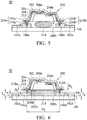
- FIG. 5 illustrates a cross-sectional view of the display device 40 in accordance with some embodiments of the present disclosure.
- the difference between the display device 40 in FIG. 5 and the display device 30 in FIG. 4 is that the first connecting post 210a and the second connecting post 210b include multilayer structures in the embodiment shown in FIG. 5 .
- the first connecting post 210a includes a first layer 210a' and a second layer 210a
- the second connecting post 210b includes a first layer 210b' and a second layer 210b".
- the first layer 210a' of the first connecting post 210a and the first layer 210b' of the second connecting post 210b may be formed of the same material as that of the conductive layer 208 in accordance with some embodiments.
- the first layer 210a' and the first layer 210b' may be formed of a conductive material having a relatively high melting temperature.
- the second layer 210a" of the first connecting post 210a and the second layer 210b" of the second connecting post 210b may be formed of a conductive material having a relatively low melting temperature compared to the material of the first layer 210a' and the first layer 210b' respectively.
- the second layer 210a" and the second layer 210b" is formed of a conductive material having a relatively high melting temperature compared to the material of the first pad 104a and the second pad 104b respectively.
- FIG. 6 illustrates a cross-sectional view of the display device 50 in accordance with some embodiments of the present disclosure.
- the adhesive layer 214 is filled in the space between the electronic device 200 and the first substrate 100 in the embodiment shown in FIG. 6 .
- the adhesive layer 214 is substantially filled in the space defined by the semiconductor die 202, the first dielectric layer 206, the first connecting post 210a, the second connecting post 210b, the first pad 104a, the second pad 104b respectively and the first substrate 100.
- the adhesive layer 214 is in physical contact with the first pad 104a and the second pad 104b.
- the adhesive layer 214 is also in physical contact with the first connecting post 210a and the second connecting post 210b.
- FIG. 7 illustrates a cross-sectional view of the display device 60 in accordance with some embodiments of the present disclosure.
- the difference between the display device 60 in FIG. 7 and the display device 50 in FIG. 6 is that the adhesive layer 214 further extends over the first pad 104a and the second pad 104b respectively located outside the first connecting post 210a and the second connecting post 210b in the embodiment shown in FIG. 7 .
- the adhesive layer 214 substantially covers the entire first pad 104a and second pad 104b.
- the edge of the adhesive layer 214 may be substantially aligned with the edge of the first pad 104a and/or the second pad 104b.
- FIGs. 8A-8E illustrate the cross-sectional views of the region M in FIG. 1 in accordance with some embodiments. It should be understood that some of the elements are omitted for clarity. In addition, it should be understood that only the second metal line 102b and the second pad 104b are shown in FIGs. 8A-8E for illustration, the first metal line 102a and the first pad 104a (not illustrated) may have the same or similar features. As described above, at least a portion of the first connecting post 210a and the second connecting post 210b are respectively embedded in the first pad 104a and the second pad 104b.
- the second pad 104b includes a bulging portion 104p around the portion of the second connecting post 210b that is embedded in the second pad 104b in accordance with some embodiments.
- the bulging portion 104p surrounds a portion of the second connecting post 210b that is buried in the second pad 104b.
- FIG. 8B in some embodiments where the adhesive layer 214 is filled in the space between the electronic device 200 and the first substrate 100 (as shown in FIG.
- the pad includes a bulging portion 104p
- the adhesive layer 214 also includes a swelling portion 214p around the portion of the connecting post that is embedded in the pad.
- FIG. 8C in some embodiments where the adhesive layer 214 is filled in the space between the electronic device 200 and the first substrate 100 (as shown in FIG. 6 ), the adhesive layer 214 includes a swelling portion 214p around the second connecting post 210b while the second pad 104b does not extrude.
- FIG. 8D in some other embodiments where the adhesive layer 214 substantially covers the entire second pad 104b (as shown in FIG.
- the second pad 104b includes a bulging portion 104p
- the adhesive layer 214 also includes a swelling portion 214p around the portion of the second connecting post 210b that is embedded in the second pad 104b.
- the adhesive layer 214 in some other embodiments where the adhesive layer 214 substantially covers the entire second pad 104b (as shown in FIG. 7 ), the adhesive layer 214 includes a swelling portion 214p around the second connecting post 210b while the second pad 104b is not extruded.
- the bulging portion 104p of the second pad 104b has a height H 3 (as shown in FIG. 8A ).
- the height H 3 may be defined as the distance between the highest point of the bulging portion 104p and the lowest point of the bulging portion 104p in the X direction of first substrate 100.
- the height H 3 of the bulging portion 104p may be in a range from about 0.1 ⁇ m to about 5 ⁇ m, or from about 1 um to about 3 um.
- the bulging portion 104p and the swelling portion 214p have a total height H 3 ' (as shown in FIG.
- the total height H 3 ' may be defined as the distance between the highest point of the swelling portion 214p and the lowest point of the bulging portion 104p in the X direction of first substrate 100.
- the height H 3 ' of the bulging portion 104p and the swelling portion 214p may be in a range from about 0.1 ⁇ m to about 5 ⁇ m, or from about 1 um to about 3 um.
- the adhesive layer 214 includes the swelling portion 214p
- the swelling portion 214p of the adhesive layer 214 has a height H 3 " (as shown in FIG. 8E ).
- the height H 3 " may be defined as the distance between the highest point of the swelling portion 214p and the lowest point of the swelling portion 214p in the normal direction (X direction) of first substrate 100. In some embodiments, the height H 3 " of the swelling portion 214p may be in a range from about 0.1 ⁇ m to about 5 ⁇ m, or from about 1 um to about 3 um.
- the portion of the second connecting post 210b that is embedded in the second pad 104b has a height H 4 (as shown in FIG. 8A ). In some embodiments, the portion of the second connecting post 210b that is embedded in the second pad 104b and the adhesive layer 214 has a height H 4 (as shown in FIG. 8D ). In some embodiments, the portion of the second connecting post 210b that is embedded in the adhesive layer 214 has a height H 4 (as shown in FIG. 8E ). As described above, the first connecting post 210a and the second connecting post 210b may respectively have a height H 1 and a height H 2 in the normal direction (X direction) of the first substrate 100.
- the ratio of the height H 4 of the portion of the second connecting post 210b that is embedded in the second pad 104b and/or the adhesive layer 214 to the height H 2 of the second connecting post 210b is in a range from 0.1 to 1 (i.e. 0.1 ⁇ H 4 /H 2 ⁇ 1).
- the portion of the first connecting post 210a that is embedded in the first pad 104a and the adhesive layer 214 has a height H 5 (not illustrtaed).
- the ratio of the height H 5 of the portion of the first connecting post 210a that is embedded in the first pad 104a and/or the adhesive layer 214 to the height H 1 of the first connecting post 210a is in a range from 0.1 to 1 (i.e. 0.1 ⁇ H 5 /H 1 ⁇ 1).
- FIG. 9 illustrates a cross-sectional view of the display device 70 in accordance with some embodiments of the present disclosure.
- the electronic device 200 is arranged in flip chip type in the embodiment shown in FIG.9 .
- the conductive layer 208 may directly serve as the connecting posts to embed in the first pad 104a and the second pad 104b.
- the electronic device 200 may be electrically connected to the first pad 104a and the second pad 104b by the portion of the conductive layer 208 that is embedded in the pad.
- FIG. 10 illustrates a cross-sectional view of the display device 80 in accordance with some embodiments of the present disclosure.
- the display device 80 includes an integrated electronic component 200A and a second substrate 300 disposed below the integrated electronic component 200A.
- the integrated electronic component 200A is substantially the same as the display device 10 described in FIG. 1 .
- the integrated electronic component 200A includes the first substrate 100, the first metal line 102a and the second metal line 102b disposed on the first substrate 100, and the first pad 104a and the second pad 104b disposed on the first substrate 100.
- the first pad 104a and the second pad 104b are electrically connected to the first metal line 102a and the second metal line 102b respectively.
- the integrated electronic component 200A also includes the electronic device 200 disposed on the first pad 104a and the second pad 104b.
- the electronic device 200 includes the first connecting post 210a and the second connecting post 210b, and a portion of the first connecting post 210a is embedded in the first pad 104a and a portion of the second connecting post 210b is embedded in the second pad 104b.
- the materials, manufacturing methods and functions of these elements are the same or similar to those described above, and thus are not repeated herein.
- the second substrate 300 may serve as a destination substrate (such as an array substrate) of the display device 80.
- the first substrate 100 serves as an intermediate substrate to carry the elements formed thereon to the destination substrate (e.g., the second substrate 300).
- a plurality of electronic devices 200 are disposed on the first substrate 100.
- the electronic device 200 may include, but is not limited to, a digital circuit, an LED, a photodiode, a transistor, or any other suitable electronic devices.
- the electronic device 200 may be a micro LED in accordance with some embodiments.
- the electronic device 200 further includes at least one integrated circuit 400 disposed on the first substrate 100.
- the electronic device 200 includes a circuit having multiple integrated circuits, other electronic elements or other optoelectronic elements and conductive wires interconnecting the multiple electronic elements to form a circuit on the first substrate 100.
- the first substrate 100 may carry the integrated electronic component 200A where multiple elements are formed and disposed on the second substrate 300, and thus may reduce the times that are required for the transfer.
- the material of the second substrate 300 may include, but is not limited to, glass, quartz, sapphire, polycarbonate (PC), polyimide (PI), polyethylene terephthalate (PET), rubbers, glass fibers, other polymer materials, any other suitable substrate material, or a combination thereof.
- the second substrate 300 may be formed of a metal-glass fiber composite plate, a metal-ceramic composite plate, a printed circuit board, or any other suitable material, but it is not limited thereto.
- the material of the second substrate 300 may be the same as or different than the material of the first substrate 100.
- the display device 80 also includes a third metal line 302a and a fourth metal line 302b disposed on the second substrate 300.
- the third metal line 302a and the fourth metal line 302b may be any conductive material on the second substrate 300.
- the third metal line 302a and the fourth metal line 302b each may be the conductive materials s of the circuit on the array substrate.
- the third metal line 302a and the fourth metal line 302b may be the data line or scan line on the array substrate.
- the third metal line 302a and the fourth metal line 302b may respectively have a thickness T 5 and a thickness T 6 in the normal direction (X direction) of the first substrate 100.
- the thickness T 5 of the third metal line 302a may be in a range from about 0.1um to about 1um, or from about 0.2um to about 0.6um. In some embodiments, the thickness T 6 of the fourth metal line 302b may be in a range from about 0.1um to about 1um, or from about 0.2um to about 0.6um. The thickness T 5 of the third metal line 302a may be the same with or different from the thickness T 6 of the fourth metal line 302b.
- the third metal line 302a and the fourth metal line 302b each may be formed of conductive materials.
- the conductive material for forming the third metal line 302a and the fourth metal line 302b may include, but is not limited to, copper, aluminum, tungsten, titanium, gold, silver, molybdenum, copper alloys, aluminum alloys, tungsten alloys, titanium alloys, gold alloys, silver alloys, molybdenum alloys, any other suitable conductive materials, or a combination thereof.
- the third metal line 302a and the fourth metal line 302b each may be formed of a conductive material having a relatively high melting temperature.
- the third metal line 302a and the fourth metal line 302b each may be formed of a conductive material having a melting temperature in a range from about 660°C to about 3410 °C.
- the third metal line 302a and/or the fourth metal line 302b may include multilayer structures.
- the display device 80 also includes a third pad 304a and a fourth pad 304b disposed on the second substrate 300.
- the third pad 304a and the fourth pad 304b are electrically connected to the third metal line 302a and the fourth metal line 302b respectively.
- the third pad 304a provides the electrical connection between the integrated electronic component 200A and the third metal line 302a on the second substrate 300.
- the fourth metal line 302b provides the electrical connection between the integrated electronic component 200A and the fourth metal line 302b on the second substrate 300. As shown in FIG.
- the third pad 304a and the fourth pad 304b at least partially overlaps the third metal line 302a and the fourth metal line 302b respectively, so that the electrical connection between the third pad 304a and the third metal line 302a, and between the fourth pad 304b and the fourth metal line 302b may be well maintained.
- the overlap between the pads and the metal lines may assist in the transmission of the electrical signals in the metal lines or reduce the possibility of leakage of electricity.
- the third pad 304a and the fourth pad 304b may respectively have a thickness T 7 and a thickness T 8 in the normal direction (X direction) of the first substrate 100.
- the thickness T 7 of the third pad 304a may be in a range from about 0.2um to about 50um, or from about 5um to about 15um.
- the thickness T 8 of the fourth pad 304b may be in a range from about 0.2um to about 50um, or from about 5um to about 15um.
- the thickness T 7 of the third pad 304a may be the same as or different than the thickness T 8 of the fourth pad 304b.
- the thickness T 7 of the third pad 304a is greater than the thickness T 5 of the third metal line 302a. In some embodiments, the thickness T 8 of the fourth pad 304b is greater than the thickness T 6 of the fourth metal line 302b. Furthermore, since the third pad 304a needs to transfer more current compared to the first pad 104a, an area (or a size) of the third pad 304a is greater than an area (or a size) of the first pad 104a in accordance with some embodiments.
- an area (or a size) of the fourth pad 304b is greater than an area (or a size) of the second pad 104b in accordance with some embodiments.
- the third pad 304a and the fourth pad 304b each may be formed of the same or different conductive materials.
- the conductive material for forming the third pad 304a and the fourth pad 304b may include, but is not limited to, solder materials, tin, indium, gallium, tin alloys, indium alloys, gallium alloys, gallium-indium alloys or a combination thereof.
- the third pad 304a and the fourth pad 304b each may be formed of conductive materials having a relatively low melting temperature.
- the third pad 304a and the fourth pad 304b each may be formed of a conductive material having a relatively low melting temperature compared to the melting temperature of the third metal line 302a and the fourth metal line 302b respectively.
- the third pad 304a and the fourth pad 304b each may be formed of conductive materials having a temperature in a range from about 100°C to about 400°C.
- the first metal line 102a of the integrated electronic component 200A further includes a third connecting post 310a and the second metal line 102b of the integrated electronic component 200A further includes a fourth connecting post 310b.
- the third connecting post 310a and the fourth connecting post 310b are electrically connected to the first metal line 102a and the second metal line 102b respectively.
- the first metal line 102a and the second metal line 102b extend from the first substrate 100 toward the second substrate 300 to provide the electrical connection between the integrated electronic component 200A and the second substrate 300.
- the third connecting post 310a and the fourth connecting post 310b extend toward the first substrate 100.
- the third connecting post 310a and the fourth connecting post 310b extend toward the third pad 304a and the fourth pad 304b respectively.
- the third connecting post 310a and the fourth connecting post 310b are in contact with the third pad 304a and the fourth pad 304b respectively.
- at least a portion of the third connecting post 310a is embedded in the third pad 304a and at least a portion of the fourth connecting post 310b is embedded in the fourth pad 304b.
- the third connecting post 310a is electrically connected to the third pad 304a and the fourth connecting post 310b is electrically connected to the fourth pad 104d.
- the connecting posts (the third connecting post 310a and the fourth connecting post 310b) and the metal lines (the first metal line 102a and the second metal line 102b) are integrally formed.
- the connecting posts and the metal lines may be a continuous structure. In some other embodiments, the connecting posts and the metal lines are separately formed.
- the connecting posts and the metal lines may be independent elements.
- the connecting posts (the third connecting post 310a and the fourth connecting post 310b) and the metal lines (the first metal line 102a and the second metal line 102b) may be formed of the same or different materials.
- the third connecting post 310a and the fourth connecting post 310b may be formed of the same or different materials.
- the third connecting post 310a and the fourth connecting post 310b may be formed of the same or different conductive materials.
- the conductive material for forming the third connecting post 310a and the fourth connecting post 310b may include, but is not limited to, copper, aluminum, tungsten, titanium, gold, silver, molybdenum, copper alloys, aluminum alloys, tungsten alloys, titanium alloys, gold alloys, silver alloys, molybdenum alloys, any other suitable conductive materials, or a combination thereof.
- the third connecting post 310a and the fourth connecting post 310b each may be formed of a conductive material having a relatively high melting temperature.
- the third connecting post 310a and the fourth connecting post 310b each may be formed of a conductive material having a melting temperature in a range from about 660°C to about 3410°C.
- the third connecting post 310a and the fourth connecting post 310b each may be formed of a conductive material having a relatively high melting temperature compared to the material of the third pad 304a and the fourth pad 304b.
- the first metal line 102a and the second metal line 102b each may be formed of a conductive material having a relatively high melting temperature compared to the material of the third pad 304a and the fourth pad 304b.
- the first connecting post 210a and the second connecting post 210b are separated apart from each other by a distance D 1 .
- the distance D 1 between the first connecting post 210a and the second connecting post 210b is in a range from about 1 um to about 200 um, or from about 2um to about 50um.
- the third connecting post 310a and the fourth connecting post 310b are separated apart from each other by a distance D 2 .
- the distance D 2 between the third connecting post 310a and the fourth connecting post 310b is in a range from about 3um to about 600um, or from about 6um to about 150um.
- the distance D 2 between the third connecting post 310a and the fourth connecting post 310b is greater than the distance D 1 between the first connecting post 210a and the second connecting post 210b.
- the width D4 in Y direction of the third connecting post 310a may be greater than the width D3 in Y direction of the first connecting post 210a.
- the width or size of the fourth connecting post 310b may be greater than the width or size of the second connecting post 210b.
- the melting temperature of the third connecting post 310a and the fourth connecting post 310b is higher than the melting temperature of the third pad 304a and the fourth pad 304b respectively in accordance with some embodiments.
- the melting temperature of the metal lines (the first metal line 102a, the second metal line 102b, the third metal line 302a and the fourth metal line 302b) is higher than the melting temperature of the pads (the first pad 104a and the second pad 104b).
- the ratio of the melting temperature of the metal lines to the melting temperature of the pads is in a range from about 1.5 to about 35, or from about 1.5 to about 17 in accordance with some embodiments.
- the ratio of the melting temperature of the metal lines to the melting temperature of the pads should not be too small, or the metal lines may also be melted or deformed during the heating process and may cause the risk of broken metal lines.
- the ratio of the melting temperature of the metal lines to the melting temperature of the pads should not be too great, or the difference between the coefficient of expansion of the metal lines and the coefficient of expansion of the pads may be too great so that the metal lines and the pads may be peeled off.
- the third pad 304a and the fourth pad 304b may be formed of a conductive material having a relatively low melting temperature compared to the material of the metal lines.
- the conductive material having a relatively low melting temperature for forming the pad may include, but is not limited to, solder materials, tin, indium, gallium, tin alloys, indium alloys, gallium alloys, or gallium-indium alloys.
- the third connecting post 310a and the fourth connecting post 310b may be formed of a conductive material having a relatively high melting temperature compared to the material of the pads.
- the conductive material having a relatively high melting temperature for forming the connecting posts may include, but is not limited to, copper, aluminum, tungsten, titanium, gold, silver, molybdenum, copper alloys, aluminum alloys, tungsten alloys, titanium alloys, gold alloys, silver alloys, or molybdenum alloys.
- the third metal line 302a and the fourth metal line 302b may also be formed of a conductive material having a relatively high melting temperature compared to the material of the pads.
- the conductive material having a relatively high melting temperature for forming the third metal line 302a and the fourth metal line 302b may include, but is not limited to, copper, aluminum, tungsten, titanium, gold, silver, molybdenum, copper alloys, aluminum alloys, tungsten alloys, titanium alloys, gold alloys, silver alloys, or molybdenum alloys.
- the display device 80 also includes an adhesive layer 314 disposed between the first substrate 100 and the second substrate 300.
- the adhesive layer 314 adhere the first substrate 100 and the second substrate 300 together and the third connecting post 310a and the fourth connecting post 310b are held in physical contact with the third pad 304a and the fourth pad 304b on the second substrate 300 respectively.
- the adhesive layer 314 may be formed of adhesive materials.
- the adhesive layer 314 may be an insulator.
- the material of the adhesive layer 314 may include, but is not limited to, heat-curing adhesives, light-curing adhesives, or a combination thereof.
- the light-curing adhesives may include UV light-curing adhesives or visible light-curing adhesives.
- the material of the adhesive layer 314 may be the same as or different than the material of the adhesive layer 214.
- FIGs. 11A-11C illustrate the diagrams showing the transfer process of the electronic devices to the destination substrate in accordance with some embodiments of the present disclosure.
- the first substrate 100 may include multiple electronic devices 200 formed thereon. It should be understood that although only the electronic devices 200 are illustrated in FIG. 11A , the first substrate 100 may actually include various elements formed thereon (as shown in the FIG. 10 ). In this embodiment, the first substrate 100 serves as an intermediate substrate to gather the various elements such as the electronic devices 200 first and then transfer these elements to the second substrate 300 (e.g. a destination substrate).
- the electronic devices 200 may be the micro LEDs emitting red light, green light, blue light, or a combination thereof.
- more than one intermediate substrate may be transferred to the second substrate 300 and the intermediate substrates may carry different electronic devices.
- the first substrate 100, 100' and 100" may carry the different electronic devices 200, 200' and 200" respectively, and the electronic devices 200, 200' and 200" may be integrated on the second substrate 300 first.
- the second substrate 300 encompassing the integrated electronic component then may be transferred to another destination substrate.
- the electronic devices 200, 200' and 200" may be the micro LEDs emitting red light, green light and blue light respectively.
- the small electronic devices may be integrated on the intermediate substrate first and then the intermediate substrate carrying the integrated small electronic devices can be transferred to a destination substrate (e.g. an array substrate of the display device). Therefore, compared with transferring the small electronic devices one by one, the times that are required for transfer the small electronic device by an intermediate substrate are greatly reduced.
- the present disclosure provides a structure for improving the efficiency of the electrical connection between relatively small electronic devices such as mini LEDs, micro LEDs, orgnic LEDs, inorgnic LEDs (e.g. quautum-dot LEDs) or integrated electronic components and a relatively large destination substrate such as an array substrate.
- the display device provided in the present disclosure includes the connecting posts that can be securely embedded in the conductive elements of the destination substrate, such as the pads for the interconnection.
- the electronic devices can therefore maintain effective electrical connection to the circuit system on the destination substrate.
- the configuration of the intermediate substrate in the display device may reduce the times that are required for the transfer of the small electronic devices to the destination substrate in accordance with some embodiments of the present disclosure.
Landscapes
- Engineering & Computer Science (AREA)
- Mechanical Engineering (AREA)
- Microelectronics & Electronic Packaging (AREA)
- Devices For Indicating Variable Information By Combining Individual Elements (AREA)
- Physics & Mathematics (AREA)
- Geometry (AREA)
- Manufacturing & Machinery (AREA)
Abstract
Description
- The present disclosure relates to a display device, and in particular it relates to the interconnection of the electronic components in the display device.
- Electronic products that come with a display panel, such as smartphones, tablets, notebooks, monitors, and TVs, have become indispensable necessities in modern society. With the flourishing development of such portable electronic products, consumers have high expectations regarding the quality, the functionality, and the price of such products. The development of next-generation display devices has been focused on techniques that are energy-saving and environmentally friendly.
- Micro LED technology is an emerging flat panel display technology. Micro LED displays drive an array of addressed micro LEDs. Micro LED displays may produce seamless images with a wide viewing angle, high brightness, and high contrast. However, due to the small size of a micro LED, integration and packaging issues are one of the main obstacles for commercialization of such products.
- Using current manufacturing methods, micro LEDs are generally formed and divided into several micro LED dies (e.g., micro-lighting dies) on a wafer substrate and then transferred to another destination substrate. For example, the driving circuits and related circuits are formed on the destination substrate to provide an array substrate (e.g., a TFT array substrate), and the micro LED dies are then mounted on the array substrate. Due to the small size of micro LED dies, transferring the micro LED dies to the destination substrate is a burdensome task. In addition, the electrical connections between the micro LED (including the integrated electronic component where these dies are formed) and the destination substrate is also a problem that needs to be taken care of.
- Accordingly, it is the problem the invention wants to solve is to develop a structure and method that can effectively maintain or improve the efficiency of the transfer, or improve the electrical interconnection of a small electronic component such as a micro LED to a destination substrate.
- This problem is inventively solved by a display device according to
claim 1. The display device includes a substrate and a first metal line and a second metal line disposed on the substrate. The display device also includes a first pad and a second pad disposed on the substrate and electrically connected to the first metal line and the second metal line respectively. The display device further includes an electronic device disposed on the first pad and the second pad. The electronic device includes a first connecting post and a second connecting post, wherein a distance between the first connecting post and the second connecting post is in a range from 1um to 200um. A portion of the first connecting post is embedded in the first pad and a portion of the second connecting post is embedded in the second pad. - Furthermore, the problem is solved by a display device according to claim 11. The display device includes an integrated electronic component, a second substrate disposed below the integrated electronic component, and a third pad and a fourth pad disposed on the second substrate and electrically connected to the first metal line and the second metal line respectively. The integrated electronic component includes a first substrate and a first metal line and a second metal line disposed on the first substrate. The integrated electronic component also includes a first pad and a second pad disposed on the first substrate and electrically connected to the first metal line and the second metal line respectively. The integrated electronic component further includes an electronic device disposed on the first pad and the second pad, and the electronic device includes a first connecting post and a second connecting post. A portion of the first connecting post is embedded in the first pad and a portion of the second connecting post is embedded in the second pad. The first metal line includes a third connecting post and the second metal line includes a fourth connecting post. The third connecting post and the fourth connecting post are electrically connected to the third pad and the fourth pad respectively.
- A detailed description is given in the following embodiments with reference to the accompanying drawings.
- The disclosure may be more fully understood by reading the subsequent detailed description and examples with references made to the accompanying drawings, wherein:
-
FIG. 1 illustrates the cross-sectional views of the display device in accordance with some embodiments of the present disclosure. -
FIGs. 2A-2D illustrate the cross-sectional views of the metal lines and the pads in the region M inFIG. 1 in accordance with some embodiments. -
FIG. 2E and FIG. 2F illustrate the top views of the metal lines and the pads in the region M inFIG. 1 in accordance with some embodiments. -
FIGs. 3-7 illustrate the cross-sectional views of the display device in accordance with some embodiments of the present disclosure. -
FIGs. 8A-8E illustrate the cross-sectional views of the region M inFIG. 1 in accordance with some embodiments. -
FIG. 9 illustrate a cross-sectional view of the display device in accordance with some embodiments of the present disclosure. -
FIG. 10 illustrates a cross-sectional view of the display device in accordance with some embodiments of the present disclosure. -
FIGs. 11A-11C illustrate the diagrams showing the transfer process of the electronic devices to the destination substrate in accordance with some embodiments of the present disclosure. - The display device of the present disclosure and the manufacturing method thereof are described in detail in the following description. In the following detailed description, for purposes of explanation, numerous specific details and embodiments are set forth in order to provide a thorough understanding of the present disclosure. The specific elements and configurations described in the following detailed description are set forth in order to clearly describe the present disclosure. It will be apparent, however, that the exemplary embodiments set forth herein are used merely for the purpose of illustration, and the inventive concept may be embodied in various forms without being limited to those exemplary embodiments. In addition, the drawings of different embodiments may use like and/or corresponding numerals to denote like and/or corresponding elements in order to clearly describe the present disclosure. However, the use of like and/or corresponding numerals in the drawings of different embodiments does not suggest any correlation between different embodiments. In addition, in this specification, expressions such as "first material layer disposed on/over a second material layer", may indicate the direct contact of the first material layer and the second material layer, or it may indicate a non-contact state with one or more intermediate layers between the first material layer and the second material layer. In the above situation, the first material layer may not be in direct contact with the second material layer.
- It should be noted that the elements or devices in the drawings of the present disclosure may be present in any form or configuration known to those with ordinary skill in the art. In addition, the expressions "a layer overlying another layer", "a layer is disposed above another layer", "a layer is disposed on another layer" and "a layer is disposed over another layer" may indicate that the layer is in direct contact with the other layer, or that the layer is not in direct contact with the other layer, there being one or more intermediate layers disposed between the layer and the other layer.
- In addition, in this specification, relative expressions are used. For example, "lower", "bottom", "higher" or "top" are used to describe the position of one element relative to another. It should be appreciated that if a device is flipped upside down, an element that is "lower" will become an element that is "higher".
- It should be understood that, although the terms first, second, third etc. may be used herein to describe various elements, components, regions, layers, portions and/or sections, these elements, components, regions, layers, portions and/or sections should not be limited by these terms. These terms are only used to distinguish one element, component, region, layer, portion or section from another element, component, region, layer or section. Thus, a first element, component, region, layer, portion or section discussed below could be termed a second element, component, region, layer, portion or section without departing from the teachings of the present disclosure.
- It should be understood that this description of the exemplary embodiments is intended to be read in connection with the accompanying drawings, which are to be considered part of the entire written description. The drawings are not drawn to scale. In addition, structures and devices are shown schematically in order to simplify the drawing.
- The terms "about" and "substantially" typically mean +/- 20% of the stated value, more typically +/- 10% of the stated value, more typically +/- 5% of the stated value, more typically +/- 3% of the stated value, more typically +/- 2% of the stated value, more typically +/- 1% of the stated value and even more typically +/- 0.5% of the stated value. The stated value of the present disclosure is an approximate value. When there is no specific description, the stated value includes the meaning of "about" or "substantially".
- Unless defined otherwise, all technical and scientific terms used herein have the same meaning as commonly understood by one of ordinary skill in the art to which this disclosure belongs. It should be appreciated that, in each case, the term, which is defined in a commonly used dictionary, should be interpreted as having a meaning that conforms to the relative skills of the present disclosure and the background or the context of the present disclosure, and should not be interpreted in an idealized or overly formal manner unless so defined.
- In addition, in some embodiments of the present disclosure, terms concerning attachments, coupling and the like, such as "connected" and "interconnected," refer to a relationship wherein structures are secured or attached to one another either directly or indirectly through intervening structures, as well as both movable or rigid attachments or relationships, unless expressly described otherwise.
- The present disclosure provides a structure for improving the efficiency of the electrical connection between relatively small electronic devices such as mini LEDs, micro LEDs, orgnic LEDs, inorgnic LEDs (e.g. quautum-dot LEDs) or integrated electronic components and a relatively large destination substrate such as an array substrate. The display device provided in the present disclosure includes the connecting posts that can be securely embedded in the conductive elements of the destination substrate, such as the pads for the interconnection. The electronic devices can therefore maintain effective electrical connection to the circuit system on the destination substrate. In addition, the configuration of the intermediate substrate in the display device may reduce the times that are required for the transfer of the small electronic devices to the destination substrate in accordance with some embodiments of the present disclosure.
-
FIG. 1 illustrates a cross-sectional view of thedisplay device 10 in accordance with some embodiments of the present disclosure. It should be understood that additional features may be added to the display device in accordance with some embodiments of the present disclosure. Some of the features described below may be replaced or eliminated in accordance with some embodiments of the present disclosure. - Referring to
FIG. 1 , thedisplay device 10 includes afirst substrate 100 and anelectronic device 200 disposed on thefirst substrate 100. Thefirst substrate 100 may be an intermediate substrate or a destination substrate (such as an array substrate) of thedisplay device 10. In some embodiments, the material of thefirst substrate 100 may include, but is not limited to, glass, quartz, sapphire, polycarbonate (PC), polyimide (PI), polyethylene terephthalate (PET), rubbers, glass fibers, other polymer materials, any other suitable substrate material, or a combination thereof. In some embodiments, thefirst substrate 100 may be formed of a metal-glass fiber composite plate, a metal-ceramic composite plate, a printed circuit board, or any other suitable material, but it is not limited thereto. - The
display substrate 10 also includes afirst metal line 102a and asecond metal line 102b disposed on thefirst substrate 100. Thefirst metal line 102a and thesecond metal line 102b may be any conductive element on thefirst substrate 100. For example, thefirst metal line 102a and thesecond metal line 102b each may be the conductive elements of the circuit on the array substrate. In some embodiments, thefirst metal line 102a and thesecond metal line 102b may be the data line or scan line on the array substrate. Thefirst metal line 102a and thesecond metal line 102b may respectively have a thickness T1 and a thickness T2 in the X direction of thefirst substrate 100, for example, in the X direction as shown inFIG. 1 , and X direction is the normal direction of thefirst substrate 100. In some embodiments, the thickness T1 of thefirst metal line 102a may be in a range from about 0.1µm to about 1µm, or from about 0.2um to about 0.6um. In some embodiments, the thickness T2 of thesecond metal line 102b may be in a range from about 0.1µm to about 1µm, or from about 0.2 um to about 0.6um. The thickness T1 of thefirst metal line 102a may be the same as or different than the thickness T2 of thesecond metal line 102b. - In some embodiments, the
first metal line 102a and thesecond metal line 102b may be formed of the same or different conductive materials. The conductive material for forming thefirst metal line 102a and thesecond metal line 102b may include, but is not limited to, copper, aluminum, tungsten, titanium, gold, silver, molybdenum, copper alloys, aluminum alloys, tungsten alloys, titanium alloys, gold alloys, silver alloys, molybdenum alloys, any other suitable conductive materials, or a combination thereof. In some embodiments, thefirst metal line 102a and thesecond metal line 102b each may be formed of a conductive material having a relatively high melting temperature. In some embodiments, thefirst metal line 102a and thesecond metal line 102b each may be formed of a conductive material having a melting temperature in a range from about 660°C to about 3410 °C. - In addition, in some embodiments, the
first metal line 102a and/or thesecond metal line 102b may include multilayer structures. For example,FIG. 2A illustrates a cross-sectional view of the metal lines (thefirst metal line 102a and thesecond metal line 102b) and the pads (thefirst pad 104a and thesecond pad 104b) in the region M inFIG. 1 in accordance with some embodiments. As shown inFIG. 2A , themetal line 102a/102b may include at least two layers in accordance with some embodiments. In particular, themetal line 102a/102b may be a coaxial two-layer structure, which includes aninner layer 102g and anouter layer 102f. In certain embodiments, theinner layer 102g is made of aluminum and theouter layer 102f is made of molybdenum. In addition, it should be understood that only thesecond metal line 102b and thesecond pad 104b are shown inFIGs. 2A-2F for illustration, thefirst metal line 102a and thefirst pad 104a (not illustrated) may have the same or similar features. - Next, referring back to
FIG. 1 , thedisplay substrate 10 also includes afirst pad 104a and asecond pad 104b disposed on thefirst substrate 100. Thefirst pad 104a and thesecond pad 104b are electrically connected to thefirst metal line 102a and thesecond metal line 102b respectively. In other words, thefirst pad 104a provides the electrical connection between theelectronic device 200 and thefirst metal line 102a on thefirst substrate 100. Thesecond pad 104b provides the electrical connection between theelectronic device 200 and thesecond metal line 102b on thefirst substrate 100. As shown inFIG. 1 , thefirst pad 104a and thesecond pad 104b at least partially overlaps thefirst metal line 102a and thesecond metal line 102b respectively, so that the electrical connection between thefirst pad 104a and thefirst metal line 102a, and between thesecond pad 104b and the second metal line 102bmay be well maintained. In particular, the overlap between thefirst pad 104a and thefirst metal line 102a, and between thesecond pad 104b and thesecond metal line 102b may respectively assist in the transmission of the electrical signals in thefirst metal line 102a and thesecond metal line 102b or reduce the possibility of leakage of electricity. - The configurations of the
second metal line 102b and the second pad 104bin accordance with some embodiments of the present disclosure are described in detail inFIGs. 2B-2D. FIGs. 2B-2D illustrate the cross-sectional views of thesecond metal line 102b and thesecond pad 104b in the region M inFIG. 1 in accordance with some embodiments. It should be understood that the elements other than the metal line and the pad are omitted for clarity. - As shown in
FIG. 2B , a portion of thesecond pad 104b overlaps thesecond metal line 102b in accordance with some embodiments. Specifically, thesecond pad 104b may cover the sidewall and a portion of the top surface of thesecond metal line 102b. As shown inFIG. 2C and FIG. 2D , the entiresecond pad 104b is disposed on thesecond metal line 102b in accordance with some embodiments. Thesidewall 104s of thesecond pad 104b may be aligned with the sidewall 102s of thesecond metal line 102b in accordance with some embodiments (as shown inFIG. 2C ). Thesecond metal line 102b may further extend toward the center of theelectronic device 200 and the sidewall 102s of thesecond metal line 102b may protrude from thesidewall 104s of thesecond pad 104b in accordance with some embodiments (as shown inFIG. 2D ). - On the other hand,
FIG. 2E and FIG. 2F illustrate the top views of thesecond metal line 102b and thesecond pad 104b in the region M inFIG. 1 in accordance with some embodiments. In addition, the cross-sectional view along the line B-B' inFIG. 2E may correspond to the cross-sectional views as shown inFIG. 2B and FIG. 2C . The cross-sectional view along the line B-B' inFIG. 2F may correspond to the cross-sectional view as shown inFIG. 2D . Referring toFIGs. 2B, 2C and2E , thesecond pad 104b may entirely overlap aterminal portion 102e of thesecond metal line 102b in accordance with some embodiments. Referring toFIG. 2D andFIG. 2F , thesecond pad 104b may partially overlap theterminal portion 102e of thesecond metal line 102b in accordance with some other embodiments. In accordance with some embodiments of the present disclosure, the "terminal portion" may refer to the terminal portion of thesecond metal line 102b that extends from the sidewall 102s of thesecond metal line 102b inwardly for a range about 100 µm along the Y direction. - Next, referring back to
FIG. 1 , thefirst pad 104a and thesecond pad 104b may respectively have a thickness T3 and a thickness T4 in the X direction (i.e. the normal direction) of thefirst substrate 100. In some embodiments, the thickness T3 of thefirst pad 104a may be in a range from about 0.2µm to about 50µm, or from about 5um to about 15um. In some embodiments, the thickness T4 of thesecond pad 104b may be in a range from about 0.2µm to about 50µm, or from about 5um to about 15um. The thickness T3 of thefirst pad 104a may be the same as or different than the thickness T4 of thesecond pad 104b. In some embodiments, the thickness T3 of thefirst pad 104a is greater than the thickness T1 of thefirst metal line 102a. In some embodiments, the thickness T4 of thesecond pad 104b is greater than the thickness T2 of thesecond metal line 102b. - In some embodiments, the
first pad 104a and thesecond pad 104b each may be formed of conductive materials. The conductive material for forming thefirst pad 104a and thesecond pad 104b may include, but is not limited to, solder materials, tin, indium, gallium, tin alloys, indium alloys, gallium alloys, gallium-indium alloys or a combination thereof. In some embodiments, thefirst pad 104a and thesecond pad 104b each may be formed of conductive materials having a relatively low melting temperature. In particular, thefirst pad 104a and thesecond pad 104b each may be formed of a conductive material having a relatively low melting temperature compared to the melting temperature of thefirst metal line 102a and thesecond metal line 102b. In some embodiments, thefirst pad 104a and thesecond pad 104b each may be formed of conductive materials having a temperature in a range from about 100°C to about 400°C. - In some embodiments, the
first metal line 102a, thesecond metal line 102b, thefirst pad 104a and thesecond pad 104b may be formed by using chemical vapor deposition, physical vapor deposition, electroplating process, electroless plating process, any other suitable processes, or a combination thereof. The chemical vapor deposition may include, but is not limited to, low-pressure chemical vapor deposition (LPCVD), low-temperature chemical vapor deposition (LTCVD), rapid thermal chemical vapor deposition (RTCVD), plasma enhanced chemical vapor deposition (PECVD), or atomic layer deposition (ALD). The physical vapor deposition may include, but is not limited to, sputtering, evaporation, or pulsed laser deposition (PLD). - Still referring to
FIG. 1 , theelectronic device 200 includes asemiconductor die 202, afirst electrode 204a, asecond electrode 204b, a firstdielectric layer 206, aconductive layer 208, a first connectingpost 210a, a second connectingpost 210b, and asecond dielectric layer 212. Theelectronic device 200 may include an integrated circuit. For example, theelectronic device 200 may include, but is not limited to, a digital circuit, an LED, a photodiode, a transistor, or any other suitable electronic devices. Theelectronic device 200 may be a micro LED in accordance with some embodiments. It should be understood that although oneelectronic device 200 is illustrated inFIG. 1 , there may be more than oneelectronic device 200 disposed on thefirst substrate 100. - As shown in
FIG. 1 , theelectronic device 200 is disposed on thefirst pad 104a and thesecond pad 104b. The semiconductor die 202 of theelectronic device 200 may include multiple layers of different materials. In some embodiments, the semiconductor die 202 may include, but is not limited to, semiconductor layers, or quantum well layers. In some embodiments, the semiconductor layers may be formed of the III-V compounds. The III-V compounds may include, but is not limited to, gallium nitride (GaN), indium nitride (InN), aluminum nitride (AlN), indium gallium nitride (InGaN), aluminum gallium nitride (AlGaN), aluminum indium gallium nitride (AlGaInN) or a combination thereof. In some embodiments, the material of the quantum well layer may include, but is not limited to, indium gallium nitride, a gallium nitride or a combination thereof. - The semiconductor die 202 may be an organic micro LED die in accordance with some embodiments. The semiconductor die 202 may be an inorganic micro LED die in accordance with some embodiments. In some embodiments, the cross-sectional area of the semiconductor die 202 may have a length ranging from about 1µm to about 175µm in Y direction and may have a width ranging from about 1µm to about 175µm in Z direction. In some embodiments, the semiconductor die 202 may have a size ranging from about 1µm x 1µm x 1µm to about 175µm x 175µm x 175µm. In some embodiments, the semiconductor die 202 may be formed by using an epitaxial growth process. For example, metal organic chemical vapor deposition (MOCVD), molecular beam epitaxy (MBE), hydride vapor phase epitaxy (HVPE), liquid phase epitaxy (LPE), or another suitable process may be used to form the semiconductor die 202.
- The
first electrode 204a and thesecond electrode 204b may be disposed over the semiconductor die 202. In some embodiments where theelectronic device 200 is a micro LED, thefirst electrode 204a and thesecond electrode 204b may serve as the n-electrode and p-electrode of the micro LED respectively. In some embodiments, thefirst electrode 204a and thesecond electrode 204b may be formed of metallic conductive materials. The metallic conductive material may include, but is not limited to, copper, aluminum, tungsten, titanium, gold, silver, molybdenum, platinum, nickel, copper alloys, aluminum alloys, tungsten alloys, titanium alloys, gold alloys, silver alloys, molybdenum alloys, platinum alloys, nickel alloys, any other suitable conductive materials, or a combination thereof. In some embodiments, thefirst electrode 204a and thesecond electrode 204b may be formed of transparent conductive materials, for example, the transparent conductive material (TCO) may include, but is not limited to, indium tin oxide (ITO), tin oxide (SnO), zinc oxide (ZnO), indium zinc oxide (IZO), indium gallium zinc oxide (IGZO), indium tin oxide (ITZO), antimony tin oxide (ATO), antimony zinc oxide (AZO), or a combination thereof. It should be noted that, thefirst electrode 204a and thesecond electrode 204b may be formed of a material having a relatively high melting temperature compared with theconductive layer 208 ofelectronic device 200. In some embodiments, thefirst electrode 204a and thesecond electrode 204b may be formed by using chemical vapor deposition, physical vapor deposition, electroplating process, electroless plating process, any other suitable processes, or a combination thereof. - Still referring to
FIG. 1 , thefirst dielectric layer 206 is disposed over the semiconductor die 202. In some embodiments, thefirst dielectric layer 206 may cover a portion of thefirst electrode 204a and a portion of thesecond electrode 204b. In other words, thefirst dielectric layer 206 may partially expose thefirst electrode 204a and thesecond electrode 204b so that thefirst electrode 204a and thesecond electrode 204b may be electrically connected to theconductive layer 208. In some embodiments, thefirst dielectric layer 206 may include, but is not limited to, silicon oxide, silicon nitride, silicon oxynitride, high-k dielectric material, any other suitable dielectric material, or a combination thereof. The high-k dielectric material may include, but is not limited to, metal oxide, metal nitride, metal silicide, transition metal oxide, transition metal nitride, transition metal silicide, metal oxynitride, metal aluminate, zirconium silicate, zirconium aluminate. In some embodiments, thefirst dielectric layer 206 may be formed by using chemical vapor deposition, spin coating, any other suitable processes, or a combination thereof. - In addition, the
electronic device 200 includes theconductive layer 208 disposed over thefirst dielectric layer 206. As described above, theconductive layer 208 is in contact with portions of thefirst electrode 204a and thesecond electrode 204b. Theconductive layer 208 is electrically connected to thefirst electrode 204a and thesecond electrode 204b separately. In addition, as shown inFIG. 1 , theconductive layer 208 includes a first connectingpost 210a and a second connectingpost 210b. The first connectingpost 210a and the second connectingpost 210b are each defined as the portion that is substantially below thebottom side 200b of theelectronic device 200. The first connectingpost 210a and the second connectingpost 210b may protrude from thebottom surface 206b of thefirst dielectric layer 206 in accordance with some embodiments. The first connectingpost 210a and the second connectingpost 210b may also protrude from thebottom surface 202b of the semiconductor die 202 in accordance with some embodiments. In other words, the first connectingpost 210a and the second connectingpost 210b extend toward thefirst substrate 100. The first connectingpost 210a and the second connectingpost 210b extend toward thefirst pad 104a and thesecond pad 104b respectively. In addition, at least a portion of the first connectingpost 210a is embedded in thefirst pad 104a and at least a portion of the second connectingpost 210b is embedded in thesecond pad 104b. Thus, the first connectingpost 210a is electrically connected to thefirst pad 104a and the second connectingpost 210b is electrically connected to thesecond pad 104b. It should be understood that although two connecting posts are disposed in the embodiment shown inFIG. 1 , the amount of the connecting post may be adjusted according to the needs in some other embodiments. - As shown in
FIG. 1 , the first connectingpost 210a and the second connectingpost 210b are separated apart from each other by a distance D1. In some embodiments, the distance D1 between the first connectingpost 210a and the second connectingpost 210b is in a range from about 1 um to about 200 um, or from about 2um to about 50um. In some embodiments, the distance D1 between the first connectingpost 210a and the second connectingpost 210b is defined as the distance between any position within the first connectingpost 210a and any position within the second connectingpost 210b. In some other embodiments, the distance D1 between the first connectingpost 210a and the second connectingpost 210b is defined as the distance between the lowest point in the X direction of the first connectingpost 210a and the lowest point in the X direction of the second connectingpost 210b in a cross section. - Moreover, the first connecting
post 210a and the second connectingpost 210b may respectively have a height H1 and a height H2 in the X direction of thefirst substrate 100. In some embodiments, the height H1 of the first connectingpost 210a may be in a range from about 0.05µm to about 10µm, or from about 1um to about 5 um. In some embodiments, the height H2 of the second connectingpost 210b may be in a range from about 0.05µm to about 10µm, or from about 1 um to about 5 um. - In some embodiments, the first connecting
post 210a, the second connectingpost 210b and theconductive layer 208 are integrally formed. The first connectingpost 210a, the second connectingpost 210b and theconductive layer 208 may be a continuous structure. In some other embodiments, the first connectingpost 210a, the second connectingpost 210b and theconductive layer 208 are separately formed. The first connectingpost 210a, the second connectingpost 210b and theconductive layer 208 may be independent elements. In addition, the first connectingpost 210a and theconductive layer 208 may be formed of the same or different materials. Similarly, the second connectingpost 210b and theconductive layer 208 may be formed of the same or different materials. - In some embodiments, the first connecting
post 210a and the second connectingpost 210b each may be formed of conductive materials. The conductive material for forming the first connectingpost 210a and the second connectingpost 210b may include, but is not limited to, copper, aluminum, tungsten, titanium, gold, silver, molybdenum, copper alloys, aluminum alloys, tungsten alloys, titanium alloys, gold alloys, silver alloys, molybdenum alloys, any other suitable conductive materials, or a combination thereof. In some embodiments, the first connectingpost 210a and the second connectingpost 210b each may be formed of a conductive material having a relatively high melting temperature. In some embodiments, the first connectingpost 210a and the second connectingpost 210b each may be formed of a conductive material having a melting temperature in a range from about 660°C to about 3410°C. - The
second dielectric layer 212 is formed over theconductive layer 208. Thesecond dielectric layer 212 also covers the first connectingpost 210a and the second connectingpost 210b. In some embodiments, thesecond dielectric layer 212 may include, but is not limited to, silicon oxide, silicon nitride, silicon oxynitride, high-k dielectric material, any other suitable dielectric material, or a combination thereof. The high-k dielectric material may include, but is not limited to, metal oxide, metal nitride, metal silicide, transition metal oxide, transition metal nitride, transition metal silicide, metal oxynitride, metal aluminate, zirconium silicate, zirconium aluminate. In some embodiments, thesecond dielectric layer 212 may be formed by using chemical vapor deposition, spin coating, any other suitable processes, or a combination thereof. - In addition, the
display device 10 also includes anadhesive layer 214 disposed between theelectronic device 200 and thefirst substrate 100. Theadhesive layer 214 adhere theelectronic device 200 and thefirst substrate 100 together and the first connectingpost 210a and the second connectingpost 210b are held in physical contact with thefirst pad 104a and thesecond pad 104b on thefirst substrate 100 respectively. Theadhesive layer 214 may be formed of adhesive materials. In some embodiments, theadhesive layer 214 may be an insulator. In some embodiments, the material of theadhesive layer 214 may include, but is not limited to, heat-curing adhesives, light-curing adhesives, or a combination thereof. The light-curing adhesives may include UV light-curing adhesives or visible light-curing adhesives. - In some embodiments, the
adhesive layer 214 may be formed by using coating, spray coating, inkjet printing, any other suitable methods, or a combination thereof, but is not limited thereto. As shown inFIG.1 , theadhesive layer 214 may be formed in the shape of a drop in accordance with some embodiments. - It should be noted that, before the
electronic device 200 is affixed to thefirst substrate 100, thefirst substrate 100 and the elements formed thereon are heated in accordance with some embodiments. Specifically, thefirst pad 104a and thesecond pad 104b are heated to be in a melted state so that the first connectingpost 210a and the second connectingpost 210b can be embedded into thefirst pad 104a and thesecond pad 104b respectively. In some embodiments, the melting temperature of the connecting posts (the first connectingpost 210a and the second connectingpost 210b) is higher than the melting temperature of the pads (thefirst pad 104a and thesecond pad 104b). In such cases, the temperature of the heating process may be adjusted within a range where the pads are substantially melted and the connecting posts are not melted. In some other embodiments, the hardness of the connecting posts is higher than the hardness of the pads so that the connecting posts can be embedded into the pads. - In addition, since the
first metal line 102a and thesecond metal line 102b disposed on thefirst substrate 100 will also be heated during the heating process, the melting temperature of thefirst metal line 102a and thesecond metal line 102b is respectively higher than the melting temperature of thefirst pad 104a and thesecond pad 104b in accordance with some embodiments. Specifically, the ratio of the melting temperature of the metal lines to the melting temperature of the pads is in a range from about 1.5 to about 35, or from about 1.5 to about 17 in accordance with some embodiments. It should be noted that the ratio of the melting temperature of the metal lines to the melting temperature of the pads should not be too small, or the metal lines may also be melted or deformed during the heating process and may cause the risk of broken metal lines. The ratio of the melting temperature of the metal lines to the melting temperature of the pads should not be too great, or the difference between the coefficient of expansion of the metal lines and the coefficient of expansion of the pads may be too great so that the metal lines and the pads may be peeled off. - As described above, the
first pad 104a and thesecond pad 104b may be formed of a conductive material having a relatively low melting temperature compared to the material of thefirst metal line 102a and thesecond metal line 102b respectively. The conductive material having a relatively low melting temperature for forming thefirst pad 104a and thesecond pad 104b may include, but is not limited to, solder materials, tin, indium, gallium, tin alloys, indium alloys, gallium alloys, or gallium-indium alloys. The first connectingpost 210a and the second connectingpost 210b may be formed of a conductive material having a relatively high melting temperature compared to the material of thefirst pad 104a and thesecond pad 104b respectively . The conductive material having a relatively high melting temperature for forming the first connectingpost 210a and the second connectingpost 210b may include, but is not limited to, copper, aluminum, tungsten, titanium, gold, silver, molybdenum, copper alloys, aluminum alloys, tungsten alloys, titanium alloys, gold alloys, silver alloys, or molybdenum alloys. In addition, thefirst metal line 102a and thesecond metal line 102b may also be formed of a conductive material having a relatively high melting temperature compared to the material of thefirst pad 104a and thesecond pad 104b respectively. The conductive material having a relatively high melting temperature for forming thefirst metal line 102a and thesecond metal line 102b may include, but is not limited to, copper, aluminum, tungsten, titanium, gold, silver, molybdenum, copper alloys, aluminum alloys, tungsten alloys, titanium alloys, gold alloys, silver alloys, or molybdenum alloys. - The melting temperatures of the materials described above are listed below.
Materials Melting temperature(°C) solder 400 Sn 232 In 157 In- Ga alloy 100 Ga 30 Mo 2623 Au 1065 Cu 1085 Ti 1660 W 3407 Ag 961 Al 660 - Next, referring to
FIG. 3, FIG. 3 illustrates a cross-sectional view of the display device 20 in accordance with some embodiments of the present disclosure. It should be noted that the same or similar elements or layers in above and below contexts are represented by the same or similar reference numerals. The materials, manufacturing methods and functions of these elements or layers are the same or similar to those described above, and thus will not be repeated herein. The difference between the display device 20 inFIG. 3 and thedisplay device 10 inFIG. 1 is that the first connectingpost 210a and the second connectingpost 210b have a different profile. As shown inFIG.3 , the display device 20 may have the bell-shaped first connectingpost 210a and bell-shaped second connectingpost 210b. In these embodiments, the first connectingpost 210a and the second connectingpost 210b include a blunt end. Compared with the connecting posts having sharp ends, the connecting posts having blunt ends may further reduce the accumulation of static electricity, and may improve the efficiency of electrical connection between the connecting posts and the pads. Since corona discharge is less occurred in the connecting posts having blunt ends, the damage to the pad or the oxidation on the surface of the pad may be reduced. In such cases, the electrical connection efficiency between the connecting posts and the pads may be reduced. In some embodiments, the first connectingpost 210a and the second connectingpost 210b may have any other suitable shapes as long as the first connectingpost 210a and the second connectingpost 210b protrude from thebottom side 200b of theelectronic device 200 and can be embedded in thefirst pad 104a and thesecond pad 104b. For example, the first connectingpost 210a and the second connectingpost 210b may have tapered shapes, triangular shapes, rectangular shapes, but they are not limited thereto. - Next, referring to
FIG. 4, FIG. 4 illustrates a cross-sectional view of thedisplay device 30 in accordance with some embodiments of the present disclosure. The difference between thedisplay device 30 inFIG. 4 and thedisplay device 10 inFIG. 1 is that the materials of the first connectingpost 210a and the second connectingpost 210b are different than that of theconductive layer 208 in the embodiment shown inFIG. 4 . The connecting posts (the first connectingpost 210a and the second connectingpost 210b) and theconductive layer 208 may be formed separately in accordance with some embodiments. As described above, the first connectingpost 210a and the second connectingpost 210b may be formed of a conductive material having a relatively high melting temperature compared to the material of thefirst pad 104a and thesecond pad 104b respectively. In addition, the first connectingpost 210a and the second connectingpost 210b may be formed of a conductive material having a relatively low melting temperature compared to the material of theconductive layer 208 so that theconductive layer 208 may be unaffected by the high temperature during the heating process. Accordingly, the functions such as the conductivity of theconductive layer 208 may be unaffected and the performance of the electronic device may be maintained. - Next, referring to
FIG. 5, FIG. 5 illustrates a cross-sectional view of thedisplay device 40 in accordance with some embodiments of the present disclosure. The difference between thedisplay device 40 inFIG. 5 and thedisplay device 30 inFIG. 4 is that the first connectingpost 210a and the second connectingpost 210b include multilayer structures in the embodiment shown inFIG. 5 . As shown inFIG. 5 , the first connectingpost 210a includes afirst layer 210a' and asecond layer 210a", and the second connectingpost 210b includes afirst layer 210b' and asecond layer 210b". Specifically, thefirst layer 210a' of the first connectingpost 210a and thefirst layer 210b' of the second connectingpost 210b may be formed of the same material as that of theconductive layer 208 in accordance with some embodiments. In other words, thefirst layer 210a' and thefirst layer 210b' may be formed of a conductive material having a relatively high melting temperature. In some embodiments, thesecond layer 210a" of the first connectingpost 210a and thesecond layer 210b" of the second connectingpost 210b may be formed of a conductive material having a relatively low melting temperature compared to the material of thefirst layer 210a' and thefirst layer 210b' respectively. In addition, thesecond layer 210a" and thesecond layer 210b" is formed of a conductive material having a relatively high melting temperature compared to the material of thefirst pad 104a and thesecond pad 104b respectively. - Next, referring to
FIG. 6, FIG. 6 illustrates a cross-sectional view of thedisplay device 50 in accordance with some embodiments of the present disclosure. The difference between thedisplay device 50 inFIG. 6 and thedisplay device 10 inFIG. 1 is that theadhesive layer 214 is filled in the space between theelectronic device 200 and thefirst substrate 100 in the embodiment shown inFIG. 6 . Specifically, theadhesive layer 214 is substantially filled in the space defined by the semiconductor die 202, thefirst dielectric layer 206, the first connectingpost 210a, the second connectingpost 210b, thefirst pad 104a, thesecond pad 104b respectively and thefirst substrate 100. In this embodiment, theadhesive layer 214 is in physical contact with thefirst pad 104a and thesecond pad 104b. In some embodiments, theadhesive layer 214 is also in physical contact with the first connectingpost 210a and the second connectingpost 210b. - Next, referring to
FIG. 7, FIG. 7 illustrates a cross-sectional view of thedisplay device 60 in accordance with some embodiments of the present disclosure. The difference between thedisplay device 60 inFIG. 7 and thedisplay device 50 inFIG. 6 is that theadhesive layer 214 further extends over thefirst pad 104a and thesecond pad 104b respectively located outside the first connectingpost 210a and the second connectingpost 210b in the embodiment shown inFIG. 7 . As shown inFIG. 7 , theadhesive layer 214 substantially covers the entirefirst pad 104a andsecond pad 104b. In some embodiments, the edge of theadhesive layer 214 may be substantially aligned with the edge of thefirst pad 104a and/or thesecond pad 104b. - Next, referring to
FIGs. 8A-8E, FIGs. 8A-8E illustrate the cross-sectional views of the region M inFIG. 1 in accordance with some embodiments. It should be understood that some of the elements are omitted for clarity. In addition, it should be understood that only thesecond metal line 102b and thesecond pad 104b are shown inFIGs. 8A-8E for illustration, thefirst metal line 102a and thefirst pad 104a (not illustrated) may have the same or similar features. As described above, at least a portion of the first connectingpost 210a and the second connectingpost 210b are respectively embedded in thefirst pad 104a and thesecond pad 104b. Therefore, a portion of the pad will be extruded and a bulging portion is formed around the position where the connecting post embeds the pad. As shown inFIG. 8A , thesecond pad 104b includes a bulgingportion 104p around the portion of the second connectingpost 210b that is embedded in thesecond pad 104b in accordance with some embodiments. In other words, the bulgingportion 104p surrounds a portion of the second connectingpost 210b that is buried in thesecond pad 104b. As shown inFIG. 8B , in some embodiments where theadhesive layer 214 is filled in the space between theelectronic device 200 and the first substrate 100 (as shown inFIG. 6 ), the pad includes a bulgingportion 104p, and theadhesive layer 214 also includes a swellingportion 214p around the portion of the connecting post that is embedded in the pad. As shown inFIG. 8C , in some embodiments where theadhesive layer 214 is filled in the space between theelectronic device 200 and the first substrate 100 (as shown inFIG. 6 ), theadhesive layer 214 includes a swellingportion 214p around the second connectingpost 210b while thesecond pad 104b does not extrude. In addition, as shown inFIG. 8D , in some other embodiments where theadhesive layer 214 substantially covers the entiresecond pad 104b (as shown inFIG. 7 ), thesecond pad 104b includes a bulgingportion 104p, and theadhesive layer 214 also includes a swellingportion 214p around the portion of the second connectingpost 210b that is embedded in thesecond pad 104b. As shown inFIG. 8E , in some other embodiments where theadhesive layer 214 substantially covers the entiresecond pad 104b (as shown inFIG. 7 ), theadhesive layer 214 includes a swellingportion 214p around the second connectingpost 210b while thesecond pad 104b is not extruded. - In some embodiments, the bulging
portion 104p of thesecond pad 104b has a height H3 (as shown inFIG. 8A ). The height H3 may be defined as the distance between the highest point of the bulgingportion 104p and the lowest point of the bulgingportion 104p in the X direction offirst substrate 100. In some embodiments, the height H3 of the bulgingportion 104p may be in a range from about 0.1µm to about 5µm, or from about 1 um to about 3 um. In some embodiments where thesecond pad 104b and theadhesive layer 214 include the bulgingportion 104p and the swellingportion 214p respectively, the bulgingportion 104p and the swellingportion 214p have a total height H3' (as shown inFIG. 8D ). The total height H3' may be defined as the distance between the highest point of the swellingportion 214p and the lowest point of the bulgingportion 104p in the X direction offirst substrate 100. In some embodiments, the height H3' of the bulgingportion 104p and the swellingportion 214p may be in a range from about 0.1µm to about 5µm, or from about 1 um to about 3 um. Moreover, in some embodiments where theadhesive layer 214 includes the swellingportion 214p, the swellingportion 214p of theadhesive layer 214 has a height H3" (as shown inFIG. 8E ). The height H3" may be defined as the distance between the highest point of the swellingportion 214p and the lowest point of the swellingportion 214p in the normal direction (X direction) offirst substrate 100. In some embodiments, the height H3" of the swellingportion 214p may be in a range from about 0.1µm to about 5µm, or from about 1 um to about 3 um. - In some embodiments, the portion of the second connecting
post 210b that is embedded in thesecond pad 104b has a height H4 (as shown inFIG. 8A ). In some embodiments, the portion of the second connectingpost 210b that is embedded in thesecond pad 104b and theadhesive layer 214 has a height H4 (as shown inFIG. 8D ). In some embodiments, the portion of the second connectingpost 210b that is embedded in theadhesive layer 214 has a height H4 (as shown inFIG. 8E ). As described above, the first connectingpost 210a and the second connectingpost 210b may respectively have a height H1 and a height H2 in the normal direction (X direction) of thefirst substrate 100. In some embodiments, the ratio of the height H4 of the portion of the second connectingpost 210b that is embedded in thesecond pad 104b and/or theadhesive layer 214 to the height H2 of the second connectingpost 210b is in a range from 0.1 to 1 (i.e. 0.1≦H4/H2≦1). In some embodiments, the portion of the first connectingpost 210a that is embedded in thefirst pad 104a and theadhesive layer 214 has a height H5 (not illustrtaed). In some embodiments, the ratio of the height H5 of the portion of the first connectingpost 210a that is embedded in thefirst pad 104a and/or theadhesive layer 214 to the height H1 of the first connectingpost 210a is in a range from 0.1 to 1 (i.e. 0.1≦H5/H1≦1). - Next, referring to
FIG.9, FIG. 9 illustrates a cross-sectional view of thedisplay device 70 in accordance with some embodiments of the present disclosure. The difference between thedisplay device 70 inFIG. 9 and thedisplay device 10 inFIG. 1 is that theelectronic device 200 is arranged in flip chip type in the embodiment shown inFIG.9 . In this embodiment, theconductive layer 208 may directly serve as the connecting posts to embed in thefirst pad 104a and thesecond pad 104b. Theelectronic device 200 may be electrically connected to thefirst pad 104a and thesecond pad 104b by the portion of theconductive layer 208 that is embedded in the pad. - Next, referring to
FIG. 10, FIG. 10 illustrates a cross-sectional view of thedisplay device 80 in accordance with some embodiments of the present disclosure. Thedisplay device 80 includes an integratedelectronic component 200A and asecond substrate 300 disposed below the integratedelectronic component 200A. The integratedelectronic component 200A is substantially the same as thedisplay device 10 described inFIG. 1 . Specifically, the integratedelectronic component 200A includes thefirst substrate 100, thefirst metal line 102a and thesecond metal line 102b disposed on thefirst substrate 100, and thefirst pad 104a and thesecond pad 104b disposed on thefirst substrate 100. Thefirst pad 104a and thesecond pad 104b are electrically connected to thefirst metal line 102a and thesecond metal line 102b respectively. The integratedelectronic component 200A also includes theelectronic device 200 disposed on thefirst pad 104a and thesecond pad 104b. Theelectronic device 200 includes the first connectingpost 210a and the second connectingpost 210b, and a portion of the first connectingpost 210a is embedded in thefirst pad 104a and a portion of the second connectingpost 210b is embedded in thesecond pad 104b. The materials, manufacturing methods and functions of these elements are the same or similar to those described above, and thus are not repeated herein. - In some embodiments, the
second substrate 300 may serve as a destination substrate (such as an array substrate) of thedisplay device 80. Thefirst substrate 100 serves as an intermediate substrate to carry the elements formed thereon to the destination substrate (e.g., the second substrate 300). In some embodiments, a plurality ofelectronic devices 200 are disposed on thefirst substrate 100. As described above, theelectronic device 200 may include, but is not limited to, a digital circuit, an LED, a photodiode, a transistor, or any other suitable electronic devices. Theelectronic device 200 may be a micro LED in accordance with some embodiments. In some embodiments, theelectronic device 200 further includes at least oneintegrated circuit 400 disposed on thefirst substrate 100. In some other embodiments, theelectronic device 200 includes a circuit having multiple integrated circuits, other electronic elements or other optoelectronic elements and conductive wires interconnecting the multiple electronic elements to form a circuit on thefirst substrate 100. Thefirst substrate 100 may carry the integratedelectronic component 200A where multiple elements are formed and disposed on thesecond substrate 300, and thus may reduce the times that are required for the transfer. - In some embodiments, the material of the
second substrate 300 may include, but is not limited to, glass, quartz, sapphire, polycarbonate (PC), polyimide (PI), polyethylene terephthalate (PET), rubbers, glass fibers, other polymer materials, any other suitable substrate material, or a combination thereof. In some embodiments, thesecond substrate 300 may be formed of a metal-glass fiber composite plate, a metal-ceramic composite plate, a printed circuit board, or any other suitable material, but it is not limited thereto. The material of thesecond substrate 300 may be the same as or different than the material of thefirst substrate 100. - In addition, the
display device 80 also includes athird metal line 302a and afourth metal line 302b disposed on thesecond substrate 300. Thethird metal line 302a and thefourth metal line 302b may be any conductive material on thesecond substrate 300. For example, thethird metal line 302a and thefourth metal line 302b each may be the conductive materials s of the circuit on the array substrate. In some embodiments, thethird metal line 302a and thefourth metal line 302b may be the data line or scan line on the array substrate. Thethird metal line 302a and thefourth metal line 302b may respectively have a thickness T5 and a thickness T6 in the normal direction (X direction) of thefirst substrate 100. In some embodiments, the thickness T5 of thethird metal line 302a may be in a range from about 0.1um to about 1um, or from about 0.2um to about 0.6um. In some embodiments, the thickness T6 of thefourth metal line 302b may be in a range from about 0.1um to about 1um, or from about 0.2um to about 0.6um. The thickness T5 of thethird metal line 302a may be the same with or different from the thickness T6 of thefourth metal line 302b. - In some embodiments, the
third metal line 302a and thefourth metal line 302b each may be formed of conductive materials. The conductive material for forming thethird metal line 302a and thefourth metal line 302b may include, but is not limited to, copper, aluminum, tungsten, titanium, gold, silver, molybdenum, copper alloys, aluminum alloys, tungsten alloys, titanium alloys, gold alloys, silver alloys, molybdenum alloys, any other suitable conductive materials, or a combination thereof. In some embodiments, thethird metal line 302a and thefourth metal line 302b each may be formed of a conductive material having a relatively high melting temperature. In some embodiments, thethird metal line 302a and thefourth metal line 302b each may be formed of a conductive material having a melting temperature in a range from about 660°C to about 3410 °C. In addition, in some embodiments, thethird metal line 302a and/or thefourth metal line 302b may include multilayer structures. - As shown in
FIG. 10 , thedisplay device 80 also includes athird pad 304a and afourth pad 304b disposed on thesecond substrate 300. Thethird pad 304a and thefourth pad 304b are electrically connected to thethird metal line 302a and thefourth metal line 302b respectively. Thethird pad 304a provides the electrical connection between the integratedelectronic component 200A and thethird metal line 302a on thesecond substrate 300. Thefourth metal line 302b provides the electrical connection between the integratedelectronic component 200A and thefourth metal line 302b on thesecond substrate 300. As shown inFIG. 10 , thethird pad 304a and thefourth pad 304b at least partially overlaps thethird metal line 302a and thefourth metal line 302b respectively, so that the electrical connection between thethird pad 304a and thethird metal line 302a, and between thefourth pad 304b and thefourth metal line 302b may be well maintained. In particular, the overlap between the pads and the metal lines may assist in the transmission of the electrical signals in the metal lines or reduce the possibility of leakage of electricity. - In some embodiments, the
third pad 304a and thefourth pad 304b may respectively have a thickness T7 and a thickness T8 in the normal direction (X direction) of thefirst substrate 100. In some embodiments, the thickness T7 of thethird pad 304a may be in a range from about 0.2um to about 50um, or from about 5um to about 15um. In some embodiments, the thickness T8 of thefourth pad 304b may be in a range from about 0.2um to about 50um, or from about 5um to about 15um. The thickness T7 of thethird pad 304a may be the same as or different than the thickness T8 of thefourth pad 304b. In some embodiments, the thickness T7 of thethird pad 304a is greater than the thickness T5 of thethird metal line 302a. In some embodiments, the thickness T8 of thefourth pad 304b is greater than the thickness T6 of thefourth metal line 302b. Furthermore, since thethird pad 304a needs to transfer more current compared to thefirst pad 104a, an area (or a size) of thethird pad 304a is greater than an area (or a size) of thefirst pad 104a in accordance with some embodiments. Similarly, since thefourth pad 304b needs to transfer more current compared to thesecond pad 104b, an area (or a size) of thefourth pad 304b is greater than an area (or a size) of thesecond pad 104b in accordance with some embodiments. - In some embodiments, the
third pad 304a and thefourth pad 304b each may be formed of the same or different conductive materials. The conductive material for forming thethird pad 304a and thefourth pad 304b may include, but is not limited to, solder materials, tin, indium, gallium, tin alloys, indium alloys, gallium alloys, gallium-indium alloys or a combination thereof. In some embodiments, thethird pad 304a and thefourth pad 304b each may be formed of conductive materials having a relatively low melting temperature. In particular, thethird pad 304a and thefourth pad 304b each may be formed of a conductive material having a relatively low melting temperature compared to the melting temperature of thethird metal line 302a and thefourth metal line 302b respectively. In some embodiments, thethird pad 304a and thefourth pad 304b each may be formed of conductive materials having a temperature in a range from about 100°C to about 400°C. - On the other hand, it should be noted that the
first metal line 102a of the integratedelectronic component 200A further includes a third connectingpost 310a and thesecond metal line 102b of the integratedelectronic component 200A further includes a fourth connectingpost 310b. The third connectingpost 310a and the fourth connectingpost 310b are electrically connected to thefirst metal line 102a and thesecond metal line 102b respectively. As shown inFIG. 10 , thefirst metal line 102a and thesecond metal line 102b extend from thefirst substrate 100 toward thesecond substrate 300 to provide the electrical connection between the integratedelectronic component 200A and thesecond substrate 300. The third connectingpost 310a and the fourth connectingpost 310b extend toward thefirst substrate 100. The third connectingpost 310a and the fourth connectingpost 310b extend toward thethird pad 304a and thefourth pad 304b respectively. The third connectingpost 310a and the fourth connectingpost 310b are in contact with thethird pad 304a and thefourth pad 304b respectively. In some embodiments, at least a portion of the third connectingpost 310a is embedded in thethird pad 304a and at least a portion of the fourth connectingpost 310b is embedded in thefourth pad 304b. Thus, the third connectingpost 310a is electrically connected to thethird pad 304a and the fourth connectingpost 310b is electrically connected to the fourth pad 104d. - In some embodiments, the connecting posts (the third connecting
post 310a and the fourth connectingpost 310b) and the metal lines (thefirst metal line 102a and thesecond metal line 102b) are integrally formed. The connecting posts and the metal lines may be a continuous structure. In some other embodiments, the connecting posts and the metal lines are separately formed. The connecting posts and the metal lines may be independent elements. In addition, the connecting posts (the third connectingpost 310a and the fourth connectingpost 310b) and the metal lines (thefirst metal line 102a and thesecond metal line 102b) may be formed of the same or different materials. The third connectingpost 310a and the fourth connectingpost 310b may be formed of the same or different materials. - In some embodiments, the third connecting
post 310a and the fourth connectingpost 310b may be formed of the same or different conductive materials. The conductive material for forming the third connectingpost 310a and the fourth connectingpost 310b may include, but is not limited to, copper, aluminum, tungsten, titanium, gold, silver, molybdenum, copper alloys, aluminum alloys, tungsten alloys, titanium alloys, gold alloys, silver alloys, molybdenum alloys, any other suitable conductive materials, or a combination thereof. In some embodiments, the third connectingpost 310a and the fourth connectingpost 310b each may be formed of a conductive material having a relatively high melting temperature. In some embodiments, the third connectingpost 310a and the fourth connectingpost 310b each may be formed of a conductive material having a melting temperature in a range from about 660°C to about 3410°C. In some embodiments, the third connectingpost 310a and the fourth connectingpost 310b each may be formed of a conductive material having a relatively high melting temperature compared to the material of thethird pad 304a and thefourth pad 304b. In some embodiments, thefirst metal line 102a and thesecond metal line 102b each may be formed of a conductive material having a relatively high melting temperature compared to the material of thethird pad 304a and thefourth pad 304b. - Furthermore, as described above, the first connecting
post 210a and the second connectingpost 210b are separated apart from each other by a distance D1. In some embodiments, the distance D1 between the first connectingpost 210a and the second connectingpost 210b is in a range from about 1 um to about 200 um, or from about 2um to about 50um. As shown inFIG. 10 , the third connectingpost 310a and the fourth connectingpost 310b are separated apart from each other by a distance D2. In some embodiments, the distance D2 between the third connectingpost 310a and the fourth connectingpost 310b is in a range from about 3um to about 600um, or from about 6um to about 150um. In some embodiments, the distance D2 between the third connectingpost 310a and the fourth connectingpost 310b is greater than the distance D1 between the first connectingpost 210a and the second connectingpost 210b. Moreover, in some embodiments, the width D4 in Y direction of the third connectingpost 310a may be greater than the width D3 in Y direction of the first connectingpost 210a. In some embodiments, the width or size of the fourth connectingpost 310b may be greater than the width or size of the second connectingpost 210b. - In addition, the melting temperature of the third connecting
post 310a and the fourth connectingpost 310b is higher than the melting temperature of thethird pad 304a and thefourth pad 304b respectively in accordance with some embodiments. In some embodiments, the melting temperature of the metal lines (thefirst metal line 102a, thesecond metal line 102b, thethird metal line 302a and thefourth metal line 302b) is higher than the melting temperature of the pads (thefirst pad 104a and thesecond pad 104b). Specifically, the ratio of the melting temperature of the metal lines to the melting temperature of the pads is in a range from about 1.5 to about 35, or from about 1.5 to about 17 in accordance with some embodiments. It should be noted that the ratio of the melting temperature of the metal lines to the melting temperature of the pads should not be too small, or the metal lines may also be melted or deformed during the heating process and may cause the risk of broken metal lines. The ratio of the melting temperature of the metal lines to the melting temperature of the pads should not be too great, or the difference between the coefficient of expansion of the metal lines and the coefficient of expansion of the pads may be too great so that the metal lines and the pads may be peeled off. - As described above, the
third pad 304a and thefourth pad 304b may be formed of a conductive material having a relatively low melting temperature compared to the material of the metal lines. The conductive material having a relatively low melting temperature for forming the pad may include, but is not limited to, solder materials, tin, indium, gallium, tin alloys, indium alloys, gallium alloys, or gallium-indium alloys. The third connectingpost 310a and the fourth connectingpost 310b may be formed of a conductive material having a relatively high melting temperature compared to the material of the pads. The conductive material having a relatively high melting temperature for forming the connecting posts may include, but is not limited to, copper, aluminum, tungsten, titanium, gold, silver, molybdenum, copper alloys, aluminum alloys, tungsten alloys, titanium alloys, gold alloys, silver alloys, or molybdenum alloys. In addition, thethird metal line 302a and thefourth metal line 302b may also be formed of a conductive material having a relatively high melting temperature compared to the material of the pads. The conductive material having a relatively high melting temperature for forming thethird metal line 302a and thefourth metal line 302b may include, but is not limited to, copper, aluminum, tungsten, titanium, gold, silver, molybdenum, copper alloys, aluminum alloys, tungsten alloys, titanium alloys, gold alloys, silver alloys, or molybdenum alloys. - The
display device 80 also includes anadhesive layer 314 disposed between thefirst substrate 100 and thesecond substrate 300. Theadhesive layer 314 adhere thefirst substrate 100 and thesecond substrate 300 together and the third connectingpost 310a and the fourth connectingpost 310b are held in physical contact with thethird pad 304a and thefourth pad 304b on thesecond substrate 300 respectively. Theadhesive layer 314 may be formed of adhesive materials. In some embodiments, theadhesive layer 314 may be an insulator. In some embodiments, the material of theadhesive layer 314 may include, but is not limited to, heat-curing adhesives, light-curing adhesives, or a combination thereof. The light-curing adhesives may include UV light-curing adhesives or visible light-curing adhesives. The material of theadhesive layer 314 may be the same as or different than the material of theadhesive layer 214. - Next, referring to
FIGs. 11A-11C, FIGs. 11A-11C illustrate the diagrams showing the transfer process of the electronic devices to the destination substrate in accordance with some embodiments of the present disclosure. As shown inFIG. 11A , thefirst substrate 100 may include multipleelectronic devices 200 formed thereon. It should be understood that although only theelectronic devices 200 are illustrated inFIG. 11A , thefirst substrate 100 may actually include various elements formed thereon (as shown in theFIG. 10 ). In this embodiment, thefirst substrate 100 serves as an intermediate substrate to gather the various elements such as theelectronic devices 200 first and then transfer these elements to the second substrate 300 (e.g. a destination substrate). In some embodiments, theelectronic devices 200 may be the micro LEDs emitting red light, green light, blue light, or a combination thereof. - In some other embodiments, more than one intermediate substrate may be transferred to the
second substrate 300 and the intermediate substrates may carry different electronic devices. For example, as shown inFIGs. 11A-11C , thefirst substrate electronic devices electronic devices second substrate 300 first. Thesecond substrate 300 encompassing the integrated electronic component then may be transferred to another destination substrate. In some embodiments, theelectronic devices - To summarize the above, the present disclosure provides a structure for improving the efficiency of the electrical connection between relatively small electronic devices such as mini LEDs, micro LEDs, orgnic LEDs, inorgnic LEDs (e.g. quautum-dot LEDs) or integrated electronic components and a relatively large destination substrate such as an array substrate. The display device provided in the present disclosure includes the connecting posts that can be securely embedded in the conductive elements of the destination substrate, such as the pads for the interconnection. The electronic devices can therefore maintain effective electrical connection to the circuit system on the destination substrate. In addition, the configuration of the intermediate substrate in the display device may reduce the times that are required for the transfer of the small electronic devices to the destination substrate in accordance with some embodiments of the present disclosure.
- Although some embodiments of the present disclosure and their advantages have been described in detail, it should be understood that various changes, substitutions and alterations can be made herein without departing from the spirit and scope of the disclosure as defined by the appended claims. For example, it will be readily understood by one of ordinary skill in the art that many of the features, functions, processes, and materials described herein may be varied while remaining within the scope of the present disclosure. Moreover, the scope of the present application is not intended to be limited to the particular embodiments of the process, machine, manufacture, composition of matter, means, methods and steps described in the specification. As one of ordinary skill in the art will readily appreciate from the present disclosure, processes, machines, manufacture, compositions of matter, means, methods, or steps, presently existing or later to be developed, that perform substantially the same function or achieve substantially the same result as the corresponding embodiments described herein may be utilized according to the present disclosure. Accordingly, the appended claims are intended to include within their scope such processes, machines, manufacture, compositions of matter, means, methods, or steps.
Claims (15)
- A display device (10), comprising:a substrate (100);a first metal line (102a) and a second metal line (102b) disposed on the substrate;a first pad (104a) and a second pad (104b) disposed on the substrate and electrically connected to the first metal line and the second metal line respectively; andan electronic device (200) disposed on the first pad and the second pad, and the electronic device comprises a first connecting post (210a) and a second connecting post (210b);wherein a distance between the first connecting post and the second connecting post is in a range from 1 um to 200 um, andwherein a portion of the first connecting post is embedded in the first pad and a portion of the second connecting post is embedded in the second pad.
- The display device as claimed in claim 1, wherein a melting temperature of the first metal line and/or a melting temperature of the first connecting post is higher than a melting temperature of the first pad.
- The display device as claimed in claim 1 or 2, wherein a ratio of the melting temperature of the first metal line to the melting temperature of the first pad is in a range from 1.5 to 35.
- The display device as claimed in one of claims 1 to 3, wherein a ratio of a height (H4) of the portion of the first connecting post that is embedded in the first pad to a height (H1) of the first connecting post is in a range from 0.1 to 1.
- The display device as claimed in one of claims 1 to 4, wherein the distance between the first connecting post and the second connecting post is in a range from 2 um to 50 um.
- The display device as claimed in one of claims 1 to 5, wherein the first pad at least partially overlaps the first metal line.
- The display device as claimed in one of claims 1 to 6, wherein the first pad comprises a bulging portion (104P) around the portion of the first connecting post that is embedded in the first pad.
- The display device as claimed in one of claims 1 to 7, further comprising an adhesive layer (214) disposed between the electronic device and the substrate.
- The display device as claimed in claim 8, wherein the adhesive layer comprises a swelling portion (214p) around the portion of the first connecting post that is embedded in the first pad.
- The display device as claimed in claim 8 or 9, wherein the adhesive layer covers the first pad and/or is an insulator.
- A display device (80), comprising:an integrated electronic component (200A), comprising:a first substrate (100);a first metal line (102a) and a second metal line (102b) disposed on the first substrate;a first pad (104a) and a second pad (104b) disposed on the first substrate and electrically connected to the first metal line and the second metal line respectively; andan electronic device (200) disposed on the first pad and the second pad, and the electronic device comprises a first connecting post (210a) and a second connecting post (210b), wherein a portion of the first connecting post is embedded in the first pad and a portion of the second connecting post is embedded in the second pad;a second substrate (300) disposed below the integrated electronic component; and a third pad (304a) and a fourth pad (304b) disposed on the second substrate and electrically connected to the first metal line and the second metal line respectively;wherein the first metal line comprises a third connecting post (310a) and the second metal line 102b comprises a fourth connecting post (310b), andwherein the third connecting post and the fourth connecting post are in contact with the third pad and the fourth pad respectively.
- The display device as claimed in claim 11, wherein a distance between the third connecting post and the fourth connecting post is greater than a distance between the first connecting post and the second connecting post.
- The display device as claimed in claim 11 or 12, wherein an area or a size of the third pad is greater than an area or a size of the first pad.
- The display device as claimed in one of claims 11 to 13, wherein a melting temperature of the first metal line and/or a melting temperature of the third connecting post is higher than a melting temperature of the third pad.
- The display device as claimed in one of claims 11 to 14, wherein a portion of the third connecting post is embedded in the third pad and a portion of the fourth connecting post is embedded in the fourth pad.
Applications Claiming Priority (1)
| Application Number | Priority Date | Filing Date | Title |
|---|---|---|---|
| US15/928,238 US10446729B1 (en) | 2018-03-22 | 2018-03-22 | Display device having an electronic device disposed on a first pad and a second pad |
Publications (1)
| Publication Number | Publication Date |
|---|---|
| EP3542948A1 true EP3542948A1 (en) | 2019-09-25 |
Family
ID=65812219
Family Applications (1)
| Application Number | Title | Priority Date | Filing Date |
|---|---|---|---|
| EP19162851.0A Pending EP3542948A1 (en) | 2018-03-22 | 2019-03-14 | Display device |
Country Status (4)
| Country | Link |
|---|---|
| US (2) | US10446729B1 (en) |
| EP (1) | EP3542948A1 (en) |
| KR (2) | KR102608656B1 (en) |
| CN (2) | CN110299376B (en) |
Cited By (1)
| Publication number | Priority date | Publication date | Assignee | Title |
|---|---|---|---|---|
| CN116490985A (en) * | 2020-11-20 | 2023-07-25 | 苏州晶湛半导体有限公司 | Semiconductor device and manufacturing method thereof |
Families Citing this family (10)
| Publication number | Priority date | Publication date | Assignee | Title |
|---|---|---|---|---|
| US10446729B1 (en) * | 2018-03-22 | 2019-10-15 | Innolux Corporation | Display device having an electronic device disposed on a first pad and a second pad |
| US10984708B1 (en) * | 2018-03-30 | 2021-04-20 | Facebook Technologies, Llc | Manufacture LED displays using temporary carriers |
| US11528808B2 (en) * | 2018-12-03 | 2022-12-13 | X Display Company Technology Limited | Printing components to substrate posts |
| CN109920814B (en) * | 2019-03-12 | 2022-10-04 | 京东方科技集团股份有限公司 | Display substrate, manufacturing method and display device |
| TWI729846B (en) | 2020-06-10 | 2021-06-01 | 友達光電股份有限公司 | Light-emitting device |
| KR102905311B1 (en) * | 2021-06-17 | 2025-12-30 | 삼성디스플레이 주식회사 | Display device and manufacturing method for thereof |
| FR3126170B1 (en) * | 2021-08-10 | 2024-10-04 | St Microelectronics Crolles 2 Sas | Manufacturing process of an image sensor |
| TWI834104B (en) * | 2022-01-07 | 2024-03-01 | 友達光電股份有限公司 | Light-emitting device |
| CN114823635B (en) | 2022-06-29 | 2023-06-30 | 惠科股份有限公司 | Driving substrate and display panel |
| WO2025164328A1 (en) * | 2024-01-31 | 2025-08-07 | 日亜化学工業株式会社 | Display device and traffic mobile object |
Citations (2)
| Publication number | Priority date | Publication date | Assignee | Title |
|---|---|---|---|---|
| US20170256521A1 (en) * | 2016-03-03 | 2017-09-07 | X-Celeprint Limited | Micro-transfer printable electronic component |
| US20170290158A1 (en) * | 2016-03-30 | 2017-10-05 | Intel Corporation | Surface-mountable power delivery bus board |
Family Cites Families (35)
| Publication number | Priority date | Publication date | Assignee | Title |
|---|---|---|---|---|
| US20020004320A1 (en) * | 1995-05-26 | 2002-01-10 | David V. Pedersen | Attaratus for socketably receiving interconnection elements of an electronic component |
| US5926694A (en) * | 1996-07-11 | 1999-07-20 | Pfu Limited | Semiconductor device and a manufacturing method thereof |
| US6281524B1 (en) * | 1997-02-21 | 2001-08-28 | Kabushiki Kaisha Toshiba | Semiconductor light-emitting device |
| US6025730A (en) * | 1997-03-17 | 2000-02-15 | Micron Technology, Inc. | Direct connect interconnect for testing semiconductor dice and wafers |
| JP4461616B2 (en) * | 2000-12-14 | 2010-05-12 | ソニー株式会社 | Element transfer method, element holding substrate forming method, and element holding substrate |
| JP4055405B2 (en) * | 2001-12-03 | 2008-03-05 | ソニー株式会社 | Electronic component and manufacturing method thereof |
| JP2005322878A (en) * | 2004-04-09 | 2005-11-17 | Dainippon Printing Co Ltd | Printed circuit board assembly panel, printed circuit board mounting unit sheet, rigid-flexible circuit board, and manufacturing method thereof |
| US8841779B2 (en) * | 2005-03-25 | 2014-09-23 | Stats Chippac, Ltd. | Semiconductor device and method of forming high routing density BOL BONL and BONP interconnect sites on substrate |
| US7687327B2 (en) * | 2005-07-08 | 2010-03-30 | Kovio, Inc, | Methods for manufacturing RFID tags and structures formed therefrom |
| US20110108800A1 (en) * | 2008-06-24 | 2011-05-12 | Pan Shaoher X | Silicon based solid state lighting |
| KR101497953B1 (en) * | 2008-10-01 | 2015-03-05 | 삼성전자 주식회사 | Light emitting device with improved light extraction efficiency, light emitting device including same, method of manufacturing light emitting device and light emitting device |
| JP2011014644A (en) * | 2009-06-30 | 2011-01-20 | Kyocer Slc Technologies Corp | Wiring board and manufacturing method thereof |
| US9049797B2 (en) * | 2010-03-29 | 2015-06-02 | Semprius, Inc. | Electrically bonded arrays of transfer printed active components |
| US9006005B2 (en) * | 2012-05-17 | 2015-04-14 | Starlite LED Inc | Flip light emitting diode chip and method of fabricating the same |
| CN103474415B (en) * | 2012-06-06 | 2016-08-31 | 中芯国际集成电路制造(上海)有限公司 | Inductance and forming method thereof |
| JP5988489B2 (en) * | 2012-10-31 | 2016-09-07 | Dowaエレクトロニクス株式会社 | Semiconductor device and manufacturing method thereof |
| KR20140104778A (en) * | 2013-02-21 | 2014-08-29 | 삼성전자주식회사 | Methods for fabricating semiconductor devices having through vias |
| JP2014179364A (en) * | 2013-03-13 | 2014-09-25 | Ps4 Luxco S A R L | Semiconductor chip and semiconductor device including the same |
| US10535640B2 (en) * | 2014-10-31 | 2020-01-14 | eLux Inc. | System and method for the fluidic assembly of micro-LEDs utilizing negative pressure |
| KR102360381B1 (en) * | 2014-12-01 | 2022-02-11 | 삼성전자주식회사 | Semiconductor devices having stacking structures and methods for fabricating the same |
| US10468363B2 (en) * | 2015-08-10 | 2019-11-05 | X-Celeprint Limited | Chiplets with connection posts |
| US10177127B2 (en) * | 2015-09-04 | 2019-01-08 | Hong Kong Beida Jade Bird Display Limited | Semiconductor apparatus and method of manufacturing the same |
| US9851056B2 (en) * | 2015-10-16 | 2017-12-26 | Seoul Viosys Co., Ltd. | Compact light emitting diode chip and light emitting device having a slim structure with secured durability |
| US9786646B2 (en) * | 2015-12-23 | 2017-10-10 | X-Celeprint Limited | Matrix addressed device repair |
| TWI607548B (en) * | 2016-02-05 | 2017-12-01 | 友達光電股份有限公司 | Self-illuminating display |
| TWI710061B (en) * | 2016-02-25 | 2020-11-11 | 愛爾蘭商艾克斯展示公司技術有限公司 | Efficiently micro-transfer printing micro-scale devices onto large-format substrates |
| US10223962B2 (en) * | 2016-03-21 | 2019-03-05 | X-Celeprint Limited | Display with fused LEDs |
| US10917953B2 (en) * | 2016-03-21 | 2021-02-09 | X Display Company Technology Limited | Electrically parallel fused LEDs |
| US10037985B2 (en) * | 2016-05-17 | 2018-07-31 | X-Celeprint Limited | Compound micro-transfer-printed power transistor device |
| US10453826B2 (en) * | 2016-06-03 | 2019-10-22 | X-Celeprint Limited | Voltage-balanced serial iLED pixel and display |
| CN112542468A (en) * | 2016-07-05 | 2021-03-23 | 群创光电股份有限公司 | Display device |
| US10475876B2 (en) * | 2016-07-26 | 2019-11-12 | X-Celeprint Limited | Devices with a single metal layer |
| US10340256B2 (en) * | 2016-09-14 | 2019-07-02 | Innolux Corporation | Display devices |
| US10332868B2 (en) * | 2017-01-26 | 2019-06-25 | X-Celeprint Limited | Stacked pixel structures |
| US10446729B1 (en) * | 2018-03-22 | 2019-10-15 | Innolux Corporation | Display device having an electronic device disposed on a first pad and a second pad |
-
2018
- 2018-03-22 US US15/928,238 patent/US10446729B1/en active Active
- 2018-04-26 KR KR1020180048523A patent/KR102608656B1/en active Active
-
2019
- 2019-02-27 CN CN201910146574.2A patent/CN110299376B/en active Active
- 2019-02-27 CN CN202210974209.2A patent/CN115332286A/en active Pending
- 2019-03-14 EP EP19162851.0A patent/EP3542948A1/en active Pending
- 2019-08-29 US US16/554,675 patent/US11114597B2/en active Active
-
2023
- 2023-11-27 KR KR1020230167114A patent/KR102887521B1/en active Active
Patent Citations (2)
| Publication number | Priority date | Publication date | Assignee | Title |
|---|---|---|---|---|
| US20170256521A1 (en) * | 2016-03-03 | 2017-09-07 | X-Celeprint Limited | Micro-transfer printable electronic component |
| US20170290158A1 (en) * | 2016-03-30 | 2017-10-05 | Intel Corporation | Surface-mountable power delivery bus board |
Cited By (1)
| Publication number | Priority date | Publication date | Assignee | Title |
|---|---|---|---|---|
| CN116490985A (en) * | 2020-11-20 | 2023-07-25 | 苏州晶湛半导体有限公司 | Semiconductor device and manufacturing method thereof |
Also Published As
| Publication number | Publication date |
|---|---|
| CN110299376B (en) | 2022-09-02 |
| US10446729B1 (en) | 2019-10-15 |
| US20190296202A1 (en) | 2019-09-26 |
| CN110299376A (en) | 2019-10-01 |
| US11114597B2 (en) | 2021-09-07 |
| KR20230163999A (en) | 2023-12-01 |
| CN115332286A (en) | 2022-11-11 |
| KR102887521B1 (en) | 2025-11-17 |
| US20190386193A1 (en) | 2019-12-19 |
| KR20190111703A (en) | 2019-10-02 |
| KR102608656B1 (en) | 2023-11-30 |
Similar Documents
| Publication | Publication Date | Title |
|---|---|---|
| KR102887521B1 (en) | Display device | |
| US12457836B2 (en) | Manufacturing method of an electronic device | |
| US20260096257A1 (en) | Electronic device | |
| EP2333852B1 (en) | Light emitting device and light emitting package | |
| EP2355193B1 (en) | Light emitting diode and package having the same | |
| EP2568503B1 (en) | Light emitting device comprising two stacked LEDs | |
| KR102322842B1 (en) | Light emitting device array | |
| EP2750194A1 (en) | Light emitting device comprising a plurality of light emitting diode cells | |
| EP2381489B1 (en) | Light emitting device, light emitting device package, and lighting system | |
| EP3537487A1 (en) | Display device | |
| KR20200015082A (en) | Micro led structure and manufacturing method of the same | |
| EP2439795A2 (en) | Light emitting device | |
| CN113540311B (en) | A flip-chip light-emitting diode and light-emitting device | |
| EP2346105B1 (en) | Light emitting device, light emitting device package, and lighting system | |
| WO2013122067A1 (en) | Photoelectric conversion element | |
| CN109935613A (en) | display panel | |
| KR20230029780A (en) | Semiconductor light emitting device package and display device including the same |
Legal Events
| Date | Code | Title | Description |
|---|---|---|---|
| PUAI | Public reference made under article 153(3) epc to a published international application that has entered the european phase |
Free format text: ORIGINAL CODE: 0009012 |
|
| STAA | Information on the status of an ep patent application or granted ep patent |
Free format text: STATUS: THE APPLICATION HAS BEEN PUBLISHED |
|
| AK | Designated contracting states |
Kind code of ref document: A1 Designated state(s): AL AT BE BG CH CY CZ DE DK EE ES FI FR GB GR HR HU IE IS IT LI LT LU LV MC MK MT NL NO PL PT RO RS SE SI SK SM TR |
|
| AX | Request for extension of the european patent |
Extension state: BA ME |
|
| STAA | Information on the status of an ep patent application or granted ep patent |
Free format text: STATUS: REQUEST FOR EXAMINATION WAS MADE |
|
| 17P | Request for examination filed |
Effective date: 20200325 |
|
| RBV | Designated contracting states (corrected) |
Designated state(s): AL AT BE BG CH CY CZ DE DK EE ES FI FR GB GR HR HU IE IS IT LI LT LU LV MC MK MT NL NO PL PT RO RS SE SI SK SM TR |
|
| STAA | Information on the status of an ep patent application or granted ep patent |
Free format text: STATUS: EXAMINATION IS IN PROGRESS |
|
| 17Q | First examination report despatched |
Effective date: 20220704 |