EP3540504A1 - Display device and backlight unit thereof - Google Patents
Display device and backlight unit thereof Download PDFInfo
- Publication number
- EP3540504A1 EP3540504A1 EP17870386.4A EP17870386A EP3540504A1 EP 3540504 A1 EP3540504 A1 EP 3540504A1 EP 17870386 A EP17870386 A EP 17870386A EP 3540504 A1 EP3540504 A1 EP 3540504A1
- Authority
- EP
- European Patent Office
- Prior art keywords
- light
- light emitting
- emitting diode
- display apparatus
- guide plate
- Prior art date
- Legal status (The legal status is an assumption and is not a legal conclusion. Google has not performed a legal analysis and makes no representation as to the accuracy of the status listed.)
- Granted
Links
Images








Classifications
-
- G—PHYSICS
- G02—OPTICS
- G02F—OPTICAL DEVICES OR ARRANGEMENTS FOR THE CONTROL OF LIGHT BY MODIFICATION OF THE OPTICAL PROPERTIES OF THE MEDIA OF THE ELEMENTS INVOLVED THEREIN; NON-LINEAR OPTICS; FREQUENCY-CHANGING OF LIGHT; OPTICAL LOGIC ELEMENTS; OPTICAL ANALOGUE/DIGITAL CONVERTERS
- G02F1/00—Devices or arrangements for the control of the intensity, colour, phase, polarisation or direction of light arriving from an independent light source, e.g. switching, gating or modulating; Non-linear optics
- G02F1/01—Devices or arrangements for the control of the intensity, colour, phase, polarisation or direction of light arriving from an independent light source, e.g. switching, gating or modulating; Non-linear optics for the control of the intensity, phase, polarisation or colour
- G02F1/13—Devices or arrangements for the control of the intensity, colour, phase, polarisation or direction of light arriving from an independent light source, e.g. switching, gating or modulating; Non-linear optics for the control of the intensity, phase, polarisation or colour based on liquid crystals, e.g. single liquid crystal display cells
- G02F1/133—Constructional arrangements; Operation of liquid crystal cells; Circuit arrangements
- G02F1/1333—Constructional arrangements; Manufacturing methods
- G02F1/1335—Structural association of cells with optical devices, e.g. polarisers or reflectors
- G02F1/1336—Illuminating devices
- G02F1/133602—Direct backlight
- G02F1/133606—Direct backlight including a specially adapted diffusing, scattering or light controlling members
-
- G—PHYSICS
- G02—OPTICS
- G02B—OPTICAL ELEMENTS, SYSTEMS OR APPARATUS
- G02B6/00—Light guides; Structural details of arrangements comprising light guides and other optical elements, e.g. couplings
- G02B6/0001—Light guides; Structural details of arrangements comprising light guides and other optical elements, e.g. couplings specially adapted for lighting devices or systems
- G02B6/0011—Light guides; Structural details of arrangements comprising light guides and other optical elements, e.g. couplings specially adapted for lighting devices or systems the light guides being planar or of plate-like form
- G02B6/0013—Means for improving the coupling-in of light from the light source into the light guide
- G02B6/0015—Means for improving the coupling-in of light from the light source into the light guide provided on the surface of the light guide or in the bulk of it
- G02B6/0016—Grooves, prisms, gratings, scattering particles or rough surfaces
-
- G—PHYSICS
- G02—OPTICS
- G02B—OPTICAL ELEMENTS, SYSTEMS OR APPARATUS
- G02B6/00—Light guides; Structural details of arrangements comprising light guides and other optical elements, e.g. couplings
- G02B6/0001—Light guides; Structural details of arrangements comprising light guides and other optical elements, e.g. couplings specially adapted for lighting devices or systems
- G02B6/0011—Light guides; Structural details of arrangements comprising light guides and other optical elements, e.g. couplings specially adapted for lighting devices or systems the light guides being planar or of plate-like form
- G02B6/0013—Means for improving the coupling-in of light from the light source into the light guide
- G02B6/0015—Means for improving the coupling-in of light from the light source into the light guide provided on the surface of the light guide or in the bulk of it
- G02B6/002—Means for improving the coupling-in of light from the light source into the light guide provided on the surface of the light guide or in the bulk of it by shaping at least a portion of the light guide, e.g. with collimating, focussing or diverging surfaces
- G02B6/0021—Means for improving the coupling-in of light from the light source into the light guide provided on the surface of the light guide or in the bulk of it by shaping at least a portion of the light guide, e.g. with collimating, focussing or diverging surfaces for housing at least a part of the light source, e.g. by forming holes or recesses
-
- G—PHYSICS
- G02—OPTICS
- G02B—OPTICAL ELEMENTS, SYSTEMS OR APPARATUS
- G02B6/00—Light guides; Structural details of arrangements comprising light guides and other optical elements, e.g. couplings
- G02B6/0001—Light guides; Structural details of arrangements comprising light guides and other optical elements, e.g. couplings specially adapted for lighting devices or systems
- G02B6/0011—Light guides; Structural details of arrangements comprising light guides and other optical elements, e.g. couplings specially adapted for lighting devices or systems the light guides being planar or of plate-like form
- G02B6/0013—Means for improving the coupling-in of light from the light source into the light guide
- G02B6/0023—Means for improving the coupling-in of light from the light source into the light guide provided by one optical element, or plurality thereof, placed between the light guide and the light source, or around the light source
- G02B6/003—Lens or lenticular sheet or layer
-
- G—PHYSICS
- G02—OPTICS
- G02B—OPTICAL ELEMENTS, SYSTEMS OR APPARATUS
- G02B6/00—Light guides; Structural details of arrangements comprising light guides and other optical elements, e.g. couplings
- G02B6/0001—Light guides; Structural details of arrangements comprising light guides and other optical elements, e.g. couplings specially adapted for lighting devices or systems
- G02B6/0011—Light guides; Structural details of arrangements comprising light guides and other optical elements, e.g. couplings specially adapted for lighting devices or systems the light guides being planar or of plate-like form
- G02B6/0033—Means for improving the coupling-out of light from the light guide
- G02B6/0035—Means for improving the coupling-out of light from the light guide provided on the surface of the light guide or in the bulk of it
- G02B6/0036—2-D arrangement of prisms, protrusions, indentations or roughened surfaces
-
- G—PHYSICS
- G02—OPTICS
- G02B—OPTICAL ELEMENTS, SYSTEMS OR APPARATUS
- G02B6/00—Light guides; Structural details of arrangements comprising light guides and other optical elements, e.g. couplings
- G02B6/0001—Light guides; Structural details of arrangements comprising light guides and other optical elements, e.g. couplings specially adapted for lighting devices or systems
- G02B6/0011—Light guides; Structural details of arrangements comprising light guides and other optical elements, e.g. couplings specially adapted for lighting devices or systems the light guides being planar or of plate-like form
- G02B6/0033—Means for improving the coupling-out of light from the light guide
- G02B6/005—Means for improving the coupling-out of light from the light guide provided by one optical element, or plurality thereof, placed on the light output side of the light guide
- G02B6/0055—Reflecting element, sheet or layer
-
- G—PHYSICS
- G02—OPTICS
- G02B—OPTICAL ELEMENTS, SYSTEMS OR APPARATUS
- G02B6/00—Light guides; Structural details of arrangements comprising light guides and other optical elements, e.g. couplings
- G02B6/0001—Light guides; Structural details of arrangements comprising light guides and other optical elements, e.g. couplings specially adapted for lighting devices or systems
- G02B6/0011—Light guides; Structural details of arrangements comprising light guides and other optical elements, e.g. couplings specially adapted for lighting devices or systems the light guides being planar or of plate-like form
- G02B6/0066—Light guides; Structural details of arrangements comprising light guides and other optical elements, e.g. couplings specially adapted for lighting devices or systems the light guides being planar or of plate-like form characterised by the light source being coupled to the light guide
- G02B6/0073—Light emitting diode [LED]
-
- G—PHYSICS
- G02—OPTICS
- G02B—OPTICAL ELEMENTS, SYSTEMS OR APPARATUS
- G02B6/00—Light guides; Structural details of arrangements comprising light guides and other optical elements, e.g. couplings
- G02B6/0001—Light guides; Structural details of arrangements comprising light guides and other optical elements, e.g. couplings specially adapted for lighting devices or systems
- G02B6/0011—Light guides; Structural details of arrangements comprising light guides and other optical elements, e.g. couplings specially adapted for lighting devices or systems the light guides being planar or of plate-like form
- G02B6/0081—Mechanical or electrical aspects of the light guide and light source in the lighting device peculiar to the adaptation to planar light guides, e.g. concerning packaging
- G02B6/0083—Details of electrical connections of light sources to drivers, circuit boards, or the like
-
- G—PHYSICS
- G02—OPTICS
- G02F—OPTICAL DEVICES OR ARRANGEMENTS FOR THE CONTROL OF LIGHT BY MODIFICATION OF THE OPTICAL PROPERTIES OF THE MEDIA OF THE ELEMENTS INVOLVED THEREIN; NON-LINEAR OPTICS; FREQUENCY-CHANGING OF LIGHT; OPTICAL LOGIC ELEMENTS; OPTICAL ANALOGUE/DIGITAL CONVERTERS
- G02F1/00—Devices or arrangements for the control of the intensity, colour, phase, polarisation or direction of light arriving from an independent light source, e.g. switching, gating or modulating; Non-linear optics
- G02F1/01—Devices or arrangements for the control of the intensity, colour, phase, polarisation or direction of light arriving from an independent light source, e.g. switching, gating or modulating; Non-linear optics for the control of the intensity, phase, polarisation or colour
- G02F1/13—Devices or arrangements for the control of the intensity, colour, phase, polarisation or direction of light arriving from an independent light source, e.g. switching, gating or modulating; Non-linear optics for the control of the intensity, phase, polarisation or colour based on liquid crystals, e.g. single liquid crystal display cells
- G02F1/133—Constructional arrangements; Operation of liquid crystal cells; Circuit arrangements
- G02F1/1333—Constructional arrangements; Manufacturing methods
- G02F1/1335—Structural association of cells with optical devices, e.g. polarisers or reflectors
- G02F1/1336—Illuminating devices
- G02F1/133602—Direct backlight
- G02F1/133605—Direct backlight including specially adapted reflectors
-
- G—PHYSICS
- G02—OPTICS
- G02F—OPTICAL DEVICES OR ARRANGEMENTS FOR THE CONTROL OF LIGHT BY MODIFICATION OF THE OPTICAL PROPERTIES OF THE MEDIA OF THE ELEMENTS INVOLVED THEREIN; NON-LINEAR OPTICS; FREQUENCY-CHANGING OF LIGHT; OPTICAL LOGIC ELEMENTS; OPTICAL ANALOGUE/DIGITAL CONVERTERS
- G02F1/00—Devices or arrangements for the control of the intensity, colour, phase, polarisation or direction of light arriving from an independent light source, e.g. switching, gating or modulating; Non-linear optics
- G02F1/01—Devices or arrangements for the control of the intensity, colour, phase, polarisation or direction of light arriving from an independent light source, e.g. switching, gating or modulating; Non-linear optics for the control of the intensity, phase, polarisation or colour
- G02F1/13—Devices or arrangements for the control of the intensity, colour, phase, polarisation or direction of light arriving from an independent light source, e.g. switching, gating or modulating; Non-linear optics for the control of the intensity, phase, polarisation or colour based on liquid crystals, e.g. single liquid crystal display cells
- G02F1/133—Constructional arrangements; Operation of liquid crystal cells; Circuit arrangements
- G02F1/1333—Constructional arrangements; Manufacturing methods
- G02F1/1335—Structural association of cells with optical devices, e.g. polarisers or reflectors
- G02F1/1336—Illuminating devices
- G02F1/133602—Direct backlight
- G02F1/133608—Direct backlight including particular frames or supporting means
-
- G—PHYSICS
- G02—OPTICS
- G02F—OPTICAL DEVICES OR ARRANGEMENTS FOR THE CONTROL OF LIGHT BY MODIFICATION OF THE OPTICAL PROPERTIES OF THE MEDIA OF THE ELEMENTS INVOLVED THEREIN; NON-LINEAR OPTICS; FREQUENCY-CHANGING OF LIGHT; OPTICAL LOGIC ELEMENTS; OPTICAL ANALOGUE/DIGITAL CONVERTERS
- G02F1/00—Devices or arrangements for the control of the intensity, colour, phase, polarisation or direction of light arriving from an independent light source, e.g. switching, gating or modulating; Non-linear optics
- G02F1/01—Devices or arrangements for the control of the intensity, colour, phase, polarisation or direction of light arriving from an independent light source, e.g. switching, gating or modulating; Non-linear optics for the control of the intensity, phase, polarisation or colour
- G02F1/13—Devices or arrangements for the control of the intensity, colour, phase, polarisation or direction of light arriving from an independent light source, e.g. switching, gating or modulating; Non-linear optics for the control of the intensity, phase, polarisation or colour based on liquid crystals, e.g. single liquid crystal display cells
- G02F1/133—Constructional arrangements; Operation of liquid crystal cells; Circuit arrangements
- G02F1/1333—Constructional arrangements; Manufacturing methods
- G02F1/1335—Structural association of cells with optical devices, e.g. polarisers or reflectors
- G02F1/1336—Illuminating devices
- G02F1/133602—Direct backlight
- G02F1/133611—Direct backlight including means for improving the brightness uniformity
-
- H—ELECTRICITY
- H10—SEMICONDUCTOR DEVICES; ELECTRIC SOLID-STATE DEVICES NOT OTHERWISE PROVIDED FOR
- H10W—GENERIC PACKAGES, INTERCONNECTIONS, CONNECTORS OR OTHER CONSTRUCTIONAL DETAILS OF DEVICES COVERED BY CLASS H10
- H10W90/00—Package configurations
-
- G—PHYSICS
- G02—OPTICS
- G02B—OPTICAL ELEMENTS, SYSTEMS OR APPARATUS
- G02B6/00—Light guides; Structural details of arrangements comprising light guides and other optical elements, e.g. couplings
- G02B6/0001—Light guides; Structural details of arrangements comprising light guides and other optical elements, e.g. couplings specially adapted for lighting devices or systems
- G02B6/0011—Light guides; Structural details of arrangements comprising light guides and other optical elements, e.g. couplings specially adapted for lighting devices or systems the light guides being planar or of plate-like form
- G02B6/0033—Means for improving the coupling-out of light from the light guide
- G02B6/0035—Means for improving the coupling-out of light from the light guide provided on the surface of the light guide or in the bulk of it
- G02B6/004—Scattering dots or dot-like elements, e.g. microbeads, scattering particles, nanoparticles
- G02B6/0043—Scattering dots or dot-like elements, e.g. microbeads, scattering particles, nanoparticles provided on the surface of the light guide
-
- G—PHYSICS
- G02—OPTICS
- G02B—OPTICAL ELEMENTS, SYSTEMS OR APPARATUS
- G02B6/00—Light guides; Structural details of arrangements comprising light guides and other optical elements, e.g. couplings
- G02B6/0001—Light guides; Structural details of arrangements comprising light guides and other optical elements, e.g. couplings specially adapted for lighting devices or systems
- G02B6/0011—Light guides; Structural details of arrangements comprising light guides and other optical elements, e.g. couplings specially adapted for lighting devices or systems the light guides being planar or of plate-like form
- G02B6/0066—Light guides; Structural details of arrangements comprising light guides and other optical elements, e.g. couplings specially adapted for lighting devices or systems the light guides being planar or of plate-like form characterised by the light source being coupled to the light guide
- G02B6/0068—Arrangements of plural sources, e.g. multi-colour light sources
-
- G—PHYSICS
- G02—OPTICS
- G02F—OPTICAL DEVICES OR ARRANGEMENTS FOR THE CONTROL OF LIGHT BY MODIFICATION OF THE OPTICAL PROPERTIES OF THE MEDIA OF THE ELEMENTS INVOLVED THEREIN; NON-LINEAR OPTICS; FREQUENCY-CHANGING OF LIGHT; OPTICAL LOGIC ELEMENTS; OPTICAL ANALOGUE/DIGITAL CONVERTERS
- G02F1/00—Devices or arrangements for the control of the intensity, colour, phase, polarisation or direction of light arriving from an independent light source, e.g. switching, gating or modulating; Non-linear optics
- G02F1/01—Devices or arrangements for the control of the intensity, colour, phase, polarisation or direction of light arriving from an independent light source, e.g. switching, gating or modulating; Non-linear optics for the control of the intensity, phase, polarisation or colour
- G02F1/13—Devices or arrangements for the control of the intensity, colour, phase, polarisation or direction of light arriving from an independent light source, e.g. switching, gating or modulating; Non-linear optics for the control of the intensity, phase, polarisation or colour based on liquid crystals, e.g. single liquid crystal display cells
- G02F1/133—Constructional arrangements; Operation of liquid crystal cells; Circuit arrangements
- G02F1/1333—Constructional arrangements; Manufacturing methods
- G02F1/1335—Structural association of cells with optical devices, e.g. polarisers or reflectors
- G02F1/1336—Illuminating devices
- G02F1/133602—Direct backlight
- G02F1/133603—Direct backlight with LEDs
-
- G—PHYSICS
- G02—OPTICS
- G02F—OPTICAL DEVICES OR ARRANGEMENTS FOR THE CONTROL OF LIGHT BY MODIFICATION OF THE OPTICAL PROPERTIES OF THE MEDIA OF THE ELEMENTS INVOLVED THEREIN; NON-LINEAR OPTICS; FREQUENCY-CHANGING OF LIGHT; OPTICAL LOGIC ELEMENTS; OPTICAL ANALOGUE/DIGITAL CONVERTERS
- G02F1/00—Devices or arrangements for the control of the intensity, colour, phase, polarisation or direction of light arriving from an independent light source, e.g. switching, gating or modulating; Non-linear optics
- G02F1/01—Devices or arrangements for the control of the intensity, colour, phase, polarisation or direction of light arriving from an independent light source, e.g. switching, gating or modulating; Non-linear optics for the control of the intensity, phase, polarisation or colour
- G02F1/13—Devices or arrangements for the control of the intensity, colour, phase, polarisation or direction of light arriving from an independent light source, e.g. switching, gating or modulating; Non-linear optics for the control of the intensity, phase, polarisation or colour based on liquid crystals, e.g. single liquid crystal display cells
- G02F1/133—Constructional arrangements; Operation of liquid crystal cells; Circuit arrangements
- G02F1/1333—Constructional arrangements; Manufacturing methods
- G02F1/1335—Structural association of cells with optical devices, e.g. polarisers or reflectors
- G02F1/1336—Illuminating devices
- G02F1/133602—Direct backlight
- G02F1/133606—Direct backlight including a specially adapted diffusing, scattering or light controlling members
- G02F1/133607—Direct backlight including a specially adapted diffusing, scattering or light controlling members the light controlling member including light directing or refracting elements, e.g. prisms or lenses
-
- G—PHYSICS
- G02—OPTICS
- G02F—OPTICAL DEVICES OR ARRANGEMENTS FOR THE CONTROL OF LIGHT BY MODIFICATION OF THE OPTICAL PROPERTIES OF THE MEDIA OF THE ELEMENTS INVOLVED THEREIN; NON-LINEAR OPTICS; FREQUENCY-CHANGING OF LIGHT; OPTICAL LOGIC ELEMENTS; OPTICAL ANALOGUE/DIGITAL CONVERTERS
- G02F1/00—Devices or arrangements for the control of the intensity, colour, phase, polarisation or direction of light arriving from an independent light source, e.g. switching, gating or modulating; Non-linear optics
- G02F1/01—Devices or arrangements for the control of the intensity, colour, phase, polarisation or direction of light arriving from an independent light source, e.g. switching, gating or modulating; Non-linear optics for the control of the intensity, phase, polarisation or colour
- G02F1/13—Devices or arrangements for the control of the intensity, colour, phase, polarisation or direction of light arriving from an independent light source, e.g. switching, gating or modulating; Non-linear optics for the control of the intensity, phase, polarisation or colour based on liquid crystals, e.g. single liquid crystal display cells
- G02F1/133—Constructional arrangements; Operation of liquid crystal cells; Circuit arrangements
- G02F1/1333—Constructional arrangements; Manufacturing methods
- G02F1/1335—Structural association of cells with optical devices, e.g. polarisers or reflectors
- G02F1/1336—Illuminating devices
- G02F1/133614—Illuminating devices using photoluminescence, e.g. phosphors illuminated by UV or blue light
-
- G—PHYSICS
- G02—OPTICS
- G02F—OPTICAL DEVICES OR ARRANGEMENTS FOR THE CONTROL OF LIGHT BY MODIFICATION OF THE OPTICAL PROPERTIES OF THE MEDIA OF THE ELEMENTS INVOLVED THEREIN; NON-LINEAR OPTICS; FREQUENCY-CHANGING OF LIGHT; OPTICAL LOGIC ELEMENTS; OPTICAL ANALOGUE/DIGITAL CONVERTERS
- G02F2201/00—Constructional arrangements not provided for in groups G02F1/00 - G02F7/00
- G02F2201/08—Constructional arrangements not provided for in groups G02F1/00 - G02F7/00 light absorbing layer
- G02F2201/086—UV absorbing
-
- G—PHYSICS
- G02—OPTICS
- G02F—OPTICAL DEVICES OR ARRANGEMENTS FOR THE CONTROL OF LIGHT BY MODIFICATION OF THE OPTICAL PROPERTIES OF THE MEDIA OF THE ELEMENTS INVOLVED THEREIN; NON-LINEAR OPTICS; FREQUENCY-CHANGING OF LIGHT; OPTICAL LOGIC ELEMENTS; OPTICAL ANALOGUE/DIGITAL CONVERTERS
- G02F2201/00—Constructional arrangements not provided for in groups G02F1/00 - G02F7/00
- G02F2201/30—Constructional arrangements not provided for in groups G02F1/00 - G02F7/00 grating
- G02F2201/307—Reflective grating, i.e. Bragg grating
-
- H—ELECTRICITY
- H10—SEMICONDUCTOR DEVICES; ELECTRIC SOLID-STATE DEVICES NOT OTHERWISE PROVIDED FOR
- H10H—INORGANIC LIGHT-EMITTING SEMICONDUCTOR DEVICES HAVING POTENTIAL BARRIERS
- H10H20/00—Individual inorganic light-emitting semiconductor devices having potential barriers, e.g. light-emitting diodes [LED]
- H10H20/80—Constructional details
- H10H20/84—Coatings, e.g. passivation layers or antireflective coatings
- H10H20/841—Reflective coatings, e.g. dielectric Bragg reflectors
-
- H—ELECTRICITY
- H10—SEMICONDUCTOR DEVICES; ELECTRIC SOLID-STATE DEVICES NOT OTHERWISE PROVIDED FOR
- H10H—INORGANIC LIGHT-EMITTING SEMICONDUCTOR DEVICES HAVING POTENTIAL BARRIERS
- H10H20/00—Individual inorganic light-emitting semiconductor devices having potential barriers, e.g. light-emitting diodes [LED]
- H10H20/80—Constructional details
- H10H20/85—Packages
- H10H20/851—Wavelength conversion means
- H10H20/8511—Wavelength conversion means characterised by their material, e.g. binder
- H10H20/8512—Wavelength conversion materials
-
- H—ELECTRICITY
- H10—SEMICONDUCTOR DEVICES; ELECTRIC SOLID-STATE DEVICES NOT OTHERWISE PROVIDED FOR
- H10H—INORGANIC LIGHT-EMITTING SEMICONDUCTOR DEVICES HAVING POTENTIAL BARRIERS
- H10H20/00—Individual inorganic light-emitting semiconductor devices having potential barriers, e.g. light-emitting diodes [LED]
- H10H20/80—Constructional details
- H10H20/85—Packages
- H10H20/851—Wavelength conversion means
- H10H20/8515—Wavelength conversion means not being in contact with the bodies
-
- H—ELECTRICITY
- H10—SEMICONDUCTOR DEVICES; ELECTRIC SOLID-STATE DEVICES NOT OTHERWISE PROVIDED FOR
- H10H—INORGANIC LIGHT-EMITTING SEMICONDUCTOR DEVICES HAVING POTENTIAL BARRIERS
- H10H20/00—Individual inorganic light-emitting semiconductor devices having potential barriers, e.g. light-emitting diodes [LED]
- H10H20/80—Constructional details
- H10H20/85—Packages
- H10H20/852—Encapsulations
- H10H20/853—Encapsulations characterised by their shape
-
- H—ELECTRICITY
- H10—SEMICONDUCTOR DEVICES; ELECTRIC SOLID-STATE DEVICES NOT OTHERWISE PROVIDED FOR
- H10H—INORGANIC LIGHT-EMITTING SEMICONDUCTOR DEVICES HAVING POTENTIAL BARRIERS
- H10H20/00—Individual inorganic light-emitting semiconductor devices having potential barriers, e.g. light-emitting diodes [LED]
- H10H20/80—Constructional details
- H10H20/85—Packages
- H10H20/855—Optical field-shaping means, e.g. lenses
- H10H20/856—Reflecting means
-
- H—ELECTRICITY
- H10—SEMICONDUCTOR DEVICES; ELECTRIC SOLID-STATE DEVICES NOT OTHERWISE PROVIDED FOR
- H10H—INORGANIC LIGHT-EMITTING SEMICONDUCTOR DEVICES HAVING POTENTIAL BARRIERS
- H10H20/00—Individual inorganic light-emitting semiconductor devices having potential barriers, e.g. light-emitting diodes [LED]
- H10H20/80—Constructional details
- H10H20/85—Packages
- H10H20/857—Interconnections, e.g. lead-frames, bond wires or solder balls
-
- H—ELECTRICITY
- H10—SEMICONDUCTOR DEVICES; ELECTRIC SOLID-STATE DEVICES NOT OTHERWISE PROVIDED FOR
- H10H—INORGANIC LIGHT-EMITTING SEMICONDUCTOR DEVICES HAVING POTENTIAL BARRIERS
- H10H20/00—Individual inorganic light-emitting semiconductor devices having potential barriers, e.g. light-emitting diodes [LED]
- H10H20/80—Constructional details
- H10H20/882—Scattering means
Definitions
- Exemplary embodiments of the present disclosure relate to a display apparatus and a backlight unit thereof, and more particularly, to a display apparatus emitting light through a direct type backlight and a backlight unit thereof.
- an edge type backlight unit including a light source disposed at one side thereof is generally used.
- a liquid crystal display including such an edge type backlight unit cannot realize high dynamic range (HDR) imaging, which is a method of producing images on a display screen so as to allow a viewer to experience a sense of viewing an actual scene through the images.
- HDR high dynamic range
- the liquid crystal display employing the edge type backlight unit cannot realize a difference in luminance of light depending upon locations on the display screen.
- a backlight unit employs a lens in order to realize uniform surface light throughout the backlight unit by allowing light emitted from the light emitting diode to spread in the lateral direction, it is difficult to improve uniformity of a surface light source even using the lens.
- Exemplary embodiments of the present disclosure provide a display apparatus that can reduce a thickness thereof while employing a direct type backlight and a backlight unit thereof.
- Exemplary embodiments of the present disclosure provide a display apparatus that can improve uniformity of a surface light source while employing a direct type backlight.
- a display apparatus includes: a frame; a plurality of light emitting diodes regularly arranged on the frame; an optical part disposed above the plurality of light emitting diodes and including a display panel and at least one of a phosphor sheet and an optical sheet; and a light guide plate disposed between the frame and the optical part to cover the plurality of light emitting diodes, wherein the light guide plate is formed with light source grooves placed corresponding to locations of the plurality of light emitting diodes, respectively, such that light emitted from each of the light emitting diodes enters the corresponding light source groove.
- the light source groove may have a concave shape and include a flat upper surface.
- the light guide plate may include a regular or irregular roughness formed on an upper surface thereof.
- the roughness may have a thickness of 5 ⁇ m to 500 ⁇ m.
- the light guide plate may have a thickness of 0.5 mm to 3.0 mm and the light source groove may have a depth corresponding to 70% to 80% of a thickness of the light guide plate.
- Each of the light emitting diodes may be a light emitting diode chip.
- Each of the light emitting diodes may be a light emitting diode package.
- the light emitting diode package may include a light emitting diode chip; and a reflector disposed on an upper surface of the light emitting diode chip and reflecting at least part of light emitted from the light emitting diode chip.
- the reflector may include a distributed Bragg reflector.
- the reflector may have a transmittance of 0% to 80% with respect to light emitted from the light emitting diode chip.
- the light emitting diode package may further include a molding part disposed to cover upper and side surfaces of the light emitting diode chip and the reflector.
- the molding part may have a smaller thickness from the upper surface of the reflector to an upper surface of the molding part than a width from the side surface of the light emitting diode chip to a side surface of the molding part.
- the width of the molding part from the side surface of the light emitting diode chip to the side surface of the molding part may be 1.5 to 4 times the thickness of the molding part from the upper surface of the reflector to the upper surface of the molding part.
- the molding part may include at least one of at least one type of phosphor and at least one type of light diffuser.
- the light guide plate may have a light exit groove formed on an upper surface thereof and having a concave shape.
- the light exit groove may have a conical shape.
- the display apparatus may further include a reflection sheet interposed between the light guide plate and the frame and reflecting light inside the light guide plate in an upward direction.
- the reflection sheet may be separated from the light emitting diode package.
- the light guide plate may have a lower surface stepped from a distal end of the light source groove and an inclined surface between the light source groove and the lower surface, and the lower surface may adjoin the reflection sheet.
- the lower surface may be a second lower surface and the light guide plate may further include a first lower surface between the inclined surface and the light source groove.
- a backlight unit of a display apparatus includes: a plurality of light emitting diodes; and a light guide plate disposed to cover the plurality of light emitting diodes and spreading light emitted from the plurality of light emitting diodes, wherein the light guide plate is formed with light source grooves placed corresponding to locations of the plurality of light emitting diodes, respectively, such that light emitted from each of the light emitting diodes enters the corresponding light source groove.
- the light source groove may include a flat upper surface and the light guide plate may include a regular or irregular roughness formed on an upper surface thereof.
- the light source groove may have a depth corresponding to 70% to 80% of a thickness of the light guide plate.
- the light guide plate may have a light exit groove formed on an upper surface thereof and having a concave shape.
- the light exit groove may have a conical shape.
- the backlight unit may further include a reflection sheet disposed on a lower surface of the light guide plate and reflecting light inside the light guide plate in an upward direction.
- the light guide plate may include a first lower surface extending from the light source groove, a second lower surface stepped from the first lower surface, and an inclined surface between the first lower surface and the second lower surface, and the second lower surface may adjoin the reflection sheet.
- a display apparatus includes: a frame; a plurality of light emitting diode packages regularly arranged on the frame; an optical part disposed above the plurality of light emitting diode packages and including a display panel and at least one of a phosphor sheet and an optical sheet; and a lens disposed between the frame and the optical part to cover each of the light emitting diode packages and spreading light emitted from the corresponding light emitting diode package, wherein each of the light emitting diode packages includes a light emitting diode chip; and a reflector disposed on an upper surface of the light emitting diode chip and reflecting at least part of light emitted from the light emitting diode chip.
- the lens may include a lower surface having a concave portion defining a light incident face through which light enters the lens; and an upper surface through which light exits the lens, and the light emitting diode package may be disposed inside the concave portion of the lens.
- the light incident face of the lens may include an upper end portion and a side surface extending from the upper end portion to an entrance of the concave portion, and the concave portion may have a width gradually decreasing from the entrance thereof to the upper end portion.
- the side surface may be an inclined surface having a constant inclination from the entrance of the concave portion to the upper end portion or a curved inclined surface having a gradually decreasing inclination from the entrance of the concave portion to the upper end portion.
- the upper end portion may be a flat surface or a curved surface.
- the reflector may include a distributed Bragg reflector.
- the reflector may have a transmittance of higher than 0% to less than 100% with respect to light emitted from the light emitting diode chip.
- the light emitting diode package may further include a molding part disposed to cover upper and side surfaces of the light emitting diode chip and the reflector.
- the molding part may include at least one of at least one type of phosphor and at least one type of light diffuser.
- a light guide plate of the backlight unit includes a light source groove placed corresponding to a location of a light emitting diode package so as to spread light in a lateral direction when the light enters the light guide plate, thereby enabling use of a direct type backlight unit without a separate lens.
- the exemplary embodiments of the present disclosure provide a thinner direct type backlight than a typical direct type backlight unit through elimination of a separate lens, thereby enabling reduction in thickness of a display apparatus.
- light emitting diode packages each having a reflector disposed on a light emitting diode chip are coupled to lenses, respectively, thereby improving uniformity of surface light with respect to light emitted from a plurality of light emitting diode packages.
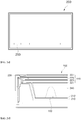
- FIG. 1A and FIG. 1B are a top view and a bottom view of a display apparatus according to a first exemplary embodiment of the present disclosure, respectively, and FIG. 2A and FIG. 2B are cross-sectional views of the display apparatus according to the first exemplary embodiment of the present disclosure.
- a display apparatus 200 includes light emitting diode packages 100, a front cover 230, a frame 210, an optical part 220, and a light guide plate 240.
- Each of the light emitting diode packages 100 includes a light emitting diode chip 112, a reflector 114, and a molding part 116, which will be described below.
- the front cover 230 may cover part of side and upper surfaces of a display panel 227 of the optical part 220.
- the front cover 230 may have a hollow center and the display panel 227 may be disposed at the center of the front cover 230 such that an image displayed on the display panel 227 can be viewed outside the display apparatus.
- the frame 210 may support the display apparatus 200 and may be coupled to one side of the front cover 230.
- the frame 210 may be formed of a synthetic resin or a metallic material such as Al alloys.
- the frame 210 may be separated a predetermined distance from the optical part 220.
- the light emitting diode package 100 may be disposed on the frame 210 so as to face the optical part 220.
- a distance between the frame 210 and the optical part 220 may be an optical distance (OD) from the light emitting diode package 100to the optical part 220.
- the optical distance (OD) may be, for example, about 1 mm to 15 mm.
- the frame 210 may be provided at an upper side thereof with a substrate 212, to which the light emitting diode package 100 is electrically connected.
- the substrate 212 serves to allow power supply to the light emitting diode package 100 therethrough.
- the optical part 220 is disposed above the frame 210, and includes a phosphor sheet 221, a diffusion plate 223, an optical sheet 225 and the display panel 227.
- the phosphor sheet 221 serves to perform wavelength conversion of light emitted from the light emitting diode package 100.
- the phosphor sheet 221 may contain at least one type of phosphor and may further include at least one type of quantum dot (QD).
- QD quantum dot
- the light emitting diode package 100 may emit blue light or UV light, and light emitted through the phosphor sheet 221 may be white light.
- the diffusion plate 223 serves to diffuse light in an upward direction upon receiving the light from the light emitting diode package 100.
- the optical sheet 225 may be disposed on the diffusion plate 223 and the display panel 227 may be disposed on the optical sheet 225.
- the optical sheet 225 may include a plurality of sheets having different functions.
- the optical sheet 225 may include one or more prism sheets and diffusion sheets.
- the diffusion sheet can provide more uniform brightness by preventing light emitted through the diffusion plate 223 from being partially collected.
- the prism sheet can collect light emitted through the diffusion sheet to allow the light to enter the display panel 227 at a right angle.
- the display panel 227 is disposed on an upper surface of the display apparatus 200 and displays an image.
- the display panel 227 includes a plurality of pixels and can output an image corresponding to a color, brightness and chroma of each pixel.
- the light guide plate 240 is interposed between the frame 210 and the optical part 220.
- the light guide plate 240 serves to allow uniform emission of light towards the optical part 220 upon receiving light.
- the thickness of the light guide plate 240 may be the same as an optical distance (OD), which is a distance between the frame 210 and the optical part 220, or may be smaller than the OD. That is, the optical distance corresponding to the distance from light emitting diode package 100 to the optical part 220 may be determined depending upon the thickness of the light guide plate 240.
- an air gap may be formed between the light guide plate 240 and the optical part 220.
- the light emitting diode package 100 is disposed on the frame 210 and the light guide plate 240 is disposed above the light emitting diode package 100.
- the light guide plate 240 has a lower surface directly contacting the frame 210 and may be formed with a light source groove h placed corresponding to a location of the light emitting diode package 100. Accordingly, light emitted from the light emitting diode package 100 enters the light guide plate 240 through the light source groove h.
- the light source groove h may have a concave shape and the shape of the light source groove h can be modified as needed. This will be described below.
- the number of light source grooves h may correspond to the number of light emitting diode packages 100.
- the display apparatus 200 includes a plurality of light emitting diode packages 100 regularly arranged thereon.
- the light emitting diode packages 100 may be arranged in a matrix to be separated at constant intervals from each other.
- FIG. 1A shows the structure wherein a plurality of light emitting diode packages 100 is regularly arranged.
- the display apparatus 200 can provide higher quality of HDR (high dynamic range) with increasing number of light emitting diode packages 100.
- the display apparatus may be provided with a plurality of power supply units 250, which supply electric power to the plurality of light emitting diode packages 100.
- Each power supply unit 250 can supply power to at least one light emitting diode package 100.
- electric power is supplied to 32 light emitting diode packages 100 through one power supply unit 250.
- the plurality of light emitting diode packages 100 can emit light and be individually operated.
- FIG. 3 is a sectional view of a light guide plate of the display apparatus according to the first exemplary embodiment of the present disclosure.
- the light guide plate 240 of the display apparatus 200 will be described in more detail with reference to FIG. 3 .
- a plurality of light emitting diode packages 100 is disposed on the frame 210, and a relationship between one of the light emitting diode packages 100 and the light guide plate 240 will be described together with the shape of the light guide plate 240.
- the light guide plate 240 is interposed between the frame 210 and the optical part 220 and has a predetermined area to be disposed over the entirety of the display apparatus 200.
- the light guide plate 240 has a substantially flat upper surface and may have a roughness R on the upper surface thereof, as needed.
- the roughness R formed on the upper surface of the light guide plate 240 serves to diffuse light when the light is discharged through the light guide plate 240.
- the roughness R may be formed in a predetermined pattern or may be formed in an irregular diffusion pattern.
- the irregular diffusion pattern may be formed through corrosion treatment with respect to the upper surface of the light guide plate 240.
- the light guide plate 240 may be formed at a lower side thereof with the light source grooves h.
- the number of light source grooves h may correspond to the number of light emitting diode packages 100 and each of the light source grooves may have a concave shape.
- the light source groove may be configured to diffuse light in a lateral direction of the light source groove h when the light enters the light source groove h.
- the depth of the light source groove h may be larger than the width thereof.
- the light source groove h may have a width gradually decreasing from a lower surface of the light guide plate 240 to an upper surface thereof and may have a concave upper surface, without being limited thereto.
- the light source groove h may have a flat upper surface. That is, the light source groove h may have a bell-shaped cross-section.
- the light guide plate 240 may have a thickness t1 of 0.5 mm to 3.0 mm and the light source groove h may have a depth t2 corresponding to about 70% to about 80% of the thickness of the light guide plate 240.
- the depth t2 of the light source groove h may be about 0.9 mm.
- the roughness R may have a thickness t3 of 5 ⁇ m to 500 ⁇ m, for example, about 170 ⁇ m.
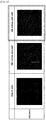
- FIG. 4 is a graph comparing light emission through the light guide plate 240 when light is emitted from the light emitting diode packages according to the first exemplary embodiment of the present disclosure.
- images of light emitted from the light emitting diode packages 100 without passing through the light guide plate 240 are compared with images of light emitted from the light emitting diode packages 100 and passing through the light guide plate 240.
- FIG. 4 shows images of light emitted from nine light emitting diode packages 100, in which the OD is set to 2.8 mm.
- FIG. 4 which shows distribution of light emitted from the nine light emitting diode packages without passing through the light guide plate, it can be confirmed that the light emitted from the light emitting diode packages 100 is not spread and a spot is generated at each of the locations of the light emitting diode packages 100.
- FIG. 4 which shows distribution of light emitted from the nine light emitting diode packages and passing through the light guide plate 240 having a thickness of 1.5 mm, it can be confirmed that the light emitted from the light emitting diode packages 100 is more uniformly spread than the light shown in the left image and spots are partially generated at the locations of the light emitting diode packages 100.
- FIG. 4 which shows distribution of light emitted from the nine light emitting diode packages and passing through the light guide plate 240 having a thickness of 2.8 mm, which is the same as the optical distance (OD), it can be confirmed that the light is more uniformly spread than the light shown in the left and middle images.
- the light guide plate 240 spreads the light around the light emitting diode packages 100, whereby the light can be uniformly discharged through a light exit surface of the light guide plate 240.
- FIG. 5 is a sectional view of the light emitting diode package of the display apparatus according to the first exemplary embodiment of the present disclosure.
- the light emitting diode package 100 includes a light emitting diode chip 112, a reflector 114, and a molding part 116.
- the light emitting diode chip 112 may include an n-type semiconductor layer, an active layer, and a p-type semiconductor layer.
- each of the n-type semiconductor layer, the active layer and the p-type semiconductor layer may include a Group III-V-based compound semiconductor.
- each of the n-type semiconductor layer, the active layer and the p-type semiconductor layer may include a nitride semiconductor such as (Al, Ga, In)N.
- the n-type semiconductor layer may be a conductive semiconductor layer containing n-type dopants (for example, Si) and the p-type semiconductor layer may be a conductive semiconductor layer containing p-type dopants (for example, Mg).
- the active layer is interposed between the n-type semiconductor layer and the p-type semiconductor layer, and may have a multi-quantum well (MQW) structure.
- the composition of the active layer may be determined so as to emit light having a desired peak wavelength.
- the light emitting diode chip 112 may be a flip-chip type light emitting diode chip 112.
- the light emitting diode chip 112 may be provided at a lower side thereof with an n-type electrode electrically connected to the n-type semiconductor layer and a p-type electrode electrically connected to the p-type semiconductor layer.
- the light emitting diode chip 112 When light is emitted from the light emitting diode chip 112, the light is emitted through upper and side surfaces of the light emitting diode chip 112.
- the light emitting diode chip 112 may have a size of, for example, 670 ⁇ m x 670 ⁇ m x 250 ⁇ m (length x width x thickness).
- the reflector 114 may be disposed on the light emitting diode chip 112 so as to cover the entirety of an upper surface of the light emitting diode chip 112.
- the reflector 114 may reflect light emitted from the light emitting diode chip 112 or may allow some fractions of light emitted from the light emitting diode chip 112 to be transmitted therethrough while reflecting the remaining fraction of the light.
- the reflector 114 may include a distributed Bragg reflector (DBR).
- the distributed Bragg reflector may be formed by alternately stacking material layers having different indices of refraction.
- the distributed Bragg reflector can reflect the entirety or part of light emitted from the light emitting diode chip 112 depending upon the number of material layers constituting the distributed Bragg reflector.
- the reflector 114 may include a metal or other materials, instead of the distributed Bragg reflector, as needed.
- the reflector 114 may have a light transmittance of 0% to 80%.
- the distributed Bragg reflector may be formed through molecular beam epitaxy, E-beam evaporation, ion-beam assisted deposition, reactive plasma deposition, or sputtering.
- the molding part 116 may be disposed to cover the entirety of the light emitting diode chip 112, on which the reflector 114 is disposed. That is, the molding part 116 may be disposed to cover the upper and side surfaces of the light emitting diode chip 112 excluding the n-type electrode and the p-type electrode disposed on the lower side of the light emitting diode chip 112.
- the molding part 116 may be formed of a transparent material, for example, silicone, so as to allow light emitted from the light emitting diode chip 112 to pass therethrough.
- the molding part 116 is formed to cover the light emitting diode chip 112 and may have a size of, for example, 1,500 ⁇ m x 1,500 ⁇ m x 420 ⁇ m (length x width x thickness). That is, the thickness of the molding part 116 may be larger than or the same as the sum of a thickness t of the light emitting diode chip 112 and a thickness d1 (hereinafter, first thickness) of the molding part 116 from the upper surface of the light emitting diode chip 112 to an upper surface of the molding part 116.
- the first thickness d1 of the molding part 116 may be smaller than or the same as the thickness t of the light emitting diode chip 112 (d1 ⁇ t).
- a width d2 (hereinafter, first width) of the molding part 116 from a side surface of the light emitting diode chip 112 to a side surface of the molding part 116 may be smaller than the first thickness d1.
- the first width d2 of the molding part 116 may be 1.5 times to 4 times, for example, about 2.44 times the first thickness d1.
- the molding part 116 is formed such that the thickness d1 of the molding part 116 formed on the upper surface of the light emitting diode chip 112 is smaller than the width d2 of the molding part 116 formed on the side surface of the light emitting diode chip 112.
- Light emitted from the light emitting diode chip 112 is blocked by the reflector disposed on the upper surface of the light emitting diode chip and can be mostly emitted in the lateral direction of the light emitting diode chip 112.
- light emitted from the light emitting diode chip 112 is guided by the shape of the molding part 116 formed on the upper and side surfaces of the light emitting diode chip 112 to be more efficiently discharged in the lateral direction.
- the light emitting diode package 100 including the molding part 116 formed to cover the light emitting diode chip 112 allows light emitted from the light emitting diode chip 112 to be discharged through the side surface thereof rather than the upper surface thereof, the light emitting diode package can be used as a light source for a backlight unit of the display apparatus 200. Furthermore, when light is emitted from the light emitting diode package 100, the light is refracted in the lateral direction while passing through the light guide plate 240, thereby providing uniform light throughout the display panel 227 of the display apparatus 200.
- the light emitting diode package 100 allows light to be discharged in the lateral direction thereof, it is possible to omit a lens for diffusing light.
- the light source groove h of the light guide plate 240 can act as a lens.
- the lens serves to spread light in the lateral direction upon receiving light from the light emitting diode package 100.
- the light since the light is spread in the lateral direction of the light emitting diode package 100 when the light enters the light guide plate 240 through the light source groove h of the light guide plate 240, it is possible to omit a separate lens.
- the display apparatus 200 since the display apparatus 200 according to this first exemplary embodiment does not employ a separate lens, it is possible to minimize the thickness of the display apparatus.
- the molding part 116 may be formed of a transparent material alone, or may further include at least one type of phosphor or at least one type of light diffuser for regulating light diffusion.
- the molding part 116 since the optical part 220 includes the phosphor sheet 221 as described above, the molding part 116 can omit a separate phosphor.
- the molding part 116 may contain at least one type of phosphor.
- the light emitting diode package 100 is illustrated as including the light emitting diode chip 112, the reflector 114 and the molding part 116. Alternatively, at least one of the reflector 114 and the molding part 116 may be omitted.
- the light emitting diode package 100 may include the light emitting diode chip 112 alone such that the light emitting diode chip 112 is disposed in the light source groove h of the light guide plate 240. With this structure, light emitted from the light emitting diode chip 112 can be spread in the lateral direction through the light guide plate 240.
- the light emitting diode package 100 may include the light emitting diode chip 112 and the reflector 114 without the molding part.
- the reflector 114 can increase the amount of light discharged in the lateral direction by reflecting more light in the lateral direction than in the upward direction when the light is emitted from the light emitting diode chip 112.
- FIG. 6 is a graph comparing light emission from the light emitting diode package according to the first exemplary embodiment of the present disclosure.
- FIG. 6 shows images and beam angles of light emitted from the light emitting diode package according to the first exemplary embodiment of the present disclosure.
- FIG. 6(a) shows far field data of images of light emitted from the light emitting diode chip 112 and photographed at an OD of 0.4 mm, at an OD of 4 mm and at an OD of 50 cm, respectively.
- FIG. 6(b) shows far field data of images of light emitted from the light emitting diode chip 112 with the reflector 114 disposed on the upper side thereof, and photographed at an OD of 0.4 mm, at an OD of 4 mm and at an OD of 50 cm, respectively.
- FIG. 6(b) shows far field data of images of light emitted from the light emitting diode chip 112 with the reflector 114 disposed on the upper side thereof, and photographed at an OD of 0.4 mm, at an OD of 4 mm and at an OD of 50 cm, respectively.
- FIG. 6(a) shows
- 6(c) shows far field data of images of light emitted from the light emitting diode chip 112 with the reflector 114 and the molding part 116 disposed thereon, and photographed at an OD of 0.4 mm, at an OD of 4 mm and at an OD of 50 cm, respectively.
- the reflector 114 and the molding part 116 formed on the light emitting diode chip 112 allow uniform spreading of light emitted from the light emitting diode package 100.
- FIG. 7 is a sectional view of a light guide plate of a display apparatus according to a second exemplary embodiment of the present disclosure.
- a display apparatus 200 includes a light emitting diode package 100, a front cover 230, a frame 210, an optical part 220, a light guide plate 240, and a reflection sheet 260.
- descriptions of the same components as those of the first exemplary embodiment will be omitted.
- the light guide plate 240 is interposed between the frame 210 and the optical part 220 and serves to achieve uniform emission of light towards an upper surface 247 of the light guide plate 240 by spreading light emitted from a plurality of light emitting diode packages 100 disposed on the frame 210 in the lateral direction.
- the light guide plate 240 is provided at a lower side thereof with light source grooves h each receiving the light emitting diode package 100.
- the number of light source grooves h may correspond to the number of light emitting diode packages 100 and each of the light sources h may have a concave shape.
- the concave shape of the light source groove is formed to spread light emitted from the light emitting diode package 100 to a plane direction of the light guide plate 240 and may have a bell shape, as shown in FIG. 7 , or other shapes as needed.
- the depth and width of the light source groove h may be the same as those of the light source groove h of the light guide plate according to the first exemplary embodiment, the depth of the light source groove h according to this exemplary embodiment may be smaller than the depth of the light source groove according to the first exemplary embodiment.
- This structure results from the structure of the light guide plate having light exit grooves Eh formed above the light source grooves h.
- Each of the light exit grooves Eh is formed above the light source groove h and the number of light exit grooves Eh corresponds to the number of light source grooves h.
- the light exit grooves Eh may have a conical shape and have a larger width than the light source grooves h.
- the width of the light exit groove Eh may be larger than the depth thereof.
- Each of the light exit grooves Eh serves to reflect light on an inner surface thereof to spread in the lateral direction (plane direction) of the light guide plate 240 when the light emitted from the light emitting diode package 100 enters the light guide plate 240 through the light source groove h.
- an inner tip (vertex of the conical shape) of the light exit groove (Eh) may have a gently curved surface instead of a sharp shape, or may have a flat surface as needed.
- the light exit groove Eh is shown as having a linear inclined surface 245 in the cross-sectional view of FIG. 7
- the light exit groove Eh may have a concave inclined surface as shown in the inclined surface 245 of the light source groove h, or a convex inclined surface as needed.
- the uppermost end of the light exit groove Eh extends to the upper surface 247 of the light guide plate 240.
- the upper surface 247 of the light guide plate 240 may be a light exit surface through which the light exits the light guide plate 240.
- the upper surface 247 of the light guide plate 240 may be a substantially flat surface, without being limited thereto.
- the upper surface 247 of the light guide plate 240 may not be flat or may have a roughness as needed.
- the light guide plate has the light exit grooves Eh formed above light source grooves h as described above, light emitted from the light emitting diode package 100 is spread over the light guide plate 240 to be uniformly discharged through the upper surface 247 of the light guide plate 240.
- the reflection sheet 260 may be disposed on the lower surface of the light guide plate 240.
- the reflection sheet 260 serves to increase the amount of light discharged through the upper surface of the light guide plate 240 when the light enters the light guide plate 240.
- the reflection sheet 260 may have a thickness of, for example, about 120 ⁇ m to 250 ⁇ m, which is similar to the thickness (for example, 150 ⁇ m to 350 ⁇ m) of the light emitting diode package 100.
- the reflection sheet 260 may be separated from the light emitting diode package 100 by a predetermined distance or more in order to prevent light emitted from the light emitting diode package 100 from being lost through reflection by a side surface of the reflection sheet 260.
- the lower surface of the light guide plate 240 has a step due to the thickness of the reflection sheet 260. That is, the lower surface of the light guide plate 240 includes a first lower surface 241 and a second lower surface 243, and the step is formed between the first lower surface 241 and the second lower surface 243.
- the first lower surface 241 may adjoin the substrate 212 on which the light emitting diode chip 112 is disposed, and the second lower surface 243 may adjoin the reflection sheet 260. As such, the step is formed between the second lower surface 243 and the first lower surface 241 due to the thickness of the reflection sheet 260.
- the first lower surface 241 may extend from a distal end of the light source groove h and an inclined surface 245 may be formed between the first lower surface 241 and the second lower surface 243.
- the inclined surface 245 serves to connect both ends of the step formed between the first lower surface 241 and the second lower surface 243.
- the light guide plate may include the inclined surface 245 directly extending from the distal end of the light source groove h to the second lower surface 243 by omitting the first lower surface 241, as needed.
- the light guide plate 240 when light emitted from the light emitting diode chip 112 received in the light source groove h of the light guide plate 240 on the substrate 212 enters the light guide plate 240 through the light source groove h, the light can be discharged through the upper surface 247 of the light guide plate 247 while being reflected by some portions of the light guide plate 240 to spread in the lateral direction of the light guide plate 240.
- the light exit grooves Eh formed on the light guide plate 240 and placed corresponding to the light source groove h can improve efficiency of spreading light in the lateral direction of the light guide plate 240.
- the reflection sheet 260 disposed on the lower surface of the light guide plate 240 can increase the amount of light discharged through the upper surface 247 of the light guide plate 240.
- the light emitting diode chip 112 may be separated from the reflection sheet 260 by a predetermined distance or more.
- the light source groove h and the inclined surface 245 of the light guide plate 240 are disposed between the light emitting diode chip 112 and the reflection sheet 260 to prevent light emitted from the light emitting diode chip 112 from directly reaching the side surface of the reflection sheet 260, thereby minimizing loss of light through reflection by the side surface of the reflection sheet 260.
- FIG. 8 shows simulation images of light emitted from the display apparatus according to the second exemplary embodiment of the present disclosure.
- FIG. 8 shows simulation results as to uniformity of light discharged from the display apparatus 200 according to the second exemplary embodiment of the present disclosure, in which the light emitting diode packages 100 are disposed.
- the light guide plate 240 and the reflection sheet 260 according to this exemplary embodiment were disposed on the light emitting diode packages 100, and the light guide plate 240 was coved only by a brightness enhancement film (BEF) and a diffusion sheet.
- BEF brightness enhancement film
- FIG. 8 shows only part of the display apparatus.
- the display apparatus generally had a light distribution of 9.56E+03 or more and the light distribution had a substantially linear shape both in the x-axis direction and in the y-axis direction.
- the intensity of light was maintained at a certain level or higher and the light was generally uniformly discharged through the display apparatus.
- light emitted from the light emitting diode packages 100 can be uniformly spread in the light guide plate 240 and thus can be uniformly discharged as surface light through the upper surface 247 of the light guide plate 240, which is the light exit surface.
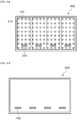
- FIG. 9A and FIG. 9B are a top view and a bottom view of a display apparatus according to one exemplary embodiment of the present disclosure, respectively, and FIG. 10A and FIG. 10B are cross-sectional views of the display apparatus according to the exemplary embodiment of the present disclosure.
- a display apparatus 200 includes light emitting diode packages 100, a front cover 230, a frame 210, an optical part 220, and lenses 300.
- Each of the light emitting diode packages 100 includes a light emitting diode chip 112, a reflector 114, and a molding part 116, which will be described below.
- the front cover 230 may cover part of side and upper surfaces of a display panel 227 of the optical part 220.
- the front cover 230 may have a hollow center and the display panel 227 may be disposed at the center of the front cover 230 such that an image displayed on the display panel 227 can be viewed outside the display apparatus.
- the frame 210 may support the display apparatus 200 and may be coupled at one side thereof to the front cover 230.
- the frame 210 may be formed of a synthetic resin or a metallic material such as an Al alloy.
- the frame 210 may be separated a predetermined distance from the optical part 220.
- the light emitting diode package 100 may be disposed on the frame 210 so as to face the optical part 220.
- a distance between the frame 210 and the optical part 220 may be an optical distance (OD) from the light emitting diode package 100 to the optical part 220.
- the optical distance (OD) may be, for example, about 1 mm to 15 mm.
- the frame 210 may be provided at an upper side thereof with a substrate 212, to which the light emitting diode package 100 is electrically connected.
- the substrate 212 serves to allow power supply to the light emitting diode package 100 therethrough.
- the optical part 220 is disposed above the frame 210, and includes a phosphor sheet 221, a diffusion plate 223, an optical sheet 225 and the display panel 227.
- the phosphor sheet 221 serves to perform wavelength conversion of light emitted from the light emitting diode package 100.
- the phosphor sheet 221 may contain at least one type of phosphor and may further include at least one type of quantum dot (QD).
- QD quantum dot
- the light emitting diode package 100 may emit blue light or UV light, and light emitted through the phosphor sheet 221 may be white light.
- the diffusion plate 223 serves to diffuse light in an upward direction upon receiving the light from the light emitting diode package 100.
- the optical sheet 225 may be disposed on the diffusion plate 223 and the display panel 227 may be dispose on the optical sheet 225.
- the optical sheet 225 may include a plurality of sheets having different functions.
- the optical sheet 225 may include one or more prism sheets and diffusion sheets.
- the diffusion sheet can provide more uniform brightness by preventing light emitted through the diffusion plate 223 from being partially collected.
- the prism sheet can collect light emitted through the diffusion sheet to allow the light to enter the display panel 227 at a right angle.
- the display panel 227 is disposed on an upper surface of the display apparatus 200 and displays an image.
- the display panel 227 includes a plurality of pixels and can output an image corresponding to a color, brightness and chroma of each pixel.
- the display apparatus may be provided with a plurality of power supply units 250, which supply electric power to the plurality of light emitting diode packages 100.
- Each power supply unit 250 can supply power to at least one light emitting diode package 100.
- electric power is supplied to 32 light emitting diode packages 100 through one power supply unit 250.
- the plurality of light emitting diode packages 100 can emit light and be individually operated.
- each of the lenses 300 is disposed on the frame 210 between the frame 210 and the optical part 220.
- the lens 300 serves to guide light emitted from the light emitting diode package 100 to travel in a lateral direction of the lens 300. This structure will be described in detail with reference to FIG. 11 .
- FIG. 11 is a sectional view of a lens of the display apparatus according to the exemplary embodiment of the present disclosure.
- the lens 300 shown in FIG. 11 is provided for illustration only and the shape of the lens 300 can be modified, as needed.
- An optical distance (OD) corresponding to a distance from the frame 210 to the optical part 220 can be adjusted depending upon the height of the lens 300.
- the lens 300 is disposed on the frame 210 such that an upper surface 350 of the lens 300 closely adjoins the optical part 220.
- an air gap may be formed between the upper surface 350 of the lens 300 and the optical part 220. That is, the OD can be adjusted as needed.
- the lens 300 includes a lower surface 310, an upper surface 350, a flange 370, and legs 390.
- the lower surface 310 may include a concave portion 320 and an inclined surface surrounding the concave portion 320.
- a flat surface may be disposed between the concave portion 320 and the inclined surface, as needed.
- the inclined surface serves to allow light emitted from the light emitting diode package 100 and entering the lens 300 to be discharged through a side surface of the lens 300 without total internal reflection, and an inclination of the inclined surface depends upon the shape of the lens 300.
- the concave portion 320 defines a light incident face 330 through which light emitted from the light emitting diode package 100 enters the lens 300. That is, the light incident face 330 is an inner surface of the concave portion 320 and includes a side surface 330a and an upper end portion 330b.
- the concave portion 320 has a shape gradually decreasing in width from an entrance thereof in an upward direction.
- the side surface 330a may have a constant inclination from the entrance of the concave portion 320 to the upper end portion 330b.
- the side surface 330a may have an inclination gradually decreasing from the entrance of the concave portion 320 to the upper end portion 330b. That is, the side surface 330a may have a convex shape, as shown in FIG. 11 .
- the upper end portion 330b may include a concave surface or may have a flat surface, as needed.
- Height of the concave portion 320 may be adjusted depending upon a beam angle of the light emitting diode package 100, the shape of the upper surface 350 of the lens 300, directional distribution of light, and the like.
- the upper surface 350 of the lens 300 is configured to allow light having entered the lens 300 to spread in a wide directional distribution, and acts as a light exit surface through which light exits the lens 300.
- the upper surface 350 of the lens 300 may include a concave surface 350a near a central axis of the lens 300 and a convex surface 350b extending from the concave surface 350a.
- the concave surface 350a guides light traveling near the central axis of the lens 300 to be directed outwards, and the convex surface 350b increases the amount of light traveling outward from the central axis of the lens 300.
- the flange 370 connects the upper surface 350 to the lower surface 310 and defines the size of the lens 300.
- a side surface of the flange 370 and the lower surface 310 may have a roughened pattern, as needed.
- the legs 390 of the lens 300 are coupled to the frame 210 to secure the lens 300.
- a leading end of each leg 390 may be bonded to the frame 210 by a bonding agent and the like.
- the light emitting diode package 100 described below may be disposed on the frame 210 and the lens 300 may be disposed on the light emitting diode package 100.
- the lens 300 may be disposed on the frame 210 such that the light emitting diode package 100 is placed inside the concave portion 320. With this structure, light emitted from the light emitting diode package 100 can enter the lens 300 through the light incident face 330 of the concave portion 320.
- the number of lenses 300 may be the same as the number of light emitting diode packages 100.
- the display apparatus 200 includes a plurality of light emitting diode packages 100 regularly arranged thereon.
- the light emitting diode packages 100 may be arranged in a matrix to be separated at constant intervals from each other.
- FIG. 9A shows the structure wherein a plurality of light emitting diode packages 100 is regularly arranged.
- the display apparatus 200 can provide higher quality HDR (high dynamic range) with increasing number of light emitting diode packages 100.
- FIG. 12 is a sectional view of a light emitting diode package according to one exemplary embodiment of the present disclosure.
- the light emitting diode package 100 includes a light emitting diode chip 112, a reflector 114, and a molding part 116.
- the light emitting diode chip 112 may include an n-type semiconductor layer, an active layer, and a p-type semiconductor layer.
- each of the n-type semiconductor layer, the active layer and the p-type semiconductor layer may include a Group III-V-based compound semiconductor.
- each of the n-type semiconductor layer, the active layer and the p-type semiconductor layer may include a nitride semiconductor such as (Al, Ga, In)N.
- the n-type semiconductor layer may be a conductive semiconductor layer containing n-type dopants (for example, Si) and the p-type semiconductor layer may be a conductive semiconductor layer containing p-type dopants (for example, Mg).
- the active layer is interposed between the n-type semiconductor layer and the p-type semiconductor layer, and may have a multi-quantum well (MQW) structure.
- the composition of the active layer may be determined so as to emit light having a desired peak wavelength.
- the light emitting diode chip 112 may be a flip-chip type light emitting diode chip 112. With this structure, the light emitting diode chip 112 may be provided at a lower side thereof with an n-type electrode electrically connected to the n-type semiconductor layer and a p-type electrode electrically connected to the p-type semiconductor layer. When light is emitted from the light emitting diode chip 112, the light is emitted through upper and side surfaces of the light emitting diode chip 112.
- the reflector 114 may be disposed on the light emitting diode chip 112 so as to cover the entirety of an upper surface of the light emitting diode chip 112.
- the reflector 114 may reflect light emitted from the light emitting diode chip 112 or may allow some fractions of light emitted from the light emitting diode chip 112 to be transmitted therethrough while reflecting the remaining fraction of the light.
- the reflector 114 may include a distributed Bragg reflector (DBR).
- the distributed Bragg reflector may be formed by alternately stacking material layers having different indices of refraction.
- the distributed Bragg reflector can reflect the entirety or part of light emitted from the light emitting diode chip 112 depending upon the number of material layers constituting the distributed Bragg reflector.
- the reflector 114 may include a metal or other materials, instead of the distributed Bragg reflector, as needed.
- the reflector 114 may have a light transmittance of higher than 0% to less than 100%, for example, higher than 0% to 95%.
- the distributed Bragg reflector may be formed through molecular beam epitaxy, E-beam evaporation, ion-beam assisted deposition, reactive plasma deposition, or sputtering.
- the molding part 116 may be disposed to cover the entirety of the light emitting diode chip 112, on which the reflector 114 is disposed. That is, the molding part 116 may be disposed to cover the upper and side surfaces of the light emitting diode chip 112 excluding the n-type electrode and the p-type electrode disposed on the lower side of the light emitting diode chip 112.
- the molding part 116 may be formed of a transparent material, for example, silicone, so as to allow light emitted from the light emitting diode chip 112 to pass therethrough.
- the molding part 116 may be formed of a transparent material alone, or may further include at least one type of phosphor or at least one type of light diffuser for regulating light diffusion.
- the molding part 116 since the optical part 220 includes the phosphor sheet 221 as described above, the molding part 116 can omit a separate phosphor.
- the molding part 116 may contain at least one type of phosphor.
- the light emitting diode package 100 is illustrated as including the light emitting diode chip 112, the reflector 114 and the molding part 116. Alternatively, at least one of the reflector 114 and the molding part 116 may be omitted.
- the light emitting diode package 100 may include the light emitting diode chip 112 alone such that the light emitting diode chip 112 is disposed in the concave portion 320 of the lens 300.
- the light emitting diode package 100 may include the light emitting diode chip 112 and the reflector 114 without the molding part.
- the reflector 114 can increase the amount of light discharged in the lateral direction by reflecting more light in the lateral direction than in the upward direction when the light is emitted from the light emitting diode chip 112.
- FIG. 13 shows an image of light emitted from a plurality of light emitting diode packages, explaining uniformity of light emitted from the display apparatus according to the exemplary embodiment of the present disclosure.
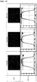
- FIG. 14 shows images and graphs comparing uniformity of light emitted from the display apparatus according to the exemplary embodiment of the present disclosure depending upon structure of light emitting diode packages and
- FIG. 15 shows graphs comparing directional characteristics of light emitted from the display apparatus according to the exemplary embodiment of the present disclosure depending upon structure of light emitting diode packages.
- FIG. 14 shows uniformity of light emitted from the display apparatus depending upon the structure of the light emitting diode packages 100.
- the first image and graph show results measured using a structure wherein the light emitting diode chip 112 not including the reflector 114 is disposed in the concave portion 320 of the lens 300 and the optical part 220 including the diffusion sheet 223 and the phosphor sheet 221 is disposed above the lens 300.
- the second image and graph show results measured using a structure wherein the light emitting diode package 100 including the reflector 114 having a reflectivity of 70% and disposed on the light emitting diode chip 112 is disposed in the concave portion 320 of the lens 300 and the optical part 220 including the diffusion sheet 223 and the phosphor sheet 221 is disposed above the lens 300.
- the third image and graph show results measured using a structure wherein the light emitting diode package 100 including the reflector 114 having a reflectivity of 95% and disposed on the light emitting diode chip 112 is disposed in the concave portion 320 of the lens 300 and the optical part 220 including the diffusion sheet 223 and the phosphor sheet 221 is disposed above the lens 300.
- the light emitting diode package 100 including the reflector 114 having a reflectivity of 95% provided a uniformity degree of 95%, which was about 6% higher than the light emitting diode package 100 not including the reflector 114.
- the light emitting diode package 100 including the reflector 114 having a reflectivity of 95% exhibited better spreading of light in the lateral direction than the light emitting diode package 100 not including the reflector 114.
- the light emitting diode package 100 including the reflector 114 provided high light distribution efficiency, the light distribution efficiency of the light emitting diode package 100 could be further improved through the lens 300 coupled thereto.
Landscapes
- Physics & Mathematics (AREA)
- Nonlinear Science (AREA)
- General Physics & Mathematics (AREA)
- Optics & Photonics (AREA)
- Mathematical Physics (AREA)
- Chemical & Material Sciences (AREA)
- Crystallography & Structural Chemistry (AREA)
- Engineering & Computer Science (AREA)
- Microelectronics & Electronic Packaging (AREA)
- Planar Illumination Modules (AREA)
Abstract
Description
- Exemplary embodiments of the present disclosure relate to a display apparatus and a backlight unit thereof, and more particularly, to a display apparatus emitting light through a direct type backlight and a backlight unit thereof.
- Recently, there is increasing demand for making a display apparatus as thin as possible. Accordingly, for a liquid crystal display (LCD), an edge type backlight unit including a light source disposed at one side thereof is generally used.
- However, a liquid crystal display including such an edge type backlight unit cannot realize high dynamic range (HDR) imaging, which is a method of producing images on a display screen so as to allow a viewer to experience a sense of viewing an actual scene through the images. In order to realize HDR, it is necessary to realize a difference in luminance of light emitted through the display apparatus depending upon locations on a display screen. However, the liquid crystal display employing the edge type backlight unit cannot realize a difference in luminance of light depending upon locations on the display screen.
- Accordingly, various studies have been made to realize HDR through implementation of an active matrix type using a direct type backlight unit. One example of these studies is disclosed in Korean Patent Laid-open Publication No.
10-2016-0051566 - Although a backlight unit employs a lens in order to realize uniform surface light throughout the backlight unit by allowing light emitted from the light emitting diode to spread in the lateral direction, it is difficult to improve uniformity of a surface light source even using the lens.
- Exemplary embodiments of the present disclosure provide a display apparatus that can reduce a thickness thereof while employing a direct type backlight and a backlight unit thereof.
- Exemplary embodiments of the present disclosure provide a display apparatus that can improve uniformity of a surface light source while employing a direct type backlight.
- In accordance with one aspect of the present disclosure, a display apparatus includes: a frame; a plurality of light emitting diodes regularly arranged on the frame; an optical part disposed above the plurality of light emitting diodes and including a display panel and at least one of a phosphor sheet and an optical sheet; and a light guide plate disposed between the frame and the optical part to cover the plurality of light emitting diodes, wherein the light guide plate is formed with light source grooves placed corresponding to locations of the plurality of light emitting diodes, respectively, such that light emitted from each of the light emitting diodes enters the corresponding light source groove.
- The light source groove may have a concave shape and include a flat upper surface.
- The light guide plate may include a regular or irregular roughness formed on an upper surface thereof. The roughness may have a thickness of 5 µm to 500 µm.
- The light guide plate may have a thickness of 0.5 mm to 3.0 mm and the light source groove may have a depth corresponding to 70% to 80% of a thickness of the light guide plate.
- Each of the light emitting diodes may be a light emitting diode chip.
- Each of the light emitting diodes may be a light emitting diode package. Here, the light emitting diode package may include a light emitting diode chip; and a reflector disposed on an upper surface of the light emitting diode chip and reflecting at least part of light emitted from the light emitting diode chip. The reflector may include a distributed Bragg reflector. The reflector may have a transmittance of 0% to 80% with respect to light emitted from the light emitting diode chip.
- The light emitting diode package may further include a molding part disposed to cover upper and side surfaces of the light emitting diode chip and the reflector.
- The molding part may have a smaller thickness from the upper surface of the reflector to an upper surface of the molding part than a width from the side surface of the light emitting diode chip to a side surface of the molding part.
- The width of the molding part from the side surface of the light emitting diode chip to the side surface of the molding part may be 1.5 to 4 times the thickness of the molding part from the upper surface of the reflector to the upper surface of the molding part.
- The molding part may include at least one of at least one type of phosphor and at least one type of light diffuser.
- The light guide plate may have a light exit groove formed on an upper surface thereof and having a concave shape. The light exit groove may have a conical shape.
- The display apparatus may further include a reflection sheet interposed between the light guide plate and the frame and reflecting light inside the light guide plate in an upward direction. The reflection sheet may be separated from the light emitting diode package.
- The light guide plate may have a lower surface stepped from a distal end of the light source groove and an inclined surface between the light source groove and the lower surface, and the lower surface may adjoin the reflection sheet.
- The lower surface may be a second lower surface and the light guide plate may further include a first lower surface between the inclined surface and the light source groove.
- In accordance with another aspect of the present disclosure, a backlight unit of a display apparatus includes: a plurality of light emitting diodes; and a light guide plate disposed to cover the plurality of light emitting diodes and spreading light emitted from the plurality of light emitting diodes, wherein the light guide plate is formed with light source grooves placed corresponding to locations of the plurality of light emitting diodes, respectively, such that light emitted from each of the light emitting diodes enters the corresponding light source groove.
- The light source groove may include a flat upper surface and the light guide plate may include a regular or irregular roughness formed on an upper surface thereof.
- The light source groove may have a depth corresponding to 70% to 80% of a thickness of the light guide plate.
- The light guide plate may have a light exit groove formed on an upper surface thereof and having a concave shape. The light exit groove may have a conical shape.
- The backlight unit may further include a reflection sheet disposed on a lower surface of the light guide plate and reflecting light inside the light guide plate in an upward direction.
- The light guide plate may include a first lower surface extending from the light source groove, a second lower surface stepped from the first lower surface, and an inclined surface between the first lower surface and the second lower surface, and the second lower surface may adjoin the reflection sheet.
- In accordance with one aspect of the present disclosure, a display apparatus includes: a frame; a plurality of light emitting diode packages regularly arranged on the frame; an optical part disposed above the plurality of light emitting diode packages and including a display panel and at least one of a phosphor sheet and an optical sheet; and a lens disposed between the frame and the optical part to cover each of the light emitting diode packages and spreading light emitted from the corresponding light emitting diode package, wherein each of the light emitting diode packages includes a light emitting diode chip; and a reflector disposed on an upper surface of the light emitting diode chip and reflecting at least part of light emitted from the light emitting diode chip.
- The lens may include a lower surface having a concave portion defining a light incident face through which light enters the lens; and an upper surface through which light exits the lens, and the light emitting diode package may be disposed inside the concave portion of the lens.
- The light incident face of the lens may include an upper end portion and a side surface extending from the upper end portion to an entrance of the concave portion, and the concave portion may have a width gradually decreasing from the entrance thereof to the upper end portion.
- The side surface may be an inclined surface having a constant inclination from the entrance of the concave portion to the upper end portion or a curved inclined surface having a gradually decreasing inclination from the entrance of the concave portion to the upper end portion.
- The upper end portion may be a flat surface or a curved surface.
- The reflector may include a distributed Bragg reflector. The reflector may have a transmittance of higher than 0% to less than 100% with respect to light emitted from the light emitting diode chip.
- The light emitting diode package may further include a molding part disposed to cover upper and side surfaces of the light emitting diode chip and the reflector.
- The molding part may include at least one of at least one type of phosphor and at least one type of light diffuser.
- According to exemplary embodiments, a light guide plate of the backlight unit includes a light source groove placed corresponding to a location of a light emitting diode package so as to spread light in a lateral direction when the light enters the light guide plate, thereby enabling use of a direct type backlight unit without a separate lens.
- In addition, the exemplary embodiments of the present disclosure provide a thinner direct type backlight than a typical direct type backlight unit through elimination of a separate lens, thereby enabling reduction in thickness of a display apparatus.
- According to exemplary embodiments, as a backlight unit of a display apparatus, light emitting diode packages each having a reflector disposed on a light emitting diode chip are coupled to lenses, respectively, thereby improving uniformity of surface light with respect to light emitted from a plurality of light emitting diode packages.
-
-
FIG. 1 is a top view of a display apparatus according to a first exemplary embodiment of the present disclosure. -
FIG. 1B is a bottom view of the display apparatus according to the first exemplary embodiment of the present disclosure. -
FIG. 2A andFIG. 2B are cross-sectional views of the display apparatus according to the first exemplary embodiment of the present disclosure. -
FIG. 3 is a sectional view of a light guide plate of the display apparatus according to the first exemplary embodiment of the present disclosure. -
FIG. 4 is a graph comparing light emission through the light guide plate when light is emitted from light emitting diode packages according to the first exemplary embodiment of the present disclosure. -
FIG. 5 is a sectional view of a light emitting diode package of the display apparatus according to the first exemplary embodiment of the present disclosure. -
FIG. 6 is a graph comparing light emission from the light emitting diode package of the display apparatus according to the exemplary embodiment of the present disclosure. -
FIG. 7 is a sectional view of a light guide plate of a display apparatus according to a second exemplary embodiment of the present disclosure. -
FIG. 8 shows simulation images of light emitted from the display apparatus according to the second exemplary embodiment of the present disclosure. -
FIG. 9A is a top view of a display apparatus according to one exemplary embodiment of the present disclosure. -
FIG. 9B is a bottom view of the display apparatus according to the exemplary embodiment of the present disclosure. -
FIG. 10A and FIG. 10B are cross-sectional views of the display apparatus according to the exemplary embodiment of the present disclosure. -
FIG. 11 is a sectional view of a lens of the display apparatus according to the exemplary embodiment of the present disclosure. -
FIG. 12 is a sectional view of a light emitting diode package according to one exemplary embodiment of the present disclosure. -
FIG. 13 shows an image of light emitted from a plurality of light emitting diode packages, explaining uniformity of light emitted from the display apparatus according to the exemplary embodiment of the present disclosure. -
FIG. 14 shows images and graphs comparing uniformity of light emitted from the display apparatus according to the exemplary embodiment of the present disclosure depending upon structure of light emitting diode packages. -
FIG. 15 shows graphs comparing directional characteristics of light emitted from the display apparatus according to the exemplary embodiment of the present disclosure depending upon structure of light emitting diode packages. - Exemplary embodiments of the present disclosure will be described in more detail with reference to the accompanying drawings.
-
FIG. 1A andFIG. 1B are a top view and a bottom view of a display apparatus according to a first exemplary embodiment of the present disclosure, respectively, andFIG. 2A andFIG. 2B are cross-sectional views of the display apparatus according to the first exemplary embodiment of the present disclosure. - A
display apparatus 200 according to the first exemplary embodiment of the present disclosure includes light emitting diode packages 100, afront cover 230, aframe 210, anoptical part 220, and alight guide plate 240. Each of the light emitting diode packages 100 includes a light emittingdiode chip 112, areflector 114, and amolding part 116, which will be described below. - The
front cover 230 may cover part of side and upper surfaces of adisplay panel 227 of theoptical part 220. Thefront cover 230 may have a hollow center and thedisplay panel 227 may be disposed at the center of thefront cover 230 such that an image displayed on thedisplay panel 227 can be viewed outside the display apparatus. - The
frame 210 may support thedisplay apparatus 200 and may be coupled to one side of thefront cover 230. Theframe 210 may be formed of a synthetic resin or a metallic material such as Al alloys. Theframe 210 may be separated a predetermined distance from theoptical part 220. The light emittingdiode package 100 may be disposed on theframe 210 so as to face theoptical part 220. Here, a distance between theframe 210 and theoptical part 220 may be an optical distance (OD) from the light emitting diode package 100to theoptical part 220. In this exemplary embodiment, the optical distance (OD) may be, for example, about 1 mm to 15 mm. - The
frame 210 may be provided at an upper side thereof with asubstrate 212, to which the light emittingdiode package 100 is electrically connected. Thesubstrate 212 serves to allow power supply to the light emittingdiode package 100 therethrough. - The
optical part 220 is disposed above theframe 210, and includes aphosphor sheet 221, adiffusion plate 223, anoptical sheet 225 and thedisplay panel 227. - The
phosphor sheet 221 serves to perform wavelength conversion of light emitted from the light emittingdiode package 100. Thephosphor sheet 221 may contain at least one type of phosphor and may further include at least one type of quantum dot (QD). In this exemplary embodiment, the light emittingdiode package 100 may emit blue light or UV light, and light emitted through thephosphor sheet 221 may be white light. - The
diffusion plate 223 serves to diffuse light in an upward direction upon receiving the light from the light emittingdiode package 100. - The
optical sheet 225 may be disposed on thediffusion plate 223 and thedisplay panel 227 may be disposed on theoptical sheet 225. Theoptical sheet 225 may include a plurality of sheets having different functions. By way of example, theoptical sheet 225 may include one or more prism sheets and diffusion sheets. The diffusion sheet can provide more uniform brightness by preventing light emitted through thediffusion plate 223 from being partially collected. The prism sheet can collect light emitted through the diffusion sheet to allow the light to enter thedisplay panel 227 at a right angle. - The
display panel 227 is disposed on an upper surface of thedisplay apparatus 200 and displays an image. Thedisplay panel 227 includes a plurality of pixels and can output an image corresponding to a color, brightness and chroma of each pixel. - As shown in
FIG. 2A andFIG. 2B , thelight guide plate 240 is interposed between theframe 210 and theoptical part 220. Thelight guide plate 240 serves to allow uniform emission of light towards theoptical part 220 upon receiving light. The thickness of thelight guide plate 240 may be the same as an optical distance (OD), which is a distance between theframe 210 and theoptical part 220, or may be smaller than the OD. That is, the optical distance corresponding to the distance from light emittingdiode package 100 to theoptical part 220 may be determined depending upon the thickness of thelight guide plate 240. In addition, an air gap may be formed between thelight guide plate 240 and theoptical part 220. - The light emitting
diode package 100 is disposed on theframe 210 and thelight guide plate 240 is disposed above the light emittingdiode package 100. Here, thelight guide plate 240 has a lower surface directly contacting theframe 210 and may be formed with a light source groove h placed corresponding to a location of the light emittingdiode package 100. Accordingly, light emitted from the light emittingdiode package 100 enters thelight guide plate 240 through the light source groove h. - Referring to
FIG. 2A andFIG. 2B , the light source groove h may have a concave shape and the shape of the light source groove h can be modified as needed. This will be described below. The number of light source grooves h may correspond to the number of light emitting diode packages 100. - Referring to
FIG. 1A , thedisplay apparatus 200 includes a plurality of light emittingdiode packages 100 regularly arranged thereon. By way of example, the light emittingdiode packages 100 may be arranged in a matrix to be separated at constant intervals from each other. -
FIG. 1A shows the structure wherein a plurality of light emitting diode packages 100 is regularly arranged. Thedisplay apparatus 200 can provide higher quality of HDR (high dynamic range) with increasing number of light emitting diode packages 100. - In addition, the display apparatus may be provided with a plurality of
power supply units 250, which supply electric power to the plurality of light emitting diode packages 100. Eachpower supply unit 250 can supply power to at least one light emittingdiode package 100. In this exemplary embodiment, electric power is supplied to 32 light emittingdiode packages 100 through onepower supply unit 250. Upon receiving electric power from thepower supply unit 250, the plurality of light emittingdiode packages 100 can emit light and be individually operated. -
FIG. 3 is a sectional view of a light guide plate of the display apparatus according to the first exemplary embodiment of the present disclosure. Thelight guide plate 240 of thedisplay apparatus 200 will be described in more detail with reference toFIG. 3 . - Referring to
FIG. 3 , a plurality of light emitting diode packages 100 is disposed on theframe 210, and a relationship between one of the light emittingdiode packages 100 and thelight guide plate 240 will be described together with the shape of thelight guide plate 240. - The
light guide plate 240 is interposed between theframe 210 and theoptical part 220 and has a predetermined area to be disposed over the entirety of thedisplay apparatus 200. Thelight guide plate 240 has a substantially flat upper surface and may have a roughness R on the upper surface thereof, as needed. The roughness R formed on the upper surface of thelight guide plate 240 serves to diffuse light when the light is discharged through thelight guide plate 240. Thus, the roughness R may be formed in a predetermined pattern or may be formed in an irregular diffusion pattern. The irregular diffusion pattern may be formed through corrosion treatment with respect to the upper surface of thelight guide plate 240. - The
light guide plate 240 may be formed at a lower side thereof with the light source grooves h. The number of light source grooves h may correspond to the number of light emittingdiode packages 100 and each of the light source grooves may have a concave shape. The light source groove may be configured to diffuse light in a lateral direction of the light source groove h when the light enters the light source groove h. Thus, the depth of the light source groove h may be larger than the width thereof. - The light source groove h may have a width gradually decreasing from a lower surface of the
light guide plate 240 to an upper surface thereof and may have a concave upper surface, without being limited thereto. Alternatively, the light source groove h may have a flat upper surface. That is, the light source groove h may have a bell-shaped cross-section. - By way of example, the
light guide plate 240 may have a thickness t1 of 0.5 mm to 3.0 mm and the light source groove h may have a depth t2 corresponding to about 70% to about 80% of the thickness of thelight guide plate 240. For example, when thelight guide plate 240 has a thickness t1 of about 1.3 mm, the depth t2 of the light source groove h may be about 0.9 mm. - The roughness R may have a thickness t3 of 5 µm to 500 µm, for example, about 170 µm.
-
FIG. 4 is a graph comparing light emission through thelight guide plate 240 when light is emitted from the light emitting diode packages according to the first exemplary embodiment of the present disclosure. - Referring to
FIG. 4 , in order to confirm uniformity of light emitted from the light emittingdiode package 100 due to use of thelight guide plate 240 according to the first exemplary embodiment, images of light emitted from the light emittingdiode packages 100 without passing through thelight guide plate 240 are compared with images of light emitted from the light emittingdiode packages 100 and passing through thelight guide plate 240.FIG. 4 shows images of light emitted from nine light emitting diode packages 100, in which the OD is set to 2.8 mm. - Referring to a left image of
FIG. 4 , which shows distribution of light emitted from the nine light emitting diode packages without passing through the light guide plate, it can be confirmed that the light emitted from the light emitting diode packages 100 is not spread and a spot is generated at each of the locations of the light emitting diode packages 100. - Referring to a middle image of
FIG. 4 , which shows distribution of light emitted from the nine light emitting diode packages and passing through thelight guide plate 240 having a thickness of 1.5 mm, it can be confirmed that the light emitted from the light emitting diode packages 100 is more uniformly spread than the light shown in the left image and spots are partially generated at the locations of the light emitting diode packages 100. - Referring to a right image of
FIG. 4 , which shows distribution of light emitted from the nine light emitting diode packages and passing through thelight guide plate 240 having a thickness of 2.8 mm, which is the same as the optical distance (OD), it can be confirmed that the light is more uniformly spread than the light shown in the left and middle images. - That is, when light emitted from the light emitting diode packages 100 is discharged through the
light guide plate 240 as in this exemplary embodiment, thelight guide plate 240 spreads the light around the light emitting diode packages 100, whereby the light can be uniformly discharged through a light exit surface of thelight guide plate 240. -
FIG. 5 is a sectional view of the light emitting diode package of the display apparatus according to the first exemplary embodiment of the present disclosure. - Referring to
FIG. 5 , the light emittingdiode package 100 according to the first exemplary embodiment of the present disclosure will be described in more detail. As shown inFIG. 3 , the light emittingdiode package 100 includes a light emittingdiode chip 112, areflector 114, and amolding part 116. - The light emitting
diode chip 112 may include an n-type semiconductor layer, an active layer, and a p-type semiconductor layer. Here, each of the n-type semiconductor layer, the active layer and the p-type semiconductor layer may include a Group III-V-based compound semiconductor. By way of example, each of the n-type semiconductor layer, the active layer and the p-type semiconductor layer may include a nitride semiconductor such as (Al, Ga, In)N. - The n-type semiconductor layer may be a conductive semiconductor layer containing n-type dopants (for example, Si) and the p-type semiconductor layer may be a conductive semiconductor layer containing p-type dopants (for example, Mg). The active layer is interposed between the n-type semiconductor layer and the p-type semiconductor layer, and may have a multi-quantum well (MQW) structure. The composition of the active layer may be determined so as to emit light having a desired peak wavelength.
- In this exemplary embodiment, the light emitting
diode chip 112 may be a flip-chip type light emittingdiode chip 112. In this structure, the light emittingdiode chip 112 may be provided at a lower side thereof with an n-type electrode electrically connected to the n-type semiconductor layer and a p-type electrode electrically connected to the p-type semiconductor layer. - When light is emitted from the light emitting
diode chip 112, the light is emitted through upper and side surfaces of the light emittingdiode chip 112. In this exemplary embodiment, the light emittingdiode chip 112 may have a size of, for example, 670 µm x 670 µm x 250 µm (length x width x thickness). - The
reflector 114 may be disposed on the light emittingdiode chip 112 so as to cover the entirety of an upper surface of the light emittingdiode chip 112. In this exemplary embodiment, thereflector 114 may reflect light emitted from the light emittingdiode chip 112 or may allow some fractions of light emitted from the light emittingdiode chip 112 to be transmitted therethrough while reflecting the remaining fraction of the light. - By way of example, the
reflector 114 may include a distributed Bragg reflector (DBR). The distributed Bragg reflector may be formed by alternately stacking material layers having different indices of refraction. The distributed Bragg reflector can reflect the entirety or part of light emitted from the light emittingdiode chip 112 depending upon the number of material layers constituting the distributed Bragg reflector. In addition, thereflector 114 may include a metal or other materials, instead of the distributed Bragg reflector, as needed. For example, thereflector 114 may have a light transmittance of 0% to 80%. - Here, the distributed Bragg reflector may be formed through molecular beam epitaxy, E-beam evaporation, ion-beam assisted deposition, reactive plasma deposition, or sputtering.
- Referring to
FIG. 5 , themolding part 116 may be disposed to cover the entirety of the light emittingdiode chip 112, on which thereflector 114 is disposed. That is, themolding part 116 may be disposed to cover the upper and side surfaces of the light emittingdiode chip 112 excluding the n-type electrode and the p-type electrode disposed on the lower side of the light emittingdiode chip 112. - The
molding part 116 may be formed of a transparent material, for example, silicone, so as to allow light emitted from the light emittingdiode chip 112 to pass therethrough. - In this exemplary embodiment, the
molding part 116 is formed to cover the light emittingdiode chip 112 and may have a size of, for example, 1,500 µm x 1,500 µm x 420 µm (length x width x thickness). That is, the thickness of themolding part 116 may be larger than or the same as the sum of a thickness t of the light emittingdiode chip 112 and a thickness d1 (hereinafter, first thickness) of themolding part 116 from the upper surface of the light emittingdiode chip 112 to an upper surface of themolding part 116. Here, the first thickness d1 of themolding part 116 may be smaller than or the same as the thickness t of the light emitting diode chip 112 (d1≤t). - In addition, a width d2 (hereinafter, first width) of the
molding part 116 from a side surface of the light emittingdiode chip 112 to a side surface of themolding part 116 may be smaller than the first thickness d1. In this exemplary embodiment, the first width d2 of themolding part 116 may be 1.5 times to 4 times, for example, about 2.44 times the first thickness d1. - In other words, the
molding part 116 is formed such that the thickness d1 of themolding part 116 formed on the upper surface of the light emittingdiode chip 112 is smaller than the width d2 of themolding part 116 formed on the side surface of the light emittingdiode chip 112. Light emitted from the light emittingdiode chip 112 is blocked by the reflector disposed on the upper surface of the light emitting diode chip and can be mostly emitted in the lateral direction of the light emittingdiode chip 112. Furthermore, light emitted from the light emittingdiode chip 112 is guided by the shape of themolding part 116 formed on the upper and side surfaces of the light emittingdiode chip 112 to be more efficiently discharged in the lateral direction. - As such, since the light emitting
diode package 100 including themolding part 116 formed to cover the light emittingdiode chip 112 allows light emitted from the light emittingdiode chip 112 to be discharged through the side surface thereof rather than the upper surface thereof, the light emitting diode package can be used as a light source for a backlight unit of thedisplay apparatus 200. Furthermore, when light is emitted from the light emittingdiode package 100, the light is refracted in the lateral direction while passing through thelight guide plate 240, thereby providing uniform light throughout thedisplay panel 227 of thedisplay apparatus 200. - Particularly, since the light emitting
diode package 100 allows light to be discharged in the lateral direction thereof, it is possible to omit a lens for diffusing light. In this exemplary embodiment, the light source groove h of thelight guide plate 240 can act as a lens. In a direct type backlight unit, the lens serves to spread light in the lateral direction upon receiving light from the light emittingdiode package 100. According to this exemplary embodiment, since the light is spread in the lateral direction of the light emittingdiode package 100 when the light enters thelight guide plate 240 through the light source groove h of thelight guide plate 240, it is possible to omit a separate lens. - As such, since the
display apparatus 200 according to this first exemplary embodiment does not employ a separate lens, it is possible to minimize the thickness of the display apparatus. - Further, the
molding part 116 may be formed of a transparent material alone, or may further include at least one type of phosphor or at least one type of light diffuser for regulating light diffusion. In this exemplary embodiment, since theoptical part 220 includes thephosphor sheet 221 as described above, themolding part 116 can omit a separate phosphor. Alternatively, in order to improve color reproduction of light emitted through thephosphor sheet 221 in theoptical part 220, themolding part 116 may contain at least one type of phosphor. - In this exemplary embodiment, the light emitting
diode package 100 is illustrated as including the light emittingdiode chip 112, thereflector 114 and themolding part 116. Alternatively, at least one of thereflector 114 and themolding part 116 may be omitted. - Specifically, the light emitting
diode package 100 may include the light emittingdiode chip 112 alone such that the light emittingdiode chip 112 is disposed in the light source groove h of thelight guide plate 240. With this structure, light emitted from the light emittingdiode chip 112 can be spread in the lateral direction through thelight guide plate 240. - Alternatively, the light emitting
diode package 100 may include the light emittingdiode chip 112 and thereflector 114 without the molding part. With this structure, thereflector 114 can increase the amount of light discharged in the lateral direction by reflecting more light in the lateral direction than in the upward direction when the light is emitted from the light emittingdiode chip 112. -
FIG. 6 is a graph comparing light emission from the light emitting diode package according to the first exemplary embodiment of the present disclosure. -
FIG. 6 shows images and beam angles of light emitted from the light emitting diode package according to the first exemplary embodiment of the present disclosure. First,FIG. 6(a) shows far field data of images of light emitted from the light emittingdiode chip 112 and photographed at an OD of 0.4 mm, at an OD of 4 mm and at an OD of 50 cm, respectively.FIG. 6(b) shows far field data of images of light emitted from the light emittingdiode chip 112 with thereflector 114 disposed on the upper side thereof, and photographed at an OD of 0.4 mm, at an OD of 4 mm and at an OD of 50 cm, respectively.FIG. 6(c) shows far field data of images of light emitted from the light emittingdiode chip 112 with thereflector 114 and themolding part 116 disposed thereon, and photographed at an OD of 0.4 mm, at an OD of 4 mm and at an OD of 50 cm, respectively. - It can be confirmed from the images and the far field data that the
reflector 114 and themolding part 116 formed on the light emittingdiode chip 112 allow uniform spreading of light emitted from the light emittingdiode package 100. -
FIG. 7 is a sectional view of a light guide plate of a display apparatus according to a second exemplary embodiment of the present disclosure. - A
display apparatus 200 according to a second exemplary embodiment of the present disclosure includes a light emittingdiode package 100, afront cover 230, aframe 210, anoptical part 220, alight guide plate 240, and areflection sheet 260. In description of thedisplay apparatus 200 according to this exemplary embodiment, descriptions of the same components as those of the first exemplary embodiment will be omitted. - The following description will be given of features of the second exemplary embodiment, that is, the
light guide plate 240 and thereflection sheet 260, that are different from those of the first exemplary embodiment with reference toFIG. 7 . - The
light guide plate 240 is interposed between theframe 210 and theoptical part 220 and serves to achieve uniform emission of light towards anupper surface 247 of thelight guide plate 240 by spreading light emitted from a plurality of light emittingdiode packages 100 disposed on theframe 210 in the lateral direction. To this end, thelight guide plate 240 is provided at a lower side thereof with light source grooves h each receiving the light emittingdiode package 100. As in the first exemplary embodiment, the number of light source grooves h may correspond to the number of light emittingdiode packages 100 and each of the light sources h may have a concave shape. The concave shape of the light source groove is formed to spread light emitted from the light emittingdiode package 100 to a plane direction of thelight guide plate 240 and may have a bell shape, as shown inFIG. 7 , or other shapes as needed. - Although the depth and width of the light source groove h may be the same as those of the light source groove h of the light guide plate according to the first exemplary embodiment, the depth of the light source groove h according to this exemplary embodiment may be smaller than the depth of the light source groove according to the first exemplary embodiment. This structure results from the structure of the light guide plate having light exit grooves Eh formed above the light source grooves h.
- Each of the light exit grooves Eh is formed above the light source groove h and the number of light exit grooves Eh corresponds to the number of light source grooves h. Referring to
FIG. 7 , the light exit grooves Eh may have a conical shape and have a larger width than the light source grooves h. In addition, the width of the light exit groove Eh may be larger than the depth thereof. - Each of the light exit grooves Eh serves to reflect light on an inner surface thereof to spread in the lateral direction (plane direction) of the
light guide plate 240 when the light emitted from the light emittingdiode package 100 enters thelight guide plate 240 through the light source groove h. - Accordingly, an inner tip (vertex of the conical shape) of the light exit groove (Eh) may have a gently curved surface instead of a sharp shape, or may have a flat surface as needed. In addition, although the light exit groove Eh is shown as having a linear
inclined surface 245 in the cross-sectional view ofFIG. 7 , the light exit groove Eh may have a concave inclined surface as shown in theinclined surface 245 of the light source groove h, or a convex inclined surface as needed. - The uppermost end of the light exit groove Eh extends to the
upper surface 247 of thelight guide plate 240. Theupper surface 247 of thelight guide plate 240 may be a light exit surface through which the light exits thelight guide plate 240. In this exemplary embodiment, theupper surface 247 of thelight guide plate 240 may be a substantially flat surface, without being limited thereto. Alternatively, theupper surface 247 of thelight guide plate 240 may not be flat or may have a roughness as needed. - With the structure wherein the light guide plate has the light exit grooves Eh formed above light source grooves h as described above, light emitted from the light emitting
diode package 100 is spread over thelight guide plate 240 to be uniformly discharged through theupper surface 247 of thelight guide plate 240. - The
reflection sheet 260 may be disposed on the lower surface of thelight guide plate 240. Thereflection sheet 260 serves to increase the amount of light discharged through the upper surface of thelight guide plate 240 when the light enters thelight guide plate 240. - The
reflection sheet 260 may have a thickness of, for example, about 120 µm to 250 µm, which is similar to the thickness (for example, 150 µm to 350 µm) of the light emittingdiode package 100. Thus, thereflection sheet 260 may be separated from the light emittingdiode package 100 by a predetermined distance or more in order to prevent light emitted from the light emittingdiode package 100 from being lost through reflection by a side surface of thereflection sheet 260. - Further, since the light emitting
diode package 100 and thelight guide plate 240 are disposed on asubstrate 212 mounted on theframe 210 and thereflection sheet 260 is disposed on the lower surface of thelight guide plate 240, the lower surface of thelight guide plate 240 has a step due to the thickness of thereflection sheet 260. That is, the lower surface of thelight guide plate 240 includes a firstlower surface 241 and a secondlower surface 243, and the step is formed between the firstlower surface 241 and the secondlower surface 243. - The first
lower surface 241 may adjoin thesubstrate 212 on which the light emittingdiode chip 112 is disposed, and the secondlower surface 243 may adjoin thereflection sheet 260. As such, the step is formed between the secondlower surface 243 and the firstlower surface 241 due to the thickness of thereflection sheet 260. - Furthermore, the first
lower surface 241 may extend from a distal end of the light source groove h and aninclined surface 245 may be formed between the firstlower surface 241 and the secondlower surface 243. Theinclined surface 245 serves to connect both ends of the step formed between the firstlower surface 241 and the secondlower surface 243. With this structure, light entering the light guide plate through the light source groove h can be reflected by theinclined surface 245 towards the upper surface of thelight guide plate 240. Further, the structure of the light guide plate including theinclined surface 245 can prevent the light emitted from the light emittingdiode chip 112 from directly reaching the side surface of thereflection sheet 260, thereby minimizing loss of light through reflection by the side surface of thereflection sheet 260. - In other exemplary embodiments, the light guide plate may include the
inclined surface 245 directly extending from the distal end of the light source groove h to the secondlower surface 243 by omitting the firstlower surface 241, as needed. - As such, when light emitted from the light emitting
diode chip 112 received in the light source groove h of thelight guide plate 240 on thesubstrate 212 enters thelight guide plate 240 through the light source groove h, the light can be discharged through theupper surface 247 of thelight guide plate 247 while being reflected by some portions of thelight guide plate 240 to spread in the lateral direction of thelight guide plate 240. Here, the light exit grooves Eh formed on thelight guide plate 240 and placed corresponding to the light source groove h can improve efficiency of spreading light in the lateral direction of thelight guide plate 240. - Furthermore, the
reflection sheet 260 disposed on the lower surface of thelight guide plate 240 can increase the amount of light discharged through theupper surface 247 of thelight guide plate 240. In order to prevent loss of light emitted from the light emittingdiode chip 112 due to reflection by the side surface of the reflection sheet, the light emittingdiode chip 112 may be separated from thereflection sheet 260 by a predetermined distance or more. Furthermore, the light source groove h and theinclined surface 245 of thelight guide plate 240 are disposed between the light emittingdiode chip 112 and thereflection sheet 260 to prevent light emitted from the light emittingdiode chip 112 from directly reaching the side surface of thereflection sheet 260, thereby minimizing loss of light through reflection by the side surface of thereflection sheet 260. -
FIG. 8 shows simulation images of light emitted from the display apparatus according to the second exemplary embodiment of the present disclosure. -
FIG. 8 shows simulation results as to uniformity of light discharged from thedisplay apparatus 200 according to the second exemplary embodiment of the present disclosure, in which the light emittingdiode packages 100 are disposed. For simulation, thelight guide plate 240 and thereflection sheet 260 according to this exemplary embodiment were disposed on the light emitting diode packages 100, and thelight guide plate 240 was coved only by a brightness enhancement film (BEF) and a diffusion sheet.FIG. 8 shows only part of the display apparatus. - From the simulation results and the graphs in the x-axis and y-axis directions shown in
FIG. 8 , it can be seen that the display apparatus generally had a light distribution of 9.56E+03 or more and the light distribution had a substantially linear shape both in the x-axis direction and in the y-axis direction. Although only part of thedisplay apparatus 200 is shown inFIG. 8 , it can be confirmed that the intensity of light was maintained at a certain level or higher and the light was generally uniformly discharged through the display apparatus. - Accordingly, it can be seen that light emitted from the light emitting
diode packages 100 can be uniformly spread in thelight guide plate 240 and thus can be uniformly discharged as surface light through theupper surface 247 of thelight guide plate 240, which is the light exit surface. -
FIG. 9A and FIG. 9B are a top view and a bottom view of a display apparatus according to one exemplary embodiment of the present disclosure, respectively, andFIG. 10A and FIG. 10B are cross-sectional views of the display apparatus according to the exemplary embodiment of the present disclosure. - A
display apparatus 200 according to one exemplary embodiment of the present disclosure includes light emitting diode packages 100, afront cover 230, aframe 210, anoptical part 220, andlenses 300. Each of the light emitting diode packages 100 includes a light emittingdiode chip 112, areflector 114, and amolding part 116, which will be described below. - The
front cover 230 may cover part of side and upper surfaces of adisplay panel 227 of theoptical part 220. Thefront cover 230 may have a hollow center and thedisplay panel 227 may be disposed at the center of thefront cover 230 such that an image displayed on thedisplay panel 227 can be viewed outside the display apparatus. - The
frame 210 may support thedisplay apparatus 200 and may be coupled at one side thereof to thefront cover 230. Theframe 210 may be formed of a synthetic resin or a metallic material such as an Al alloy. Theframe 210 may be separated a predetermined distance from theoptical part 220. The light emittingdiode package 100 may be disposed on theframe 210 so as to face theoptical part 220. Here, a distance between theframe 210 and theoptical part 220 may be an optical distance (OD) from the light emittingdiode package 100 to theoptical part 220. In this exemplary embodiment, the optical distance (OD) may be, for example, about 1 mm to 15 mm. - The
frame 210 may be provided at an upper side thereof with asubstrate 212, to which the light emittingdiode package 100 is electrically connected. Thesubstrate 212 serves to allow power supply to the light emittingdiode package 100 therethrough. - The
optical part 220 is disposed above theframe 210, and includes aphosphor sheet 221, adiffusion plate 223, anoptical sheet 225 and thedisplay panel 227. - The
phosphor sheet 221 serves to perform wavelength conversion of light emitted from the light emittingdiode package 100. Thephosphor sheet 221 may contain at least one type of phosphor and may further include at least one type of quantum dot (QD). In this exemplary embodiment, the light emittingdiode package 100 may emit blue light or UV light, and light emitted through thephosphor sheet 221 may be white light. - The
diffusion plate 223 serves to diffuse light in an upward direction upon receiving the light from the light emittingdiode package 100. - The
optical sheet 225 may be disposed on thediffusion plate 223 and thedisplay panel 227 may be dispose on theoptical sheet 225. Theoptical sheet 225 may include a plurality of sheets having different functions. By way of example, theoptical sheet 225 may include one or more prism sheets and diffusion sheets. The diffusion sheet can provide more uniform brightness by preventing light emitted through thediffusion plate 223 from being partially collected. The prism sheet can collect light emitted through the diffusion sheet to allow the light to enter thedisplay panel 227 at a right angle. - The
display panel 227 is disposed on an upper surface of thedisplay apparatus 200 and displays an image. Thedisplay panel 227 includes a plurality of pixels and can output an image corresponding to a color, brightness and chroma of each pixel. - In addition, the display apparatus may be provided with a plurality of
power supply units 250, which supply electric power to the plurality of light emitting diode packages 100. Eachpower supply unit 250 can supply power to at least one light emittingdiode package 100. In this exemplary embodiment, electric power is supplied to 32 light emittingdiode packages 100 through onepower supply unit 250. Upon receiving electric power from thepower supply unit 250, the plurality of light emittingdiode packages 100 can emit light and be individually operated. - Referring to
FIG. 10A and FIG. 10B , each of thelenses 300 is disposed on theframe 210 between theframe 210 and theoptical part 220. Thelens 300 serves to guide light emitted from the light emittingdiode package 100 to travel in a lateral direction of thelens 300. This structure will be described in detail with reference toFIG. 11 . -
FIG. 11 is a sectional view of a lens of the display apparatus according to the exemplary embodiment of the present disclosure. - The
lens 300 shown inFIG. 11 is provided for illustration only and the shape of thelens 300 can be modified, as needed. - An optical distance (OD) corresponding to a distance from the
frame 210 to theoptical part 220 can be adjusted depending upon the height of thelens 300. Thelens 300 is disposed on theframe 210 such that anupper surface 350 of thelens 300 closely adjoins theoptical part 220. Alternatively, an air gap may be formed between theupper surface 350 of thelens 300 and theoptical part 220. That is, the OD can be adjusted as needed. - Referring to
FIG. 11 , in this exemplary embodiment, thelens 300 includes alower surface 310, anupper surface 350, aflange 370, andlegs 390. Thelower surface 310 may include aconcave portion 320 and an inclined surface surrounding theconcave portion 320. In some exemplary embodiments, a flat surface may be disposed between theconcave portion 320 and the inclined surface, as needed. - The inclined surface serves to allow light emitted from the light emitting
diode package 100 and entering thelens 300 to be discharged through a side surface of thelens 300 without total internal reflection, and an inclination of the inclined surface depends upon the shape of thelens 300. - The
concave portion 320 defines alight incident face 330 through which light emitted from the light emittingdiode package 100 enters thelens 300. That is, thelight incident face 330 is an inner surface of theconcave portion 320 and includes aside surface 330a and anupper end portion 330b. Theconcave portion 320 has a shape gradually decreasing in width from an entrance thereof in an upward direction. Theside surface 330a may have a constant inclination from the entrance of theconcave portion 320 to theupper end portion 330b. Alternatively, theside surface 330a may have an inclination gradually decreasing from the entrance of theconcave portion 320 to theupper end portion 330b. That is, theside surface 330a may have a convex shape, as shown inFIG. 11 . Referring toFIG. 11 , theupper end portion 330b may include a concave surface or may have a flat surface, as needed. - Height of the
concave portion 320 may be adjusted depending upon a beam angle of the light emittingdiode package 100, the shape of theupper surface 350 of thelens 300, directional distribution of light, and the like. - The
upper surface 350 of thelens 300 is configured to allow light having entered thelens 300 to spread in a wide directional distribution, and acts as a light exit surface through which light exits thelens 300. By way of example, theupper surface 350 of thelens 300 may include aconcave surface 350a near a central axis of thelens 300 and aconvex surface 350b extending from theconcave surface 350a. Theconcave surface 350a guides light traveling near the central axis of thelens 300 to be directed outwards, and theconvex surface 350b increases the amount of light traveling outward from the central axis of thelens 300. - The
flange 370 connects theupper surface 350 to thelower surface 310 and defines the size of thelens 300. A side surface of theflange 370 and thelower surface 310 may have a roughened pattern, as needed. Thelegs 390 of thelens 300 are coupled to theframe 210 to secure thelens 300. By way of example, a leading end of eachleg 390 may be bonded to theframe 210 by a bonding agent and the like. - The light emitting
diode package 100 described below may be disposed on theframe 210 and thelens 300 may be disposed on the light emittingdiode package 100. Here, thelens 300 may be disposed on theframe 210 such that the light emittingdiode package 100 is placed inside theconcave portion 320. With this structure, light emitted from the light emittingdiode package 100 can enter thelens 300 through thelight incident face 330 of theconcave portion 320. - In this exemplary embodiment, the number of
lenses 300 may be the same as the number of light emitting diode packages 100. - Referring to
FIG. 9A , thedisplay apparatus 200 includes a plurality of light emittingdiode packages 100 regularly arranged thereon. By way of example, the light emittingdiode packages 100 may be arranged in a matrix to be separated at constant intervals from each other. -
FIG. 9A shows the structure wherein a plurality of light emitting diode packages 100 is regularly arranged. Thedisplay apparatus 200 can provide higher quality HDR (high dynamic range) with increasing number of light emitting diode packages 100. -
FIG. 12 is a sectional view of a light emitting diode package according to one exemplary embodiment of the present disclosure. - Referring to
FIG. 12 , a light emittingdiode package 100 according to one exemplary embodiment of the present disclosure will be described in more detail. As shown inFIG. 12 , the light emittingdiode package 100 includes a light emittingdiode chip 112, areflector 114, and amolding part 116. - The light emitting
diode chip 112 may include an n-type semiconductor layer, an active layer, and a p-type semiconductor layer. Here, each of the n-type semiconductor layer, the active layer and the p-type semiconductor layer may include a Group III-V-based compound semiconductor. By way of example, each of the n-type semiconductor layer, the active layer and the p-type semiconductor layer may include a nitride semiconductor such as (Al, Ga, In)N. - The n-type semiconductor layer may be a conductive semiconductor layer containing n-type dopants (for example, Si) and the p-type semiconductor layer may be a conductive semiconductor layer containing p-type dopants (for example, Mg). The active layer is interposed between the n-type semiconductor layer and the p-type semiconductor layer, and may have a multi-quantum well (MQW) structure. The composition of the active layer may be determined so as to emit light having a desired peak wavelength.
- In this exemplary embodiment, the light emitting
diode chip 112 may be a flip-chip type light emittingdiode chip 112. With this structure, the light emittingdiode chip 112 may be provided at a lower side thereof with an n-type electrode electrically connected to the n-type semiconductor layer and a p-type electrode electrically connected to the p-type semiconductor layer. When light is emitted from the light emittingdiode chip 112, the light is emitted through upper and side surfaces of the light emittingdiode chip 112. - The
reflector 114 may be disposed on the light emittingdiode chip 112 so as to cover the entirety of an upper surface of the light emittingdiode chip 112. In this exemplary embodiment, thereflector 114 may reflect light emitted from the light emittingdiode chip 112 or may allow some fractions of light emitted from the light emittingdiode chip 112 to be transmitted therethrough while reflecting the remaining fraction of the light. - By way of example, the
reflector 114 may include a distributed Bragg reflector (DBR). The distributed Bragg reflector may be formed by alternately stacking material layers having different indices of refraction. The distributed Bragg reflector can reflect the entirety or part of light emitted from the light emittingdiode chip 112 depending upon the number of material layers constituting the distributed Bragg reflector. In addition, thereflector 114 may include a metal or other materials, instead of the distributed Bragg reflector, as needed. For example, thereflector 114 may have a light transmittance of higher than 0% to less than 100%, for example, higher than 0% to 95%. - Here, the distributed Bragg reflector may be formed through molecular beam epitaxy, E-beam evaporation, ion-beam assisted deposition, reactive plasma deposition, or sputtering.
- Referring to
FIG. 13 , themolding part 116 may be disposed to cover the entirety of the light emittingdiode chip 112, on which thereflector 114 is disposed. That is, themolding part 116 may be disposed to cover the upper and side surfaces of the light emittingdiode chip 112 excluding the n-type electrode and the p-type electrode disposed on the lower side of the light emittingdiode chip 112. - The
molding part 116 may be formed of a transparent material, for example, silicone, so as to allow light emitted from the light emittingdiode chip 112 to pass therethrough. - In this exemplary embodiment, the
molding part 116 may be formed of a transparent material alone, or may further include at least one type of phosphor or at least one type of light diffuser for regulating light diffusion. In this exemplary embodiment, since theoptical part 220 includes thephosphor sheet 221 as described above, themolding part 116 can omit a separate phosphor. Alternatively, in order to improve color reproduction of light emitted through thephosphor sheet 221 in theoptical part 220, themolding part 116 may contain at least one type of phosphor. - In this exemplary embodiment, the light emitting
diode package 100 is illustrated as including the light emittingdiode chip 112, thereflector 114 and themolding part 116. Alternatively, at least one of thereflector 114 and themolding part 116 may be omitted. - Specifically, the light emitting
diode package 100 may include the light emittingdiode chip 112 alone such that the light emittingdiode chip 112 is disposed in theconcave portion 320 of thelens 300. - Alternatively, the light emitting
diode package 100 may include the light emittingdiode chip 112 and thereflector 114 without the molding part. With this structure, thereflector 114 can increase the amount of light discharged in the lateral direction by reflecting more light in the lateral direction than in the upward direction when the light is emitted from the light emittingdiode chip 112. -
FIG. 13 shows an image of light emitted from a plurality of light emitting diode packages, explaining uniformity of light emitted from the display apparatus according to the exemplary embodiment of the present disclosure.FIG. 14 shows images and graphs comparing uniformity of light emitted from the display apparatus according to the exemplary embodiment of the present disclosure depending upon structure of light emitting diode packages andFIG. 15 shows graphs comparing directional characteristics of light emitted from the display apparatus according to the exemplary embodiment of the present disclosure depending upon structure of light emitting diode packages. - Next, uniformity and directional characteristics of light emitted through the light emitting
diode package 100 and thelens 300 in thedisplay apparatus 200 according to the exemplary embodiment will be described with reference toFIG. 14 andFIG. 15 . Referring toFIG. 13 , 24 light emittingdiode packages 100 are coupled to 24lenses 300, respectively, and the optical distance OD is set to 3 mm. -
FIG. 14 shows uniformity of light emitted from the display apparatus depending upon the structure of the light emitting diode packages 100. The first image and graph show results measured using a structure wherein the light emittingdiode chip 112 not including thereflector 114 is disposed in theconcave portion 320 of thelens 300 and theoptical part 220 including thediffusion sheet 223 and thephosphor sheet 221 is disposed above thelens 300. The second image and graph show results measured using a structure wherein the light emittingdiode package 100 including thereflector 114 having a reflectivity of 70% and disposed on the light emittingdiode chip 112 is disposed in theconcave portion 320 of thelens 300 and theoptical part 220 including thediffusion sheet 223 and thephosphor sheet 221 is disposed above thelens 300. The third image and graph show results measured using a structure wherein the light emittingdiode package 100 including thereflector 114 having a reflectivity of 95% and disposed on the light emittingdiode chip 112 is disposed in theconcave portion 320 of thelens 300 and theoptical part 220 including thediffusion sheet 223 and thephosphor sheet 221 is disposed above thelens 300. - From the measurement results of uniformity obtained using the light emitting
diode packages 100 including thedifferent reflectors 114, it could be seen that the light emittingdiode package 100 including thereflector 114 having a reflectivity of 95% provided a uniformity degree of 95%, which was about 6% higher than the light emittingdiode package 100 not including thereflector 114. - In addition, referring to
FIG. 15 , from the measurement results of the directional characteristics of light, it could be seen that the light emittingdiode package 100 including thereflector 114 having a reflectivity of 95% exhibited better spreading of light in the lateral direction than the light emittingdiode package 100 not including thereflector 114. In addition, although the light emittingdiode package 100 including thereflector 114 provided high light distribution efficiency, the light distribution efficiency of the light emittingdiode package 100 could be further improved through thelens 300 coupled thereto. - Although certain exemplary embodiments have been described herein, it should be understood by those skilled in the art that these embodiments are given by way of illustration only, and that various modifications, variations, and alterations can be made without departing from the spirit and scope of the invention. Therefore, the scope of the invention should be limited only by the accompanying claims and equivalents thereof.
< List of Reference Numerals> 100: light emitting diode package 112: light emitting diode chip 114: reflector 116: molding part 200: display apparatus 210: frame 212: substrate 220: optical part 221: phosphor sheet 223: diffusion sheet 225: optical sheet 227: display panel 230: front cover 240: light guide plate 241: first lower surface 243: second lower surface 245: inclined surface 247: upper surface 250: power supply unit 260: reflection sheet 300: lens 310: lower surface 320: concave portion 330: light incident face 330a: side surface 330b: upper surface 350: upper surface 350a: concave surface 350b: convex surface 370: flange 390: leg h: light source groove R: roughness Eh: light exit groove
Claims (37)
- A display apparatus comprising:a frame;a plurality of light emitting diodes regularly arranged on the frame;an optical part disposed above the plurality of light emitting diodes and comprising a display panel and at least one of a phosphor sheet and an optical sheet; anda light guide plate disposed between the frame and the optical part to cover the plurality of light emitting diodes,wherein the light guide plate is formed with light source grooves placed corresponding to locations of the plurality of light emitting diodes, respectively, such that light emitted from each of the light emitting diodes enters the corresponding light source groove.
- The display apparatus according to claim 1, wherein the light source groove has a concave shape.
- The display apparatus according to claim 1, wherein the light source groove has a flat upper surface.
- The display apparatus according to claim 1, wherein the light guide plate comprises a regular or irregular roughness formed on an upper surface thereof.
- The display apparatus according to claim 4, wherein the roughness has a thickness of 5 µm to 500 µm.
- The display apparatus according to claim 1, wherein the light guide plate has a thickness of 0.5 mm to 3.0 mm.
- The display apparatus according to claim 1, wherein the light source groove has a depth corresponding to 70% to 80% of a thickness of the light guide plate.
- The display apparatus according to claim 1, wherein the light emitting diode is a light emitting diode chip.
- The display apparatus according to claim 1, wherein each of the light emitting diodes is a light emitting diode package, the light emitting diode package comprising:a light emitting diode chip; anda reflector disposed on an upper surface of the light emitting diode chip and reflecting at least part of light emitted from the light emitting diode chip.
- The display apparatus according to claim 9, wherein the reflector comprises a distributed Bragg reflector.
- The display apparatus according to claim 9, wherein the reflector has a transmittance of 0% to 80% with respect to light emitted from the light emitting diode chip.
- The display apparatus according to claim 9, wherein the light emitting diode package further comprises a molding part disposed to cover upper and side surfaces of the light emitting diode chip and the reflector.
- The display apparatus according to claim 12, wherein the molding part has a smaller thickness from the upper surface of the reflector to an upper surface of the molding part than a width from the side surface of the light emitting diode chip to a side surface of the molding part.
- The display apparatus according to claim 13, wherein the width of the molding part from the side surface of the light emitting diode chip to the side surface of the molding part is 1.5 to 4 times the thickness of the molding part from the upper surface of the reflector to the upper surface of the molding part.
- The display apparatus according to claim 12, wherein the molding part comprises at least one of at least one type of phosphor and at least one type of light diffuser.
- The display apparatus according to claim 1, wherein the light guide plate has a light exit groove formed on an upper surface thereof and having a concave shape.
- The display apparatus according to claim 16, wherein the light exit groove has a conical shape.
- The display apparatus according to claim 1, further comprising:
a reflection sheet interposed between the light guide plate and the frame and reflecting light inside the light guide plate in an upward direction. - The display apparatus according to claim 18, wherein the reflection sheet is separated from the light emitting diode package.
- The display apparatus according to claim 18, wherein the light guide plate comprises a lower surface stepped from a distal end of the light source groove and an inclined surface between the light source groove and the lower surface, and the lower surface adjoins the reflection sheet.
- The display apparatus according to claim 20, wherein the lower surface is a second lower surface and the light guide plate further comprises a first lower surface between the inclined surface and the light source groove.
- A backlight unit of a display apparatus, comprising:a plurality of light emitting diodes; anda light guide plate disposed to cover the plurality of light emitting diodes and spreading light emitted from the plurality of light emitting diodes,wherein the light guide plate is formed with light source grooves placed corresponding to locations of the plurality of light emitting diodes, respectively, such that light emitted from each of the light emitting diodes enters the corresponding light source groove.
- The backlight unit according to claim 22, wherein the light source groove comprises a flat upper surface.
- The backlight unit according to claim 22, wherein the light guide plate comprises a regular or irregular roughness formed on an upper surface thereof.
- The backlight unit according to claim 22, wherein the light source groove has a depth corresponding to 70% to 80% of a thickness of the light guide plate.
- The backlight unit according to claim 22, wherein the light guide plate has a light exit groove formed on an upper surface thereof and having a concave shape.
- The backlight unit according to claim 22, further comprising:
a reflection sheet disposed on a lower surface of the light guide plate and reflecting light inside the light guide plate in an upward direction. - The backlight unit according to claim 27, wherein the light guide plate comprises a first lower surface extending from the light source groove, a second lower surface stepped from the first lower surface, and an inclined surface between the first lower surface and the second lower surface, and the second lower surface adjoins the reflection sheet.
- A display apparatus comprising:a frame;a plurality of light emitting diode packages regularly arranged on the frame;an optical part disposed above the plurality of light emitting diode packages and comprising a display panel and at least one of a phosphor sheet and an optical sheet; anda lens disposed between the frame and the optical part to cover each of the light emitting diode packages and spreading light emitted from the corresponding light emitting diode package,wherein each of the light emitting diode packages comprises a light emitting diode chip; and a reflector disposed on an upper surface of the light emitting diode chip and reflecting at least part of light emitted from the light emitting diode chip.
- The display apparatus according to claim 29, wherein the lens comprises:a lower surface having a concave portion defining a light incident face through which light enters the lens; and an upper surface through which light exits the lens, andwherein the light emitting diode package is disposed inside the concave portion of the lens.
- The display apparatus according to claim 30, wherein the light incident face of the lens comprises an upper end portion and a side surface extending from the upper end portion to an entrance of the concave portion, and the concave portion has a width gradually decreasing from the entrance thereof to the upper end portion.
- The display apparatus according to claim 31, wherein the side surface is an inclined surface having a constant inclination from the entrance of the concave portion to the upper end portion or a curved inclined surface having a gradually decreasing inclination from the entrance of the concave portion to the upper end portion.
- The display apparatus according to claim 31, wherein the upper surface is a flat surface or a curved surface.
- The display apparatus according to claim 29, wherein the reflector comprises a distributed Bragg reflector.
- The display apparatus according to claim 34, wherein the reflector has a transmittance of higher than 0% to less than 100% with respect to light emitted from the light emitting diode chip.
- The display apparatus according to claim 29, wherein the light emitting diode package further comprises a molding part disposed to cover upper and side surfaces of the light emitting diode chip and the reflector.
- The display apparatus according to claim 36, wherein the molding part comprises at least one of at least one type of phosphor and at least one type of light diffuser.
Applications Claiming Priority (4)
| Application Number | Priority Date | Filing Date | Title |
|---|---|---|---|
| US201662421454P | 2016-11-14 | 2016-11-14 | |
| US201662422157P | 2016-11-15 | 2016-11-15 | |
| US201662436553P | 2016-12-20 | 2016-12-20 | |
| PCT/KR2017/011299 WO2018088705A1 (en) | 2016-11-14 | 2017-10-13 | Display device and backlight unit thereof |
Publications (4)
| Publication Number | Publication Date |
|---|---|
| EP3540504A1 true EP3540504A1 (en) | 2019-09-18 |
| EP3540504A4 EP3540504A4 (en) | 2020-07-15 |
| EP3540504C0 EP3540504C0 (en) | 2024-12-18 |
| EP3540504B1 EP3540504B1 (en) | 2024-12-18 |
Family
ID=62108416
Family Applications (1)
| Application Number | Title | Priority Date | Filing Date |
|---|---|---|---|
| EP17870386.4A Active EP3540504B1 (en) | 2016-11-14 | 2017-10-13 | Display device |
Country Status (4)
| Country | Link |
|---|---|
| US (6) | US11143913B2 (en) |
| EP (1) | EP3540504B1 (en) |
| CN (2) | CN113238312A (en) |
| WO (1) | WO2018088705A1 (en) |
Cited By (2)
| Publication number | Priority date | Publication date | Assignee | Title |
|---|---|---|---|---|
| JP2021057574A (en) * | 2019-09-25 | 2021-04-08 | 日亜化学工業株式会社 | Light-emitting module |
| US11307455B2 (en) | 2019-09-25 | 2022-04-19 | Nichia Corporation | Light-emitting module having array of light sources, some aligned and others offset with array of lense structures |
Families Citing this family (17)
| Publication number | Priority date | Publication date | Assignee | Title |
|---|---|---|---|---|
| JP7097812B2 (en) | 2016-07-15 | 2022-07-08 | ソニーグループ株式会社 | Display device |
| CN113238312A (en) | 2016-11-14 | 2021-08-10 | 首尔半导体株式会社 | Display device |
| US10948163B2 (en) * | 2017-12-08 | 2021-03-16 | Seoul Semiconductor Co., Ltd. | Backlight unit |
| CN110140081B (en) * | 2017-12-08 | 2024-01-16 | 首尔半导体株式会社 | backlight unit |
| CN108519639A (en) * | 2018-04-18 | 2018-09-11 | 京东方科技集团股份有限公司 | Guide-lighting membrane material, down straight aphototropism mode set and display device |
| JP6680311B2 (en) * | 2018-06-04 | 2020-04-15 | 日亜化学工業株式会社 | Light emitting device and surface emitting light source |
| WO2020055026A1 (en) * | 2018-09-14 | 2020-03-19 | 서울반도체 주식회사 | Backlight unit and display device comprising same |
| CN111294865B (en) * | 2019-04-22 | 2022-02-01 | 展讯通信(上海)有限公司 | Data transmission method and device |
| CN111862788B (en) * | 2019-04-24 | 2022-03-22 | 鸿富锦精密工业(深圳)有限公司 | Display panel and electronic device using same |
| JP7078865B2 (en) * | 2019-09-25 | 2022-06-01 | 日亜化学工業株式会社 | Luminous module |
| CN110828634B (en) * | 2019-11-20 | 2020-12-08 | 宁波纬智光电科技有限公司 | A SMD LED with 180° Flat Light Emitting |
| KR102752389B1 (en) * | 2019-11-25 | 2025-01-10 | 엘지디스플레이 주식회사 | Light conversion film, backlight unit and display device |
| US11300819B2 (en) | 2019-12-20 | 2022-04-12 | Beijing Boe Display Technology Co., Ltd. | Curved surface display device having backlight assembly with frame members |
| CN112083603A (en) * | 2020-09-21 | 2020-12-15 | 深圳市聚飞光电股份有限公司 | Backlight module and electronic equipment |
| US11422407B2 (en) | 2021-01-04 | 2022-08-23 | Samsung Electronics Co., Ltd. | Display apparatus and light source device thereof |
| JP7626932B2 (en) | 2021-04-13 | 2025-02-05 | 日亜化学工業株式会社 | Light Emitting Module |
| CN116964520A (en) * | 2021-06-29 | 2023-10-27 | 三星电子株式会社 | display device |
Family Cites Families (35)
| Publication number | Priority date | Publication date | Assignee | Title |
|---|---|---|---|---|
| JPH1082916A (en) * | 1996-09-06 | 1998-03-31 | Omron Corp | Surface light source device and liquid crystal display device |
| KR100678285B1 (en) * | 2005-01-20 | 2007-02-02 | 삼성전자주식회사 | Light Emitting Diode Quantum Dot Phosphors And Manufacturing Method Thereof |
| WO2007011068A1 (en) * | 2005-07-22 | 2007-01-25 | Showa Denko K.K. | Light-emitting diode light source |
| KR20080002003A (en) * | 2006-06-30 | 2008-01-04 | 엘지.필립스 엘시디 주식회사 | Backlight unit |
| KR101363673B1 (en) * | 2007-06-14 | 2014-02-17 | 엘지디스플레이 주식회사 | Backlight unit and liquid crystal display device having the same |
| CN101206280A (en) * | 2007-12-20 | 2008-06-25 | 清华大学 | Light guide plate and backlight module using the light guide plate |
| KR100993112B1 (en) * | 2008-05-08 | 2010-11-08 | 엘지이노텍 주식회사 | Light emitting device |
| US8057056B2 (en) * | 2008-08-09 | 2011-11-15 | Tsinghua University | Light guide plates and backlight module |
| JP2010073574A (en) * | 2008-09-19 | 2010-04-02 | Sony Corp | Surface light source device and display device |
| KR101521260B1 (en) * | 2008-11-25 | 2015-05-18 | 삼성전자주식회사 | Light emitting diode package and manufacturing method thereof |
| KR101597574B1 (en) * | 2009-06-15 | 2016-02-25 | 엘지전자 주식회사 | LED backlight unit and liquid crystal display using the same |
| CN102042562B (en) * | 2009-10-16 | 2013-07-03 | 清华大学 | Light conducting board and back light module |
| TWI529459B (en) * | 2010-06-15 | 2016-04-11 | Lg伊諾特股份有限公司 | The backlight unit and the desplay device having the same |
| CN102411166B (en) * | 2010-09-20 | 2013-04-24 | 敦网光电股份有限公司 | Direct-type light guide structure, direct-type light guide plate and light emitting device |
| EP4001747B1 (en) * | 2011-12-02 | 2025-12-31 | Seoul Semiconductor Co., Ltd. | LENS FOR A LIGHT-EMPLOYING DIODE CHIP |
| EP4019833A1 (en) * | 2012-10-30 | 2022-06-29 | Seoul Semiconductor Co., Ltd. | Lens and light emitting module for surface illumination |
| KR101991124B1 (en) * | 2012-12-13 | 2019-06-19 | 엘지이노텍 주식회사 | Led array unit, direct type of backlight unit having the same, and display device having the backlight unit |
| KR101282029B1 (en) * | 2013-01-31 | 2013-07-04 | 삼성전자주식회사 | Display module and displyay apparatus having the same |
| KR102094806B1 (en) * | 2013-06-19 | 2020-03-31 | 엘지디스플레이 주식회사 | Light emitting diode package and liquid crystal display device having the same |
| EP3064829B1 (en) * | 2013-09-13 | 2018-07-25 | Toppan Printing Co., Ltd. | Wavelength conversion sheet and backlight unit |
| KR101578760B1 (en) * | 2013-10-28 | 2015-12-18 | 주식회사 루멘스 | Light emitting device package, backlight unit, and illumination device |
| CN104693560A (en) | 2013-12-10 | 2015-06-10 | 青岛三汇橡胶机械制造有限公司 | Alkali and water resistant chloroprene rubber |
| KR20150111021A (en) * | 2014-03-24 | 2015-10-05 | 삼성디스플레이 주식회사 | Light source module, backlight assembly including the same, and display device including the light source module |
| TWI575778B (en) * | 2014-05-07 | 2017-03-21 | 新世紀光電股份有限公司 | Light emitting diode package structure |
| KR20160005827A (en) * | 2014-07-07 | 2016-01-18 | 일진엘이디(주) | Side emitting type nitride semiconductor light emitting chip and light emitting device having the same |
| KR102222580B1 (en) | 2014-07-30 | 2021-03-05 | 삼성전자주식회사 | Light emitting device package and display device including the same |
| KR20160034534A (en) * | 2014-09-19 | 2016-03-30 | 삼성전자주식회사 | Semiconductor light emitting device |
| US9891470B2 (en) * | 2014-09-30 | 2018-02-13 | Boe Technology Group Co., Ltd. | Reflector sheet, backlight module and display apparatus |
| KR102185235B1 (en) * | 2014-10-10 | 2020-12-02 | 삼성디스플레이 주식회사 | Display device |
| KR102426038B1 (en) | 2014-10-31 | 2022-07-27 | 엘지전자 주식회사 | Back light unit and display device comprising it |
| KR102266737B1 (en) * | 2014-11-03 | 2021-06-18 | 엘지이노텍 주식회사 | lens,light emitting apparatus including the lens, and backlight unit including the apparatus |
| KR102334862B1 (en) * | 2015-07-21 | 2021-12-03 | 엘지디스플레이 주식회사 | Backlight unit and liquid crystal dispaly device including the same |
| US10693049B2 (en) * | 2015-10-26 | 2020-06-23 | Lg Innotek Co., Ltd. | Light emitting device package and lighting system comprising same |
| CN113314651A (en) * | 2016-10-25 | 2021-08-27 | 首尔半导体株式会社 | Light emitting diode package and display device |
| CN113238312A (en) * | 2016-11-14 | 2021-08-10 | 首尔半导体株式会社 | Display device |
-
2017
- 2017-10-13 CN CN202110394250.8A patent/CN113238312A/en active Pending
- 2017-10-13 CN CN201780067418.6A patent/CN110114713A/en active Pending
- 2017-10-13 WO PCT/KR2017/011299 patent/WO2018088705A1/en not_active Ceased
- 2017-10-13 EP EP17870386.4A patent/EP3540504B1/en active Active
- 2017-11-10 US US15/809,259 patent/US11143913B2/en active Active
-
2020
- 2020-09-01 US US17/008,662 patent/US11300830B2/en active Active
-
2022
- 2022-04-07 US US17/715,918 patent/US11675229B2/en active Active
-
2023
- 2023-06-09 US US18/332,682 patent/US12078886B2/en active Active
-
2024
- 2024-08-30 US US18/821,468 patent/US12449695B2/en active Active
-
2025
- 2025-10-13 US US19/356,695 patent/US20260036846A1/en active Pending
Cited By (2)
| Publication number | Priority date | Publication date | Assignee | Title |
|---|---|---|---|---|
| JP2021057574A (en) * | 2019-09-25 | 2021-04-08 | 日亜化学工業株式会社 | Light-emitting module |
| US11307455B2 (en) | 2019-09-25 | 2022-04-19 | Nichia Corporation | Light-emitting module having array of light sources, some aligned and others offset with array of lense structures |
Also Published As
| Publication number | Publication date |
|---|---|
| EP3540504C0 (en) | 2024-12-18 |
| CN113238312A (en) | 2021-08-10 |
| US20230324736A1 (en) | 2023-10-12 |
| CN110114713A (en) | 2019-08-09 |
| US11300830B2 (en) | 2022-04-12 |
| US20250060629A1 (en) | 2025-02-20 |
| US20220244599A1 (en) | 2022-08-04 |
| WO2018088705A1 (en) | 2018-05-17 |
| US20180136520A1 (en) | 2018-05-17 |
| US11675229B2 (en) | 2023-06-13 |
| US11143913B2 (en) | 2021-10-12 |
| EP3540504A4 (en) | 2020-07-15 |
| US20260036846A1 (en) | 2026-02-05 |
| US12449695B2 (en) | 2025-10-21 |
| US12078886B2 (en) | 2024-09-03 |
| EP3540504B1 (en) | 2024-12-18 |
| US20210199878A1 (en) | 2021-07-01 |
Similar Documents
| Publication | Publication Date | Title |
|---|---|---|
| US11675229B2 (en) | Display apparatus and backlight unit thereof | |
| CN110959129B (en) | Lighting device | |
| US8714804B2 (en) | Backlight assembly and display apparatus having the same | |
| KR102739094B1 (en) | Light emitting diode and display apparatus having the same | |
| KR101019820B1 (en) | Surface light source device | |
| US7719016B2 (en) | Light-emitting diode device and backlight apparatus and liquid-crystal display apparatus using light-emitting diode device | |
| JP5202906B2 (en) | Liquid crystal display | |
| US9329320B2 (en) | Light guide plate, backlight module and display device | |
| KR101509372B1 (en) | Surface light source device and liquid crystal display device | |
| JP2005044661A (en) | Planar light source device and display device using the same | |
| KR102939949B1 (en) | Lighting assembly, light guide assembly and method | |
| US7540630B2 (en) | Backlight module and scattering module for same | |
| JP2009301753A (en) | Light-emitting element module, planar light source, and liquid crystal display device |
Legal Events
| Date | Code | Title | Description |
|---|---|---|---|
| STAA | Information on the status of an ep patent application or granted ep patent |
Free format text: STATUS: THE INTERNATIONAL PUBLICATION HAS BEEN MADE |
|
| PUAI | Public reference made under article 153(3) epc to a published international application that has entered the european phase |
Free format text: ORIGINAL CODE: 0009012 |
|
| STAA | Information on the status of an ep patent application or granted ep patent |
Free format text: STATUS: REQUEST FOR EXAMINATION WAS MADE |
|
| 17P | Request for examination filed |
Effective date: 20190612 |
|
| AK | Designated contracting states |
Kind code of ref document: A1 Designated state(s): AL AT BE BG CH CY CZ DE DK EE ES FI FR GB GR HR HU IE IS IT LI LT LU LV MC MK MT NL NO PL PT RO RS SE SI SK SM TR |
|
| AX | Request for extension of the european patent |
Extension state: BA ME |
|
| DAV | Request for validation of the european patent (deleted) | ||
| DAX | Request for extension of the european patent (deleted) | ||
| A4 | Supplementary search report drawn up and despatched |
Effective date: 20200615 |
|
| RIC1 | Information provided on ipc code assigned before grant |
Ipc: H01L 33/50 20100101ALN20200608BHEP Ipc: G02F 1/13357 20060101AFI20200608BHEP Ipc: H01L 33/54 20100101ALN20200608BHEP Ipc: F21V 8/00 20060101ALN20200608BHEP Ipc: H01L 25/075 20060101ALN20200608BHEP Ipc: H01L 33/60 20100101ALN20200608BHEP Ipc: H01L 33/46 20100101ALN20200608BHEP |
|
| STAA | Information on the status of an ep patent application or granted ep patent |
Free format text: STATUS: EXAMINATION IS IN PROGRESS |
|
| 17Q | First examination report despatched |
Effective date: 20220715 |
|
| REG | Reference to a national code |
Ref country code: DE Ref legal event code: R079 Free format text: PREVIOUS MAIN CLASS: G02F0001133500 Ipc: G02F0001133570 Ref country code: DE Ref legal event code: R079 Ref document number: 602017086877 Country of ref document: DE Free format text: PREVIOUS MAIN CLASS: G02F0001133500 Ipc: G02F0001133570 |
|
| RIC1 | Information provided on ipc code assigned before grant |
Ipc: H01L 33/60 20100101ALN20240516BHEP Ipc: H01L 33/54 20100101ALN20240516BHEP Ipc: H01L 33/50 20100101ALN20240516BHEP Ipc: H01L 33/46 20100101ALN20240516BHEP Ipc: H01L 25/075 20060101ALI20240516BHEP Ipc: G02B 6/00 20060101ALI20240516BHEP Ipc: G02F 1/13357 20060101AFI20240516BHEP |
|
| GRAP | Despatch of communication of intention to grant a patent |
Free format text: ORIGINAL CODE: EPIDOSNIGR1 |
|
| STAA | Information on the status of an ep patent application or granted ep patent |
Free format text: STATUS: GRANT OF PATENT IS INTENDED |
|
| RIC1 | Information provided on ipc code assigned before grant |
Ipc: H01L 33/60 20100101ALN20240613BHEP Ipc: H01L 33/54 20100101ALN20240613BHEP Ipc: H01L 33/50 20100101ALN20240613BHEP Ipc: H01L 33/46 20100101ALN20240613BHEP Ipc: H01L 25/075 20060101ALI20240613BHEP Ipc: G02B 6/00 20060101ALI20240613BHEP Ipc: G02F 1/13357 20060101AFI20240613BHEP |
|
| INTG | Intention to grant announced |
Effective date: 20240709 |
|
| GRAS | Grant fee paid |
Free format text: ORIGINAL CODE: EPIDOSNIGR3 |
|
| GRAA | (expected) grant |
Free format text: ORIGINAL CODE: 0009210 |
|
| STAA | Information on the status of an ep patent application or granted ep patent |
Free format text: STATUS: THE PATENT HAS BEEN GRANTED |
|
| AK | Designated contracting states |
Kind code of ref document: B1 Designated state(s): AL AT BE BG CH CY CZ DE DK EE ES FI FR GB GR HR HU IE IS IT LI LT LU LV MC MK MT NL NO PL PT RO RS SE SI SK SM TR |
|
| REG | Reference to a national code |
Ref country code: GB Ref legal event code: FG4D |
|
| REG | Reference to a national code |
Ref country code: CH Ref legal event code: EP |
|
| REG | Reference to a national code |
Ref country code: DE Ref legal event code: R096 Ref document number: 602017086877 Country of ref document: DE |
|
| REG | Reference to a national code |
Ref country code: IE Ref legal event code: FG4D |
|
| U01 | Request for unitary effect filed |
Effective date: 20250120 |
|
| U07 | Unitary effect registered |
Designated state(s): AT BE BG DE DK EE FI FR IT LT LU LV MT NL PT RO SE SI Effective date: 20250124 |
|
| PG25 | Lapsed in a contracting state [announced via postgrant information from national office to epo] |
Ref country code: HR Free format text: LAPSE BECAUSE OF FAILURE TO SUBMIT A TRANSLATION OF THE DESCRIPTION OR TO PAY THE FEE WITHIN THE PRESCRIBED TIME-LIMIT Effective date: 20241218 |
|
| PG25 | Lapsed in a contracting state [announced via postgrant information from national office to epo] |
Ref country code: NO Free format text: LAPSE BECAUSE OF FAILURE TO SUBMIT A TRANSLATION OF THE DESCRIPTION OR TO PAY THE FEE WITHIN THE PRESCRIBED TIME-LIMIT Effective date: 20250318 |
|
| PG25 | Lapsed in a contracting state [announced via postgrant information from national office to epo] |
Ref country code: GR Free format text: LAPSE BECAUSE OF FAILURE TO SUBMIT A TRANSLATION OF THE DESCRIPTION OR TO PAY THE FEE WITHIN THE PRESCRIBED TIME-LIMIT Effective date: 20250319 |
|
| PG25 | Lapsed in a contracting state [announced via postgrant information from national office to epo] |
Ref country code: RS Free format text: LAPSE BECAUSE OF FAILURE TO SUBMIT A TRANSLATION OF THE DESCRIPTION OR TO PAY THE FEE WITHIN THE PRESCRIBED TIME-LIMIT Effective date: 20250318 |
|
| PG25 | Lapsed in a contracting state [announced via postgrant information from national office to epo] |
Ref country code: SM Free format text: LAPSE BECAUSE OF FAILURE TO SUBMIT A TRANSLATION OF THE DESCRIPTION OR TO PAY THE FEE WITHIN THE PRESCRIBED TIME-LIMIT Effective date: 20241218 |
|
| PG25 | Lapsed in a contracting state [announced via postgrant information from national office to epo] |
Ref country code: PL Free format text: LAPSE BECAUSE OF FAILURE TO SUBMIT A TRANSLATION OF THE DESCRIPTION OR TO PAY THE FEE WITHIN THE PRESCRIBED TIME-LIMIT Effective date: 20241218 |
|
| PG25 | Lapsed in a contracting state [announced via postgrant information from national office to epo] |
Ref country code: ES Free format text: LAPSE BECAUSE OF FAILURE TO SUBMIT A TRANSLATION OF THE DESCRIPTION OR TO PAY THE FEE WITHIN THE PRESCRIBED TIME-LIMIT Effective date: 20241218 |
|
| PG25 | Lapsed in a contracting state [announced via postgrant information from national office to epo] |
Ref country code: IS Free format text: LAPSE BECAUSE OF FAILURE TO SUBMIT A TRANSLATION OF THE DESCRIPTION OR TO PAY THE FEE WITHIN THE PRESCRIBED TIME-LIMIT Effective date: 20250418 |
|
| PG25 | Lapsed in a contracting state [announced via postgrant information from national office to epo] |
Ref country code: SK Free format text: LAPSE BECAUSE OF FAILURE TO SUBMIT A TRANSLATION OF THE DESCRIPTION OR TO PAY THE FEE WITHIN THE PRESCRIBED TIME-LIMIT Effective date: 20241218 |
|
| PG25 | Lapsed in a contracting state [announced via postgrant information from national office to epo] |
Ref country code: CZ Free format text: LAPSE BECAUSE OF FAILURE TO SUBMIT A TRANSLATION OF THE DESCRIPTION OR TO PAY THE FEE WITHIN THE PRESCRIBED TIME-LIMIT Effective date: 20241218 |
|
| PLBE | No opposition filed within time limit |
Free format text: ORIGINAL CODE: 0009261 |
|
| STAA | Information on the status of an ep patent application or granted ep patent |
Free format text: STATUS: NO OPPOSITION FILED WITHIN TIME LIMIT |
|
| 26N | No opposition filed |
Effective date: 20250919 |
|
| U20 | Renewal fee for the european patent with unitary effect paid |
Year of fee payment: 9 Effective date: 20251022 |