EP3540391A1 - Infrared detecting circuit and infrared sensor - Google Patents
Infrared detecting circuit and infrared sensor Download PDFInfo
- Publication number
- EP3540391A1 EP3540391A1 EP17870099.3A EP17870099A EP3540391A1 EP 3540391 A1 EP3540391 A1 EP 3540391A1 EP 17870099 A EP17870099 A EP 17870099A EP 3540391 A1 EP3540391 A1 EP 3540391A1
- Authority
- EP
- European Patent Office
- Prior art keywords
- infrared sensor
- infrared
- detection circuit
- ground
- circuit
- Prior art date
- Legal status (The legal status is an assumption and is not a legal conclusion. Google has not performed a legal analysis and makes no representation as to the accuracy of the status listed.)
- Withdrawn
Links
Images



Classifications
-
- G—PHYSICS
- G01—MEASURING; TESTING
- G01J—MEASUREMENT OF INTENSITY, VELOCITY, SPECTRAL CONTENT, POLARISATION, PHASE OR PULSE CHARACTERISTICS OF INFRARED, VISIBLE OR ULTRAVIOLET LIGHT; COLORIMETRY; RADIATION PYROMETRY
- G01J5/00—Radiation pyrometry, e.g. infrared or optical thermometry
- G01J5/02—Constructional details
- G01J5/06—Arrangements for eliminating effects of disturbing radiation; Arrangements for compensating changes in sensitivity
- G01J5/068—Arrangements for eliminating effects of disturbing radiation; Arrangements for compensating changes in sensitivity by controlling parameters other than temperature
-
- G—PHYSICS
- G01—MEASURING; TESTING
- G01J—MEASUREMENT OF INTENSITY, VELOCITY, SPECTRAL CONTENT, POLARISATION, PHASE OR PULSE CHARACTERISTICS OF INFRARED, VISIBLE OR ULTRAVIOLET LIGHT; COLORIMETRY; RADIATION PYROMETRY
- G01J1/00—Photometry, e.g. photographic exposure meter
- G01J1/02—Details
-
- G—PHYSICS
- G01—MEASURING; TESTING
- G01J—MEASUREMENT OF INTENSITY, VELOCITY, SPECTRAL CONTENT, POLARISATION, PHASE OR PULSE CHARACTERISTICS OF INFRARED, VISIBLE OR ULTRAVIOLET LIGHT; COLORIMETRY; RADIATION PYROMETRY
- G01J1/00—Photometry, e.g. photographic exposure meter
- G01J1/42—Photometry, e.g. photographic exposure meter using electric radiation detectors
- G01J1/44—Electric circuits
- G01J1/46—Electric circuits using a capacitor
-
- G—PHYSICS
- G01—MEASURING; TESTING
- G01J—MEASUREMENT OF INTENSITY, VELOCITY, SPECTRAL CONTENT, POLARISATION, PHASE OR PULSE CHARACTERISTICS OF INFRARED, VISIBLE OR ULTRAVIOLET LIGHT; COLORIMETRY; RADIATION PYROMETRY
- G01J5/00—Radiation pyrometry, e.g. infrared or optical thermometry
- G01J5/10—Radiation pyrometry, e.g. infrared or optical thermometry using electric radiation detectors
- G01J5/20—Radiation pyrometry, e.g. infrared or optical thermometry using electric radiation detectors using resistors, thermistors or semiconductors sensitive to radiation, e.g. photoconductive devices
- G01J5/22—Electrical features thereof
- G01J5/24—Use of specially adapted circuits, e.g. bridge circuits
-
- G—PHYSICS
- G01—MEASURING; TESTING
- G01J—MEASUREMENT OF INTENSITY, VELOCITY, SPECTRAL CONTENT, POLARISATION, PHASE OR PULSE CHARACTERISTICS OF INFRARED, VISIBLE OR ULTRAVIOLET LIGHT; COLORIMETRY; RADIATION PYROMETRY
- G01J5/00—Radiation pyrometry, e.g. infrared or optical thermometry
- G01J5/10—Radiation pyrometry, e.g. infrared or optical thermometry using electric radiation detectors
- G01J5/34—Radiation pyrometry, e.g. infrared or optical thermometry using electric radiation detectors using capacitors, e.g. pyroelectric capacitors
-
- H—ELECTRICITY
- H04—ELECTRIC COMMUNICATION TECHNIQUE
- H04B—TRANSMISSION
- H04B10/00—Transmission systems employing electromagnetic waves other than radio-waves, e.g. infrared, visible or ultraviolet light, or employing corpuscular radiation, e.g. quantum communication
- H04B10/50—Transmitters
- H04B10/58—Compensation for non-linear transmitter output
-
- G—PHYSICS
- G01—MEASURING; TESTING
- G01J—MEASUREMENT OF INTENSITY, VELOCITY, SPECTRAL CONTENT, POLARISATION, PHASE OR PULSE CHARACTERISTICS OF INFRARED, VISIBLE OR ULTRAVIOLET LIGHT; COLORIMETRY; RADIATION PYROMETRY
- G01J1/00—Photometry, e.g. photographic exposure meter
- G01J1/42—Photometry, e.g. photographic exposure meter using electric radiation detectors
- G01J1/44—Electric circuits
- G01J2001/444—Compensating; Calibrating, e.g. dark current, temperature drift, noise reduction or baseline correction; Adjusting
Definitions
- the present invention relates to an infrared detection circuit and an infrared sensor each of which uses, for example, a pyroelectric element.
- Fig. 7A is a perspective view illustrating the configuration of an infrared sensor 109 of the related art disclosed in Patent Document 1.
- Fig. 7B is a side view of the infrared sensor 109 illustrated in Fig. 7A .
- an electrically conductive tape 132 is used for shielding the infrared sensor 109
- Fig. 7B illustrates a printed circuit board 110 on which the infrared sensor 109 is mounted.
- a land 129 that is grounded to the ground of the printed circuit board 110 and that has a rectangular frame shape is formed on a portion of the printed circuit board 110 on which the infrared sensor 109 is mounted.
- a can 130 that is a metal case of the infrared sensor 109 is disposed such that a lower end portion of the can 130 is in contact with the land 129.
- a shield structure is provided in which a contact portion where the can 130 of the infrared sensor 109 and the land 129 of the printed circuit board 110 are in contact with each other is completely enclosed by the electrically conductive tape 132 attached to the periphery of the contact portion.
- Patent Document 1 discloses that, by providing the shield structure in which a gap between the can 130 and the land 129 is electrically hermetically sealed by the electrically conductive tape 132 as described above, even if radioactive noise is transmitted from the outside, the radioactive noise can be reliably prevented from flowing through the gap between the can 130 and the land 129 onto a pin (a lead wire) of the infrared sensor 109.
- Patent Document 1 Japanese Unexamined Patent Application Publication No. 2002-122473 ( Fig. 5 )
- the shield structure is fabricated by connecting the can 130, which is the metal case of the infrared sensor 109, to a ground GND and by using the electrically conductive tape 132, such that the influence of an immunity signal from the outside is reduced.
- a ground pin of the infrared sensor 109 and the can 130, which is a shield case are integrated with each other, and thus, the infrared sensor 109 is not resistant to an immunity signal input from an external ground, so that there has been a problem in that a malfunction occurs in the infrared sensor 109.
- An infrared detection circuit detects infrared rays and outputs a detection signal to an external detection circuit.
- the infrared detection circuit includes an infrared sensor element and an impedance element that is connected between a ground of the infrared sensor element and a ground of the external detection circuit and that has at least one of resistivity and inductivity.
- the impedance element blocks an immunity signal from outside.
- the ground of the infrared sensor element is connected to the impedance element via a ground of an internal substrate of the infrared detection circuit.
- the infrared detection circuit further includes an impedance conversion circuit that performs impedance conversion on a detection signal from the infrared sensor element and outputs the detection signal.
- the impedance conversion circuit includes a field-effect transistor, a voltage follower circuit using an operational amplifier, or an impedance conversion circuit of an integrated circuit.
- the infrared detection circuit further includes at least one of
- the infrared detection circuit further includes at least one of
- An infrared sensor detects infrared rays and outputs a detection signal to an external detection circuit.
- the infrared sensor includes an infrared sensor element and an impedance element that is connected between a ground of the infrared sensor element and a ground of the external detection circuit and that has at least one of resistivity and inductivity.
- the impedance element blocks an immunity signal from outside.
- the impedance element is disposed in a package of the infrared sensor.
- the impedance element is disposed outside a package of the infrared sensor.
- the ground of the infrared sensor element is connected to the impedance element via a ground of an internal substrate of the infrared sensor.
- the infrared sensor further includes an impedance conversion circuit that performs impedance conversion on a detection signal from the infrared sensor element and outputs the detection signal.
- the impedance conversion circuit includes a field-effect transistor, a voltage follower circuit using an operational amplifier, or an impedance conversion circuit of an integrated circuit.
- the infrared sensor further includes at least one of
- the infrared sensor further includes at least one of
- an immunity signal input from an external ground does not flow to the ground of the infrared detection circuit or the ground of the infrared sensor, and thus, a malfunction of the infrared sensor can be prevented.
- Fig. 1 is a circuit diagram illustrating a configuration example of an infrared detection circuit 10 according to a first embodiment.
- the infrared detection circuit 10 includes a pyroelectric element 1 that is an infrared sensor element, an impedance element 2 that is a passive element having at least one of a resistive impedance Z1 and an inductive impedance Z1, and a field-effect transistor (hereinafter referred to as FET) Q1 that is included in an impedance conversion circuit.
- FET field-effect transistor
- the pyroelectric element 1 which is an infrared sensor element, includes a signal output terminal 1a and a ground terminal 1b.
- the signal output terminal 1a is connected to the gate of the FET Q1, and a power supply voltage VDD is applied to the drain (a power supply terminal) of the FET Q1 from a power supply terminal of the infrared detection circuit 10.
- the source of the FET Q1 is a signal output terminal for a detection signal and is connected to an external detection circuit of an external substrate (not illustrated).
- the ground terminal 1b is connected to a ground GND of the external substrate via a connection point P1 of an internal substrate of the infrared detection circuit 10 and the impedance element 2.
- the pyroelectric element 1 and the FET Q1 are formed, for example, on the internal substrate of the infrared detection circuit 10.
- the FET Q1 performs impedance conversion from a predetermined first impedance to a predetermined second impedance that is lower than the first impedance.
- An infrared detection signal that is output by the pyroelectric element 1 is output as an infrared detection voltage signal Vs to the external detection circuit via the FET Q1, which performs impedance conversion.
- the impedance element 2 has any one of the following impedances Z1 and functions as a filter element that blocks a specified immunity signal that is radiated from the outside or that enters from the outside.
- Z 1 R 1
- Z 1 j ⁇ ⁇ ⁇ L 1
- Z 1 R 1 + j ⁇ ⁇ ⁇ L 1
- the impedance element 2 is formed of only a resistance element, only an inductance element, or a series circuit including a resistance element and an inductance element.
- the above-mentioned immunity signal from the outside is, for example, an immunity signal having a frequency of about several tens of MHz to about several GHz, particularly, for example, a Wi-Fi signal that is used in a wireless LAN, a radio signal that is used in a cellular phone system, or the like.
- the impedance element 2 is not a parasitic element and is provided as a passive element in order to prevent the immunity signal from being input to the pyroelectric element 1.
- the impedance element 2 is inserted between the connection point P1 of the internal substrate, which is connected to the ground terminal 1b of the pyroelectric element 1, and a ground terminal of the external detection circuit, so that a radiation immunity signal radiated to the infrared detection circuit 10 from the outside does not propagate to the ground terminal 1b of the pyroelectric element 1 or to the connection point P1, which is connected to the ground terminal 1b. Therefore, a malfunction of the pyroelectric element 1 in the infrared detection circuit 10 can be prevented.
- the impedance element 2 is connected between the connection point P1 of the internal substrate and the ground of the external substrate, the present invention is not limited to this configuration, and the ground terminal 1b of the pyroelectric element 1 may be directly connected to the ground of the external substrate via the impedance element 2. In other words, an end of the impedance element 2 is directly or indirectly connected to the ground terminal 1b of the pyroelectric element 1. This is common to the following embodiments and modifications.
- Fig. 2A is a circuit diagram illustrating a configuration example of an infrared detection circuit 10A according to a second embodiment. As illustrated in Fig. 2A , unlike the infrared detection circuit 10 according to the first embodiment, which is illustrated in Fig. 1 , the infrared detection circuit 10A according to the second embodiment further includes the following elements.
- the infrared detection circuit 10A which is configured as described above, includes the impedance element 2, and thus, a radiation immunity signal radiated to the infrared detection circuit 10 from the outside does not flow to the ground terminal 1b of the pyroelectric element 1 or to the connection point P1, which is connected to the ground terminal 1b. Therefore, a malfunction of the pyroelectric element 1 in the infrared detection circuit 10 can be prevented.
- the resistance element 2 and the impedance elements 4 and 5 are provided in the second embodiment, the present invention is not limited to this configuration, and at least one of the three elements 2, 4, and 5 may be provided. This is common to the embodiments and modifications, which will be described below.
- Fig. 2B is a circuit diagram illustrating a configuration example of an infrared detection circuit 10B according to a first modification of the second embodiment.
- the infrared detection circuit 10B according to the first modification of the second embodiment further includes the following elements inserted therein.
- the above-mentioned radiation immunity signal can be caused to bypass and flow to the ground GND by the bypass capacitors 31 and 32, and a malfunction of the pyroelectric element 1 in the infrared detection circuit 10 can be prevented.
- bypass capacitors 31 and 32 may be employed. This is common to the embodiments and modifications, which will be described below.
- Fig. 2C is a circuit diagram illustrating a configuration example of an infrared detection circuit 10C according to a second modification of the second embodiment.
- the infrared detection circuit 10B according to the second modification of the second embodiment further includes the following elements inserted therein.
- the above-mentioned radiation immunity signal can be caused to bypass and flow to the ground GND via the impedance element 2 by the bypass capacitors 31 and 32, and a malfunction of the pyroelectric element 1 in the infrared detection circuit 10 can be prevented.
- Fig. 3A is a circuit diagram illustrating a configuration example of an infrared sensor 20 according to a third embodiment.
- a package 21 of the infrared sensor 20 according to the third embodiment accommodates the pyroelectric element 1, the FET Q1, and the impedance element 2 therein.
- the package 21 of the infrared sensor 20 which is configured as described above, includes the impedance element 2, and thus, a radiation immunity signal radiated to the infrared detection circuit 10 from the outside does not flow to the ground terminal 1b of the pyroelectric element 1 or to the connection point P1, which is connected to the ground terminal 1b. Therefore, a malfunction of the pyroelectric element 1 in the infrared sensor 20 can be prevented.
- a relatively strong shielding effect for the pyroelectric element 1 is provided, and as illustrated in Fig. 3A , by preventing the influence of an immunity signal within the infrared sensor 20, which includes the pyroelectric element 1, a stronger and more stable effect can be expected.
- Fig. 3B is a circuit diagram illustrating a configuration example of an infrared sensor 20A according to a first modification of the third embodiment.
- the infrared sensor 20A according to the first modification of the third embodiment further includes the resistance element 3 and the impedance elements 4 and 5 disposed in a package 21B of the infrared sensor 20A as illustrated in Fig. 3B .
- the infrared sensor 20A which is configured as described above, has an advantageous effect similar to that of the infrared detection circuit 10A according to the second embodiment, which is illustrated in Fig. 2A .
- Fig. 3C is a circuit diagram illustrating a configuration example of an infrared sensor 20B according to a second modification of the third embodiment.
- the infrared sensor 20B according to the second modification of the third embodiment further includes the bypass capacitors 31 and 32 disposed in a package 21C of the infrared sensor 20A as illustrated in Fig. 3C .
- the infrared sensor 20B which is configured as described above, has an advantageous effect similar to that of the infrared detection circuit 10B according to the first modification of the second embodiment, which is illustrated in Fig. 2B .
- Fig. 3D is a circuit diagram illustrating a configuration example of an infrared sensor 20C according to a third modification of the third embodiment.
- the infrared sensor 20C according to the third modification of the third embodiment further includes the bypass capacitors 31 and 32 disposed in the package 21C of the infrared sensor 20A as illustrated in Fig. 3D .
- the infrared sensor 20C which is configured as described above, has an advantageous effect similar to that of the infrared detection circuit 10B according to the second modification of the second embodiment, which is illustrated in Fig. 2C .
- Fig. 4A is a circuit diagram illustrating a configuration example of an infrared sensor 20D according to a fourth embodiment.
- a package 21A of the infrared sensor 20D according the third embodiment accommodates the pyroelectric element 1 and the FET Q1 therein, and the impedance element 2 is not accommodated in the package 21A and is connected between the package 21A of the infrared sensor 20D and an external detection circuit.
- the package 21A of the infrared sensor 20D which is configured as described above, includes the impedance element 2, and thus, a radiation immunity signal radiated to the infrared detection circuit 10 from the outside does not flow to the ground terminal 1b of the pyroelectric element 1 or to the connection point P1, which is connected to the ground terminal 1b. Therefore, a malfunction of the pyroelectric element 1 in the infrared sensor 20D can be prevented.
- the pyroelectric element 1 is disposed in the package 21A, a relatively strong shielding effect for the pyroelectric element 1 is provided, and as illustrated in Fig. 4A , by preventing the influence of an immunity signal outside the infrared sensor 20D, which includes the pyroelectric element 1, a stronger and more stable effect can be expected.
- Fig. 4B is a circuit diagram illustrating a configuration example of an infrared sensor 20E according to a first modification of the fourth embodiment and a configuration example of an external circuit according to the first modification of the fourth embodiment.
- a configuration example of an infrared sensor 20E according to a first modification of the fourth embodiment and a configuration example of an external circuit according to the first modification of the fourth embodiment.
- the infrared sensor 20D and the external circuit according to the third embodiment which are illustrated in Fig. 4A
- the infrared detection circuit 10A according to the second embodiment which is illustrated in Fig.
- the infrared sensor 20E according to the first modification of the fourth embodiment includes the resistance element 3 disposed in a package 21E of the infrared sensor 20E, and the impedance elements 4 and 5 are included in the external circuit according to the first modification of the fourth embodiment, which is located outside the package 21E of the infrared sensor 20E, as illustrated in Fig. 4B .
- the infrared sensor 20E and the external circuit, which are configured as described above, have an advantageous effect similar to that of the infrared detection circuit 10A according to the second embodiment, which is illustrated in Fig. 2A .
- Fig. 4C is a circuit diagram illustrating a configuration example of the infrared sensor 20E according to a second modification of the fourth embodiment and a configuration example of an external circuit according to the second modification of the fourth embodiment.
- the bypass capacitors 31 and 32 are further included in the external circuit outside the package 21E of the infrared sensor 20E as illustrated in Fig. 4C .
- the infrared sensor 20E and the external circuit, which are configured as described above, have an advantageous effect similar to that of the infrared detection circuit 10B according to the first modification of the second embodiment, which is illustrated in Fig. 2B .
- Fig. 4D is a circuit diagram illustrating a configuration example of the infrared sensor 20E according to a third modification of the fourth embodiment and a configuration example of an external circuit according to the third modification of the fourth embodiment.
- the infrared sensor 20E and the external circuit according to the third modification of the fourth embodiment Compared with the infrared sensor 20E and the external circuit according to the second modification of the fourth embodiment, which are illustrated in Fig. 4C , and similar to the infrared detection circuit 10C according to the second modification of the second embodiment, which is illustrated in Fig. 2C , the bypass capacitors 31 and 32 are further included in the external circuit outside the package 21E of the infrared sensor 20E as illustrated in Fig. 4D .
- the infrared sensor 20E and the external circuit, which are configured as described above, have an advantageous effect similar to that of the infrared detection circuit 10B according to the second modification of the second embodiment, which is illustrated in Fig. 2C .
- Fig. 5 is a circuit diagram illustrating a configuration example of an impedance conversion circuit 7 according to Modification 1.
- the FET Q1 is provided as an impedance conversion circuit.
- the present invention is not limited to this configuration, and as in Modification 1 illustrated in Fig. 5 , a voltage follower circuit using an operational amplifier 6 may be formed as the impedance conversion circuit 7.
- the operational amplifier 6 is, for example, a differential amplifier.
- a non-inverting input terminal of the operational amplifier 6 is connected to the signal output terminal 1a of the pyroelectric element 1, and an inverting input terminal of the operational amplifier 6 is connected to an output terminal of the operational amplifier 6.
- the power supply terminal for the power supply voltage VDD (the power supply terminal of one of the infrared detection circuits 10 and 10A or the power supply terminal of one of the infrared sensors 20 to 20E) and the ground GND are connected to the operational amplifier 6.
- the impedance conversion circuit 7 Similar to the FER Q1, the impedance conversion circuit 7 according to Modification 1, which is configured as described above, performs impedance conversion from a predetermined first impedance to a predetermined second impedance that is lower than the first impedance.
- Fig. 6 is a circuit diagram illustrating a configuration example of an integrated circuit 8 according to Modification 2 that includes the impedance conversion circuit 7.
- the impedance conversion circuit 7 illustrated in Fig. 5 may be formed of the integrated circuit 8.
- the impedance conversion circuit 7 may be the FET Q1 illustrated in Fig. 1 to Fig. 4D .
- an immunity signal applied from the outside does not flow to the ground of the infrared detection circuit or the ground of the infrared sensor, and thus, a malfunction can be prevented.
- an example of an immunity signal that is prevented from entering by the impedance element 2 according to the present embodiment and the like is an immunity signal having a frequency of about several tens of MHz to about several GHz, particularly, for example, a Wi-Fi signal that is used in a wireless LAN, a radio signal that is used in a cellular phone system, or the like.
Landscapes
- Physics & Mathematics (AREA)
- General Physics & Mathematics (AREA)
- Spectroscopy & Molecular Physics (AREA)
- Engineering & Computer Science (AREA)
- Power Engineering (AREA)
- Nonlinear Science (AREA)
- Electromagnetism (AREA)
- Computer Networks & Wireless Communication (AREA)
- Signal Processing (AREA)
- Photometry And Measurement Of Optical Pulse Characteristics (AREA)
Abstract
Description
- The present invention relates to an infrared detection circuit and an infrared sensor each of which uses, for example, a pyroelectric element.
-
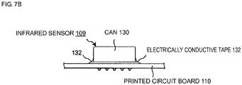
Fig. 7A is a perspective view illustrating the configuration of aninfrared sensor 109 of the related art disclosed inPatent Document 1.Fig. 7B is a side view of theinfrared sensor 109 illustrated inFig. 7A . In theinfrared sensor 109 illustrated inFig. 7A andFig. 7B , an electricallyconductive tape 132 is used for shielding theinfrared sensor 109, andFig. 7B illustrates aprinted circuit board 110 on which theinfrared sensor 109 is mounted. - In
Fig. 7A , aland 129 that is grounded to the ground of the printedcircuit board 110 and that has a rectangular frame shape is formed on a portion of the printedcircuit board 110 on which theinfrared sensor 109 is mounted. Acan 130 that is a metal case of theinfrared sensor 109 is disposed such that a lower end portion of thecan 130 is in contact with theland 129. Here, there is a slight gap between thecan 130 and theland 129, and in the related art, as illustrated inFig. 7A andFig. 7B , a shield structure is provided in which a contact portion where thecan 130 of theinfrared sensor 109 and theland 129 of the printedcircuit board 110 are in contact with each other is completely enclosed by the electricallyconductive tape 132 attached to the periphery of the contact portion. - As a result of the contact portion where the
can 130 of theinfrared sensor 109 and theland 129 of the printedcircuit board 110, which is grounded, are in contact with each other, being completely enclosed and covered by the electricallyconductive tape 132, even if there is a gap between thecan 130 and theland 129, the gap is electrically closed by the electricallyconductive tape 132, which is attached to the periphery of the contact portion so as to surround the contact portion, so that electrical airtightness can be ensured.Patent Document 1 discloses that, by providing the shield structure in which a gap between thecan 130 and theland 129 is electrically hermetically sealed by the electricallyconductive tape 132 as described above, even if radioactive noise is transmitted from the outside, the radioactive noise can be reliably prevented from flowing through the gap between thecan 130 and theland 129 onto a pin (a lead wire) of theinfrared sensor 109. - Patent Document 1: Japanese Unexamined Patent Application Publication No.
2002-122473 Fig. 5 ) - In the above-described case of the related art, the shield structure is fabricated by connecting the
can 130, which is the metal case of theinfrared sensor 109, to a ground GND and by using the electricallyconductive tape 132, such that the influence of an immunity signal from the outside is reduced. However, a ground pin of theinfrared sensor 109 and thecan 130, which is a shield case, are integrated with each other, and thus, theinfrared sensor 109 is not resistant to an immunity signal input from an external ground, so that there has been a problem in that a malfunction occurs in theinfrared sensor 109. - It is an object of the present invention to solve the above problem and to provide an infrared detection circuit and an infrared sensor which are resistant to an immunity signal input from an external ground and in which a malfunction does not occur.
- An infrared detection circuit according to a first aspect of the present invention detects infrared rays and outputs a detection signal to an external detection circuit.
- The infrared detection circuit includes an infrared sensor element and an impedance element that is connected between a ground of the infrared sensor element and a ground of the external detection circuit and that has at least one of resistivity and inductivity.
- In the infrared detection circuit, the impedance element blocks an immunity signal from outside.
- In the infrared detection circuit, the ground of the infrared sensor element is connected to the impedance element via a ground of an internal substrate of the infrared detection circuit.
- The infrared detection circuit further includes an impedance conversion circuit that performs impedance conversion on a detection signal from the infrared sensor element and outputs the detection signal.
- In the infrared detection circuit, the impedance conversion circuit includes a field-effect transistor, a voltage follower circuit using an operational amplifier, or an impedance conversion circuit of an integrated circuit.
- The infrared detection circuit further includes at least one of
- (1) a resistance element that is connected in parallel to the infrared sensor element,
- (2) an impedance element that is connected between a power supply terminal of the impedance conversion circuit and a power supply terminal of the infrared detection circuit, and
- (3) an impedance element that is connected between a signal output terminal of the impedance conversion circuit and a signal processing circuit of the external detection circuit.
- The infrared detection circuit further includes at least one of
- (1) a bypass capacitor that is connected between the power supply terminal of the infrared detection circuit and the ground of the infrared sensor element or the ground of the external detection circuit and
- (2) a bypass capacitor that is connected between the signal output terminal of the infrared detection circuit and the ground of the infrared sensor element or the ground of the external detection circuit.
- An infrared sensor according to a second aspect of the present invention detects infrared rays and outputs a detection signal to an external detection circuit.
- The infrared sensor includes an infrared sensor element and an impedance element that is connected between a ground of the infrared sensor element and a ground of the external detection circuit and that has at least one of resistivity and inductivity.
- In the infrared sensor, the impedance element blocks an immunity signal from outside.
- In the infrared sensor, the impedance element is disposed in a package of the infrared sensor.
- In the infrared sensor, the impedance element is disposed outside a package of the infrared sensor.
- In the infrared sensor, the ground of the infrared sensor element is connected to the impedance element via a ground of an internal substrate of the infrared sensor.
- The infrared sensor further includes an impedance conversion circuit that performs impedance conversion on a detection signal from the infrared sensor element and outputs the detection signal.
- In the infrared sensor, the impedance conversion circuit includes a field-effect transistor, a voltage follower circuit using an operational amplifier, or an impedance conversion circuit of an integrated circuit.
- The infrared sensor further includes at least one of
- (1) a resistance element that is connected in parallel to the infrared sensor element,
- (2) an impedance element that is connected between a power supply terminal of the impedance conversion circuit and a power supply terminal of the infrared sensor, and (3) an impedance element that is connected between a signal output terminal of the impedance conversion circuit and a signal processing circuit of the external detection circuit.
- The infrared sensor further includes at least one of
- (1) a bypass capacitor that is connected between the power supply terminal of the infrared sensor and the ground of the infrared sensor element or the ground of the external detection circuit and
- (2) a bypass capacitor that is connected between the signal output terminal of the infrared sensor and the ground of the infrared sensor element or the ground of the external detection circuit.
- In an infrared detection circuit and an infrared sensor according to the present invention, an immunity signal input from an external ground does not flow to the ground of the infrared detection circuit or the ground of the infrared sensor, and thus, a malfunction of the infrared sensor can be prevented.
-
-
Fig. 1 is a circuit diagram illustrating a configuration example of aninfrared detection circuit 10 according to a first embodiment. -
Fig. 2A is a circuit diagram illustrating a configuration example of aninfrared detection circuit 10A according to a second embodiment. -
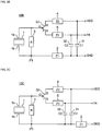
Fig. 2B is a circuit diagram illustrating a configuration example of aninfrared detection circuit 10B according to a first modification of the second embodiment. -
Fig. 2C is a circuit diagram illustrating a configuration example of aninfrared detection circuit 10C according to a second modification of the second embodiment. -
Fig. 3A is a circuit diagram illustrating a configuration example of aninfrared sensor 20 according to a third embodiment. -
Fig. 3B is a circuit diagram illustrating a configuration example of aninfrared sensor 20A according to a first modification of the third embodiment. -
Fig. 3C is a circuit diagram illustrating a configuration example of aninfrared sensor 20B according to a second modification of the third embodiment. -
Fig. 3D is a circuit diagram illustrating a configuration example of aninfrared sensor 20C according to a third modification of the third embodiment. -
Fig. 4A is a circuit diagram illustrating a configuration example of aninfrared sensor 20D according to a fourth embodiment. -
Fig. 4B is a circuit diagram illustrating a configuration example of aninfrared sensor 20E according to a first modification of the fourth embodiment and a configuration example of an external circuit according to the first modification of the fourth embodiment. -
Fig. 4C is a circuit diagram illustrating a configuration example of theinfrared sensor 20E according to a second modification of the fourth embodiment and a configuration example of an external circuit according to the second modification of the fourth embodiment. -
Fig. 4D is a circuit diagram illustrating a configuration example of theinfrared sensor 20E according to a third modification of the fourth embodiment and a configuration example of an external circuit according to the third modification of the fourth embodiment. -
Fig. 5 is a circuit diagram illustrating a configuration example of animpedance conversion circuit 7 according toModification 1. -
Fig. 6 is a circuit diagram illustrating a configuration example of anintegrated circuit 8 according toModification 2 that includes theimpedance conversion circuit 7. -
Fig. 7A is a perspective view illustrating a configuration of aninfrared sensor 109 of the related art. -
Fig. 7B is a side view of theinfrared sensor 109 illustrated inFig. 7A . - Embodiments of the present invention will be described below with reference to the drawings. Note that, in the following embodiments, similar components are denoted by the same reference signs.
-
Fig. 1 is a circuit diagram illustrating a configuration example of aninfrared detection circuit 10 according to a first embodiment. InFig. 1 , theinfrared detection circuit 10 includes apyroelectric element 1 that is an infrared sensor element, animpedance element 2 that is a passive element having at least one of a resistive impedance Z1 and an inductive impedance Z1, and a field-effect transistor (hereinafter referred to as FET) Q1 that is included in an impedance conversion circuit. In particular, a feature of theinfrared detection circuit 10 according to the first embodiment is that theinfrared detection circuit 10 includes theimpedance element 2. - In
Fig. 1 , thepyroelectric element 1, which is an infrared sensor element, includes asignal output terminal 1a and aground terminal 1b. Thesignal output terminal 1a is connected to the gate of the FET Q1, and a power supply voltage VDD is applied to the drain (a power supply terminal) of the FET Q1 from a power supply terminal of theinfrared detection circuit 10. The source of the FET Q1 is a signal output terminal for a detection signal and is connected to an external detection circuit of an external substrate (not illustrated). In contrast, theground terminal 1b is connected to a ground GND of the external substrate via a connection point P1 of an internal substrate of theinfrared detection circuit 10 and theimpedance element 2. Thepyroelectric element 1 and the FET Q1 are formed, for example, on the internal substrate of theinfrared detection circuit 10. The FET Q1 performs impedance conversion from a predetermined first impedance to a predetermined second impedance that is lower than the first impedance. An infrared detection signal that is output by thepyroelectric element 1 is output as an infrared detection voltage signal Vs to the external detection circuit via the FET Q1, which performs impedance conversion. - Here, the
impedance element 2 has any one of the following impedances Z1 and functions as a filter element that blocks a specified immunity signal that is radiated from the outside or that enters from the outside.


- Here, the symbol "ω" refers to angular frequency. Accordingly, as is clear from the formula (1) to the formula (3), the
impedance element 2 is formed of only a resistance element, only an inductance element, or a series circuit including a resistance element and an inductance element. - Here,
- (A) in the case where the
impedance element 2 is formed of only a resistance element, a resistance R1 is set such that the above-mentioned immunity signal from the outside can be prevented, by a resistive loss of the resistance element, from being input to theground terminal 1b of thepyroelectric element 1 from the ground GND of the external substrate. - (B) In the case where the
impedance element 2 is formed of only an inductance element, an inductance L1 is set such that the above-mentioned immunity signal from the outside can be prevented, by an inductive loss of the inductance element, from being input to theground terminal 1b of thepyroelectric element 1 from the ground GND of the external substrate. - (C) In the case where the
impedance element 2 is formed of a series circuit including a resistance element and an inductance element, the resistance R1 and the inductance L1 are set such that the above-mentioned immunity signal from the outside can be prevented, by the resistive loss of the resistance element and the inductive loss of the inductance element, from being input to theground terminal 1b of thepyroelectric element 1 from the ground GND of the external substrate. - Here, the above-mentioned immunity signal from the outside is, for example, an immunity signal having a frequency of about several tens of MHz to about several GHz, particularly, for example, a Wi-Fi signal that is used in a wireless LAN, a radio signal that is used in a cellular phone system, or the like. The
impedance element 2 is not a parasitic element and is provided as a passive element in order to prevent the immunity signal from being input to thepyroelectric element 1. - In the
infrared detection circuit 10, which is configured as described above, theimpedance element 2 is inserted between the connection point P1 of the internal substrate, which is connected to theground terminal 1b of thepyroelectric element 1, and a ground terminal of the external detection circuit, so that a radiation immunity signal radiated to theinfrared detection circuit 10 from the outside does not propagate to theground terminal 1b of thepyroelectric element 1 or to the connection point P1, which is connected to theground terminal 1b. Therefore, a malfunction of thepyroelectric element 1 in theinfrared detection circuit 10 can be prevented. - In the above-described embodiment, although the
impedance element 2 is connected between the connection point P1 of the internal substrate and the ground of the external substrate, the present invention is not limited to this configuration, and theground terminal 1b of thepyroelectric element 1 may be directly connected to the ground of the external substrate via theimpedance element 2. In other words, an end of theimpedance element 2 is directly or indirectly connected to theground terminal 1b of thepyroelectric element 1. This is common to the following embodiments and modifications. -
Fig. 2A is a circuit diagram illustrating a configuration example of aninfrared detection circuit 10A according to a second embodiment. As illustrated inFig. 2A , unlike theinfrared detection circuit 10 according to the first embodiment, which is illustrated inFig. 1 , theinfrared detection circuit 10A according to the second embodiment further includes the following elements. - (1) A
resistance element 3 that has a resistance R was connected to the two ends of thepyroelectric element 1 in parallel to thepyroelectric element 1. - (2) An
impedance element 4 that is a passive element having at least one of a resistive impedance Z2 and an inductive impedance Z2 was connected between the drain of the FET Q1 and the power supply terminal for the power supply voltage VDD (the power supply terminal of theinfrared detection circuit 10A). - (3) An
impedance element 5 that is a passive element having at least one of a resistive impedance Z3 and an inductive impedance Z3 was connected between the source of the FET Q1 and a signal output terminal that outputs the infrared detection voltage signal Vs. - Similar to the
infrared detection circuit 10 illustrated inFig. 1 , theinfrared detection circuit 10A, which is configured as described above, includes theimpedance element 2, and thus, a radiation immunity signal radiated to theinfrared detection circuit 10 from the outside does not flow to theground terminal 1b of thepyroelectric element 1 or to the connection point P1, which is connected to theground terminal 1b. Therefore, a malfunction of thepyroelectric element 1 in theinfrared detection circuit 10 can be prevented. - Note that, although the
resistance element 2 and theimpedance elements elements -
Fig. 2B is a circuit diagram illustrating a configuration example of aninfrared detection circuit 10B according to a first modification of the second embodiment. As illustrated inFig. 2B , unlike theinfrared detection circuit 10A according to the second embodiment, which is illustrated inFig. 2A , theinfrared detection circuit 10B according to the first modification of the second embodiment further includes the following elements inserted therein. - (1) A
bypass capacitor 31 having a capacitance C1 for causing the above-mentioned radiation immunity signal to bypass and flow to the ground GND was connected between the power supply terminal for the power supply voltage VDD and the ground GND. - (2) A
bypass capacitor 32 having a capacitance C2 for causing the above-mentioned radiation immunity signal to bypass and flow to the ground GND was connected between the signal output terminal, which outputs the infrared detection voltage signal Vs, and the ground GND. - According to the
infrared detection circuit 10B, which is configured as described above, in addition to the advantageous effect of theinfrared detection circuit 10A, the above-mentioned radiation immunity signal can be caused to bypass and flow to the ground GND by thebypass capacitors pyroelectric element 1 in theinfrared detection circuit 10 can be prevented. - Note that a configuration in which at least one of the
bypass capacitors -
Fig. 2C is a circuit diagram illustrating a configuration example of aninfrared detection circuit 10C according to a second modification of the second embodiment. As illustrated inFig. 2C , unlike theinfrared detection circuit 10A according to the second embodiment, which is illustrated inFig. 2A , theinfrared detection circuit 10B according to the second modification of the second embodiment further includes the following elements inserted therein. - (1) The
bypass capacitor 31 having the capacitance C1 for causing the above-mentioned radiation immunity signal to bypass and flow to the ground GND was connected between the power supply terminal for the power supply voltage VDD and the connection point P1. - (2) The
bypass capacitor 32 having the capacitance C2 for causing the above-mentioned radiation immunity signal to bypass and flow to the ground GND was connected between the signal output terminal, which outputs the infrared detection voltage signal Vs, and the connection point P1. - According to the
infrared detection circuit 10C, which is configured as described above, in addition to the advantageous effect of theinfrared detection circuit 10A, the above-mentioned radiation immunity signal can be caused to bypass and flow to the ground GND via theimpedance element 2 by thebypass capacitors pyroelectric element 1 in theinfrared detection circuit 10 can be prevented. -
Fig. 3A is a circuit diagram illustrating a configuration example of aninfrared sensor 20 according to a third embodiment. As illustrated inFig. 3A , unlike theinfrared detection circuit 10 according to the first embodiment, which is illustrated inFig. 1 , apackage 21 of theinfrared sensor 20 according to the third embodiment accommodates thepyroelectric element 1, the FET Q1, and theimpedance element 2 therein. - Similar to the
infrared detection circuit 10 illustrated inFig. 1 , thepackage 21 of theinfrared sensor 20, which is configured as described above, includes theimpedance element 2, and thus, a radiation immunity signal radiated to theinfrared detection circuit 10 from the outside does not flow to theground terminal 1b of thepyroelectric element 1 or to the connection point P1, which is connected to theground terminal 1b. Therefore, a malfunction of thepyroelectric element 1 in theinfrared sensor 20 can be prevented. - In the third embodiment, since the
pyroelectric element 1 is disposed in thepackage 21, a relatively strong shielding effect for thepyroelectric element 1 is provided, and as illustrated inFig. 3A , by preventing the influence of an immunity signal within theinfrared sensor 20, which includes thepyroelectric element 1, a stronger and more stable effect can be expected. -
Fig. 3B is a circuit diagram illustrating a configuration example of aninfrared sensor 20A according to a first modification of the third embodiment. Unlike theinfrared sensor 20 according to the third embodiment, which is illustrated inFig. 3A , and similar to theinfrared detection circuit 10A according to the second embodiment, which is illustrated inFig. 2A , theinfrared sensor 20A according to the first modification of the third embodiment further includes theresistance element 3 and theimpedance elements package 21B of theinfrared sensor 20A as illustrated inFig. 3B . Theinfrared sensor 20A, which is configured as described above, has an advantageous effect similar to that of theinfrared detection circuit 10A according to the second embodiment, which is illustrated inFig. 2A . -
Fig. 3C is a circuit diagram illustrating a configuration example of aninfrared sensor 20B according to a second modification of the third embodiment. Unlike theinfrared sensor 20A according to the first modification of the third embodiment, which is illustrated inFig. 3B , and similar to theinfrared detection circuit 10B according to the first modification of the second embodiment, which is illustrated inFig. 2B , theinfrared sensor 20B according to the second modification of the third embodiment further includes thebypass capacitors package 21C of theinfrared sensor 20A as illustrated inFig. 3C . Theinfrared sensor 20B, which is configured as described above, has an advantageous effect similar to that of theinfrared detection circuit 10B according to the first modification of the second embodiment, which is illustrated inFig. 2B . -
Fig. 3D is a circuit diagram illustrating a configuration example of aninfrared sensor 20C according to a third modification of the third embodiment. Compared with theinfrared sensor 20A according to the second modification of the third embodiment, which is illustrated inFig. 3C , and similar to theinfrared detection circuit 10C according to the second modification of the second embodiment, which is illustrated inFig. 2C , theinfrared sensor 20C according to the third modification of the third embodiment further includes thebypass capacitors package 21C of theinfrared sensor 20A as illustrated inFig. 3D . Theinfrared sensor 20C, which is configured as described above, has an advantageous effect similar to that of theinfrared detection circuit 10B according to the second modification of the second embodiment, which is illustrated inFig. 2C . -
Fig. 4A is a circuit diagram illustrating a configuration example of aninfrared sensor 20D according to a fourth embodiment. As illustrated inFig. 4A , unlike theinfrared detection circuit 10 according to the first embodiment, which is illustrated inFig. 1 , apackage 21A of theinfrared sensor 20D according the third embodiment accommodates thepyroelectric element 1 and the FET Q1 therein, and theimpedance element 2 is not accommodated in thepackage 21A and is connected between thepackage 21A of theinfrared sensor 20D and an external detection circuit. - Similar to the
infrared detection circuit 10 illustrated inFig. 1 , thepackage 21A of theinfrared sensor 20D, which is configured as described above, includes theimpedance element 2, and thus, a radiation immunity signal radiated to theinfrared detection circuit 10 from the outside does not flow to theground terminal 1b of thepyroelectric element 1 or to the connection point P1, which is connected to theground terminal 1b. Therefore, a malfunction of thepyroelectric element 1 in theinfrared sensor 20D can be prevented. - Similar to the third embodiment, in the fourth embodiment, since the
pyroelectric element 1 is disposed in thepackage 21A, a relatively strong shielding effect for thepyroelectric element 1 is provided, and as illustrated inFig. 4A , by preventing the influence of an immunity signal outside theinfrared sensor 20D, which includes thepyroelectric element 1, a stronger and more stable effect can be expected. -
Fig. 4B is a circuit diagram illustrating a configuration example of aninfrared sensor 20E according to a first modification of the fourth embodiment and a configuration example of an external circuit according to the first modification of the fourth embodiment. Unlike theinfrared sensor 20D and the external circuit according to the third embodiment, which are illustrated inFig. 4A , and similar to theinfrared detection circuit 10A according to the second embodiment, which is illustrated inFig. 2A , theinfrared sensor 20E according to the first modification of the fourth embodiment includes theresistance element 3 disposed in apackage 21E of theinfrared sensor 20E, and theimpedance elements package 21E of theinfrared sensor 20E, as illustrated inFig. 4B . Theinfrared sensor 20E and the external circuit, which are configured as described above, have an advantageous effect similar to that of theinfrared detection circuit 10A according to the second embodiment, which is illustrated inFig. 2A . -
Fig. 4C is a circuit diagram illustrating a configuration example of theinfrared sensor 20E according to a second modification of the fourth embodiment and a configuration example of an external circuit according to the second modification of the fourth embodiment. Regarding theinfrared sensor 20E and the external circuit according to the second modification of the fourth embodiment, unlike theinfrared sensor 20E and the external circuit according to the first modification of the fourth embodiment, which are illustrated inFig. 4B , and similar to theinfrared detection circuit 10B according to the first modification of the second embodiment, which is illustrated inFig. 2B , thebypass capacitors package 21E of theinfrared sensor 20E as illustrated inFig. 4C . Theinfrared sensor 20E and the external circuit, which are configured as described above, have an advantageous effect similar to that of theinfrared detection circuit 10B according to the first modification of the second embodiment, which is illustrated inFig. 2B . -
Fig. 4D is a circuit diagram illustrating a configuration example of theinfrared sensor 20E according to a third modification of the fourth embodiment and a configuration example of an external circuit according to the third modification of the fourth embodiment. Regarding theinfrared sensor 20E and the external circuit according to the third modification of the fourth embodiment, Compared with theinfrared sensor 20E and the external circuit according to the second modification of the fourth embodiment, which are illustrated inFig. 4C , and similar to theinfrared detection circuit 10C according to the second modification of the second embodiment, which is illustrated inFig. 2C , thebypass capacitors package 21E of theinfrared sensor 20E as illustrated inFig. 4D . Theinfrared sensor 20E and the external circuit, which are configured as described above, have an advantageous effect similar to that of theinfrared detection circuit 10B according to the second modification of the second embodiment, which is illustrated inFig. 2C . -
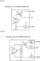
Fig. 5 is a circuit diagram illustrating a configuration example of animpedance conversion circuit 7 according toModification 1. In the first to fourth embodiments and their modifications, the FET Q1 is provided as an impedance conversion circuit. However, the present invention is not limited to this configuration, and as inModification 1 illustrated inFig. 5 , a voltage follower circuit using anoperational amplifier 6 may be formed as theimpedance conversion circuit 7. InFig. 5 , theoperational amplifier 6 is, for example, a differential amplifier. A non-inverting input terminal of theoperational amplifier 6 is connected to thesignal output terminal 1a of thepyroelectric element 1, and an inverting input terminal of theoperational amplifier 6 is connected to an output terminal of theoperational amplifier 6. The power supply terminal for the power supply voltage VDD (the power supply terminal of one of theinfrared detection circuits infrared sensors 20 to 20E) and the ground GND are connected to theoperational amplifier 6. - Similar to the FER Q1, the
impedance conversion circuit 7 according toModification 1, which is configured as described above, performs impedance conversion from a predetermined first impedance to a predetermined second impedance that is lower than the first impedance. -
Fig. 6 is a circuit diagram illustrating a configuration example of anintegrated circuit 8 according toModification 2 that includes theimpedance conversion circuit 7. As illustrated inFig. 6 , for example, theimpedance conversion circuit 7 illustrated inFig. 5 may be formed of theintegrated circuit 8. Note that theimpedance conversion circuit 7 may be the FET Q1 illustrated inFig. 1 to Fig. 4D . - As described in detail above, in the infrared detection circuit and the infrared sensor according to the present invention, an immunity signal applied from the outside does not flow to the ground of the infrared detection circuit or the ground of the infrared sensor, and thus, a malfunction can be prevented.
- Note that an example of an immunity signal that is prevented from entering by the
impedance element 2 according to the present embodiment and the like is an immunity signal having a frequency of about several tens of MHz to about several GHz, particularly, for example, a Wi-Fi signal that is used in a wireless LAN, a radio signal that is used in a cellular phone system, or the like. -
- 1
- pyroelectric element
- 1a
- signal output terminal
- 1b
- ground terminal
- 2, 4, 5
- impedance element
- 3
- resistance element
- 6
- operational amplifier
- 7
- impedance conversion circuit
- 8
- integrated circuit
- 10, 10A, 10B, 10C
- infrared detection circuit
- 20, 20A, 20B, 20C, 20D, 20E
- infrared sensor
- 21, 21A, 21B, 21C, 21D, 21E
- package
- 31, 32
- bypass capacitor
- P1
- ground terminal of internal substrate
- Q1
- field-effect transistor (FET)
Claims (16)
- An infrared detection circuit that detects infrared rays and outputs a detection signal to an external detection circuit, the infrared detection circuit comprising:an infrared sensor element; andan impedance element that is connected between a ground of the infrared sensor element and a ground of the external detection circuit and that has at least one of resistivity and inductivity.
- The infrared detection circuit according to Claim 1,
wherein the impedance element blocks an immunity signal from outside. - The infrared detection circuit according to Claim 1 or 2,
wherein the ground of the infrared sensor element is connected to the impedance element via a ground of an internal substrate of the infrared detection circuit. - The infrared detection circuit according to any one of Claims 1 to 3, further comprising:
an impedance conversion circuit that performs impedance conversion on a detection signal from the infrared sensor element and outputs the detection signal. - The infrared detection circuit according to Claim 4,
wherein the impedance conversion circuit includes a field-effect transistor, a voltage follower circuit using an operational amplifier, or an impedance conversion circuit of an integrated circuit. - The infrared detection circuit according to Claim 4 or 5, further comprising at least one of:(1) a resistance element that is connected in parallel to the infrared sensor element;(2) an impedance element that is connected between a power supply terminal of the impedance conversion circuit and a power supply terminal of the infrared detection circuit; and(3) an impedance element that is connected between a signal output terminal of the impedance conversion circuit and a signal processing circuit of the external detection circuit.
- The infrared detection circuit according to Claim 6, further comprising at least one of:(1) a bypass capacitor that is connected between the power supply terminal of the infrared detection circuit and the ground of the infrared sensor element or the ground of the external detection circuit; and(2) a bypass capacitor that is connected between the signal output terminal of the infrared detection circuit and the ground of the infrared sensor element or the ground of the external detection circuit.
- An infrared sensor that detects infrared rays and outputs a detection signal to an external detection circuit, the infrared sensor comprising:an infrared sensor element; andan impedance element that is connected between a ground of the infrared sensor element and a ground of the external detection circuit and that has at least one of resistivity and inductivity.
- The infrared sensor according to Claim 8,
wherein the impedance element blocks an immunity signal from outside. - The infrared sensor according to Claim 8 or 9,
wherein the impedance element is disposed in a package of the infrared sensor. - The infrared sensor according to Claim 8 or 9,
wherein the impedance element is disposed outside a package of the infrared sensor. - The infrared sensor according to any one of Claims 8 to 11,
wherein the ground of the infrared sensor element is connected to the impedance element via a ground of an internal substrate of the infrared sensor. - The infrared sensor according to any one of Claims 8 to 12, further comprising:
an impedance conversion circuit that performs impedance conversion on a detection signal from the infrared sensor element and outputs the detection signal. - The infrared sensor according to Claim 13,
wherein the impedance conversion circuit includes a field-effect transistor, a voltage follower circuit using an operational amplifier, or an impedance conversion circuit of an integrated circuit. - The infrared sensor according to Claim 13 or 14, further comprising at least one of:(1) a resistance element that is connected in parallel to the infrared sensor element;(2) an impedance element that is connected between a power supply terminal of the impedance conversion circuit and a power supply terminal of the infrared sensor; and(3) an impedance element that is connected between a signal output terminal of the impedance conversion circuit and a signal processing circuit of the external detection circuit.
- The infrared sensor according to Claim 15, further comprising at least one of:(1) a bypass capacitor that is connected between the power supply terminal of the infrared sensor and the ground of the infrared sensor element or the ground of the external detection circuit and(2) a bypass capacitor that is connected between the signal output terminal of the infrared sensor and the ground of the infrared sensor element or the ground of the external detection circuit.
Applications Claiming Priority (2)
| Application Number | Priority Date | Filing Date | Title |
|---|---|---|---|
| JP2016221853 | 2016-11-14 | ||
| PCT/JP2017/040134 WO2018088401A1 (en) | 2016-11-14 | 2017-11-07 | Infrared detecting circuit and infrared sensor |
Publications (2)
| Publication Number | Publication Date |
|---|---|
| EP3540391A1 true EP3540391A1 (en) | 2019-09-18 |
| EP3540391A4 EP3540391A4 (en) | 2020-06-03 |
Family
ID=62110746
Family Applications (1)
| Application Number | Title | Priority Date | Filing Date |
|---|---|---|---|
| EP17870099.3A Withdrawn EP3540391A4 (en) | 2016-11-14 | 2017-11-07 | INFRARED DETECTION CIRCUIT AND INFRARED SENSOR |
Country Status (5)
| Country | Link |
|---|---|
| US (1) | US10809130B2 (en) |
| EP (1) | EP3540391A4 (en) |
| JP (1) | JP6662469B2 (en) |
| CN (1) | CN109952494A (en) |
| WO (1) | WO2018088401A1 (en) |
Families Citing this family (3)
| Publication number | Priority date | Publication date | Assignee | Title |
|---|---|---|---|---|
| CN111402554A (en) * | 2020-03-23 | 2020-07-10 | 合肥星空物联信息科技有限公司 | Device capable of correcting sitting posture and preventing myopia |
| GB202008691D0 (en) * | 2020-06-09 | 2020-07-22 | Ams Int Ag | Ambient light sensing |
| US12015098B2 (en) | 2020-12-25 | 2024-06-18 | Asahi Kasei Microdevices Corporation | Photodetection apparatus |
Family Cites Families (29)
| Publication number | Priority date | Publication date | Assignee | Title |
|---|---|---|---|---|
| JPH0530105Y2 (en) * | 1987-05-29 | 1993-08-02 | ||
| JPS6447920A (en) | 1987-08-19 | 1989-02-22 | Matsushita Electric Industrial Co Ltd | Infrared-ray detector |
| DE8714248U1 (en) * | 1987-10-26 | 1989-02-23 | Heimann Optoelectronics Gmbh, 65199 Wiesbaden | Infrared detector |
| JPH02254395A (en) * | 1989-03-29 | 1990-10-15 | Nippon Arefu:Kk | Pyroelectric type human body detector |
| JPH03176621A (en) | 1989-12-06 | 1991-07-31 | Nippon Ceramic Co Ltd | Pyroelectric type infrared-ray detector |
| JPH04118637U (en) | 1991-04-09 | 1992-10-23 | 能美防災株式会社 | flame detector |
| JP2753920B2 (en) | 1992-02-19 | 1998-05-20 | 能美防災株式会社 | Pyroelectric element |
| JPH05340807A (en) | 1992-06-12 | 1993-12-24 | Murata Mfg Co Ltd | Infrared detector |
| JP2607440Y2 (en) | 1992-10-07 | 2001-09-04 | 北陸電気工業株式会社 | Pyroelectric sensor |
| JPH085552A (en) * | 1994-06-14 | 1996-01-12 | Tokuyama Corp | Non-dispersive infrared gas detector |
| JP3278300B2 (en) * | 1994-09-07 | 2002-04-30 | 株式会社リコー | Image forming device |
| KR0131569Y1 (en) | 1995-12-30 | 1998-12-01 | 김광호 | Pyroelectric infrared sensor |
| DE19619459C2 (en) * | 1996-05-14 | 2000-06-08 | Heimann Optoelectronics Gmbh | Circuit for the detection of electromagnetic radiation |
| JPH1183623A (en) | 1997-09-08 | 1999-03-26 | Daishinku Co | Pyroelectric infrared detector |
| JP3391236B2 (en) * | 1997-10-07 | 2003-03-31 | 株式会社村田製作所 | Infrared sensor |
| US6395575B1 (en) | 1998-05-22 | 2002-05-28 | Matsushita Electric Industrial Co., Ltd. | Method of manufacturing sensor and resistor element |
| JP2002122473A (en) | 2000-10-13 | 2002-04-26 | Hochiki Corp | Infrared detector |
| JP3591445B2 (en) | 2000-10-16 | 2004-11-17 | 三菱電機株式会社 | Infrared camera |
| CN2785051Y (en) * | 2005-01-24 | 2006-05-31 | 郑国恩 | Anti-interference pyroelectric infrared sensor |
| JP5470545B2 (en) * | 2008-12-22 | 2014-04-16 | 竹中エンジニアリング株式会社 | Infrared sensor photoelectric conversion circuit |
| JP5325688B2 (en) * | 2009-07-22 | 2013-10-23 | 株式会社日立製作所 | Signal amplification circuit, optical receiver circuit, optical module, and data exchange system |
| JP2011205210A (en) * | 2010-03-24 | 2011-10-13 | Okaya Electric Industries Co Ltd | Noise filter |
| US20130032718A1 (en) * | 2011-08-03 | 2013-02-07 | Robert Bosch Gmbh | Rf immunity improved pyro sensor |
| US20140042320A1 (en) * | 2012-08-08 | 2014-02-13 | Excelitas Technologies Singapore Pte. Ltd. | Emi filtering detector and method for same |
| JP6202245B2 (en) | 2013-03-22 | 2017-09-27 | セイコーエプソン株式会社 | Infrared sensor and thermoelectric conversion element |
| JP2014185982A (en) | 2013-03-25 | 2014-10-02 | Seiko Epson Corp | Infrared sensor and thermal detector element |
| JP6409959B2 (en) * | 2015-04-06 | 2018-10-24 | 株式会社村田製作所 | Pyroelectric infrared detector |
| CN205504912U (en) * | 2016-01-27 | 2016-08-24 | 北京云端文化传媒股份有限公司 | Automatic indoor dimming system |
| CN205414330U (en) * | 2016-03-07 | 2016-08-03 | 北京创通建设集团有限公司 | Real formula molding machine of little jolt squeeze |
-
2017
- 2017-11-07 EP EP17870099.3A patent/EP3540391A4/en not_active Withdrawn
- 2017-11-07 JP JP2018550213A patent/JP6662469B2/en not_active Expired - Fee Related
- 2017-11-07 WO PCT/JP2017/040134 patent/WO2018088401A1/en not_active Ceased
- 2017-11-07 CN CN201780070389.9A patent/CN109952494A/en active Pending
-
2019
- 2019-04-15 US US16/383,872 patent/US10809130B2/en not_active Expired - Fee Related
Also Published As
| Publication number | Publication date |
|---|---|
| CN109952494A (en) | 2019-06-28 |
| JP6662469B2 (en) | 2020-03-11 |
| US20190242754A1 (en) | 2019-08-08 |
| EP3540391A4 (en) | 2020-06-03 |
| JPWO2018088401A1 (en) | 2019-06-24 |
| WO2018088401A1 (en) | 2018-05-17 |
| US10809130B2 (en) | 2020-10-20 |
Similar Documents
| Publication | Publication Date | Title |
|---|---|---|
| EP2910918B1 (en) | Pressure sensor and sensor unit provided with the same | |
| US9276400B2 (en) | Protection circuit | |
| US10809130B2 (en) | Infrared detection circuit and infrared sensor | |
| CN105210235B (en) | Electronic equipment | |
| CN111587538B (en) | switch module | |
| US6307252B1 (en) | On-chip shielding of signals | |
| JPS60125530A (en) | Infrared ray sensor | |
| CN111492591B (en) | IC chip | |
| US20120170773A1 (en) | Amplifier with high-frequency noise removing function, microphone module, and sensor module | |
| KR101938931B1 (en) | Reducing the effect of parasitic mismatch at amplifier inputs | |
| CN114502909B (en) | Displacement sensor and displacement sensor system | |
| KR920001113B1 (en) | Pyroelectric infrared sensor | |
| EP0145457B1 (en) | An infrared sensor | |
| JP6843312B1 (en) | Circuit boards and electronic devices | |
| US12130319B2 (en) | Electrostatic charge sensor with high impedance contact pads | |
| CN101227787A (en) | Anti-static electronic equipment and its anti-static method | |
| US8619435B2 (en) | Electromagnetic interference (EMI) diverter | |
| CN109818684B (en) | Signal processing system and terminal device | |
| CN109634148A (en) | Electronic equipment with radio-frequency enabled | |
| CN214591330U (en) | A high-precision positioning antenna | |
| Elena et al. | Methods of reducing capacitive coupling on the surface of a PCB | |
| US20120051003A1 (en) | Printed circuit board | |
| JPH0297107A (en) | Noise generation preventing circuit for ic element | |
| JP2018078175A (en) | Implementation structure of common mode noise filter |
Legal Events
| Date | Code | Title | Description |
|---|---|---|---|
| STAA | Information on the status of an ep patent application or granted ep patent |
Free format text: STATUS: THE INTERNATIONAL PUBLICATION HAS BEEN MADE |
|
| PUAI | Public reference made under article 153(3) epc to a published international application that has entered the european phase |
Free format text: ORIGINAL CODE: 0009012 |
|
| STAA | Information on the status of an ep patent application or granted ep patent |
Free format text: STATUS: REQUEST FOR EXAMINATION WAS MADE |
|
| 17P | Request for examination filed |
Effective date: 20190329 |
|
| AK | Designated contracting states |
Kind code of ref document: A1 Designated state(s): AL AT BE BG CH CY CZ DE DK EE ES FI FR GB GR HR HU IE IS IT LI LT LU LV MC MK MT NL NO PL PT RO RS SE SI SK SM TR |
|
| AX | Request for extension of the european patent |
Extension state: BA ME |
|
| DAV | Request for validation of the european patent (deleted) | ||
| DAX | Request for extension of the european patent (deleted) | ||
| A4 | Supplementary search report drawn up and despatched |
Effective date: 20200507 |
|
| RIC1 | Information provided on ipc code assigned before grant |
Ipc: G01J 5/00 20060101AFI20200429BHEP Ipc: G08B 13/19 20060101ALI20200429BHEP |
|
| STAA | Information on the status of an ep patent application or granted ep patent |
Free format text: STATUS: THE APPLICATION HAS BEEN WITHDRAWN |
|
| 18W | Application withdrawn |
Effective date: 20210608 |