EP3538883B1 - Sensitive feldeffektvorrichtung - Google Patents
Sensitive feldeffektvorrichtung Download PDFInfo
- Publication number
- EP3538883B1 EP3538883B1 EP17719015.4A EP17719015A EP3538883B1 EP 3538883 B1 EP3538883 B1 EP 3538883B1 EP 17719015 A EP17719015 A EP 17719015A EP 3538883 B1 EP3538883 B1 EP 3538883B1
- Authority
- EP
- European Patent Office
- Prior art keywords
- field effect
- oxide
- sensor according
- rfid
- dielectric layer
- Prior art date
- Legal status (The legal status is an assumption and is not a legal conclusion. Google has not performed a legal analysis and makes no representation as to the accuracy of the status listed.)
- Active
Links
Images




Classifications
-
- G—PHYSICS
- G01—MEASURING; TESTING
- G01N—INVESTIGATING OR ANALYSING MATERIALS BY DETERMINING THEIR CHEMICAL OR PHYSICAL PROPERTIES
- G01N27/00—Investigating or analysing materials by the use of electric, electrochemical, or magnetic means
- G01N27/26—Investigating or analysing materials by the use of electric, electrochemical, or magnetic means by investigating electrochemical variables; by using electrolysis or electrophoresis
- G01N27/403—Cells and electrode assemblies
- G01N27/414—Ion-sensitive or chemical field-effect transistors, i.e. ISFETS or CHEMFETS
-
- G—PHYSICS
- G01—MEASURING; TESTING
- G01T—MEASUREMENT OF NUCLEAR OR X-RADIATION
- G01T1/00—Measuring X-radiation, gamma radiation, corpuscular radiation, or cosmic radiation
- G01T1/16—Measuring radiation intensity
- G01T1/24—Measuring radiation intensity with semiconductor detectors
-
- H—ELECTRICITY
- H10—SEMICONDUCTOR DEVICES; ELECTRIC SOLID-STATE DEVICES NOT OTHERWISE PROVIDED FOR
- H10D—INORGANIC ELECTRIC SEMICONDUCTOR DEVICES
- H10D30/00—Field-effect transistors [FET]
- H10D30/60—Insulated-gate field-effect transistors [IGFET]
- H10D30/67—Thin-film transistors [TFT]
- H10D30/674—Thin-film transistors [TFT] characterised by the active materials
- H10D30/6755—Oxide semiconductors, e.g. zinc oxide, copper aluminium oxide or cadmium stannate
- H10D30/6756—Amorphous oxide semiconductors
-
- H—ELECTRICITY
- H10—SEMICONDUCTOR DEVICES; ELECTRIC SOLID-STATE DEVICES NOT OTHERWISE PROVIDED FOR
- H10D—INORGANIC ELECTRIC SEMICONDUCTOR DEVICES
- H10D30/00—Field-effect transistors [FET]
- H10D30/60—Insulated-gate field-effect transistors [IGFET]
- H10D30/67—Thin-film transistors [TFT]
- H10D30/6758—Thin-film transistors [TFT] characterised by the insulating substrates
-
- G—PHYSICS
- G01—MEASURING; TESTING
- G01T—MEASUREMENT OF NUCLEAR OR X-RADIATION
- G01T1/00—Measuring X-radiation, gamma radiation, corpuscular radiation, or cosmic radiation
- G01T1/36—Measuring spectral distribution of X-rays or of nuclear radiation spectrometry
- G01T1/366—Measuring spectral distribution of X-rays or of nuclear radiation spectrometry with semi-conductor detectors
Definitions
- the present invention relates to a sensitive field effect device.
- the invention concerns a field effect transistor, designed to feature a low leakage current as well as a high bandwidth, so as to be highly sensitive, if compared with analogous sensors according to the prior art.
- the field effect transistor is also particularly indicated for detecting circuits and designed to detect several kind of physical quantities, such as temperature, mechanical stresses, light, chemicals, ionizing radiation, such as X-rays and the like, and also suitable to be arranged in flexible substrates arrays or matrix.
- a RFID chip probes impedance of the connected sensor at high bandwidth (of the order of 100 kHz).
- An impedance Z greater of 20 M ⁇ results in the state 0, instead a value of said impedance Z below 2 M ⁇ results in the state 1.
- a technical problem currently felt in the field is that of creating sensors that (i) operate at the high bandwidth of RFID, while consuming little power, (ii) show an order of magnitude variation in impedance response in a given range triggered by the sensing event, (iii) maintain the impedance variation also after the occurrence of the sensing event and (iv) are compliant to low cost-mass production technology.
- RFID chips are based on CMOS technology, which however features some limits to accomplish the above objectives, due to the current leakage phenomena, which increase considerably the power consumption of the single field effect transistor.
- a wearable detector which combines low-voltage and low-power operation with high sensitivity, low-weight and flexible mechanical properties.
- thermoluminescent phosphate glasses or gafchromic film can actually achieve a high sensitivity.
- these dosimeters do not allow real-time detection of the radiation, but require readout in a dedicated instrument after exposure by optical techniques.
- a second type of dosimeters employs silicon complementary metal oxide semiconductor electronics and provides direct electronic readout, thus providing real-time data about radiation exposure.
- Drawbacks of this technical approach are reduced sensitivities due to the absorption of only a fraction of exposed ionizing particles, mechanical rigidity of the sensors and the impossibility to process devices on large areas of flexible substrates.
- these devices are not mechanically flexible, and therefore of limited use for wearable dosimeters.
- the relevant prior art comprises the scientific paper by Tobias Cramer et al. "Radiation - Tolerant Flexible Large Area Electronics based on Oxide Semiconductors", the scientific paper by Zhao Chumin et al. "Amorphous In-Ga-Zn-O thin-film transistor active pixel sensor x-ray imager for digital", the patent application US 2015/330941 A1 , the scientific paper by Lujan R. et al. “Flexible X-Ray detector Array Fabricated With Oxide Thin-Film Transistors”, and the scientific paper by H. Tsai et al. "Comprehensive Nuclear Material Surveillance with a Radiation Detector-Equipped ARG-US RFID System Introduction.
- FISFET flexible ionization sensitive field effect transistor
- the present invention provides a detecting sensor in accordance with claim 1.
- Advantageus features are provided in the dependent claims.
- a method for manufacturing a field effect device which is not part of the present invention and comprises the following steps: (A) depositing said gate electrode on said flexible substrate and carrying out a photolithography and etching process or lift-off on said gate electrode; (B) depositing said dielectric layer and carrying out a photolithography and etching process or lift-off on said dielectric layer; (C) depositing said semiconductor channel and carrying out a photolithography and etching process or lift-off on said semiconductor channel; (D) carrying out a photolithography process on said semiconductor channel and depositing said source electrode and said drain electrode; and (E) patterning said source electrode and said drain electrode by lift-off.
- Said step (B) could be carried out by RF-sputtering, performed in parallel from two separate targets containing said insulating material of said insulating layer and said material of said main layer of said dielectric, and/or via solution-based processes containing said material of said insulating layer and said material of said main layer of said dielectric, so as to create the multilayer structure of said dielectric layer, by alternating depositions of an insulating layer only, such as silicon-dioxide (SiO 2 ) and/or aluminum-oxide (Al 2 O 3 ), and co-depositions of an insulating material, such as silicon-dioxide (SiO 2 ) and/or aluminum-oxide (Al 2 O 3 ), and said material of said main layer of said dielectric.
- an insulating layer only such as silicon-dioxide (SiO 2 ) and/or aluminum-oxide (Al 2 O 3 )
- co-depositions of an insulating material such as silicon-dioxide (
- FIG 1 a first embodiment of a field effect device 100 according to the invention is shown, wherein details of the device architecture are also specified, for detecting electromagnetic radiations and particularly ionizing radiations, such as X-rays and the like.
- the device 100 mainly comprises source, drain and gate electrodes, indicated with reference numbers 120, 130 and 140 respectively, a semiconductor channel layer 110, arranged on a dielectric layer 150, and a substrate 160.
- Said source electrode 120, said drain electrode 130 and said gate electrode 140 are made of a conductive material, such as molybdenum (Mo), copper (Cu), aluminum (Al), gold (Au) or silver (Ag), or even conducting oxides, such as Gallium Zinc Oxide, Indium Zinc Oxide.
- Mo molybdenum
- Cu copper
- Al aluminum
- Au gold
- Ag silver
- conducting oxides such as Gallium Zinc Oxide, Indium Zinc Oxide.
- Said dielectric layer 150 has a thickness greater than 150 nm, so as to prevent the tunneling effects and the relevant leakage currents. This allows also reducing the overall leakage current effects possibly due to other phenomena.
- the semiconductor channel layer 110 is arranged between, and in electric contact with said source electrode 120 and said drain electrode 130.
- Said semiconductor channel layer 110 is made of a high mobility amorphous oxide.
- said semiconductor channel layer 110 can be made of Indium Gallium Zinc Oxide (IGZO), Indium Hafnium Zinc Oxide (IHZO), Zinc Tin Oxide (ZTO) or Gallium Zinc Tin Oxide (GZTO).
- IGZO Indium Gallium Zinc Oxide
- IHZO Indium Hafnium Zinc Oxide
- ZTO Zinc Tin Oxide
- GZTO Gallium Zinc Tin Oxide
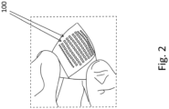
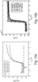
- the high mobility amorphous oxides used for said semiconductor channel layer 110 are fabricated by photolithography. They feature high bandwidth, low parasitic capacitance and minimal gate current, as it can be appreciated from figure 2 and are thus compliant to low-voltage operation, particularly with RFID circuits.
- Said field effect device 100 comprises also sensor means, so that, upon sensing an event to be detected, the impedance, commonly referred to with the letter Z, of the semiconductor channel layer 110 is varied by over an order of magnitude, thus allowing the connection of a RFID transmitter, as better explained below.
- the semiconductor channel layer 110 is exposed to the radiation to be detected.
- the sensing means provided in the field effect device 100 comprises multilayer dielectric oxide structure dielectric layer 150, comprising a main layer, combined with one or more further layers with lower atomic number atoms.
- Said main layer is a high-Z layer, this meaning that the atomic number is higher than 36.
- said main layer is made of at least one of the following materials:
- Said one or more further layers with lower atomic number atoms is an insulating layer that can be for example SiO 2 or Al 2 O 3 .
- the bottom layer of the multicomponent dielectric is said insulating layer with lower atomic number atoms, followed by the main layer. This structure is then repeated two to ten times, followed by a top layer of the said insulating layer with lower atomic number atoms.
- the dielectric layer 150 is deposited on said flexible substrates 160 such as Polyethylene Naphthalate, to achieve flexible sensitive field effect device 100. More specifically, in figure 2 , arrays patterned on polymeric/plastic substrates are shown, comprising a plurality of ionization sensitive field effect devices 100.
- the gate electrode 140 is arranged between said flexible substrates 160 and said dielectric layer 150.
- the operation of the device 100, based on the accumulation of ionization charges in the multilayer dielectric oxide structure 150 due to X-ray radiation as described above is as follows.
- the formation of ionization charge is initiated by the absorption of a high-energy photon or photoelectron 200 (see figure 3a ), giving the generation of an electron hole pair 310 in the dielectric layer 150.
- the electrons 311 are collected in a fast process, namely faster than respective holes collection process, at the gate electrode 140.
- the remaining hole charges 312 move, as said, slowly in a thermally activated hopping process to the interface with the semiconductor channel 110 (see figure 3c ).
- the transfer characteristics show a shift of 0,326 V to more negative gate potentials, after X-ray exposure (reference to figure 3a state).
- No other transistor parameter, such as sub-threshold slope or mobility is influenced by the exposure.
- the shift is a consequence of the positive carriers accumulation at the interfaces between the dielectric layer 150 and the semiconductor channel 110 (see figure 3c ).
- Positive carriers accumulation influences the voltage between said source electrodes 120 and said gate electrode 130 at fixed current flux.
- Sensitivity of the device 100 to ionization depends crucially on the composition and thickness of the high-Z dielectric multilayer 150.
- the ionization sensitive field effect device 100 allows to perform quantitative dosimetry by monitoring variations in threshold, as it offers a linear dependency between exposure dose and threshold shift for total doses remaining below 100 mGy.
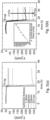
- FIG. 5b shows the variation of threshold voltage caused by exposure to X-ray 200 of varying dose-rates for a period of 1 sec.
- the inset shows the resulting shift in threshold voltage as a function of dose.
- the linear fit results in a sensitivity of 5,5 mV/mGy.
- the device 100 operates as an integrating dosimeter and maintains the threshold voltage after the X-ray exposure event.
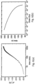
- Figures 6a and 6b displays a recovery measurement, in which the threshold voltage was monitored for 22 hours after an exposure to a dose of 21 Gy.
- the curve follows a stretched exponential with a characteristic time-scale of a few hours.
- the maximum readout time interval is defined here as the time after an X-ray exposure event in which the drift in threshold voltage remains below 10%.
- the maximum readout time exceeds 300 sec. This long retention time makes even the sequential readout of a large detector array feasible.
- the manufacturing of an ionization sensitive field effect device 100 comprises the following main steps.
- the gate electrode 140 is deposited on the flexible substrates 160 using materials processing via physics routes such as sputtering or chemical routes, such as solution based processes, such as screen printing, sol gel, among others. Patterning of gate electrodes 140 is performed with photolithography and etching processes or lift-off.
- the dielectric layer 150 can be deposited using different techniques such as RF-sputtering, from two separate targets containing SiO 2 and Ta 2 O 5 or via solution-based processes, containing the elements above mentioned. Both processes can be run in parallel.
- a mechanical shutter was used, so as to create the multilayer structure of the dielectric layer 150, by alternating depositions of SiO 2 only and co-depositions of SiO 2 and Ta 2 O 5 .
- the thickness was determined by the number of deep steps (e.g. sol gel deep coating), or by the amount of material spread over the surface (e.g. screen printing). Patterning of dielectric layer 150 is performed with photolithography and etching processes or lift-off.
- the subsequent step is to deposit a high mobility amorphous oxide semiconductor channel 110 on the dielectric layer 150, using materials processing via physics routes, such as sputtering or chemical routes, such as solution based processes (e.g. screen printing, sol gel, among others). Patterning of oxide semiconductor channel 110 is performed with photolithography and etching processes or lift-off.
- physics routes such as sputtering or chemical routes, such as solution based processes (e.g. screen printing, sol gel, among others).
- solution based processes e.g. screen printing, sol gel, among others.
- said source electrode 120 and said drain electrode 130 are deposited using materials processing via physics routes such as sputtering or chemical routes, such as solution based processes, such as screen printing, sol gel, and the like, after a photolithography process. Said source electrode 120 and said drain electrode 130 are patterned using lift-off.
- the field effect device 100 is connected to a RFID transmitter.
- a RFID transmitter 400 In particular, referring to figure 7 , general electrical connection of the field effect device 100 according to the invention is seen, with an RFID transmitter 400, properly integrated together with said device 100.
- Said RFID transmitter 400 comprises a RFID chip 401, connected to the source electrode 120 and the drain electrode 130, namely it is parallel connected to the semiconductor channel layer 110, and an antenna 402 is in its turn connected to said RFID chip 400.
- typical levels of impedance Z determining the logic states are also shown.
- figure 8 shows the connection between the field effect device 100 with a RFID transmitter 400, whose RFID chip 401 is connected between the source 120 and the drain 130 of the field effect device 100, where the RFID transmitter 400 is remotely connected to a RFID receiver RFID-R, through the antenna 402.
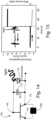
- the potential V GS between the gate terminal 140 and the source terminal 120 is subject to a variation. Then the semiconductor channel layer 110 impedance Z varies according to a characteristic curve like the one plotted in figure 9 .
- the RFID transmitter state is then switched from high-impedance (0 logic state) to low-impedance (1 logic state), as shown in said figure 9 .
- the impedance Z decreases considerably, allowing the change of the logic state, if measured in voltage, between the source 120 and the drain 130 electrodes of the field effect device 100.
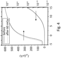
- Figures 10a and 10b show the transfer characteristics of a field effect device 100 and its frequency response.
- said figures 10a and 10b there are respectively plotted the drain currents and the gate currents as a function of gate-source voltage, at different drain voltages, and the gate capacity (in picoFarad) C G as a function of the gate-source voltage V GS , at different frequencies.
- the voltage at the gate electrode 140 remains constant, thus leaving unaltered the impedance Z probed by the RFID chip 401.
- the occurrence of the sensing event is stored in a passive memory state, as better explained below, where some applications of the field effect device 100 are examined, particularly directed toward the application of the RFID devices, for which, as it is well known, high sensitive devices are required to improve the detection sensitivity.
- the device 100 is operated close to threshold, therefore even small voltage variations normally between the gate electrode 140 and the source electrode 120 lead to large variations in semiconductor channel 110 impedance that are directly detected by the RFID sensor 400 terminals.
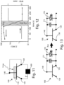
- Figure 11 shows the field effect device 100, according to the first embodiment, where a RFID transmitter 400 is connected between the source electrode 120 and the drain electrode 130, then parallel with the semiconductor channel layer 110.
- the source electrode 120 is also connected with the gate electrode 140.
- This logic switch configuration is read by RFID transmitter 400, which transmits an RFID receiver RFID-R, by the related antenna 402.
- the sensing means comprises a photodiode 170 and a capacitor 171, both parallel connected to said gate electrode 140 and said source electrode 120.
- FIG. 15 shows the variation of the impedance of the semiconductor channel layer 110 and the consequent RFID chip 401 logic state switch as a function of time.
- Figures 16a and 16b show a second example of the field effect device, which does not form part of the present invention, wherein the sensing means of said field effect device 100 comprises a capacity 171, connected between said gate electrode 140 and said source electrode 120, and a rectifier diode 172, series connected with a piezoelectric sensor 173, connected to said gate electrode 140 and to said source electrode 120.
- the sensing means of said field effect device 100 comprises a capacity 171, connected between said gate electrode 140 and said source electrode 120, and a rectifier diode 172, series connected with a piezoelectric sensor 173, connected to said gate electrode 140 and to said source electrode 120.
- sensing means comprises a capacitor 171 and a pyroelectric sensor 174, capable of sensing the environment temperature.
- the capacitor 171 and said pyroelectric sensor 174 are series connected.
- Said sensing means are connected between the gate electrode 140 and the source electrode 120, as the other embodiments above described.
- V GS Variation of the gate - source potential causes the variation of the impedance Z of the semiconductor channel layer 110.
- a fourth example of the field effect device is shown, which does not form part of the present invention, wherein the sensor means now comprises a capacitor 171 and a chemical sensor 175.
- the connection of said chemical sensor 175 and said capacitor 171 is the same the third example described above.
- the electrical operation is the same of the third example shown in figures 17a and 17b , with the apparent difference that in that case it is a chemical substance detection, as sensing event, that changes the electrical state of the sensor and then the gate - source voltage, so as to change the impedance between said source electrode 120 and said drain electrode 130.
- a RFID chip 401 can be connected between said source electrode 120 and said drain electrode 130, so as to detect the variation of the potential between said electrodes, in transmitting the states change, namely the detection of ionization radiation, light, mechanical stress, variation of temperature and detection of chemical substances to a RFID receiver RFID-R.
- An advantage of the field effect device is that of enabling to create low-cost RFID sensors capable of monitoring if ionizing radiation goes beyond a defined threshold. Once conditions are beyond threshold, the RFID sensor state is changed and the event can be traced at a later time using a wireless RFID readout systems.
- a further advantage of the device according to the invention is that of introducing innovative nanostructured materials allowing to combine unique electronic sensor performance, with the possibility to deposit sensors in microstructured arrays on large-areas and on flexible plastic substrates.
Landscapes
- Health & Medical Sciences (AREA)
- Life Sciences & Earth Sciences (AREA)
- Physics & Mathematics (AREA)
- General Physics & Mathematics (AREA)
- Chemical & Material Sciences (AREA)
- Molecular Biology (AREA)
- Microelectronics & Electronic Packaging (AREA)
- Engineering & Computer Science (AREA)
- Spectroscopy & Molecular Physics (AREA)
- High Energy & Nuclear Physics (AREA)
- Chemical Kinetics & Catalysis (AREA)
- Electrochemistry (AREA)
- Analytical Chemistry (AREA)
- Biochemistry (AREA)
- General Health & Medical Sciences (AREA)
- Immunology (AREA)
- Pathology (AREA)
- Thin Film Transistor (AREA)
Claims (14)
- Erkennender Sensor mit:ein Substrat (160);eine Vielzahl von ionisationssensitiven Feldeffektvorrichtungen (100), die auf dem Substrat (160) angeordnet sind, wobei jedes der ionisationssensitiven Feldeffektvorrichtungen (100) Folgendes umfassteinen Halbleiterkanal (110), wobei der Halbleiterkanal (110) eine Schicht ist und aus einem amorphen Oxid hergestellt ist,eine Source-Elektrode (120), die mit dem Halbleiterkanal (110) verbunden ist,eine Drain-Elektrode (130), die mit dem Halbleiterkanal (110) verbunden ist, so dass der Halbleiterkanal (110) zwischen der Source-Elektrode (120) und der Drain-Elektrode (130) angeordnet ist,eine Gate-Elektrode (140) mit einer Gate-Kapazität (CG ), wobei die Gate-Kapazität (CG ) eine Funktion der Gate-Source-Spannung (VGS ) bei verschiedenen Frequenzen ist, undeine dielektrische Schicht (150),die zwischen der Gate-Elektrode (140) und dem Halbleiterkanal (110) angeordnet ist,wobei die dielektrische Schicht (150) so angeordnet ist, dass sie einer ionisierenden Strahlung, wie Röntgenstrahlen und dergleichen, ausgesetzt werden kann, wobei die Gate-Elektrode (140) mindestens eine Hauptschicht umfasst, die aus mindestens einem Material besteht, das mindestens ein Kationselement mit einer Atomzahl aufweist, die so gewählt ist, dass sie die Absorption der einfallenden, zu erfassenden ionisierenden Strahlung erhöht, undwobei das mindestens ein Material der dielektrischen Schicht (150) eine hohe Ordnungszahl Z aufweist, wobei die Ordnungszahl Z höher als 36 (Z>36) ist; undmindestens einen RFID-Sender (400) mit einem Paar von Elektroden, die mit der Source-Elektrode (120) und der Gate-Elektrode (140) eines zugehörigen Feldeffekt-Bauelements (100) verbunden sind, das so konfiguriert ist, dass es mit einem RFID-Empfänger (RFID-R) verbunden werden kann;wobei der RFID-Sender (400) seinen Zustand bei einem Ionisierungsereignis von einem ersten logischen Zustand hoher Impedanz in einen zweiten logischen Zustand niedriger Impedanz umschaltet und die Zustandsänderung an den RFID-Empfänger (RFID-R) überträgt.
- Sensor nach dem vorhergehenden Anspruch, dadurch gekennzeichnet, dass das amorphe Oxid vom Typ des amorphen Oxids mit hoher Mobilität ist und aus der Gruppe ausgewählt ist, die umfasst: Indium-Gallium-Zink-Oxid (IGZO) und/oder Indium-Hafnium-Zink-Oxid (IHZO) und/oder Zink-Zinn-Oxid (ZTO) und/oder Gallium-Zink-Zinn-Oxid (GZTO).
- Sensor nach einem der vorhergehenden Ansprüche, dadurch gekennzeichnet, dass die mindestens eine Hauptschicht der dielektrischen Schicht (150) aus Yttriumoxid (Y2O3) und/oder Zirkoniumoxid (ZrO2) und/oder Hafniumoxid (HfO2) und/oder Tantalpentoxid (Ta2O5) und/oder Bismutoxid (Bi2O3) besteht.
- Sensor nach einem der vorhergehenden Ansprüche, dadurch gekennzeichnet, dass die dielektrische Schicht (150) jeder der Vorrichtungen (100) in elektrischem Kontakt mit der Source-Elektrode (120) und der Drain-Elektrode (130) steht.
- Sensor nach einem der vorhergehenden Ansprüche, dadurch gekennzeichnet, dass die dielektrische Schicht (150) jeder der Vorrichtungen (100) eine Dicke größer oder gleich 150 nm aufweist.
- Sensor nach einem der vorhergehenden Ansprüche, dadurch gekennzeichnet, dass die dielektrische Schicht (150) jeder der Vorrichtungen (100) eine Mehrschicht ist, die eine oder mehrere isolierende Schichten mit einer niedrigeren Ordnungszahl als die Ordnungszahl der Hauptschicht umfasst.
- Sensor nach dem vorhergehenden Anspruch, dadurch gekennzeichnet, dass die eine oder mehreren Isolierschichten der dielektrischen Schicht (150) jeder der Vorrichtungen (100) aus Siliziumdioxid (SiO2) und/oder Aluminiumoxid (Al2O3) hergestellt sind.
- Sensor nach einem der Ansprüche 6 oder 7, dadurch gekennzeichnet, dass die dielektrische Schicht (150) jeder der Vorrichtungen (100) Folgendes umfasstdie Kombination aus der Isolierschicht mit Atomen niedrigerer Ordnungszahl und der Hauptschicht zwei- bis zehnmal wiederholt wird, undeine obere Schicht der genannten Isolierschicht mit Atomen niedrigerer Ordnungszahl.
- Sensor nach einem der vorhergehenden Ansprüche, dadurch gekennzeichnet, dass jede der Vorrichtungen (100) mindestens ein Substrat (160) umfasst, auf dem die Gate-Elektrode (140) und die dielektrische Schicht (150) aufgebracht sind.
- Vorrichtung (100) nach einem der vorhergehenden Ansprüche, dadurch gekennzeichnet, dass die Gate- (140), Source- (120) und Drain- (130) Elektroden jeder der Vorrichtungen (100) aus leitendem Material, wie Molybdän (Mo), Kupfer (Cu), Aluminium (Al), Gold (Au) und/oder Silber (Ag), und/oder leitenden Oxiden, wie Galliumdotiertem Zinkoxid (GZO) oder Indium-Zinkoxid (IZO) und/oder leitenden Polymeren, wie Pedot, hergestellt sind: Pss.
- Sensor nach einem der vorhergehenden Ansprüche, dadurch gekennzeichnet, dass das Substrat flexibel ist und vorzugsweise aus Polyethylennaphthalat besteht.
- Sensor nach einem der vorhergehenden Ansprüche, dadurch gekennzeichnet, dass die Feldeffektvorrichtungen (100) als Array oder als Matrix angeordnet sind.
- Sensor nach einem der vorhergehenden Ansprüche, dadurch gekennzeichnet, dass der RFID-Sender (400) einen RFID-Chip (401) und eine Antenne (402) umfasst.
- Sensor nach einem der vorhergehenden Ansprüche, dadurch gekennzeichnet, dass er eine Vielzahl von RFID-Sendern (400) umfasst, von denen jeder operativ mit einer zugehöriger Feldeffektvorrichtung (100) verbunden ist.
Applications Claiming Priority (2)
| Application Number | Priority Date | Filing Date | Title |
|---|---|---|---|
| PT8241216 | 2016-11-14 | ||
| PCT/IT2017/000050 WO2018087787A1 (en) | 2016-11-14 | 2017-03-14 | Sensitive field effect device and manufacturing method thereof |
Publications (3)
| Publication Number | Publication Date |
|---|---|
| EP3538883A1 EP3538883A1 (de) | 2019-09-18 |
| EP3538883C0 EP3538883C0 (de) | 2024-05-01 |
| EP3538883B1 true EP3538883B1 (de) | 2024-05-01 |
Family
ID=67551000
Family Applications (1)
| Application Number | Title | Priority Date | Filing Date |
|---|---|---|---|
| EP17719015.4A Active EP3538883B1 (de) | 2016-11-14 | 2017-03-14 | Sensitive feldeffektvorrichtung |
Country Status (1)
| Country | Link |
|---|---|
| EP (1) | EP3538883B1 (de) |
-
2017
- 2017-03-14 EP EP17719015.4A patent/EP3538883B1/de active Active
Non-Patent Citations (1)
| Title |
|---|
| CRAMER TOBIAS ET AL: "Passive radiofrequency x-ray dosimeter tag based on flexible radiation-sensitive oxide field-effect transistor", SCIENCE ADVANCES, vol. 4, no. 6, 29 June 2018 (2018-06-29), XP055929707, DOI: 10.1126/sciadv.aat1825 * |
Also Published As
| Publication number | Publication date |
|---|---|
| EP3538883C0 (de) | 2024-05-01 |
| EP3538883A1 (de) | 2019-09-18 |
Similar Documents
| Publication | Publication Date | Title |
|---|---|---|
| US11360044B2 (en) | Sensitive field effect device and manufacturing method thereof | |
| Street et al. | Amorphous silicon sensor arrays for radiation imaging | |
| Cramer et al. | Passive radiofrequency x-ray dosimeter tag based on flexible radiation-sensitive oxide field-effect transistor | |
| Cramer et al. | Radiation‐tolerant flexible large‐area electronics based on oxide semiconductors | |
| US8080805B2 (en) | FET radiation monitor | |
| US8981304B2 (en) | Radiation detector | |
| US9804273B2 (en) | Combined n-type and p-type MOS-based radiation sensors for environmental compensations | |
| CA1204885A (en) | Dosimeter | |
| CN114864609B (zh) | 有源像素传感器及平板探测器 | |
| CN108981910A (zh) | 光电探测电路以及光电探测器 | |
| US9213112B2 (en) | Neutron radiation sensor | |
| EP3232230B1 (de) | Vorrichtung zur erfassung von strahlung | |
| US20160148953A1 (en) | Array substrate, radiation detector, and wiring substrate | |
| US8581203B2 (en) | Radiation detecting device and method of operating | |
| WO2010046904A2 (en) | Method and device for determining ionizing radiation | |
| EP3538883A1 (de) | Sensitive feldeffektvorrichtung und herstellungsverfahren dafür | |
| EP0381517B1 (de) | Strahlungsdetektor | |
| US11300444B2 (en) | Photoelectric detection circuit and photoelectric detector | |
| US20080258072A1 (en) | Detector for Ionizing Radiation | |
| Saha et al. | Flexible capacitive UV sensor for future wearables | |
| JP2002009268A (ja) | 放射線検出装置 | |
| Bordoni et al. | Dielectric multilayers impact on radiation-induced charge accumulation in highly sensitive oxide field effect transistors | |
| CN114637039A (zh) | 一种针对总剂量效应损失的半导体辐照探测器 | |
| Вікулин et al. | DETECTORS BASED ON FIELD EFFECT TRANSISTORS | |
| CN118654767A (zh) | 一种基于双晶体管结构的超快光信号检测方法 |
Legal Events
| Date | Code | Title | Description |
|---|---|---|---|
| STAA | Information on the status of an ep patent application or granted ep patent |
Free format text: STATUS: UNKNOWN |
|
| STAA | Information on the status of an ep patent application or granted ep patent |
Free format text: STATUS: THE INTERNATIONAL PUBLICATION HAS BEEN MADE |
|
| PUAI | Public reference made under article 153(3) epc to a published international application that has entered the european phase |
Free format text: ORIGINAL CODE: 0009012 |
|
| STAA | Information on the status of an ep patent application or granted ep patent |
Free format text: STATUS: REQUEST FOR EXAMINATION WAS MADE |
|
| 17P | Request for examination filed |
Effective date: 20190530 |
|
| AK | Designated contracting states |
Kind code of ref document: A1 Designated state(s): AL AT BE BG CH CY CZ DE DK EE ES FI FR GB GR HR HU IE IS IT LI LT LU LV MC MK MT NL NO PL PT RO RS SE SI SK SM TR |
|
| AX | Request for extension of the european patent |
Extension state: BA ME |
|
| DAV | Request for validation of the european patent (deleted) | ||
| DAX | Request for extension of the european patent (deleted) | ||
| STAA | Information on the status of an ep patent application or granted ep patent |
Free format text: STATUS: EXAMINATION IS IN PROGRESS |
|
| 17Q | First examination report despatched |
Effective date: 20200820 |
|
| GRAP | Despatch of communication of intention to grant a patent |
Free format text: ORIGINAL CODE: EPIDOSNIGR1 |
|
| STAA | Information on the status of an ep patent application or granted ep patent |
Free format text: STATUS: GRANT OF PATENT IS INTENDED |
|
| INTG | Intention to grant announced |
Effective date: 20240103 |
|
| GRAS | Grant fee paid |
Free format text: ORIGINAL CODE: EPIDOSNIGR3 |
|
| GRAA | (expected) grant |
Free format text: ORIGINAL CODE: 0009210 |
|
| STAA | Information on the status of an ep patent application or granted ep patent |
Free format text: STATUS: THE PATENT HAS BEEN GRANTED |
|
| AK | Designated contracting states |
Kind code of ref document: B1 Designated state(s): AL AT BE BG CH CY CZ DE DK EE ES FI FR GB GR HR HU IE IS IT LI LT LU LV MC MK MT NL NO PL PT RO RS SE SI SK SM TR |
|
| REG | Reference to a national code |
Ref country code: GB Ref legal event code: FG4D |
|
| REG | Reference to a national code |
Ref country code: CH Ref legal event code: EP |
|
| REG | Reference to a national code |
Ref country code: IE Ref legal event code: FG4D |
|
| REG | Reference to a national code |
Ref country code: DE Ref legal event code: R096 Ref document number: 602017081520 Country of ref document: DE |
|
| U01 | Request for unitary effect filed |
Effective date: 20240530 |
|
| U07 | Unitary effect registered |
Designated state(s): AT BE BG DE DK EE FI FR IT LT LU LV MT NL PT SE SI Effective date: 20240607 |
|
| PG25 | Lapsed in a contracting state [announced via postgrant information from national office to epo] |
Ref country code: IS Free format text: LAPSE BECAUSE OF FAILURE TO SUBMIT A TRANSLATION OF THE DESCRIPTION OR TO PAY THE FEE WITHIN THE PRESCRIBED TIME-LIMIT Effective date: 20240901 |
|
| PG25 | Lapsed in a contracting state [announced via postgrant information from national office to epo] |
Ref country code: HR Free format text: LAPSE BECAUSE OF FAILURE TO SUBMIT A TRANSLATION OF THE DESCRIPTION OR TO PAY THE FEE WITHIN THE PRESCRIBED TIME-LIMIT Effective date: 20240501 |
|
| PG25 | Lapsed in a contracting state [announced via postgrant information from national office to epo] |
Ref country code: ES Free format text: LAPSE BECAUSE OF FAILURE TO SUBMIT A TRANSLATION OF THE DESCRIPTION OR TO PAY THE FEE WITHIN THE PRESCRIBED TIME-LIMIT Effective date: 20240501 |
|
| PG25 | Lapsed in a contracting state [announced via postgrant information from national office to epo] |
Ref country code: PL Free format text: LAPSE BECAUSE OF FAILURE TO SUBMIT A TRANSLATION OF THE DESCRIPTION OR TO PAY THE FEE WITHIN THE PRESCRIBED TIME-LIMIT Effective date: 20240501 |
|
| PG25 | Lapsed in a contracting state [announced via postgrant information from national office to epo] |
Ref country code: PL Free format text: LAPSE BECAUSE OF FAILURE TO SUBMIT A TRANSLATION OF THE DESCRIPTION OR TO PAY THE FEE WITHIN THE PRESCRIBED TIME-LIMIT Effective date: 20240501 Ref country code: NO Free format text: LAPSE BECAUSE OF FAILURE TO SUBMIT A TRANSLATION OF THE DESCRIPTION OR TO PAY THE FEE WITHIN THE PRESCRIBED TIME-LIMIT Effective date: 20240801 Ref country code: IS Free format text: LAPSE BECAUSE OF FAILURE TO SUBMIT A TRANSLATION OF THE DESCRIPTION OR TO PAY THE FEE WITHIN THE PRESCRIBED TIME-LIMIT Effective date: 20240901 Ref country code: HR Free format text: LAPSE BECAUSE OF FAILURE TO SUBMIT A TRANSLATION OF THE DESCRIPTION OR TO PAY THE FEE WITHIN THE PRESCRIBED TIME-LIMIT Effective date: 20240501 Ref country code: ES Free format text: LAPSE BECAUSE OF FAILURE TO SUBMIT A TRANSLATION OF THE DESCRIPTION OR TO PAY THE FEE WITHIN THE PRESCRIBED TIME-LIMIT Effective date: 20240501 Ref country code: RS Free format text: LAPSE BECAUSE OF FAILURE TO SUBMIT A TRANSLATION OF THE DESCRIPTION OR TO PAY THE FEE WITHIN THE PRESCRIBED TIME-LIMIT Effective date: 20240801 |
|
| PG25 | Lapsed in a contracting state [announced via postgrant information from national office to epo] |
Ref country code: CZ Free format text: LAPSE BECAUSE OF FAILURE TO SUBMIT A TRANSLATION OF THE DESCRIPTION OR TO PAY THE FEE WITHIN THE PRESCRIBED TIME-LIMIT Effective date: 20240501 |
|
| PG25 | Lapsed in a contracting state [announced via postgrant information from national office to epo] |
Ref country code: SK Free format text: LAPSE BECAUSE OF FAILURE TO SUBMIT A TRANSLATION OF THE DESCRIPTION OR TO PAY THE FEE WITHIN THE PRESCRIBED TIME-LIMIT Effective date: 20240501 Ref country code: RO Free format text: LAPSE BECAUSE OF FAILURE TO SUBMIT A TRANSLATION OF THE DESCRIPTION OR TO PAY THE FEE WITHIN THE PRESCRIBED TIME-LIMIT Effective date: 20240501 |
|
| PG25 | Lapsed in a contracting state [announced via postgrant information from national office to epo] |
Ref country code: SM Free format text: LAPSE BECAUSE OF FAILURE TO SUBMIT A TRANSLATION OF THE DESCRIPTION OR TO PAY THE FEE WITHIN THE PRESCRIBED TIME-LIMIT Effective date: 20240501 |
|
| PG25 | Lapsed in a contracting state [announced via postgrant information from national office to epo] |
Ref country code: SM Free format text: LAPSE BECAUSE OF FAILURE TO SUBMIT A TRANSLATION OF THE DESCRIPTION OR TO PAY THE FEE WITHIN THE PRESCRIBED TIME-LIMIT Effective date: 20240501 Ref country code: SK Free format text: LAPSE BECAUSE OF FAILURE TO SUBMIT A TRANSLATION OF THE DESCRIPTION OR TO PAY THE FEE WITHIN THE PRESCRIBED TIME-LIMIT Effective date: 20240501 Ref country code: RO Free format text: LAPSE BECAUSE OF FAILURE TO SUBMIT A TRANSLATION OF THE DESCRIPTION OR TO PAY THE FEE WITHIN THE PRESCRIBED TIME-LIMIT Effective date: 20240501 Ref country code: CZ Free format text: LAPSE BECAUSE OF FAILURE TO SUBMIT A TRANSLATION OF THE DESCRIPTION OR TO PAY THE FEE WITHIN THE PRESCRIBED TIME-LIMIT Effective date: 20240501 |
|
| REG | Reference to a national code |
Ref country code: DE Ref legal event code: R097 Ref document number: 602017081520 Country of ref document: DE |
|
| PLBE | No opposition filed within time limit |
Free format text: ORIGINAL CODE: 0009261 |
|
| STAA | Information on the status of an ep patent application or granted ep patent |
Free format text: STATUS: NO OPPOSITION FILED WITHIN TIME LIMIT |
|
| 26N | No opposition filed |
Effective date: 20250204 |
|
| U20 | Renewal fee for the european patent with unitary effect paid |
Year of fee payment: 9 Effective date: 20250331 |
|
| PG25 | Lapsed in a contracting state [announced via postgrant information from national office to epo] |
Ref country code: MC Free format text: LAPSE BECAUSE OF FAILURE TO SUBMIT A TRANSLATION OF THE DESCRIPTION OR TO PAY THE FEE WITHIN THE PRESCRIBED TIME-LIMIT Effective date: 20240501 |
|
| REG | Reference to a national code |
Ref country code: CH Ref legal event code: H13 Free format text: ST27 STATUS EVENT CODE: U-0-0-H10-H13 (AS PROVIDED BY THE NATIONAL OFFICE) Effective date: 20251023 |
|
| GBPC | Gb: european patent ceased through non-payment of renewal fee |
Effective date: 20250314 |
|
| PG25 | Lapsed in a contracting state [announced via postgrant information from national office to epo] |
Ref country code: GB Free format text: LAPSE BECAUSE OF NON-PAYMENT OF DUE FEES Effective date: 20250314 |
|
| PG25 | Lapsed in a contracting state [announced via postgrant information from national office to epo] |
Ref country code: CH Free format text: LAPSE BECAUSE OF NON-PAYMENT OF DUE FEES Effective date: 20250331 |
|
| PG25 | Lapsed in a contracting state [announced via postgrant information from national office to epo] |
Ref country code: IE Free format text: LAPSE BECAUSE OF NON-PAYMENT OF DUE FEES Effective date: 20250314 |
|
| U20 | Renewal fee for the european patent with unitary effect paid |
Year of fee payment: 10 Effective date: 20260112 |