EP3537854A1 - Circuit board, electronic circuit device, and production method of circuit board - Google Patents
Circuit board, electronic circuit device, and production method of circuit board Download PDFInfo
- Publication number
- EP3537854A1 EP3537854A1 EP19161025.2A EP19161025A EP3537854A1 EP 3537854 A1 EP3537854 A1 EP 3537854A1 EP 19161025 A EP19161025 A EP 19161025A EP 3537854 A1 EP3537854 A1 EP 3537854A1
- Authority
- EP
- European Patent Office
- Prior art keywords
- conductive
- hole
- circuit board
- substrate
- conductive part
- Prior art date
- Legal status (The legal status is an assumption and is not a legal conclusion. Google has not performed a legal analysis and makes no representation as to the accuracy of the status listed.)
- Granted
Links
Images



Classifications
-
- H—ELECTRICITY
- H05—ELECTRIC TECHNIQUES NOT OTHERWISE PROVIDED FOR
- H05K—PRINTED CIRCUITS; CASINGS OR CONSTRUCTIONAL DETAILS OF ELECTRIC APPARATUS; MANUFACTURE OF ASSEMBLAGES OF ELECTRICAL COMPONENTS
- H05K1/00—Printed circuits
- H05K1/02—Details
- H05K1/09—Use of materials for the conductive, e.g. metallic pattern
- H05K1/092—Dispersed materials, e.g. conductive pastes or inks
- H05K1/097—Inks comprising nanoparticles and specially adapted for being sintered at low temperature
-
- H—ELECTRICITY
- H05—ELECTRIC TECHNIQUES NOT OTHERWISE PROVIDED FOR
- H05K—PRINTED CIRCUITS; CASINGS OR CONSTRUCTIONAL DETAILS OF ELECTRIC APPARATUS; MANUFACTURE OF ASSEMBLAGES OF ELECTRICAL COMPONENTS
- H05K3/00—Apparatus or processes for manufacturing printed circuits
- H05K3/40—Forming printed elements for providing electric connections to or between printed circuits
- H05K3/4038—Through-connections; Vertical interconnect access [VIA] connections
- H05K3/4053—Through-connections; Vertical interconnect access [VIA] connections by thick-film techniques
- H05K3/4069—Through-connections; Vertical interconnect access [VIA] connections by thick-film techniques for via connections in organic insulating substrates
-
- H—ELECTRICITY
- H05—ELECTRIC TECHNIQUES NOT OTHERWISE PROVIDED FOR
- H05K—PRINTED CIRCUITS; CASINGS OR CONSTRUCTIONAL DETAILS OF ELECTRIC APPARATUS; MANUFACTURE OF ASSEMBLAGES OF ELECTRICAL COMPONENTS
- H05K1/00—Printed circuits
- H05K1/02—Details
- H05K1/09—Use of materials for the conductive, e.g. metallic pattern
-
- H—ELECTRICITY
- H05—ELECTRIC TECHNIQUES NOT OTHERWISE PROVIDED FOR
- H05K—PRINTED CIRCUITS; CASINGS OR CONSTRUCTIONAL DETAILS OF ELECTRIC APPARATUS; MANUFACTURE OF ASSEMBLAGES OF ELECTRICAL COMPONENTS
- H05K1/00—Printed circuits
- H05K1/02—Details
- H05K1/11—Printed elements for providing electric connections to or between printed circuits
- H05K1/115—Via connections; Lands around holes or via connections
- H05K1/116—Lands, clearance holes or other lay-out details concerning the surrounding of a via
-
- H—ELECTRICITY
- H05—ELECTRIC TECHNIQUES NOT OTHERWISE PROVIDED FOR
- H05K—PRINTED CIRCUITS; CASINGS OR CONSTRUCTIONAL DETAILS OF ELECTRIC APPARATUS; MANUFACTURE OF ASSEMBLAGES OF ELECTRICAL COMPONENTS
- H05K1/00—Printed circuits
- H05K1/02—Details
- H05K1/11—Printed elements for providing electric connections to or between printed circuits
- H05K1/118—Printed elements for providing electric connections to or between printed circuits specially for flexible printed circuits, e.g. using folded portions
-
- H—ELECTRICITY
- H05—ELECTRIC TECHNIQUES NOT OTHERWISE PROVIDED FOR
- H05K—PRINTED CIRCUITS; CASINGS OR CONSTRUCTIONAL DETAILS OF ELECTRIC APPARATUS; MANUFACTURE OF ASSEMBLAGES OF ELECTRICAL COMPONENTS
- H05K3/00—Apparatus or processes for manufacturing printed circuits
- H05K3/10—Apparatus or processes for manufacturing printed circuits in which conductive material is applied to the insulating support in such a manner as to form the desired conductive pattern
- H05K3/12—Apparatus or processes for manufacturing printed circuits in which conductive material is applied to the insulating support in such a manner as to form the desired conductive pattern using thick film techniques, e.g. printing techniques to apply the conductive material or similar techniques for applying conductive paste or ink patterns
- H05K3/1283—After-treatment of the printed patterns, e.g. sintering or curing methods
-
- H—ELECTRICITY
- H05—ELECTRIC TECHNIQUES NOT OTHERWISE PROVIDED FOR
- H05K—PRINTED CIRCUITS; CASINGS OR CONSTRUCTIONAL DETAILS OF ELECTRIC APPARATUS; MANUFACTURE OF ASSEMBLAGES OF ELECTRICAL COMPONENTS
- H05K3/00—Apparatus or processes for manufacturing printed circuits
- H05K3/40—Forming printed elements for providing electric connections to or between printed circuits
- H05K3/4038—Through-connections; Vertical interconnect access [VIA] connections
-
- H—ELECTRICITY
- H05—ELECTRIC TECHNIQUES NOT OTHERWISE PROVIDED FOR
- H05K—PRINTED CIRCUITS; CASINGS OR CONSTRUCTIONAL DETAILS OF ELECTRIC APPARATUS; MANUFACTURE OF ASSEMBLAGES OF ELECTRICAL COMPONENTS
- H05K3/00—Apparatus or processes for manufacturing printed circuits
- H05K3/40—Forming printed elements for providing electric connections to or between printed circuits
- H05K3/4038—Through-connections; Vertical interconnect access [VIA] connections
- H05K3/4053—Through-connections; Vertical interconnect access [VIA] connections by thick-film techniques
- H05K3/4061—Through-connections; Vertical interconnect access [VIA] connections by thick-film techniques for via connections in inorganic insulating substrates
-
- H—ELECTRICITY
- H05—ELECTRIC TECHNIQUES NOT OTHERWISE PROVIDED FOR
- H05K—PRINTED CIRCUITS; CASINGS OR CONSTRUCTIONAL DETAILS OF ELECTRIC APPARATUS; MANUFACTURE OF ASSEMBLAGES OF ELECTRICAL COMPONENTS
- H05K1/00—Printed circuits
- H05K1/02—Details
- H05K1/03—Use of materials for the substrate
- H05K1/0393—Flexible materials
-
- H—ELECTRICITY
- H05—ELECTRIC TECHNIQUES NOT OTHERWISE PROVIDED FOR
- H05K—PRINTED CIRCUITS; CASINGS OR CONSTRUCTIONAL DETAILS OF ELECTRIC APPARATUS; MANUFACTURE OF ASSEMBLAGES OF ELECTRICAL COMPONENTS
- H05K2201/00—Indexing scheme relating to printed circuits covered by H05K1/00
- H05K2201/02—Fillers; Particles; Fibers; Reinforcement materials
- H05K2201/0203—Fillers and particles
- H05K2201/0242—Shape of an individual particle
- H05K2201/0257—Nanoparticles
-
- H—ELECTRICITY
- H05—ELECTRIC TECHNIQUES NOT OTHERWISE PROVIDED FOR
- H05K—PRINTED CIRCUITS; CASINGS OR CONSTRUCTIONAL DETAILS OF ELECTRIC APPARATUS; MANUFACTURE OF ASSEMBLAGES OF ELECTRICAL COMPONENTS
- H05K2201/00—Indexing scheme relating to printed circuits covered by H05K1/00
- H05K2201/02—Fillers; Particles; Fibers; Reinforcement materials
- H05K2201/0203—Fillers and particles
- H05K2201/0263—Details about a collection of particles
- H05K2201/0266—Size distribution
-
- H—ELECTRICITY
- H05—ELECTRIC TECHNIQUES NOT OTHERWISE PROVIDED FOR
- H05K—PRINTED CIRCUITS; CASINGS OR CONSTRUCTIONAL DETAILS OF ELECTRIC APPARATUS; MANUFACTURE OF ASSEMBLAGES OF ELECTRICAL COMPONENTS
- H05K2201/00—Indexing scheme relating to printed circuits covered by H05K1/00
- H05K2201/02—Fillers; Particles; Fibers; Reinforcement materials
- H05K2201/0203—Fillers and particles
- H05K2201/0263—Details about a collection of particles
- H05K2201/0272—Mixed conductive particles, i.e. using different conductive particles, e.g. differing in shape
-
- H—ELECTRICITY
- H05—ELECTRIC TECHNIQUES NOT OTHERWISE PROVIDED FOR
- H05K—PRINTED CIRCUITS; CASINGS OR CONSTRUCTIONAL DETAILS OF ELECTRIC APPARATUS; MANUFACTURE OF ASSEMBLAGES OF ELECTRICAL COMPONENTS
- H05K2201/00—Indexing scheme relating to printed circuits covered by H05K1/00
- H05K2201/09—Shape and layout
- H05K2201/09209—Shape and layout details of conductors
- H05K2201/095—Conductive through-holes or vias
- H05K2201/09563—Metal filled via
-
- H—ELECTRICITY
- H05—ELECTRIC TECHNIQUES NOT OTHERWISE PROVIDED FOR
- H05K—PRINTED CIRCUITS; CASINGS OR CONSTRUCTIONAL DETAILS OF ELECTRIC APPARATUS; MANUFACTURE OF ASSEMBLAGES OF ELECTRICAL COMPONENTS
- H05K2203/00—Indexing scheme relating to apparatus or processes for manufacturing printed circuits covered by H05K3/00
- H05K2203/10—Using electric, magnetic and electromagnetic fields; Using laser light
- H05K2203/107—Using laser light
-
- H—ELECTRICITY
- H05—ELECTRIC TECHNIQUES NOT OTHERWISE PROVIDED FOR
- H05K—PRINTED CIRCUITS; CASINGS OR CONSTRUCTIONAL DETAILS OF ELECTRIC APPARATUS; MANUFACTURE OF ASSEMBLAGES OF ELECTRICAL COMPONENTS
- H05K2203/00—Indexing scheme relating to apparatus or processes for manufacturing printed circuits covered by H05K3/00
- H05K2203/11—Treatments characterised by their effect, e.g. heating, cooling, roughening
- H05K2203/1131—Sintering, i.e. fusing of metal particles to achieve or improve electrical conductivity
-
- H—ELECTRICITY
- H05—ELECTRIC TECHNIQUES NOT OTHERWISE PROVIDED FOR
- H05K—PRINTED CIRCUITS; CASINGS OR CONSTRUCTIONAL DETAILS OF ELECTRIC APPARATUS; MANUFACTURE OF ASSEMBLAGES OF ELECTRICAL COMPONENTS
- H05K2203/00—Indexing scheme relating to apparatus or processes for manufacturing printed circuits covered by H05K3/00
- H05K2203/14—Related to the order of processing steps
- H05K2203/1476—Same or similar kind of process performed in phases, e.g. coarse patterning followed by fine patterning
-
- H—ELECTRICITY
- H05—ELECTRIC TECHNIQUES NOT OTHERWISE PROVIDED FOR
- H05K—PRINTED CIRCUITS; CASINGS OR CONSTRUCTIONAL DETAILS OF ELECTRIC APPARATUS; MANUFACTURE OF ASSEMBLAGES OF ELECTRICAL COMPONENTS
- H05K2203/00—Indexing scheme relating to apparatus or processes for manufacturing printed circuits covered by H05K3/00
- H05K2203/14—Related to the order of processing steps
- H05K2203/1484—Simultaneous treatments, e.g. soldering lead-in-hole components simultaneously with surface mounted components
-
- H—ELECTRICITY
- H05—ELECTRIC TECHNIQUES NOT OTHERWISE PROVIDED FOR
- H05K—PRINTED CIRCUITS; CASINGS OR CONSTRUCTIONAL DETAILS OF ELECTRIC APPARATUS; MANUFACTURE OF ASSEMBLAGES OF ELECTRICAL COMPONENTS
- H05K3/00—Apparatus or processes for manufacturing printed circuits
- H05K3/10—Apparatus or processes for manufacturing printed circuits in which conductive material is applied to the insulating support in such a manner as to form the desired conductive pattern
- H05K3/12—Apparatus or processes for manufacturing printed circuits in which conductive material is applied to the insulating support in such a manner as to form the desired conductive pattern using thick film techniques, e.g. printing techniques to apply the conductive material or similar techniques for applying conductive paste or ink patterns
- H05K3/1216—Apparatus or processes for manufacturing printed circuits in which conductive material is applied to the insulating support in such a manner as to form the desired conductive pattern using thick film techniques, e.g. printing techniques to apply the conductive material or similar techniques for applying conductive paste or ink patterns by screen printing or stencil printing
Definitions
- the present invention relates to a circuit board provided with a through-hole that establishes electrical connection between wiring patterns formed respectively on both sides of a substrate.
- FIGs. 7 and 8 show examples of such circuit board as described above, and the through-hole 101 of the substrate 100 on which a copper foil 102 is formed as a wiring pattern is filled with conductive resin 103, then heated and cured, whereby the frontside and the backside of the substrate are electrically connected.
- the through-hole is filled with a conductive resin paste, then conductive particles therein are sintered to induce fusion, and a first conductive part is formed. Contraction of the first conductive part upon sintering generates a cavity in the center of the through-hole, and this cavity is embedded with another conductive resin paste to form a second conductive part where the conductive particles are resin-bonded. Accordingly, the first conductive part comprising the fusion-bonded conductive particles is provided along the inner surface of the through-hole, and the second conductive part where the conductive particles are resin-bonded fills the cavity in the center of the first conductive part.
- the circuit board described in the patent document 1 there exist in one through-hole, the first conductive part where conductive particles are sintered and the second conductive part where conductive particles are resin-bonded. Accordingly, cracking may occur on the boundaries therebetween, due to thermal shock or a similar event, and this may deteriorate conductivity, resulting in increase of a resistance value.
- a diameter of the through-hole is large, contraction upon curing the conductive resin paste placed in the center may make a dent on the bottom of the through-hole. Therefore, it is necessary to design the through-hole to have a small diameter.
- the present invention has been made in view of the aforementioned situations, and an objective of the present invention is to provide a circuit board with a through-hole, excellent in conductivity and heat dispersion, along with enhancing connection reliability on both sides of the substrate via the through-hole.
- a circuit board includes a substrate with a through-hole, a first conductive part covering an opening of the through-hole on one surface of the substrate in a manner blocking the opening, having a portion inserted into the through-hole from the one surface, and a second conductive part covering a second opening of the through-hole on the other surface of the substrate in a manner blocking the second opening, having a portion inserted into the through-hole from the other surface.
- the portion of the first conductive part inserted in the through-hole has a columnar shape having a diameter smaller than the through-hole.
- the portion of the second conductive part inserted in the through-hole has a shape that fills the gap between the columnar portion of the first conductive part and an inner surface of the through-hole.
- Both of the first and the second conductive parts comprise conductive particles being sintered.
- the circuit board thus configured is produced according to a following production method comprising four steps; a first step of filling a through-hole with a first conductive paste, from one surface of the substrate having the through-hole, the first conductive paste obtained by dispersing conductive particles in a solvent, a second step of forming a first conductive part having a portion inserted in the through-hole, the diameter of the portion being smaller than the through-hole, by heating the first conductive paste for contracting the first conductive paste along with sintering the conductive particles therein, a third step of filling a gap between an inner surface of the through-hole and the first conductive part, with a second conductive paste obtained by dispersing conductive particles in a solvent, from the other surface of the substrate, and a fourth step of forming a second conductive part filling the gap between the inner surface of the through-hole and the first conductive part, by heating the second conductive paste for contracting the second conductive paste along with sintering the conductive particles therein.
- the likelihood of so-called through-hole disconnection can be reduced, thereby enhancing connection reliability on both sides of the substrate via the through-hole.
- circuit board 1 relating to one embodiment of the present invention.
- the circuit board 1 of the present embodiment comprises, a substrate 11, a through-hole 12 provided in the substrate, a conductive part 13 filled in the through-hole 12, a frontside wiring pattern 14 provided on the frontside of the substrate 11, and a backside wiring pattern 15 provided on the backside of the substrate 11.
- the through-hole 12 is formed through the substrate 11 at a desired position, penetrating the frontside to the backside of the substrate 11.
- the conductive part 13 comprises a frontside conductive part 17 (a first conductive part 17) filled in the through-hole 12 and a backside conductive part 18 (a second conductive part 18).
- the frontside conductive part 17 (the first conductive part 17) covers the opening of the through-hole on the frontside of the substrate 11 in a manner blocking the opening, further comprising a frontside connection part 17A (a first connection part 17A) connected to the frontside wiring pattern 14, and a columnar part 17B formed continuously from the frontside connection part and provided vertically into the through-hole 12.
- the diameter of the columnar part 17B is smaller than the inner diameter of the through-hole 12.
- the frontside conductive part 17 (the first conductive part 17) and the frontside wiring pattern 14 may be formed as a single piece.
- the backside conductive part 18 (the second conductive part 18) covers the opening of the through-hole on the backside of the substrate 11 in a manner blocking the opening, further comprising a backside connection part 18A (a second connection part 18A) connected to the backside wiring pattern 15, and a shape 18B (hereinafter, referred to as a concave part 18B) bonded to the columnar part 17B within the through-hole 12 so as to fill the gap between the columnar part 17B and the inner surface of the through-hole 12.
- the backside conductive part 18 (the second conductive part 18) and the backside wiring pattern 15 may be formed as a single piece.
- Both of the frontside conductive part 17 and the backside conductive part 18 comprise conductive particles being sintered.
- the diameter of the columnar part 17B of the first conductive part 17 is smaller than the inner diameter of the through-hole and the second conductive part 18 has the shape to fill the gap between the inner surface of the through-hole 12 and the columnar part 17B. Therefore, the first conductive part 17 is bonded to the second conductive part 18, on both the circumference and the bottom of the columnar part 17B, and thus the area of joint is large.
- both the frontside conductive part 17 and the backside conductive part 18 comprise conductive particles being sintered, and this allows rigid bonding between the boundaries of the first conductive part 17 and the second conductive part 18 when sintering is performed. With this configuration, even when tension is applied to the through-hole and in proximity thereof, due to expansion and contraction of the substrate or a bend therein, thermal shock or environmental testing, and so on, the likelihood of through-hole disconnection and/or increase of resistance can be reduced.
- the first conductive part 17 in the center of the through-hole 12 is formed prior to forming the second conductive part 18 that fills the gap around the conductive part 17, whereby the width of the gap to be filled with the second conductive part 18 can be made smaller relative to the diameter of the first conductive part 17. Therefore, contraction of the second conductive part 18 upon sintering can be reduced, whereby gaps generated in the entire conductive part 13 may be minimized with respect to the through-hole 12. Since the contraction of the second conductive part 18 is small, this may avoid deformation such as dents on the bottom of the second conductive part 18, due to the contraction.
- frontside conductive part 17 and the backside conductive part 18 are defined just for the sake of convenience, and the frontside conductive part 17 may be arranged on the lower side, and the backside conductive part 18 may be arranged on the upper side.
- the first conductive part 17 may be obtained by sintering conductive nanoparticles having a diameter smaller than 1 ⁇ m, or obtained by sintering mixture of the conductive nanoparticles having a diameter smaller than 1 ⁇ m and conductive microparticles having a diameter equal to or greater than 1 ⁇ m and smaller than 1 mm.
- the second conductive part 18 may also be obtained by sintering conductive nanoparticles having a diameter smaller than 1 ⁇ m, or obtained by sintering mixture of the conductive nanoparticles having a diameter smaller than 1 ⁇ m and conductive microparticles having a diameter equal to or greater than 1 ⁇ m and smaller than 1 mm. It is to be noted that the diameter of the particle referred to here indicates an average diameter of the particle.
- an average diameter of the conductive particles of the first conductive part 17 before sintering is preferably equivalent to or smaller than the average diameter of the conductive particles of the second conductive part before sintering, because the smaller is the diameter, the larger contraction is induced when sintering is performed.
- the wiring patterns 14 and 15 may comprise sintered conductive particles. Furthermore, the substrate 11 may be flexible. Since the wiring patterns 14 and 15 are formed by sintering the conductive particles, making layers be porous, film peeling off or a similar event may hardly occur on the substrate, even though the substrate 11 is flexible.
- the through-hole 12 is formed passing through the substrate as shown in FIG. 2B , according to any method, for example, stamping, laser processing, and so on.
- the first conductive paste obtained by dispersing conductive particles in a solvent is prepared, the first conductive paste is applied to a predetermined region in proximity to the edge of the through-hole 12, using a method such as screen printing, from the frontside of the substrate 11, along with filling the through-hole 12.
- nanoparticles having a diameter smaller than 1 ⁇ m may be employed as the conductive particles for the first conductive paste, so as to cause volume contraction when sintering is performed.
- microparticles having a diameter between or equal to 1 ⁇ m and 100 ⁇ m may be contained partially. Those microparticles thus contained may reduce the volume contraction, but this may allow sintering of the conductive particles easily with keeping the shape of the first conductive paste, and this facilitates maintaining of the columnar shape.
- the proportion of nanoparticles having a diameter smaller than 1 ⁇ m in the conductive particles contained in the first conductive paste is preferably between or equal to 40 wt% and 100wt%, more preferably between or equal to 70 wt% and 100 wt%, and much more preferably between or equal to 75 wt% and 100 wt%.
- the proportion of the conductive particles in the first conductive paste is preferably between or equal to 50 wt% and 98 wt%, more preferably between or equal to 60 wt% and 95 wt%, and much more preferably between or equal to 80 wt% and 95 wt%.
- the conductive paste may contain, in addition to the solvent and the conductive particles, a dispersant such as polyvinylpyrrolidone, resin, and so on.
- a dispersant such as polyvinylpyrrolidone, resin, and so on.
- the resin e.g., epoxy resin, silicone resin, and urethane resin
- the dispersant should be added in small concentrations to a degree that may not hamper the dispersion.
- too low viscosity of the solvent may cause failure in keeping the shape when filled in the through-hole 12, and thus it is preferable to use the solvent with viscosity that enables keeping of the shape.
- the substrate the conductive particles, and the solvent will be described later.
- the first conductive paste is applied to the surface of the substrate 11, in the shape of the frontside wiring pattern 14 according to a method such as printing.
- an electromagnetic wave or heat is applied to the first conductive paste, thereby sintering the conductive particles within the conductive paste.
- a wavelength and other conditions in performing the sintering using the electromagnetic wave will be described later.
- the solvent contained in the conductive paste evaporates and the conductive particles are sintered (fused), and then, this causes volume contraction in the conductive paste. Therefore, the conductive paste applied to the proximity of the edge of the through-hole forms the frontside connection part 17A by sintering, and simultaneously, this sintering causes the volume contraction in the conductive paste filled in the through-hole 12 toward the center, separating from the inner surface of the through-hole 12, thereby forming the columnar part 17B.
- the conductive paste contracts by sintering, and the frontside conductive part 17 with a T-shaped cross section is formed, comprising the frontside connection part 17A and the columnar part 17B. Then, the gap 19 is generated between the inner surface of the through-hole 12 and the columnar part 17B.
- the through-hole 12 having a diameter of 300 ⁇ m was formed through the substrate 11 having a thickness of 100 ⁇ m, the through-hole was filled with the conductive paste where 85 wt% silver particles having an average diameter of 50 nm were dispersed in an organic solvent, and sintering was performed at 160°C to 200°C. Then, the diameter was contracted approximately by 10%, causing the gap 19.
- the first conductive paste in the through-hole 12 is also applied to the surface of the substrate 11, and then sintered to form the frontside wiring pattern 14.
- the second conductive paste is prepared to form the second conductive part 18.
- the proportion of nanoparticles having a diameter smaller than 1 ⁇ m in the conductive particles contained in the second conductive paste 18, is preferably between or equal to 0 wt% and 100wt%, more preferably between or equal to 0 wt% and 90 wt%, and much more preferably between or equal to 0 wt% and 80 wt%.
- the proportion of the conductive particles in the second conductive paste is preferably between or equal to 50 wt% and 98 wt%, more preferably between or equal to 60 wt% and 95 wt%, and much more preferably between or equal to 80 wt% and 95 wt%.
- the proportion of conductive microparticles can be higher than the conductive paste used for the frontside conductive part 17.
- the conductive paste used as the second conductive paste is the same as the first conductive paste.
- the second conductive paste is applied to a predetermined region in proximity to the edge of the through-hole 12, using a method such as screen printing, from the backside of the substrate 11, along with filling the gap 19 between the inner surface of the through-hole 12 and the columnar part 17B.
- the conductive paste serving as the backside wiring pattern 15 is also applied to the backside of the substrate 11.
- an electromagnetic wave or heat is applied to the second conductive paste, thereby sintering the conductive paste.
- the conductive paste applied to the proximity of the edge of the through-hole forms the backside connection part 18A
- the conductive paste filled in the gap between the inner surface of the through-hole 12 and the columnar part 17B is sintered to form the concave part 18B.
- Volume contraction occurs in the concave part 18B toward the center of the through-hole 12, whereby the concave part is rigidly bonded to the columnar part 17B.
- the conductive paste contracts by sintering, and the backside conductive part 18 is formed, comprising the backside connection part 18A and the concave part 18B.
- the second conductive paste applied to the surface of the substrate 11 in the shape of the wiring pattern is also sintered simultaneously with or continuously from heating the second conductive paste within the through-hole, thereby forming the backside wiring pattern 15.
- a range for applying the conductive paste to form the frontside connection part 17A and the backside connection part 18A should be set appropriately, considering a relationship with other electronic components to be mounted on the substrate 11 and wiring patterns.
- tension is likely to be concentrated on the edge of the through-hole 12. Therefore, it is preferable to determine the application range of the conductive paste to be applied to form the frontside connection part 17A and the backside connection part 18A, in a manner that contact positions respectively between the frontside connection part 17A and the frontside wiring pattern, and between the backside connection part 18A and the backside wiring pattern, should be set to the points less affected by the tension concentrated to the through-hole 12.
- the present embodiment a material with large volume contraction is used as the first conductive paste forming the first conductive part, and thus generated gap is filled with the second conductive paste from the backside and then sintered. Accordingly, the area of joint between the frontside conductive part and the backside conductive part is large, excellent in conductivity and heat dispersion, and therefore, this reduces a likelihood of so-called through-hole disconnection, and connection reliability on both sides of the substrate can be enhanced.
- the wiring pattern may be formed simultaneously with forming the through-hole, or it may be formed prior to or after forming the through-hole.
- any material may be used for the substrate 11, as far as the material is capable of supporting the first and the second conductive parts 17 and 18, and the wiring patterns 14 and 15, at least the surface thereof having insulation properties, and being resistant to sintering when the first and the second conductive parts 17 and 18 are formed.
- There may be employed, for example, a polyethylene terephthalate (PET) substrate, a polyethylene naphthalate (PEN) substrate, a polycarbonate (PC) substrate, a liquid crystal polymer, a glass epoxy substrate, a paper phenol substrate, a flexible print substrate, a ceramic substrate, a glass containing silicon substrate, a glass substrate, and a metal substrate having a surface coated with an insulating layer.
- PET polyethylene terephthalate
- PEN polyethylene naphthalate
- PC polycarbonate
- liquid crystal polymer a glass epoxy substrate
- paper phenol substrate phenol
- a flexible print substrate a ceramic substrate
- a glass containing silicon substrate a glass substrate
- At least one of the conductive metals such as Ag, Cu, Au, Pt, Ni, and Pd may be employed.
- organic solvents such as amine, alcohol, ether, aromatic compounds, ketone, and nitrile, and water may be employed.
- the substrate 11 can be formed with a thickness from about 100 nm to 3 mm.
- the diameter of the through-hole 12 may be between or equal to 5 ⁇ m and 1 mm.
- Electrical resistivity of the conductive part 13 within the through-hole is preferably 10 -4 ⁇ cm or less, and in particular, low resistance in the order of 10 -6 ⁇ cm is desirable.
- the electrical resistivity of the wiring patterns 14 and 15 is preferably 10 -4 ⁇ cm or less, and in particular, low resistance in the order of 10 -6 ⁇ cm is desirable.
- At least one of the following methods may be employed for sintering the conductive paste; sintering by irradiation of electromagnetic waves such as light, and sintering according to a method other than the irradiation of electromagnetic waves.
- the substrate 11 has optical transparency, any of the upper surface and the lower surface of the substrate 11 may be irradiated with light.
- the substrate 11 does not have optical transparency, the substrate is irradiated with light from the upper surface.
- the conductive paste particles When the conductive paste particles are sintered, the conductive particles are melted at a temperature lower than a melting point of bulk material constituting the particles, integrated (fused) with neighboring conductive particles, and then sintered.
- the conductive paste particles are sintered by electromagnetic wave irradiation, light or electromagnetic wave being radiated may have any wavelength, such as ultraviolet, visible, and infrared light, but a wavelength absorbable by the conductive particles should be selected for use.
- materials such as Ag, Cu, and Au are employed for the conductive particle, the light in the range from 400 to 1064 nm can be used as the electromagnetic wave, for instance.
- light beams collected into an irradiation diameter smaller than or equivalent to the through-hole 12 may be employed, preventing a part of the substrate 11 to which the light beams are not applied from being heated. Therefore, even when a resin substrate is used, the substrate 11 is hardly damaged, and transparency of the transparent substrate 11 can be maintained.
- the wiring patterns 14 and 15 can also be sintered. If it is no problem to irradiate the substrate with light, the through-hole part and the wiring pattern part are sintered at a time, by irradiating the surface of the substrate entirely with the light.
- the wiring patterns 14 and 15 are formed by sintering the conductive paste, but it is of course possible to employ other methods such as plating and thin-film evaporation to form the wiring pattern.
- the circuit boards as shown in FIG. 3 and FIG. 4 have the through-hole 12 in tapered shape, formed in the substrate 11.
- the through-hole 12 passing through the substrate is made with the use of laser or a similar method, whereby this tapered-shape through-hole can be formed.
- the backside conductive part does not necessarily fill the gap generated between the inner surface of the through-hole 12 and the columnar part 17B.
- the backside conductive part fills the gap to a level from a half to a quarter of the thickness of the substrate 11, the area of joint between the frontside conductive part and the backside conductive part can be provided, thus reducing the likelihood of the through-hole disconnection.
- This electronic circuit device configured with the circuit board 1 that relates to the aforementioned embodiment.
- This electronic circuit device has a configuration where electronic components 30 are mounted on both sides of the circuit board 11.
- a resistance 140 is formed on the upper surface of the circuit board 11.
- any element may be used as the electronic component 30, and by way of example, a light emitting element (LED, LD), a light receiving element, an integrated circuit, a display element (such as a liquid crystal display and an EL display), a vehicle-mounted electronic component, or the like, may be employed.
- the wiring patterns 14 and 15 may be formed in a manner that a plurality of electronic components 30 is connected in a desired circuit pattern, such as in series and in parallel.
- the through-hole 12 and the conductive part 13 are provided on the positions allowing both of the wiring patterns to be connected.
- a flexible material may be used for the substrate 11, and a transparent material can also be used.
- this electronic circuit device may configure a vehicle-use electronic circuit device equipped with vehicle-use electronic components, and may also be applied to electronic devices such as communication equipment, gaming equipment, and OA equipment.
- this electronic circuit device may serve as a device such as an instrument panel of a vehicle, and a monitor of a gaming machine. Since the substrate is allowed to bend, it is applicable to a wearable (body wearable) electronic device (such as glasses, a watch, a display, and medical equipment), and a curved display.
Landscapes
- Engineering & Computer Science (AREA)
- Microelectronics & Electronic Packaging (AREA)
- Manufacturing & Machinery (AREA)
- Chemical & Material Sciences (AREA)
- Nanotechnology (AREA)
- Dispersion Chemistry (AREA)
- Inorganic Chemistry (AREA)
- Printing Elements For Providing Electric Connections Between Printed Circuits (AREA)
Abstract
Description
- The present invention relates to a circuit board provided with a through-hole that establishes electrical connection between wiring patterns formed respectively on both sides of a substrate.
- There is known a conventional circuit board provided with a through-hole of an insulating substrate, where the through-hole is filled with a conductive material for electrically connecting a frontside and a backside of the substrate.
-
FIGs. 7 and 8 show examples of such circuit board as described above, and the through-hole 101 of thesubstrate 100 on which acopper foil 102 is formed as a wiring pattern is filled withconductive resin 103, then heated and cured, whereby the frontside and the backside of the substrate are electrically connected. - In the circuit board disclosed by the Japanese patent No.
4012022 patent document 1"), the through-hole is filled with a conductive resin paste, then conductive particles therein are sintered to induce fusion, and a first conductive part is formed. Contraction of the first conductive part upon sintering generates a cavity in the center of the through-hole, and this cavity is embedded with another conductive resin paste to form a second conductive part where the conductive particles are resin-bonded. Accordingly, the first conductive part comprising the fusion-bonded conductive particles is provided along the inner surface of the through-hole, and the second conductive part where the conductive particles are resin-bonded fills the cavity in the center of the first conductive part. - In the circuit board as shown in the aforementioned
FIGs. 7 and 8 , or in the circuit board as disclosed by thepatent document 1, so-called through-hole disconnection is likely to occur. In other words, in the circuit board as shown in the aforementionedFIGs. 7 and 8 , the area of joint between the conductive resins filled in the through-hole and the copper foil is small (joint parts are indicated by broken-line circles inFIGs. 7 and 8 ). Therefore, when tension is applied to the through-hole and in proximity thereof, due to expansion and contraction of the substrate or a bend therein, thermal shock or environmental testing, and so on, cracking may occur on the joint part between the wiring pattern and conductive materials, causing the likelihood of through-hole disconnection. As for the circuit board described in thepatent document 1, there exist in one through-hole, the first conductive part where conductive particles are sintered and the second conductive part where conductive particles are resin-bonded. Accordingly, cracking may occur on the boundaries therebetween, due to thermal shock or a similar event, and this may deteriorate conductivity, resulting in increase of a resistance value. In addition, when a diameter of the through-hole is large, contraction upon curing the conductive resin paste placed in the center may make a dent on the bottom of the through-hole. Therefore, it is necessary to design the through-hole to have a small diameter. - The present invention has been made in view of the aforementioned situations, and an objective of the present invention is to provide a circuit board with a through-hole, excellent in conductivity and heat dispersion, along with enhancing connection reliability on both sides of the substrate via the through-hole.
- A circuit board according to an aspect of the present invention includes a substrate with a through-hole, a first conductive part covering an opening of the through-hole on one surface of the substrate in a manner blocking the opening, having a portion inserted into the through-hole from the one surface, and a second conductive part covering a second opening of the through-hole on the other surface of the substrate in a manner blocking the second opening, having a portion inserted into the through-hole from the other surface. The portion of the first conductive part inserted in the through-hole has a columnar shape having a diameter smaller than the through-hole. The portion of the second conductive part inserted in the through-hole has a shape that fills the gap between the columnar portion of the first conductive part and an inner surface of the through-hole. Both of the first and the second conductive parts comprise conductive particles being sintered.
- The circuit board thus configured is produced according to a following production method comprising four steps; a first step of filling a through-hole with a first conductive paste, from one surface of the substrate having the through-hole, the first conductive paste obtained by dispersing conductive particles in a solvent, a second step of forming a first conductive part having a portion inserted in the through-hole, the diameter of the portion being smaller than the through-hole, by heating the first conductive paste for contracting the first conductive paste along with sintering the conductive particles therein, a third step of filling a gap between an inner surface of the through-hole and the first conductive part, with a second conductive paste obtained by dispersing conductive particles in a solvent, from the other surface of the substrate, and a fourth step of forming a second conductive part filling the gap between the inner surface of the through-hole and the first conductive part, by heating the second conductive paste for contracting the second conductive paste along with sintering the conductive particles therein.
- According to the present invention, the likelihood of so-called through-hole disconnection can be reduced, thereby enhancing connection reliability on both sides of the substrate via the through-hole.
-
-
FIG. 1 is a cross-sectional view showing a schematic configuration of a circuit board according to an embodiment of the present invention; -
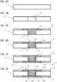
FIGs. 2A to 2F are cross-sectional views showing steps relating to a production method of the circuit board according to an embodiment of the present invention; -
FIG. 3 is a cross-sectional view showing a schematic configuration of the circuit board relating to a modification example of an embodiment of the present invention; -
FIG. 4 is a cross-sectional view showing a schematic configuration of the circuit board relating to a modification example of an embodiment of the present invention; -
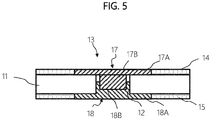
FIG. 5 is a cross-sectional view showing a schematic configuration of the circuit board relating to a modification example of an embodiment of the present invention; -
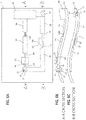
FIG. 6A is a top view showing a schematic configuration of an electronic circuit device according to a second embodiment of the present invention, andFIGs. 6B and 6C are cross-sectional views thereof; -
FIGs. 7A and 7B are cross-sectional views showing a schematic configuration of an example of a conventional circuit board; and -
FIGs. 8A and 8B are cross-sectional views showing a schematic configuration of an example of a conventional circuit board. - There will now be described an embodiment of the present invention, with reference to accompanying drawings. For ease of understanding and visibility enhancement in the figures described below, hatching is omitted in some cases as appropriate, even in the cross-sectional views. Hereinafter, configurations being identical are labeled with the same reference numeral, and they will not be redundantly explained.
- There will be described a
circuit board 1 relating to one embodiment of the present invention. - As shown in
FIG. 1 , thecircuit board 1 of the present embodiment comprises, asubstrate 11, a through-hole 12 provided in the substrate, aconductive part 13 filled in the through-hole 12, afrontside wiring pattern 14 provided on the frontside of thesubstrate 11, and abackside wiring pattern 15 provided on the backside of thesubstrate 11. - The through-
hole 12 is formed through thesubstrate 11 at a desired position, penetrating the frontside to the backside of thesubstrate 11. - The
conductive part 13 comprises a frontside conductive part 17 (a first conductive part 17) filled in the through-hole 12 and a backside conductive part 18 (a second conductive part 18). - The frontside conductive part 17 (the first conductive part 17) covers the opening of the through-hole on the frontside of the
substrate 11 in a manner blocking the opening, further comprising afrontside connection part 17A (afirst connection part 17A) connected to thefrontside wiring pattern 14, and acolumnar part 17B formed continuously from the frontside connection part and provided vertically into the through-hole 12. The diameter of thecolumnar part 17B is smaller than the inner diameter of the through-hole 12. The frontside conductive part 17 (the first conductive part 17) and thefrontside wiring pattern 14 may be formed as a single piece. - The backside conductive part 18 (the second conductive part 18) covers the opening of the through-hole on the backside of the
substrate 11 in a manner blocking the opening, further comprising abackside connection part 18A (asecond connection part 18A) connected to thebackside wiring pattern 15, and ashape 18B (hereinafter, referred to as aconcave part 18B) bonded to thecolumnar part 17B within the through-hole 12 so as to fill the gap between thecolumnar part 17B and the inner surface of the through-hole 12. The backside conductive part 18 (the second conductive part 18) and thebackside wiring pattern 15 may be formed as a single piece. - Both of the frontside
conductive part 17 and the backsideconductive part 18 comprise conductive particles being sintered. - As described so far, in the present embodiment, within the through-hole, the diameter of the
columnar part 17B of the firstconductive part 17 is smaller than the inner diameter of the through-hole and the secondconductive part 18 has the shape to fill the gap between the inner surface of the through-hole 12 and thecolumnar part 17B. Therefore, the firstconductive part 17 is bonded to the secondconductive part 18, on both the circumference and the bottom of thecolumnar part 17B, and thus the area of joint is large. In addition, both the frontsideconductive part 17 and the backsideconductive part 18 comprise conductive particles being sintered, and this allows rigid bonding between the boundaries of the firstconductive part 17 and the secondconductive part 18 when sintering is performed. With this configuration, even when tension is applied to the through-hole and in proximity thereof, due to expansion and contraction of the substrate or a bend therein, thermal shock or environmental testing, and so on, the likelihood of through-hole disconnection and/or increase of resistance can be reduced. - According to the production method as described below, the first
conductive part 17 in the center of the through-hole 12 is formed prior to forming the secondconductive part 18 that fills the gap around theconductive part 17, whereby the width of the gap to be filled with the secondconductive part 18 can be made smaller relative to the diameter of the firstconductive part 17. Therefore, contraction of the secondconductive part 18 upon sintering can be reduced, whereby gaps generated in the entireconductive part 13 may be minimized with respect to the through-hole 12. Since the contraction of the secondconductive part 18 is small, this may avoid deformation such as dents on the bottom of the secondconductive part 18, due to the contraction. - Naming of the frontside
conductive part 17 and the backsideconductive part 18, using the terms "frontside" and "backside", is defined just for the sake of convenience, and the frontsideconductive part 17 may be arranged on the lower side, and the backsideconductive part 18 may be arranged on the upper side. - It is desirable that neither the first
conductive part 17 nor the secondconductive part 18 contain resin. The firstconductive part 17 may be obtained by sintering conductive nanoparticles having a diameter smaller than 1 µm, or obtained by sintering mixture of the conductive nanoparticles having a diameter smaller than 1 µm and conductive microparticles having a diameter equal to or greater than 1 µm and smaller than 1 mm. The secondconductive part 18 may also be obtained by sintering conductive nanoparticles having a diameter smaller than 1 µm, or obtained by sintering mixture of the conductive nanoparticles having a diameter smaller than 1 µm and conductive microparticles having a diameter equal to or greater than 1 µm and smaller than 1 mm. It is to be noted that the diameter of the particle referred to here indicates an average diameter of the particle. - In any of the above cases, an average diameter of the conductive particles of the first
conductive part 17 before sintering is preferably equivalent to or smaller than the average diameter of the conductive particles of the second conductive part before sintering, because the smaller is the diameter, the larger contraction is induced when sintering is performed. - Around the through-hole on at least one surface of the
substrate 11, there may be mountedwiring pattern wiring patter 14 being connected to the firstconductive part 17 and thewiring pattern 15 being connected to the secondconductive part 18. Thewiring patterns substrate 11 may be flexible. Since thewiring patterns substrate 11 is flexible. - Next, with reference to
FIG. 2 , there will be described a method for producing thecircuit board 1 that is formed as described above. - At a predetermined position on the
substrate 11 as shown inFIG. 2A , the through-hole 12 is formed passing through the substrate as shown inFIG. 2B , according to any method, for example, stamping, laser processing, and so on. - Subsequently, as shown in
FIG. 2C , the first conductive paste obtained by dispersing conductive particles in a solvent is prepared, the first conductive paste is applied to a predetermined region in proximity to the edge of the through-hole 12, using a method such as screen printing, from the frontside of thesubstrate 11, along with filling the through-hole 12. - In the present embodiment, preferably, nanoparticles having a diameter smaller than 1 µm may be employed as the conductive particles for the first conductive paste, so as to cause volume contraction when sintering is performed. However, microparticles having a diameter between or equal to 1 µm and 100 µm may be contained partially. Those microparticles thus contained may reduce the volume contraction, but this may allow sintering of the conductive particles easily with keeping the shape of the first conductive paste, and this facilitates maintaining of the columnar shape. By way of example, the proportion of nanoparticles having a diameter smaller than 1 µm in the conductive particles contained in the first conductive paste, is preferably between or equal to 40 wt% and 100wt%, more preferably between or equal to 70 wt% and 100 wt%, and much more preferably between or equal to 75 wt% and 100 wt%.
- Furthermore, if the proportion of the conductive particles in the first conductive paste is too low, it becomes harder to sinter the conductive particles with keeping the shape of the first conductive paste, and this makes forming of the
columnar part 17B more difficult. Therefore, the proportion of the conductive particles in the first conductive paste is preferably between or equal to 50 wt% and 98 wt%, more preferably between or equal to 60 wt% and 95 wt%, and much more preferably between or equal to 80 wt% and 95 wt%. - The conductive paste may contain, in addition to the solvent and the conductive particles, a dispersant such as polyvinylpyrrolidone, resin, and so on. However, it is preferable not to contain the resin (e.g., epoxy resin, silicone resin, and urethane resin), because if any resin remains upon sintering, this may reduce the volume contraction. Since a large amount of dispersant may also reduce the volume contraction, the dispersant should be added in small concentrations to a degree that may not hamper the dispersion.
- As for the solvent, too low viscosity of the solvent may cause failure in keeping the shape when filled in the through-
hole 12, and thus it is preferable to use the solvent with viscosity that enables keeping of the shape. - Specific examples of the substrate, the conductive particles, and the solvent will be described later.
- Simultaneously with filling the through-hole 12b with the first conductive paste, or continuously therefrom, the first conductive paste is applied to the surface of the
substrate 11, in the shape of thefrontside wiring pattern 14 according to a method such as printing. - Then, as shown in
FIG. 2D , an electromagnetic wave or heat is applied to the first conductive paste, thereby sintering the conductive particles within the conductive paste. A wavelength and other conditions in performing the sintering using the electromagnetic wave will be described later. - With this sintering, the solvent contained in the conductive paste evaporates and the conductive particles are sintered (fused), and then, this causes volume contraction in the conductive paste. Therefore, the conductive paste applied to the proximity of the edge of the through-hole forms the
frontside connection part 17A by sintering, and simultaneously, this sintering causes the volume contraction in the conductive paste filled in the through-hole 12 toward the center, separating from the inner surface of the through-hole 12, thereby forming thecolumnar part 17B. In other words, the conductive paste contracts by sintering, and the frontsideconductive part 17 with a T-shaped cross section is formed, comprising thefrontside connection part 17A and thecolumnar part 17B. Then, thegap 19 is generated between the inner surface of the through-hole 12 and thecolumnar part 17B. - By way of example, the through-
hole 12 having a diameter of 300 µm was formed through thesubstrate 11 having a thickness of 100 µm, the through-hole was filled with the conductive paste where 85 wt% silver particles having an average diameter of 50 nm were dispersed in an organic solvent, and sintering was performed at 160°C to 200°C. Then, the diameter was contracted approximately by 10%, causing thegap 19. - Furthermore, the first conductive paste in the through-
hole 12 is also applied to the surface of thesubstrate 11, and then sintered to form thefrontside wiring pattern 14. - Next, the second conductive paste is prepared to form the second
conductive part 18. The proportion of nanoparticles having a diameter smaller than 1 µm in the conductive particles contained in the secondconductive paste 18, is preferably between or equal to 0 wt% and 100wt%, more preferably between or equal to 0 wt% and 90 wt%, and much more preferably between or equal to 0 wt% and 80 wt%. - The proportion of the conductive particles in the second conductive paste is preferably between or equal to 50 wt% and 98 wt%, more preferably between or equal to 60 wt% and 95 wt%, and much more preferably between or equal to 80 wt% and 95 wt%.
- Less volume contraction is required in the second conductive paste relative to the volume contraction in the first conductive paste used for the frontside
conductive part 17. Therefore, for example, the proportion of conductive microparticles can be higher than the conductive paste used for the frontsideconductive part 17. - In the example here, the conductive paste used as the second conductive paste is the same as the first conductive paste.
- As shown in
FIG. 2E , the second conductive paste is applied to a predetermined region in proximity to the edge of the through-hole 12, using a method such as screen printing, from the backside of thesubstrate 11, along with filling thegap 19 between the inner surface of the through-hole 12 and thecolumnar part 17B. - As shown in
FIG. 2E , simultaneously with or continuously from the previous step, the conductive paste serving as thebackside wiring pattern 15 is also applied to the backside of thesubstrate 11. - Subsequently, as shown in
FIG. 2F , an electromagnetic wave or heat is applied to the second conductive paste, thereby sintering the conductive paste. Then, the conductive paste applied to the proximity of the edge of the through-hole forms thebackside connection part 18A, and simultaneously, the conductive paste filled in the gap between the inner surface of the through-hole 12 and thecolumnar part 17B is sintered to form theconcave part 18B. Volume contraction occurs in theconcave part 18B toward the center of the through-hole 12, whereby the concave part is rigidly bonded to thecolumnar part 17B. In other words, the conductive paste contracts by sintering, and the backsideconductive part 18 is formed, comprising thebackside connection part 18A and theconcave part 18B. - Upon heating the second conductive paste within the through-
hole 12, heat is conducted also to the firstconductive part 17 with which the second conductive paste comes into contact, and the firstconductive part 17 is heated for the second time. Therefore, the conductive particles in the firstconductive part 17 and the conductive particles in the second conductive paste are sintered together. According to this sintering, the joint surfaces between the firstconductive part 17 and the secondconductive part 18 are substantially integrated. - According to the process above, there are formed the frontside
conductive part 17 and the backsideconductive part 18 within the through-hole 12, obtained by sintering the conductive paste. - Furthermore, the second conductive paste applied to the surface of the
substrate 11 in the shape of the wiring pattern is also sintered simultaneously with or continuously from heating the second conductive paste within the through-hole, thereby forming thebackside wiring pattern 15. - Preferably, a range for applying the conductive paste to form the
frontside connection part 17A and thebackside connection part 18A should be set appropriately, considering a relationship with other electronic components to be mounted on thesubstrate 11 and wiring patterns. When a bend or expansion/contraction occurs in thesubstrate 11, tension is likely to be concentrated on the edge of the through-hole 12. Therefore, it is preferable to determine the application range of the conductive paste to be applied to form thefrontside connection part 17A and thebackside connection part 18A, in a manner that contact positions respectively between thefrontside connection part 17A and the frontside wiring pattern, and between thebackside connection part 18A and the backside wiring pattern, should be set to the points less affected by the tension concentrated to the through-hole 12. - As described above, according to the present embodiment, a material with large volume contraction is used as the first conductive paste forming the first conductive part, and thus generated gap is filled with the second conductive paste from the backside and then sintered. Accordingly, the area of joint between the frontside conductive part and the backside conductive part is large, excellent in conductivity and heat dispersion, and therefore, this reduces a likelihood of so-called through-hole disconnection, and connection reliability on both sides of the substrate can be enhanced.
- Filling the through-hole with the conductive paste, and application of the conductive paste to form the wiring pattern can be performed simultaneously, thereby reducing the number of production steps. When application of the conductive paste is performed by screen printing, an air vent can be provided easily, and this produces an advantage that facilitates filling of the conductive paste into the entire through-hole.
- The wiring pattern may be formed simultaneously with forming the through-hole, or it may be formed prior to or after forming the through-hole.
- Any material may be used for the
substrate 11, as far as the material is capable of supporting the first and the secondconductive parts wiring patterns conductive parts substrate 11. As shown inFIG. 6 , thesubstrate 11 may have the curved shape. - As a material of the conductive particle, at least one of the conductive metals such as Ag, Cu, Au, Pt, Ni, and Pd may be employed.
- As the solvent where the conductive particles are dispersed, organic solvents, such as amine, alcohol, ether, aromatic compounds, ketone, and nitrile, and water may be employed.
- The
substrate 11 can be formed with a thickness from about 100 nm to 3 mm. The diameter of the through-hole 12 may be between or equal to 5 µm and 1 mm. Electrical resistivity of theconductive part 13 within the through-hole is preferably 10-4 Ω·cm or less, and in particular, low resistance in the order of 10-6 Ω·cm is desirable. The electrical resistivity of thewiring patterns - Specifically, at least one of the following methods may be employed for sintering the conductive paste; sintering by irradiation of electromagnetic waves such as light, and sintering according to a method other than the irradiation of electromagnetic waves. When the
substrate 11 has optical transparency, any of the upper surface and the lower surface of thesubstrate 11 may be irradiated with light. When thesubstrate 11 does not have optical transparency, the substrate is irradiated with light from the upper surface. - When the conductive paste particles are sintered, the conductive particles are melted at a temperature lower than a melting point of bulk material constituting the particles, integrated (fused) with neighboring conductive particles, and then sintered. When the conductive paste particles are sintered by electromagnetic wave irradiation, light or electromagnetic wave being radiated may have any wavelength, such as ultraviolet, visible, and infrared light, but a wavelength absorbable by the conductive particles should be selected for use. When materials such as Ag, Cu, and Au are employed for the conductive particle, the light in the range from 400 to 1064 nm can be used as the electromagnetic wave, for instance. In addition, light beams collected into an irradiation diameter smaller than or equivalent to the through-
hole 12 may be employed, preventing a part of thesubstrate 11 to which the light beams are not applied from being heated. Therefore, even when a resin substrate is used, thesubstrate 11 is hardly damaged, and transparency of thetransparent substrate 11 can be maintained. In addition, by scanning the light beams, thewiring patterns - There has been described an example that the
wiring patterns - There will now be described modification examples.
- The circuit boards as shown in
FIG. 3 and FIG. 4 have the through-hole 12 in tapered shape, formed in thesubstrate 11. The through-hole 12 passing through the substrate is made with the use of laser or a similar method, whereby this tapered-shape through-hole can be formed. - As indicated by the circuit board shown in
FIG. 5 , the backside conductive part does not necessarily fill the gap generated between the inner surface of the through-hole 12 and thecolumnar part 17B. - By way of example, even when the backside conductive part fills the gap to a level from a half to a quarter of the thickness of the
substrate 11, the area of joint between the frontside conductive part and the backside conductive part can be provided, thus reducing the likelihood of the through-hole disconnection. - In the modification examples, since the configuration and effects of the circuit board other than the description above, which are shown in
FIGs. 3 to 5 , are the same as the aforementioned embodiment, redundant descriptions will not be provided. - With reference to
FIGs. 6A to 6C , there will now be described an electronic circuit device configured with thecircuit board 1 that relates to the aforementioned embodiment. This electronic circuit device has a configuration whereelectronic components 30 are mounted on both sides of thecircuit board 11. In addition, aresistance 140 is formed on the upper surface of thecircuit board 11. - Any element may be used as the
electronic component 30, and by way of example, a light emitting element (LED, LD), a light receiving element, an integrated circuit, a display element (such as a liquid crystal display and an EL display), a vehicle-mounted electronic component, or the like, may be employed. Thewiring patterns electronic components 30 is connected in a desired circuit pattern, such as in series and in parallel. - The through-
hole 12 and theconductive part 13 are provided on the positions allowing both of the wiring patterns to be connected. - A flexible material may be used for the
substrate 11, and a transparent material can also be used. - Accordingly, this electronic circuit device may configure a vehicle-use electronic circuit device equipped with vehicle-use electronic components, and may also be applied to electronic devices such as communication equipment, gaming equipment, and OA equipment. By way of example, this electronic circuit device may serve as a device such as an instrument panel of a vehicle, and a monitor of a gaming machine. Since the substrate is allowed to bend, it is applicable to a wearable (body wearable) electronic device (such as glasses, a watch, a display, and medical equipment), and a curved display.
Claims (19)
- A circuit board comprising,a substrate with a through-hole,a first conductive part covering an opening of the through-hole on one surface of the substrate in a manner blocking the opening, having a portion inserted into the through-hole from the one surface, anda second conductive part covering a second opening of the through-hole on the other surface of the substrate in a manner blocking the second opening, having a portion inserted into the through-hole from the other surface, wherein,the portion of the first conductive part inserted in the through-hole has a columnar shape, forming a columnar portion having a diameter smaller than the through-hole,the portion of the second conductive part inserted in the through-hole has a shape that fills a gap between the columnar portion of the first conductive part and an inner surface of the through-hole, andboth of the first conductive part and the second conductive part comprise conductive particles being sintered.
- The circuit board according to claim 1, wherein,
neither the first conductive part nor the second conductive part contains resin. - The circuit board according to either of claims 1 and 2, wherein,
the first conductive part is obtained by sintering conductive nanoparticles having a diameter smaller than 1 µm. - The circuit board according to either of claims 1 and 2, wherein,
the first conductive part is obtained by sintering mixture of the conductive nanoparticles having a diameter smaller than 1 µm and conductive microparticles having a diameter equal to or greater than 1 µm and smaller than 1 mm. - The circuit board according to either of claims 3 and 4, wherein,
the second conductive part is obtained by sintering conductive nanoparticles having the diameter smaller than 1 µm. - The circuit board according to either of claims 3 and 4, wherein,
the second conductive part is obtained by sintering mixture of the conductive nanoparticles having the diameter smaller than 1 µm and conductive microparticles having the diameter equal to or greater than 1 µm and smaller than 1 mm. - The circuit board according to any one of claims 3 to 6 wherein,
an average diameter of the conductive particles of the first conductive part before sintering is equivalent to or smaller than the average diameter of the conductive particles of the second conductive part before sintering. - The circuit board according to any one of claims 1 to 7 wherein,
a wiring pattern is mounted being connected to the first conductive part or to the second conductive part, around the through-hole on at least one of the surfaces of the substrate, and the wiring pattern comprises conductive particles being sintered. - The circuit board according to any one of claims 1 to 8 wherein,
the substrate is flexible. - An electronic circuit device comprising a circuit board provided with wiring patterns, and electronic components mounted on at least one side of the circuit board, wherein,the circuit board comprising,a substrate with a through-hole,a first conductive part covering an opening of the through-hole on one surface of the substrate in a manner blocking the opening, having a portion inserted into the through-hole from the one surface, anda second conductive part covering a second opening of the through-hole on the other surface of the substrate in a manner blocking the second opening, having a portion inserted into the through-hole from the other surface, wherein,the portion of the first conductive part inserted in the through-hole has a columnar shape, forming a columnar portion having a diameter smaller than the through-hole,the portion of the second conductive part inserted in the through-hole has a shape that fills a gap between the columnar portion of the first conductive part and an inner surface of the through-hole, andboth of the first and the second conductive parts comprise conductive particles being sintered.
- A production method of a circuit board, comprising,a first step of filling a through-hole with a first conductive paste, from one surface of a substrate having the through-hole, the first conductive paste obtained by dispersing conductive particles in a solvent,a second step of forming a first conductive part having a portion inserted in the through-hole, the diameter of the portion being smaller than the through-hole, by heating the first conductive paste for contracting the first conductive paste along with sintering the conductive particles therein,a third step of filling a gap between an inner surface of the through-hole and the first conductive part, with a second conductive paste obtained by dispersing conductive particles in a solvent, from the other surface of the substrate, anda fourth step of forming a second conductive part filling the gap between the inner surface of the through-hole and the first conductive part, by heating the second conductive paste for contracting the second conductive paste along with sintering the conductive particles therein.
- The production method of the circuit board, according to claim 11, wherein,
a proportion of the conductive particles in the first conductive paste is between or equal to 50 wt% and 98 wt%. - The production method of the circuit board, according to either of claims 11 to 12, wherein,
the proportion of nanoparticles having a diameter smaller than 1 µm in the conductive particles contained in the first conductive paste, is equal to or more than 40 wt%. - The production method of the circuit board, according to any one of claims 11 to 13, wherein,
an average diameter of the conductive particles contained in the first conductive paste is equivalent to or smaller than the average diameter of the conductive particles contained in the second conductive paste. - The production method of the circuit board, according to any one of claims 11 to 14, wherein,
in the second step and the fourth step, the first conductive paste and the second conductive paste are heated by irradiation of electromagnetic waves. - The production method of the circuit board, according to any one of claims 11 to 15, wherein,
in the first step, the first conductive paste is applied to the one surfaces of the substrate, in the shape of a wiring pattern, simultaneously with filling the through-hole with the first conductive paste. - The production method of the circuit board, according to claim 16, wherein,
in the second step, the first conductive paste in the shape of the wiring pattern is heated, simultaneously with or continuously from heating the first conductive paste within the through-hole. - The production method of the circuit board, according to any one of claims 11 to 17, wherein,
in the third step, the second conductive paste is applied to other surface of the substrate, in the shape of a wiring pattern, simultaneously with filling the through-hole with the second conductive paste. - The production method of the circuit board, according to claim 18, wherein,
in the fourth step, the second conductive paste in the shape of the wiring pattern is heated, simultaneously with or continuously from heating the second conductive paste within the through-hole.
Applications Claiming Priority (1)
| Application Number | Priority Date | Filing Date | Title |
|---|---|---|---|
| JP2018042331A JP7075785B2 (en) | 2018-03-08 | 2018-03-08 | Circuit boards, electronic circuit devices, and methods for manufacturing circuit boards |
Publications (2)
| Publication Number | Publication Date |
|---|---|
| EP3537854A1 true EP3537854A1 (en) | 2019-09-11 |
| EP3537854B1 EP3537854B1 (en) | 2022-02-09 |
Family
ID=65724179
Family Applications (1)
| Application Number | Title | Priority Date | Filing Date |
|---|---|---|---|
| EP19161025.2A Active EP3537854B1 (en) | 2018-03-08 | 2019-03-06 | Production method of circuit board |
Country Status (4)
| Country | Link |
|---|---|
| US (1) | US10932373B2 (en) |
| EP (1) | EP3537854B1 (en) |
| JP (1) | JP7075785B2 (en) |
| CN (1) | CN110248466B (en) |
Cited By (1)
| Publication number | Priority date | Publication date | Assignee | Title |
|---|---|---|---|---|
| CN113275567A (en) * | 2021-04-30 | 2021-08-20 | 广东工业大学 | Laser sintering forming method |
Families Citing this family (12)
| Publication number | Priority date | Publication date | Assignee | Title |
|---|---|---|---|---|
| WO2020027022A1 (en) * | 2018-07-31 | 2020-02-06 | 京セラ株式会社 | Printed-wiring board and method of manufacturing printed-wiring board |
| JP2021056383A (en) | 2019-09-30 | 2021-04-08 | 日東電工株式会社 | Gap filling method, gap filling structure, and method of manufacturing the same |
| JP2021125520A (en) * | 2020-02-04 | 2021-08-30 | 矢崎総業株式会社 | Printed circuit board and manufacturing method thereof |
| JP2021125521A (en) * | 2020-02-04 | 2021-08-30 | 矢崎総業株式会社 | Printed wiring board, printed circuit board, and manufacturing method of printed wiring board |
| CN217086601U (en) * | 2020-12-28 | 2022-07-29 | 中国科学院苏州纳米技术与纳米仿生研究所 | Intercommunicating electrode structure |
| CN114695664A (en) * | 2020-12-28 | 2022-07-01 | 中国科学院苏州纳米技术与纳米仿生研究所 | Flexible photoelectric device and manufacturing method |
| CN114759018B (en) * | 2020-12-28 | 2025-10-03 | 中国科学院苏州纳米技术与纳米仿生研究所 | Flexible optoelectronic device assembly and manufacturing method thereof |
| JP7422336B2 (en) * | 2021-07-28 | 2024-01-26 | 日亜化学工業株式会社 | Planar light source |
| US12512414B2 (en) * | 2021-10-11 | 2025-12-30 | Intel Corporation | Vertical interconnect design for improved electrical performance |
| US20230369284A1 (en) * | 2022-05-12 | 2023-11-16 | Pac Tech - Packaging Technologies Gmbh | Chip arrangement and method for forming a sintered contact connection |
| CN224460160U (en) * | 2023-02-16 | 2026-07-03 | 株式会社村田制作所 | Multilayer substrate and electronic device |
| CN118073438A (en) * | 2024-02-07 | 2024-05-24 | 南京航空航天大学 | A method for preparing a photovoltaic cell electrode |
Citations (5)
| Publication number | Priority date | Publication date | Assignee | Title |
|---|---|---|---|---|
| JP4012022B2 (en) | 2002-09-06 | 2007-11-21 | 株式会社フジクラ | Multilayer wiring substrate, base material for multilayer wiring substrate, and manufacturing method thereof |
| US20090274834A1 (en) * | 2008-05-01 | 2009-11-05 | Xerox Corporation | Bimetallic nanoparticles for conductive ink applications |
| WO2016170900A1 (en) * | 2015-04-24 | 2016-10-27 | スタンレー電気株式会社 | Resistor production method, resistor, and electronic device |
| WO2016170902A1 (en) * | 2015-04-24 | 2016-10-27 | スタンレー電気株式会社 | Electronic device production method, electronic device, circuit board production method, and circuit board |
| US20170238425A1 (en) * | 2016-02-12 | 2017-08-17 | Tyco Electronics Corporation | Method of Fabricating Highly Conductive Features with Silver Nanoparticle Ink at Low Temperature |
Family Cites Families (15)
| Publication number | Priority date | Publication date | Assignee | Title |
|---|---|---|---|---|
| JP2794960B2 (en) * | 1991-02-19 | 1998-09-10 | 松下電器産業株式会社 | Sintered conductor wiring board and its manufacturing method |
| JP2807976B2 (en) * | 1995-02-14 | 1998-10-08 | ニッコー株式会社 | Manufacturing method of through hole filled with conductor |
| JP3867523B2 (en) * | 2000-12-26 | 2007-01-10 | 株式会社デンソー | Printed circuit board and manufacturing method thereof |
| SE0100134D0 (en) * | 2001-01-15 | 2001-01-15 | Abb Ab | Industrial robot |
| JP3900248B2 (en) * | 2001-03-30 | 2007-04-04 | ハリマ化成株式会社 | Multilayer wiring board and method for forming the same |
| JP2002353615A (en) * | 2001-05-22 | 2002-12-06 | Shin Etsu Polymer Co Ltd | Method for conducting between wiring patterns on both sides of flexible printed wiring board and flexible printed wiring board formed using the method |
| EP1672971B1 (en) * | 2003-09-12 | 2017-11-01 | National Institute of Advanced Industrial Science and Technology | Method for manufacturing a substrate |
| US8063315B2 (en) * | 2005-10-06 | 2011-11-22 | Endicott Interconnect Technologies, Inc. | Circuitized substrate with conductive paste, electrical assembly including said circuitized substrate and method of making said substrate |
| TW200842900A (en) * | 2007-04-27 | 2008-11-01 | Du Pont | Electrically conductive composition for via-holes |
| EP2157842B1 (en) * | 2007-05-17 | 2018-03-14 | Fujikura, Ltd. | Laminated wiring board and method for manufacturing the same |
| WO2009090748A1 (en) * | 2008-01-17 | 2009-07-23 | Applied Nanoparticle Laboratory Corporation | Silver composite nanoparticle and process and apparatus for producing the same |
| JP2009177011A (en) * | 2008-01-25 | 2009-08-06 | Ferrotec Ceramics Corp | Conductive member and parts and apparatus using the same |
| EP2475235B1 (en) * | 2009-11-10 | 2019-08-21 | Murata Manufacturing Co., Ltd. | Multilayer board and manufacturing method thereof |
| US8891245B2 (en) * | 2011-09-30 | 2014-11-18 | Ibiden Co., Ltd. | Printed wiring board |
| JP6058321B2 (en) * | 2012-09-04 | 2017-01-11 | 日本特殊陶業株式会社 | Wiring board manufacturing method |
-
2018
- 2018-03-08 JP JP2018042331A patent/JP7075785B2/en active Active
-
2019
- 2019-02-13 CN CN201910112398.0A patent/CN110248466B/en active Active
- 2019-03-06 EP EP19161025.2A patent/EP3537854B1/en active Active
- 2019-03-08 US US16/296,547 patent/US10932373B2/en active Active
Patent Citations (6)
| Publication number | Priority date | Publication date | Assignee | Title |
|---|---|---|---|---|
| JP4012022B2 (en) | 2002-09-06 | 2007-11-21 | 株式会社フジクラ | Multilayer wiring substrate, base material for multilayer wiring substrate, and manufacturing method thereof |
| US20090274834A1 (en) * | 2008-05-01 | 2009-11-05 | Xerox Corporation | Bimetallic nanoparticles for conductive ink applications |
| WO2016170900A1 (en) * | 2015-04-24 | 2016-10-27 | スタンレー電気株式会社 | Resistor production method, resistor, and electronic device |
| WO2016170902A1 (en) * | 2015-04-24 | 2016-10-27 | スタンレー電気株式会社 | Electronic device production method, electronic device, circuit board production method, and circuit board |
| US20180158580A1 (en) * | 2015-04-24 | 2018-06-07 | Stanley Electric Co., Ltd. | Resistor production method, resistor, and electronic device |
| US20170238425A1 (en) * | 2016-02-12 | 2017-08-17 | Tyco Electronics Corporation | Method of Fabricating Highly Conductive Features with Silver Nanoparticle Ink at Low Temperature |
Cited By (1)
| Publication number | Priority date | Publication date | Assignee | Title |
|---|---|---|---|---|
| CN113275567A (en) * | 2021-04-30 | 2021-08-20 | 广东工业大学 | Laser sintering forming method |
Also Published As
| Publication number | Publication date |
|---|---|
| JP7075785B2 (en) | 2022-05-26 |
| EP3537854B1 (en) | 2022-02-09 |
| JP2019160885A (en) | 2019-09-19 |
| US10932373B2 (en) | 2021-02-23 |
| US20190281705A1 (en) | 2019-09-12 |
| CN110248466A (en) | 2019-09-17 |
| CN110248466B (en) | 2024-06-07 |
Similar Documents
| Publication | Publication Date | Title |
|---|---|---|
| US10932373B2 (en) | Circuit board, electronic circuit device, and production method of circuit board | |
| US8525038B2 (en) | Flex-rigid wiring board and method of manufacturing the same | |
| US8925194B2 (en) | Flex-rigid wiring board and method of manufacturing the same | |
| KR100939426B1 (en) | Flex rigid wiring board | |
| US10085349B2 (en) | Method for producing electronic device, and electronic device | |
| EP2187720A1 (en) | Flexible wiring board, and its manufacturing method | |
| JP6491032B2 (en) | Manufacturing method of resistor and resistor | |
| US10383214B2 (en) | Electronic device, method for producing same, and circuit substrate | |
| KR100908975B1 (en) | Flex Rigid Wiring Boards and Manufacturing Method Thereof | |
| CN103918356A (en) | Method for manufacturing component-embedded substrate and component-embedded substrate manufactured using the method | |
| CN104041196A (en) | Double sided printed circuit board and method for manufacturing same | |
| US10912201B2 (en) | Electronic device and production method thereof | |
| JP6771346B2 (en) | Manufacturing method of electronic device and electronic device | |
| JP7137354B2 (en) | Multilayer circuit board and manufacturing method thereof | |
| JP2016207904A (en) | Circuit board manufacturing method, electronic device manufacturing method, and electronic device | |
| KR100942626B1 (en) | Flex-rigid wiring board and method of manufacturing the same | |
| WO2011024469A1 (en) | Substrate producing method and resin substrate |
Legal Events
| Date | Code | Title | Description |
|---|---|---|---|
| PUAI | Public reference made under article 153(3) epc to a published international application that has entered the european phase |
Free format text: ORIGINAL CODE: 0009012 |
|
| STAA | Information on the status of an ep patent application or granted ep patent |
Free format text: STATUS: THE APPLICATION HAS BEEN PUBLISHED |
|
| AK | Designated contracting states |
Kind code of ref document: A1 Designated state(s): AL AT BE BG CH CY CZ DE DK EE ES FI FR GB GR HR HU IE IS IT LI LT LU LV MC MK MT NL NO PL PT RO RS SE SI SK SM TR |
|
| AX | Request for extension of the european patent |
Extension state: BA ME |
|
| STAA | Information on the status of an ep patent application or granted ep patent |
Free format text: STATUS: REQUEST FOR EXAMINATION WAS MADE |
|
| 17P | Request for examination filed |
Effective date: 20200311 |
|
| RBV | Designated contracting states (corrected) |
Designated state(s): AL AT BE BG CH CY CZ DE DK EE ES FI FR GB GR HR HU IE IS IT LI LT LU LV MC MK MT NL NO PL PT RO RS SE SI SK SM TR |
|
| RIC1 | Information provided on ipc code assigned before grant |
Ipc: H05K 1/03 20060101ALN20210921BHEP Ipc: H05K 3/40 20060101ALI20210921BHEP Ipc: H05K 3/12 20060101ALI20210921BHEP Ipc: H05K 1/09 20060101AFI20210921BHEP |
|
| RIC1 | Information provided on ipc code assigned before grant |
Ipc: H05K 1/03 20060101ALN20210927BHEP Ipc: H05K 3/40 20060101ALI20210927BHEP Ipc: H05K 3/12 20060101ALI20210927BHEP Ipc: H05K 1/09 20060101AFI20210927BHEP |
|
| RIC1 | Information provided on ipc code assigned before grant |
Ipc: H05K 1/03 20060101ALN20211008BHEP Ipc: H05K 3/40 20060101ALI20211008BHEP Ipc: H05K 3/12 20060101ALI20211008BHEP Ipc: H05K 1/09 20060101AFI20211008BHEP |
|
| GRAP | Despatch of communication of intention to grant a patent |
Free format text: ORIGINAL CODE: EPIDOSNIGR1 |
|
| STAA | Information on the status of an ep patent application or granted ep patent |
Free format text: STATUS: GRANT OF PATENT IS INTENDED |
|
| INTG | Intention to grant announced |
Effective date: 20211122 |
|
| GRAS | Grant fee paid |
Free format text: ORIGINAL CODE: EPIDOSNIGR3 |
|
| GRAA | (expected) grant |
Free format text: ORIGINAL CODE: 0009210 |
|
| STAA | Information on the status of an ep patent application or granted ep patent |
Free format text: STATUS: THE PATENT HAS BEEN GRANTED |
|
| AK | Designated contracting states |
Kind code of ref document: B1 Designated state(s): AL AT BE BG CH CY CZ DE DK EE ES FI FR GB GR HR HU IE IS IT LI LT LU LV MC MK MT NL NO PL PT RO RS SE SI SK SM TR |
|
| REG | Reference to a national code |
Ref country code: GB Ref legal event code: FG4D |
|
| REG | Reference to a national code |
Ref country code: CH Ref legal event code: EP Ref country code: AT Ref legal event code: REF Ref document number: 1468298 Country of ref document: AT Kind code of ref document: T Effective date: 20220215 |
|
| REG | Reference to a national code |
Ref country code: IE Ref legal event code: FG4D |
|
| REG | Reference to a national code |
Ref country code: DE Ref legal event code: R096 Ref document number: 602019011385 Country of ref document: DE |
|
| REG | Reference to a national code |
Ref country code: LT Ref legal event code: MG9D |
|
| REG | Reference to a national code |
Ref country code: NL Ref legal event code: MP Effective date: 20220209 |
|
| REG | Reference to a national code |
Ref country code: AT Ref legal event code: MK05 Ref document number: 1468298 Country of ref document: AT Kind code of ref document: T Effective date: 20220209 |
|
| PG25 | Lapsed in a contracting state [announced via postgrant information from national office to epo] |
Ref country code: SE Free format text: LAPSE BECAUSE OF FAILURE TO SUBMIT A TRANSLATION OF THE DESCRIPTION OR TO PAY THE FEE WITHIN THE PRESCRIBED TIME-LIMIT Effective date: 20220209 Ref country code: RS Free format text: LAPSE BECAUSE OF FAILURE TO SUBMIT A TRANSLATION OF THE DESCRIPTION OR TO PAY THE FEE WITHIN THE PRESCRIBED TIME-LIMIT Effective date: 20220209 Ref country code: PT Free format text: LAPSE BECAUSE OF FAILURE TO SUBMIT A TRANSLATION OF THE DESCRIPTION OR TO PAY THE FEE WITHIN THE PRESCRIBED TIME-LIMIT Effective date: 20220609 Ref country code: NO Free format text: LAPSE BECAUSE OF FAILURE TO SUBMIT A TRANSLATION OF THE DESCRIPTION OR TO PAY THE FEE WITHIN THE PRESCRIBED TIME-LIMIT Effective date: 20220509 Ref country code: NL Free format text: LAPSE BECAUSE OF FAILURE TO SUBMIT A TRANSLATION OF THE DESCRIPTION OR TO PAY THE FEE WITHIN THE PRESCRIBED TIME-LIMIT Effective date: 20220209 Ref country code: LT Free format text: LAPSE BECAUSE OF FAILURE TO SUBMIT A TRANSLATION OF THE DESCRIPTION OR TO PAY THE FEE WITHIN THE PRESCRIBED TIME-LIMIT Effective date: 20220209 Ref country code: HR Free format text: LAPSE BECAUSE OF FAILURE TO SUBMIT A TRANSLATION OF THE DESCRIPTION OR TO PAY THE FEE WITHIN THE PRESCRIBED TIME-LIMIT Effective date: 20220209 Ref country code: ES Free format text: LAPSE BECAUSE OF FAILURE TO SUBMIT A TRANSLATION OF THE DESCRIPTION OR TO PAY THE FEE WITHIN THE PRESCRIBED TIME-LIMIT Effective date: 20220209 Ref country code: BG Free format text: LAPSE BECAUSE OF FAILURE TO SUBMIT A TRANSLATION OF THE DESCRIPTION OR TO PAY THE FEE WITHIN THE PRESCRIBED TIME-LIMIT Effective date: 20220509 |
|
| PG25 | Lapsed in a contracting state [announced via postgrant information from national office to epo] |
Ref country code: PL Free format text: LAPSE BECAUSE OF FAILURE TO SUBMIT A TRANSLATION OF THE DESCRIPTION OR TO PAY THE FEE WITHIN THE PRESCRIBED TIME-LIMIT Effective date: 20220209 Ref country code: LV Free format text: LAPSE BECAUSE OF FAILURE TO SUBMIT A TRANSLATION OF THE DESCRIPTION OR TO PAY THE FEE WITHIN THE PRESCRIBED TIME-LIMIT Effective date: 20220209 Ref country code: GR Free format text: LAPSE BECAUSE OF FAILURE TO SUBMIT A TRANSLATION OF THE DESCRIPTION OR TO PAY THE FEE WITHIN THE PRESCRIBED TIME-LIMIT Effective date: 20220510 Ref country code: FI Free format text: LAPSE BECAUSE OF FAILURE TO SUBMIT A TRANSLATION OF THE DESCRIPTION OR TO PAY THE FEE WITHIN THE PRESCRIBED TIME-LIMIT Effective date: 20220209 Ref country code: AT Free format text: LAPSE BECAUSE OF FAILURE TO SUBMIT A TRANSLATION OF THE DESCRIPTION OR TO PAY THE FEE WITHIN THE PRESCRIBED TIME-LIMIT Effective date: 20220209 |
|
| PG25 | Lapsed in a contracting state [announced via postgrant information from national office to epo] |
Ref country code: IS Free format text: LAPSE BECAUSE OF FAILURE TO SUBMIT A TRANSLATION OF THE DESCRIPTION OR TO PAY THE FEE WITHIN THE PRESCRIBED TIME-LIMIT Effective date: 20220609 |
|
| PG25 | Lapsed in a contracting state [announced via postgrant information from national office to epo] |
Ref country code: SM Free format text: LAPSE BECAUSE OF FAILURE TO SUBMIT A TRANSLATION OF THE DESCRIPTION OR TO PAY THE FEE WITHIN THE PRESCRIBED TIME-LIMIT Effective date: 20220209 Ref country code: SK Free format text: LAPSE BECAUSE OF FAILURE TO SUBMIT A TRANSLATION OF THE DESCRIPTION OR TO PAY THE FEE WITHIN THE PRESCRIBED TIME-LIMIT Effective date: 20220209 Ref country code: RO Free format text: LAPSE BECAUSE OF FAILURE TO SUBMIT A TRANSLATION OF THE DESCRIPTION OR TO PAY THE FEE WITHIN THE PRESCRIBED TIME-LIMIT Effective date: 20220209 Ref country code: EE Free format text: LAPSE BECAUSE OF FAILURE TO SUBMIT A TRANSLATION OF THE DESCRIPTION OR TO PAY THE FEE WITHIN THE PRESCRIBED TIME-LIMIT Effective date: 20220209 Ref country code: DK Free format text: LAPSE BECAUSE OF FAILURE TO SUBMIT A TRANSLATION OF THE DESCRIPTION OR TO PAY THE FEE WITHIN THE PRESCRIBED TIME-LIMIT Effective date: 20220209 Ref country code: CZ Free format text: LAPSE BECAUSE OF FAILURE TO SUBMIT A TRANSLATION OF THE DESCRIPTION OR TO PAY THE FEE WITHIN THE PRESCRIBED TIME-LIMIT Effective date: 20220209 |
|
| REG | Reference to a national code |
Ref country code: CH Ref legal event code: PL |
|
| REG | Reference to a national code |
Ref country code: DE Ref legal event code: R097 Ref document number: 602019011385 Country of ref document: DE |
|
| PG25 | Lapsed in a contracting state [announced via postgrant information from national office to epo] |
Ref country code: MC Free format text: LAPSE BECAUSE OF FAILURE TO SUBMIT A TRANSLATION OF THE DESCRIPTION OR TO PAY THE FEE WITHIN THE PRESCRIBED TIME-LIMIT Effective date: 20220209 Ref country code: AL Free format text: LAPSE BECAUSE OF FAILURE TO SUBMIT A TRANSLATION OF THE DESCRIPTION OR TO PAY THE FEE WITHIN THE PRESCRIBED TIME-LIMIT Effective date: 20220209 |
|
| REG | Reference to a national code |
Ref country code: BE Ref legal event code: MM Effective date: 20220331 |
|
| PLBE | No opposition filed within time limit |
Free format text: ORIGINAL CODE: 0009261 |
|
| STAA | Information on the status of an ep patent application or granted ep patent |
Free format text: STATUS: NO OPPOSITION FILED WITHIN TIME LIMIT |
|
| 26N | No opposition filed |
Effective date: 20221110 |
|
| PG25 | Lapsed in a contracting state [announced via postgrant information from national office to epo] |
Ref country code: LU Free format text: LAPSE BECAUSE OF NON-PAYMENT OF DUE FEES Effective date: 20220306 Ref country code: LI Free format text: LAPSE BECAUSE OF NON-PAYMENT OF DUE FEES Effective date: 20220331 Ref country code: IE Free format text: LAPSE BECAUSE OF NON-PAYMENT OF DUE FEES Effective date: 20220306 Ref country code: CH Free format text: LAPSE BECAUSE OF NON-PAYMENT OF DUE FEES Effective date: 20220331 |
|
| PG25 | Lapsed in a contracting state [announced via postgrant information from national office to epo] |
Ref country code: SI Free format text: LAPSE BECAUSE OF FAILURE TO SUBMIT A TRANSLATION OF THE DESCRIPTION OR TO PAY THE FEE WITHIN THE PRESCRIBED TIME-LIMIT Effective date: 20220209 Ref country code: BE Free format text: LAPSE BECAUSE OF NON-PAYMENT OF DUE FEES Effective date: 20220331 |
|
| PG25 | Lapsed in a contracting state [announced via postgrant information from national office to epo] |
Ref country code: IT Free format text: LAPSE BECAUSE OF FAILURE TO SUBMIT A TRANSLATION OF THE DESCRIPTION OR TO PAY THE FEE WITHIN THE PRESCRIBED TIME-LIMIT Effective date: 20220209 |
|
| PG25 | Lapsed in a contracting state [announced via postgrant information from national office to epo] |
Ref country code: MK Free format text: LAPSE BECAUSE OF FAILURE TO SUBMIT A TRANSLATION OF THE DESCRIPTION OR TO PAY THE FEE WITHIN THE PRESCRIBED TIME-LIMIT Effective date: 20220209 Ref country code: CY Free format text: LAPSE BECAUSE OF FAILURE TO SUBMIT A TRANSLATION OF THE DESCRIPTION OR TO PAY THE FEE WITHIN THE PRESCRIBED TIME-LIMIT Effective date: 20220209 |
|
| PG25 | Lapsed in a contracting state [announced via postgrant information from national office to epo] |
Ref country code: HU Free format text: LAPSE BECAUSE OF FAILURE TO SUBMIT A TRANSLATION OF THE DESCRIPTION OR TO PAY THE FEE WITHIN THE PRESCRIBED TIME-LIMIT; INVALID AB INITIO Effective date: 20190306 |
|
| PG25 | Lapsed in a contracting state [announced via postgrant information from national office to epo] |
Ref country code: MT Free format text: LAPSE BECAUSE OF FAILURE TO SUBMIT A TRANSLATION OF THE DESCRIPTION OR TO PAY THE FEE WITHIN THE PRESCRIBED TIME-LIMIT Effective date: 20220209 |
|
| PG25 | Lapsed in a contracting state [announced via postgrant information from national office to epo] |
Ref country code: TR Free format text: LAPSE BECAUSE OF FAILURE TO SUBMIT A TRANSLATION OF THE DESCRIPTION OR TO PAY THE FEE WITHIN THE PRESCRIBED TIME-LIMIT Effective date: 20220209 |
|
| PGFP | Annual fee paid to national office [announced via postgrant information from national office to epo] |
Ref country code: GB Payment date: 20260202 Year of fee payment: 8 |
|
| PGFP | Annual fee paid to national office [announced via postgrant information from national office to epo] |
Ref country code: DE Payment date: 20260128 Year of fee payment: 8 |
|
| PGFP | Annual fee paid to national office [announced via postgrant information from national office to epo] |
Ref country code: FR Payment date: 20260209 Year of fee payment: 8 |