EP3537557B1 - Inselbildungsschutzsystem für wechselrichter - Google Patents
Inselbildungsschutzsystem für wechselrichter Download PDFInfo
- Publication number
- EP3537557B1 EP3537557B1 EP17874121.1A EP17874121A EP3537557B1 EP 3537557 B1 EP3537557 B1 EP 3537557B1 EP 17874121 A EP17874121 A EP 17874121A EP 3537557 B1 EP3537557 B1 EP 3537557B1
- Authority
- EP
- European Patent Office
- Prior art keywords
- input end
- frequency
- phase
- inverter
- output end
- Prior art date
- Legal status (The legal status is an assumption and is not a legal conclusion. Google has not performed a legal analysis and makes no representation as to the accuracy of the status listed.)
- Active
Links
Images


Classifications
-
- H—ELECTRICITY
- H02—GENERATION; CONVERSION OR DISTRIBUTION OF ELECTRIC POWER
- H02J—ELECTRIC POWER NETWORKS; CIRCUIT ARRANGEMENTS OR SYSTEMS FOR SUPPLYING OR DISTRIBUTING ELECTRIC POWER; SYSTEMS FOR STORING ELECTRIC ENERGY
- H02J3/00—Circuit arrangements for AC mains or AC distribution networks
- H02J3/38—Arrangements for feeding a single network from two or more generators or sources in parallel; Arrangements for feeding already energised networks from additional generators or sources in parallel
- H02J3/46—Controlling the sharing of generated power between the generators, sources or networks
- H02J3/48—Controlling the sharing of active power
-
- H—ELECTRICITY
- H02—GENERATION; CONVERSION OR DISTRIBUTION OF ELECTRIC POWER
- H02J—ELECTRIC POWER NETWORKS; CIRCUIT ARRANGEMENTS OR SYSTEMS FOR SUPPLYING OR DISTRIBUTING ELECTRIC POWER; SYSTEMS FOR STORING ELECTRIC ENERGY
- H02J3/00—Circuit arrangements for AC mains or AC distribution networks
- H02J3/38—Arrangements for feeding a single network from two or more generators or sources in parallel; Arrangements for feeding already energised networks from additional generators or sources in parallel
-
- H—ELECTRICITY
- H02—GENERATION; CONVERSION OR DISTRIBUTION OF ELECTRIC POWER
- H02J—ELECTRIC POWER NETWORKS; CIRCUIT ARRANGEMENTS OR SYSTEMS FOR SUPPLYING OR DISTRIBUTING ELECTRIC POWER; SYSTEMS FOR STORING ELECTRIC ENERGY
- H02J3/00—Circuit arrangements for AC mains or AC distribution networks
- H02J3/38—Arrangements for feeding a single network from two or more generators or sources in parallel; Arrangements for feeding already energised networks from additional generators or sources in parallel
- H02J3/381—Dispersed generators
-
- H—ELECTRICITY
- H02—GENERATION; CONVERSION OR DISTRIBUTION OF ELECTRIC POWER
- H02J—ELECTRIC POWER NETWORKS; CIRCUIT ARRANGEMENTS OR SYSTEMS FOR SUPPLYING OR DISTRIBUTING ELECTRIC POWER; SYSTEMS FOR STORING ELECTRIC ENERGY
- H02J3/00—Circuit arrangements for AC mains or AC distribution networks
- H02J3/38—Arrangements for feeding a single network from two or more generators or sources in parallel; Arrangements for feeding already energised networks from additional generators or sources in parallel
- H02J3/46—Controlling the sharing of generated power between the generators, sources or networks
- H02J3/50—Controlling the sharing of reactive power
-
- H—ELECTRICITY
- H02—GENERATION; CONVERSION OR DISTRIBUTION OF ELECTRIC POWER
- H02M—APPARATUS FOR CONVERSION BETWEEN AC AND AC, BETWEEN AC AND DC, OR BETWEEN DC AND DC, AND FOR USE WITH MAINS OR SIMILAR POWER SUPPLY SYSTEMS; CONVERSION OF DC OR AC INPUT POWER INTO SURGE OUTPUT POWER; CONTROL OR REGULATION THEREOF
- H02M1/00—Details of apparatus for conversion
- H02M1/08—Circuits specially adapted for the generation of control voltages for semiconductor devices incorporated in static converters
- H02M1/081—Circuits specially adapted for the generation of control voltages for semiconductor devices incorporated in static converters wherein the phase of the control voltage is adjustable with reference to the AC source
-
- H—ELECTRICITY
- H02—GENERATION; CONVERSION OR DISTRIBUTION OF ELECTRIC POWER
- H02M—APPARATUS FOR CONVERSION BETWEEN AC AND AC, BETWEEN AC AND DC, OR BETWEEN DC AND DC, AND FOR USE WITH MAINS OR SIMILAR POWER SUPPLY SYSTEMS; CONVERSION OF DC OR AC INPUT POWER INTO SURGE OUTPUT POWER; CONTROL OR REGULATION THEREOF
- H02M7/00—Conversion of AC power input into DC power output; Conversion of DC power input into AC power output
- H02M7/42—Conversion of DC power input into AC power output without possibility of reversal
- H02M7/44—Conversion of DC power input into AC power output without possibility of reversal by static converters
- H02M7/48—Conversion of DC power input into AC power output without possibility of reversal by static converters using discharge tubes with control electrode or semiconductor devices with control electrode
-
- H—ELECTRICITY
- H02—GENERATION; CONVERSION OR DISTRIBUTION OF ELECTRIC POWER
- H02M—APPARATUS FOR CONVERSION BETWEEN AC AND AC, BETWEEN AC AND DC, OR BETWEEN DC AND DC, AND FOR USE WITH MAINS OR SIMILAR POWER SUPPLY SYSTEMS; CONVERSION OF DC OR AC INPUT POWER INTO SURGE OUTPUT POWER; CONTROL OR REGULATION THEREOF
- H02M7/00—Conversion of AC power input into DC power output; Conversion of DC power input into AC power output
- H02M7/42—Conversion of DC power input into AC power output without possibility of reversal
- H02M7/44—Conversion of DC power input into AC power output without possibility of reversal by static converters
- H02M7/48—Conversion of DC power input into AC power output without possibility of reversal by static converters using discharge tubes with control electrode or semiconductor devices with control electrode
- H02M7/53—Conversion of DC power input into AC power output without possibility of reversal by static converters using discharge tubes with control electrode or semiconductor devices with control electrode using devices of a triode or transistor type requiring continuous application of a control signal
- H02M7/537—Conversion of DC power input into AC power output without possibility of reversal by static converters using discharge tubes with control electrode or semiconductor devices with control electrode using devices of a triode or transistor type requiring continuous application of a control signal using semiconductor devices only, e.g. single switched pulse inverters
- H02M7/5387—Conversion of DC power input into AC power output without possibility of reversal by static converters using discharge tubes with control electrode or semiconductor devices with control electrode using devices of a triode or transistor type requiring continuous application of a control signal using semiconductor devices only, e.g. single switched pulse inverters in a bridge configuration
- H02M7/53871—Conversion of DC power input into AC power output without possibility of reversal by static converters using discharge tubes with control electrode or semiconductor devices with control electrode using devices of a triode or transistor type requiring continuous application of a control signal using semiconductor devices only, e.g. single switched pulse inverters in a bridge configuration with automatic control of output voltage or current
- H02M7/53873—Conversion of DC power input into AC power output without possibility of reversal by static converters using discharge tubes with control electrode or semiconductor devices with control electrode using devices of a triode or transistor type requiring continuous application of a control signal using semiconductor devices only, e.g. single switched pulse inverters in a bridge configuration with automatic control of output voltage or current with digital control
-
- H—ELECTRICITY
- H02—GENERATION; CONVERSION OR DISTRIBUTION OF ELECTRIC POWER
- H02J—ELECTRIC POWER NETWORKS; CIRCUIT ARRANGEMENTS OR SYSTEMS FOR SUPPLYING OR DISTRIBUTING ELECTRIC POWER; SYSTEMS FOR STORING ELECTRIC ENERGY
- H02J2101/00—Supply or distribution of decentralised, dispersed or local electric power generation
- H02J2101/20—Dispersed power generation using renewable energy sources
- H02J2101/22—Solar energy
- H02J2101/24—Photovoltaics
- H02J2101/25—Photovoltaics involving maximum power point tracking control for photovoltaic sources
-
- H—ELECTRICITY
- H02—GENERATION; CONVERSION OR DISTRIBUTION OF ELECTRIC POWER
- H02J—ELECTRIC POWER NETWORKS; CIRCUIT ARRANGEMENTS OR SYSTEMS FOR SUPPLYING OR DISTRIBUTING ELECTRIC POWER; SYSTEMS FOR STORING ELECTRIC ENERGY
- H02J3/00—Circuit arrangements for AC mains or AC distribution networks
- H02J3/38—Arrangements for feeding a single network from two or more generators or sources in parallel; Arrangements for feeding already energised networks from additional generators or sources in parallel
- H02J3/388—Arrangements for the handling of islanding, e.g. for disconnection or for avoiding the disconnection of power
-
- Y—GENERAL TAGGING OF NEW TECHNOLOGICAL DEVELOPMENTS; GENERAL TAGGING OF CROSS-SECTIONAL TECHNOLOGIES SPANNING OVER SEVERAL SECTIONS OF THE IPC; TECHNICAL SUBJECTS COVERED BY FORMER USPC CROSS-REFERENCE ART COLLECTIONS [XRACs] AND DIGESTS
- Y02—TECHNOLOGIES OR APPLICATIONS FOR MITIGATION OR ADAPTATION AGAINST CLIMATE CHANGE
- Y02E—REDUCTION OF GREENHOUSE GAS [GHG] EMISSIONS, RELATED TO ENERGY GENERATION, TRANSMISSION OR DISTRIBUTION
- Y02E10/00—Energy generation through renewable energy sources
- Y02E10/50—Photovoltaic [PV] energy
- Y02E10/56—Power conversion systems, e.g. maximum power point trackers
Definitions
- the present invention relates to the field of power system automation technologies, and in particular, to an inverter anti-islanding control system.
- Direct current electric energy is generated during new energy grid-connected power generation, the direct current electric energy needs to be converted into alternating current electric energy by using an inverter, and then power is supplied to a main electrical network and a load.
- EP 2 922 167 A1 discloses a grid-connected system connecting distributed power sources. The system has a frequency detection unit that detects the frequency of the voltage of power system. An angular acceleration calculation unit calculates the angular acceleration of the system voltage on the basis of the detected frequency. A protection relay setting determination unit determines whether or not to set the parallel-off condition of protection relay to operation continuation condition at the time of accident in which the parallel-off of the distributed power supply is canceled.
- An island state of the inverter means that when a grid-connected switch trips, the inverter is still connected to the main electrical network because the inverter cannot detect a power-off state of the electrical network, and supplies power to the load as a separate power supply.
- the island state needs to be detected by using a method such as communication or a peripheral, passive detection, or active disturbance according to an island detection policy, and the inverter needs to be enabled to disconnect from an island power generation system.
- the island detection policy usually depends on an over/undervoltage or over/underfrequency protection mechanism. When an over/undervoltage or over/underfrequency protection time of an inverter is longer than an island protection time stipulated in a grid connection standard, island detection fails.
- the invention is defined by an inverter with an inverter anti-islanding control system and by the use of an inverter anti-islanding control system with, respectively, the features of independent claims 1 and 11.
- Embodiments of the present invention provide an inverter with an inverter anti-islanding control system, so that when an inverter is in an island state, a frequency of an inverter alternating current end voltage is deviated to a second frequency by using a phase-shift loop, and the second frequency triggers frequency protection to disconnect the inverter from an electrical network, to be specific, the inverter is out of the island state.
- An embodiment of the present invention discloses an inverter anti-islanding control system, including:
- the inverter when the inverter is in an island state, the alternating current voltage having the second frequency is output by the inverter by using the phase-shift loop. If the second frequency triggers frequency protection, the inverter is disconnected from the electrical network, to be specific, the inverter is out of the island state, after the inverter is run for a frequency protection time.
- the phase-shift loop includes a phase shift angle generation circuit and a phase shift matrix circuit, where the phase shift angle generation circuit includes a first input end, a second input end, and an output end; and the phase shift matrix circuit includes a first input end, a second input end, a third input end, a first output end, and a second output end; the output end of the phase shift angle generation circuit is connected to the third input end of the phase shift matrix circuit; the phase shift angle generation circuit is configured to generate a phase shift angle based on the inverter alternating current end voltage and the frequency protection information, where the inverter alternating current end voltage and the frequency protection information reach the phase shift angle generation circuit respectively through the first input end and the second input end of the phase shift angle generation circuit, and the phase shift angle reaches the third input end of the phase shift matrix circuit through the output end of the phase shift angle generation circuit; and the phase shift matrix circuit is configured to perform phase shift conversion on U d ⁇ and U q ⁇ based on the phase shift angle, to obtain U ds
- the phase shift angle generation circuit generates the phase shift angle based on the inverter alternating current end voltage and the frequency protection information; and the phase shift matrix circuit performs the phase shift conversion on U d ⁇ and U q ⁇ based on the phase shift angle, to obtain U ds ⁇ and U qs ⁇ .
- U ds ⁇ and U qs ⁇ are used to enable the drive circuit to generate the drive signal, to drive the inverter to output the alternating current voltage having the second frequency. If the second frequency triggers the frequency protection, the inverter is disconnected from the electrical network, to be specific, the inverter is out of the island state, after the inverter is run for the frequency protection time.
- the phase shift angle generation circuit includes a frequency discriminator, a frequency instruction generator, and a controller, where the frequency discriminator includes an input end and an output end; the frequency instruction generator includes a first input end, a second output end, and an output end; and the controller includes a first input end, a second input end, and an output end; the output end of the frequency discriminator is connected to the second input end of the frequency instruction generator and the first input end of the controller; and the output end of the frequency instruction generator is connected to the second input end of the controller; the frequency discriminator is configured to output a frequency of the inverter alternating current end voltage as a first frequency based on the inverter alternating current end voltage, where the inverter alternating current end voltage reaches the frequency discriminator through the input end of the frequency discriminator, and the first frequency reaches the second input end of the frequency instruction generator and the first input end of the controller through the output end of the frequency discriminator; the frequency instruction generator is configured to determine a frequency instruction based on the first frequency and the frequency protection
- the frequency discriminator is configured to output the frequency of the inverter alternating current end voltage as the first frequency based on the inverter alternating current end voltage
- the frequency instruction generator is configured to determine the frequency instruction based on the first frequency and the frequency protection information
- the controller is configured to determine the phase shift angle based on the first frequency and the frequency instruction
- the phase shift matrix circuit performs the phase shift conversion on U d ⁇ and U q ⁇ based on the phase shift angle, to obtain U ds ⁇ and U qs ⁇ .
- U ds ⁇ and U qs ⁇ are used to enable the drive circuit to generate the drive signal, to drive the inverter to output the alternating current voltage having the second frequency. If the second frequency triggers the frequency protection, the inverter is disconnected from the electrical network, to be specific, the inverter is out of the island state, after the inverter is run for the frequency protection time.
- the frequency protection information includes an underfrequency protection threshold f min , an underfrequency protection time T 1 , an overfrequency protection threshold f max , and an overfrequency protection time T 2 ; a normal working frequency range is f min to f max ; and that the frequency instruction generator is configured to determine a frequency instruction based on the first frequency and the frequency protection information includes: when the first frequency is within the normal working frequency range, the frequency instruction output by the frequency instruction generator is the first frequency; or when the first frequency is not within the normal working frequency range and T 1 ⁇ T 2 , the frequency instruction output by the frequency instruction generator is f min ; or when the first frequency is not within the normal working frequency range and T 1 > T 2 , the frequency instruction output by the frequency instruction generator is f max .
- the frequency instruction generator sets a frequency protection threshold with a relatively short protection time as the frequency instruction. Consequently, when the inverter outputs the alternating current voltage having the second frequency, the second frequency is deviated to the frequency protection threshold with the relatively short protection time. Therefore, if the second frequency triggers the frequency protection, the inverter can be disconnected from the electrical network after the inverter is run for the relatively short time. Therefore, in this implementation, when an island effect occurs in the inverter, the inverter can be out of the island state as fast as possible.
- the drive circuit includes:
- the inverter when the inverter is in the island state, the alternating current voltage having the second frequency is output by the inverter by using the phase-shift loop. If the second frequency triggers the frequency protection, the inverter is disconnected from the electrical network, to be specific, the inverter is out of the island state, after the inverter is run for the frequency protection time.
- system further includes:
- the inverter when the inverter is in the island state, the alternating current voltage having the second frequency is output by the inverter by using the phase-shift loop. If the second frequency triggers the frequency protection, the inverter is disconnected from the electrical network, to be specific, the inverter is out of the island state, after the inverter is run for the frequency protection time.
- a phase shift matrix corresponding to the phase shift matrix circuit is: cos ⁇ sin ⁇ ⁇ sin ⁇ cos ⁇ , where ⁇ is the phase shift angle.
- the inverter when the inverter is in the island state, the alternating current voltage having the second frequency is output by the inverter by using the phase-shift loop. If the second frequency triggers the frequency protection, the inverter is disconnected from the electrical network, to be specific, the inverter is out of the island state, after the inverter is run for the frequency protection time.
- the inverter when the inverter is in the island state, the alternating current voltage having the second frequency is output by the inverter by using the phase-shift loop. If the second frequency triggers the frequency protection, the inverter is disconnected from the electrical network, to be specific, the inverter is out of the island state, after the inverter is run for the frequency protection time.
- the inverter is any one of a single-phase inverter, a three-phase inverter, a two-level topology inverter, or a multi-level topology inverter.
- the inverter when the inverter is in the island state, the alternating current voltage having the second frequency is output by the inverter by using the phase-shift loop. If the second frequency triggers the frequency protection, the inverter is disconnected from the electrical network, to be specific, the inverter is out of the island state, after the inverter is run for the frequency protection time.
- the controller is any one of a proportional controller, a proportional integral controller, or a proportional derivative controller.
- the inverter when the inverter is in the island state, the alternating current voltage having the second frequency is output by the inverter by using the phase-shift loop. If the second frequency triggers the frequency protection, the inverter is disconnected from the electrical network, to be specific, the inverter is out of the island state, after the inverter is run for the frequency protection time.
- the frequency of the inverter alternating current end voltage deviates from the normal working frequency range.
- the frequency of the inverter alternating current end voltage can be deviated to the second frequency by using the phase-shift loop, so that the second frequency triggers the frequency protection to disconnect the inverter from the electrical network, to be specific, the inverter is out of the island state.
- An embodiment of the present invention provides an inverter anti-islanding control system.
- the inverter anti-islanding control system is applicable to various grid-connected inverters, which may be a single-phase inverter, a three-phase inverter, a two-level topology inverter, a multi-level topology inverter, or the like.
- a specific inverter to which the inverter anti-islanding control system is applied is not limited in this embodiment of the present invention.
- a frequency of an inverter alternating current end voltage may be deviated to a second frequency by using a phase-shift loop, so that the second frequency triggers frequency protection to disconnect the inverter from an electrical network, to be specific, the inverter is out of the island state.
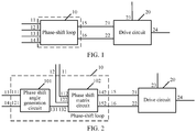
- FIG. 1 is a schematic structural diagram of an inverter anti-islanding control system according to an embodiment of the present invention. As shown in FIG. 1 , the inverter anti-islanding control system described in this embodiment includes a phase-shift loop 10 and a drive circuit 20.
- the phase-shift loop 10 includes a first input end 11, a second input end 12, a third input end 13, a fourth input end 14, a first output end 15, and a second output end 16.
- the drive circuit 20 includes a first input end 21, a second input end 22, a third input end 23, and an output end 24.
- the first output end 15 of the phase-shift loop 10 is connected to the first input end 21 of the drive circuit 20, and the second output end 16 of the phase-shift loop 10 is connected to the second input end 22 of the drive circuit 20.
- the phase-shift loop 10 performs phase shift conversion on an active voltage instruction U d ⁇ and a reactive voltage instruction U q ⁇ based on an inverter alternating current end voltage and frequency protection information in a grid connection standard, to obtain a phase-shifted active voltage instruction U ds ⁇ and a phase-shifted reactive voltage instruction U qs ⁇ .
- U d ⁇ , U q ⁇ , the inverter alternating current end voltage, and the frequency protection information in the grid connection standard reach the phase-shift loop 10 respectively through the first input end 11, the second input end 12, the third input end 13, and the fourth input end 14 of the phase-shift loop 10, U ds ⁇ reaches the first input end 21 of the drive circuit 20 through the first output end 15 of the phase-shift loop 10, and U qs ⁇ reaches the second input end 22 of the drive circuit 20 through the second output end 16 of the phase-shift loop 10.
- the drive circuit 20 generates a drive signal based on U ds ⁇ , U qs ⁇ .
- the drive signal reaches the inverter through the output end 23 of the drive circuit 20, to drive the inverter to output an alternating current voltage having a second frequency, and the second frequency is used to control a connection between the inverter and an electrical network to be disconnected or maintained.
- the frequency protection information in the grid connection standard includes an underfrequency protection threshold f min , an underfrequency protection time T 1 , an overfrequency protection threshold f max , and an overfrequency protection time T 2 . If the second frequency is lower than f min , underfrequency frequency protection is triggered. The connection between the inverter and the electrical network is disconnected after the underfrequency frequency protection is triggered and run for the time T 1 . If the second frequency is higher than f max , overfrequency frequency protection is triggered. The connection between the inverter and the electrical network is disconnected after the overfrequency frequency protection is triggered and run for the time T 2 . If the second frequency is within a range of f min to f max , the connection between the inverter and the electrical network is maintained.
- a new energy device is a photovoltaic array
- a system including the photovoltaic array, an inverter, a transformer, a load, and an electrical network is formed to supply generated power to the electrical network or the load.
- the photovoltaic array generates direct current electric energy
- the inverter converts the direct current electric energy into an alternating current electric energy
- the alternating current electric energy is transferred to the electrical network after being boosted by using the transformer.
- the inverter is still connected to the electrical network because the inverter cannot detect a power-off state of the electrical network, and supplies power to the load as a separate power supply, to be specific, the inverter is in an island state.
- the frequency of the inverter alternating current end voltage can be deviated to the second frequency by using the phase-shift loop, so that the second frequency triggers the frequency protection to disconnect the inverter from the electrical network, to be specific, the inverter is out of the island state.
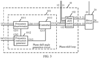
- FIG. 2 is a schematic structural diagram of another inverter anti-islanding control system according to an embodiment of the present invention. As shown in FIG. 2 , the inverter anti-islanding control system described in this embodiment includes a phase-shift loop 10 and a drive circuit 20.
- the phase-shift loop 10 includes a first input end 11, a second input end 12, a third input end 13, a fourth input end 14, a first output end 15, and a second output end 16.
- the drive circuit 20 includes a first input end 21, a second input end 22, a third input end 23, and an output end 24.
- the first output end 15 of the phase-shift loop 10 is connected to the first input end 21 of the drive circuit 20, and the second output end 16 of the phase-shift loop 10 is connected to the second input end 22 of the drive circuit 20.
- the phase-shift loop 10 includes a phase shift angle generation circuit 101 and a phase shift matrix circuit 102.
- the phase shift angle generation circuit 101 includes a first input end 111, a second input end 121, and an output end 131.
- the phase shift matrix circuit 102 includes a first input end 112, a second input end 122, a third input end 132, a first output end 142, and a second output end 152.
- the output end 131 of the phase shift angle generation circuit 101 is connected to the third input end 132 of the phase shift matrix circuit 102.
- the phase shift angle generation circuit 101 generates a phase shift angle based on an inverter alternating current end voltage and frequency protection information in a grid connection standard.
- the inverter alternating current end voltage and the frequency protection information reach the phase shift angle generation circuit 101 respectively through the first input end 111 and the second input end 121 of the phase shift angle generation circuit 101, and the phase shift angle reaches the third input end 132 of the phase shift matrix circuit 102 through the output end 131 of the phase shift angle generation circuit 101.
- the phase shift matrix circuit 102 performs phase shift conversion on an active voltage instruction U d ⁇ and a reactive voltage instruction U q ⁇ based on the phase shift angle, to obtain a phase-shifted active voltage instruction U ds ⁇ and a phase-shifted reactive voltage instruction U qs ⁇ .
- U d ⁇ and U q ⁇ reach the phase shift matrix circuit 102 respectively through the first input end 112 and the second input end 122 of the phase shift matrix circuit 102
- U ds ⁇ reaches the first input end 21 of the drive circuit 20 through the first output end 142 of the phase shift matrix circuit 102
- U qs ⁇ reaches the second input end 22 of the drive circuit 20 through the second output end 152 of the phase shift matrix circuit 102.
- phase shift matrix corresponding to the phase shift matrix circuit 102 is: cos ⁇ sin ⁇ ⁇ sin ⁇ cos ⁇ .
- the frequency of the inverter alternating current end voltage can be deviated to the second frequency by using the phase-shift loop, so that the second frequency triggers frequency protection to disconnect the inverter from an electrical network, to be specific, the inverter is out of the island state.
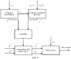
- FIG. 3 is a schematic structural diagram of another inverter anti-islanding control system according to an embodiment of the present invention. As shown in FIG. 3 , the inverter anti-islanding control system described in this embodiment includes a phase-shift loop 10 and a drive circuit 20.
- the phase-shift loop 10 includes a first input end 11, a second input end 12, a third input end 13, a fourth input end 14, a first output end 15, and a second output end 16.
- the drive circuit 20 includes a first input end 21, a second input end 22, a third input end 23, and an output end 24.
- the first output end 15 of the phase-shift loop 10 is connected to the first input end 21 of the drive circuit 20, and the second output end 16 of the phase-shift loop 10 is connected to the second input end 22 of the drive circuit 20.
- the phase-shift loop 10 includes a phase shift angle generation circuit 101 and a phase shift matrix circuit 102.
- the phase shift angle generation circuit 101 includes a first input end 111, a second input end 121, and an output end 131.
- the phase shift matrix circuit 102 includes a first input end 112, a second input end 122, a third input end 132, a first output end 142, and a second output end 152.
- the output end 131 of the phase shift angle generation circuit 101 is connected to the third input end 132 of the phase shift matrix circuit 102.
- the phase shift angle generation circuit 101 includes a frequency discriminator 1011, a frequency instruction generator 1012, and a controller 1013.
- the frequency discriminator 1011 includes an input end 1111 and an output end 1211.
- the frequency instruction generator 1012 includes a first input end 1112, a second output end 1212, and an output end 1312.
- the controller 1013 includes a first input end 1113, a second input end 1213, and an output end 1313.
- the output end 1211 of the frequency discriminator 1011 is connected to the second input end 1212 of the frequency instruction generator 1012 and the first input end 1113 of the controller 1013.
- the output end 1312 of the frequency instruction generator 1012 is connected to the second input end 1213 of the controller 1013.
- the frequency discriminator 1011 outputs a frequency of an inverter alternating current end voltage as a first frequency based on the inverter alternating current end voltage.
- the inverter alternating current end voltage reaches the frequency discriminator 1011 through the input end 1111 of the frequency discriminator 1011, and the first frequency reaches the second input end 1212 of the frequency instruction generator 1012 and the first input end 1113 of the controller 1013 through the output end 1211 of the frequency discriminator 1011.
- the frequency instruction generator 1012 determines a frequency instruction based on the first frequency and frequency protection information in a grid connection standard.
- the frequency protection information reaches the frequency instruction generator 1012 through the first input end 1112 of the frequency instruction generator 1012, and the frequency instruction reaches the second input end 1213 of the controller 1013 through the output end 1312 of the frequency instruction generator 1012.
- the frequency protection information includes an underfrequency protection threshold f min , an underfrequency protection time T 1 , an overfrequency protection threshold f max , and an overfrequency protection time T 2 .
- a normal working frequency range is f min to f max .
- the frequency instruction output by the frequency instruction generator 1012 is the first frequency; or when the first frequency is not within the normal working frequency range and T 1 ⁇ T 2 , the frequency instruction output by the frequency instruction generator 1012 is f min ; or when the first frequency is not within the normal working frequency range and T 1 > T 2 , the frequency instruction output by the frequency instruction generator 1012 is f max .
- the frequency instruction generator sets a frequency protection threshold with a relatively short protection time as the frequency instruction. Consequently, when the inverter outputs an alternating current voltage having a second frequency, the second frequency is deviated to the frequency protection threshold with the relatively short protection time. Therefore, if the second frequency triggers frequency protection, the inverter can be disconnected from the electrical network after the inverter is run for the relatively short time. Therefore, in this embodiment, when an island effect occurs in the inverter, the inverter can be out of an island state as fast as possible.
- the frequency protection information includes an underfrequency protection threshold f min , an underfrequency protection time T 1 , an overfrequency protection threshold f max , and an overfrequency protection time T 2 , and a normal working frequency range is k 1 f min to k 2 f max , where k 1 is greater than 1, k 2 is less than 1, and k 1 f min ⁇ k 2 f max , and the normal working frequency range is enabled to be less than a range of f min to f max .
- k 1 may be 1.1
- k 2 may be 0.9.
- the frequency instruction output by the frequency instruction generator 1012 is the first frequency; or when the first frequency is not within the normal working frequency range and T 1 ⁇ T 2 , the frequency instruction output by the frequency instruction generator 1012 is f min ; or when the first frequency is not within the normal working frequency range and T 1 > T 2 , the frequency instruction output by the frequency instruction generator 1012 is f max .
- FIG. 4 is a schematic flowchart of determining a frequency instruction by a frequency instruction generator.
- a frequency instruction f* is set to f min ; or when T 1 ⁇ T 2 and f > k 1 f min , a frequency instruction f* is set to a first frequency f; or when T 1 > T 2 and f > k 2 f min , a frequency instruction is set to f max ; or when T 1 > T 2 and f ⁇ k 2 f min , a frequency instruction is set to a first frequency f.
- the controller 1013 determines a phase shift angle based on the first frequency and the frequency instruction.
- the phase shift angle reaches the third input end 132 of the phase shift matrix circuit 102 through the output end 1313 of the controller 1013.
- the controller 1013 may be a proportional controller, a proportional integral controller, a proportional derivative controller, or the like.
- the controller 1013 is a proportional integral controller.
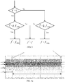
- FIG. 5 is a schematic diagram of a signal flow in the inverter anti-islanding control system described in FIG. 3 .
- the frequency discriminator outputs a frequency of an inverter alternating current end voltage e abc as a first frequency f based on the inverter alternating current end voltage.
- the frequency instruction generator reads frequency protection information in a grid connection standard, and determines a frequency instruction f* based on an underfrequency protection threshold f min , an underfrequency protection time T 1 , an overfrequency protection threshold f max , an overfrequency protection time T 2 , and the first frequency f in the frequency protection information.
- the controller outputs a phase shift angle ⁇ based on the frequency instruction and the first frequency.
- the island phase shift matrix circuit changes, based on the phase shift angle ⁇ , an active voltage instruction U d ⁇ and a reactive voltage instruction U q ⁇ that are output by an active current control unit and a reactive current control unit, and outputs a phase-shifted active voltage instruction U ds ⁇ and a phase-shifted reactive voltage instruction U qs ⁇ .
- the drive circuit generates a drive signal based on U ds ⁇ , U qs ⁇ , and the inverter alternating current end voltage e abc , to drive the inverter to output an alternating current voltage having a second frequency.
- the second frequency is deviated to a frequency protection threshold with a relatively short time relative to the first frequency. If the second frequency triggers underfrequency or overfrequency protection, the inverter is disconnected from the electrical network, to be specific, the inverter is out of an island power generation system, after the inverter is run for an underfrequency/overfrequency protection time.
- FIG. 6a is a schematic waveform diagram of performing island detection without using the inverter anti-islanding control system disclosed in FIG. 3 .
- the first channel of waveform to the third channel of waveform in the figure are waveforms of a three-phase output current of the inverter
- the fourth channel of waveform is a waveform of a current detected at a grid-connected switch.
- the grid-connected switch is turned off, and the current detected at the grid-connected switch is decreased to 0, to be specific, an island effect occurs.
- the inverter is disconnected from the electrical network, and the three-phase output current is decreased to 0, to be specific, the inverter is out of the island state. It can be learned from the waveform diagram that, when the inverter anti-islanding control system described in FIG. 3 is not used, after an island phenomenon occurs in the inverter, the inverter needs to be run for 3.5 seconds and then the inverter can be out of the island state. 3.5 seconds is longer than the island protection time stipulated in the grid connection standard and does not satisfy an island protection requirement in the grid connection standard.
- FIG. 6b is a schematic waveform diagram of performing an island detection experiment by using the inverter anti-islanding control system disclosed in FIG. 3 .
- the first channel of waveform to the third channel of waveform in the figure are waveforms of a three-phase output current of the inverter
- the fourth channel of waveform is a waveform of a current detected at a grid-connected switch.
- the grid-connected switch is turned off, and the current detected at the grid-connected switch is decreased to 0, to be specific, an island effect occurs.
- the inverter is disconnected from the electrical network, and the three-phase output current is decreased to 0, to be specific, the inverter is out of the island state.
- the inverter anti-islanding control system described in FIG. 3 is used, after an island phenomenon occurs in the inverter, the inverter can be out of the island state after being running for only 0.72s. 0.72s is shorter than the island protection time (2s) and satisfies an island protection requirement in the Spanish grid connection standard.
- the frequency instruction generator sets a frequency protection threshold with a relatively short protection time as the frequency instruction. Consequently, when the inverter outputs the alternating current voltage having the second frequency, the second frequency is deviated to the frequency protection threshold with the relatively short protection time. Therefore, if the second frequency triggers frequency protection, the inverter can be disconnected from the electrical network after the inverter is run for the relatively short time. Therefore, in this embodiment, when the island effect occurs in the inverter, the inverter can be out of the island state as fast as possible.
- FIG. 7 is a schematic structural diagram of another inverter anti-islanding control system according to an embodiment of the present invention. As shown in FIG. 7 , the inverter anti-islanding control system described in this embodiment includes a phase-shift loop 10 and a drive circuit 20.
- the phase-shift loop 10 includes a first input end 11, a second input end 12, a third input end 13, a fourth input end 14, a first output end 15, and a second output end 16.
- the drive circuit 20 includes a first input end 21, a second input end 22, a third input end 23, and an output end 24.
- the first output end 15 of the phase-shift loop 10 is connected to the first input end 21 of the drive circuit 20, and the second output end 16 of the phase-shift loop 10 is connected to the second input end 22 of the drive circuit 20.
- the phase-shift loop 10 includes a phase shift angle generation circuit 101 and a phase shift matrix circuit 102.
- the phase shift angle generation circuit 101 includes a first input end 111, a second input end 121, and an output end 131.
- the phase shift matrix circuit 102 includes a first input end 112, a second input end 122, a third input end 132, a first output end 142, and a second output end 152.
- the output end 131 of the phase shift angle generation circuit 101 is connected to the third input end 132 of the phase shift matrix circuit 102.
- the phase shift angle generation circuit 101 includes a frequency discriminator 1011, a frequency instruction generator 1012, and a controller 1013.
- the frequency discriminator 1011 includes an input end 1111 and an output end 1211.
- the frequency instruction generator 1012 includes a first input end 1112, a second output end 1212, and an output end 1312.
- the controller 1013 includes a first input end 1113, a second input end 1213, and an output end 1313.
- the output end 1211 of the frequency discriminator 1011 is connected to the second input end 1212 of the frequency instruction generator 1012 and the first input end 1113 of the controller 1013.
- the output end 1312 of the frequency instruction generator 1012 is connected to the second input end 1213 of the controller 1013.
- the drive circuit 20 includes a phase locked loop 201, a rotation transformation matrix circuit 202, and a drive signal generator 203.
- the phase locked loop 201 includes an input end 211 and an output end 221.
- the rotation transformation matrix circuit 202 includes a first input end 212, a second input end 222, a third input end 232, and an output end 242.
- the drive signal generator 203 includes an input end 213 and an output end 223.
- the output end 221 of the phase locked loop 201 is connected to the third input end 232 of the rotation transformation matrix circuit 202, and the output end 242 of the rotation transformation matrix circuit 202 is connected to the input end 213 of the drive signal generator 203.
- the phase locked loop 201 obtains phase information of the inverter alternating current end voltage based on the inverter alternating current end voltage.
- the inverter alternating current end voltage reaches the phase locked loop 201 through the input end 211 of the phase locked loop 201, and the phase information of the inverter alternating current end voltage reaches the third input end 232 of the rotation transformation matrix circuit 202 through the output end 221 of the phase locked loop 201.
- the rotation transformation matrix circuit 202 converts U ds ⁇ and U qs ⁇ into a three-phase modulation signal based on the phase information of the inverter alternating current end voltage.
- U ds ⁇ and U qs ⁇ reach the rotation transformation matrix circuit 202 through the first input end 212 and the second input end 222 of the rotation transformation matrix circuit 202, and the three-phase modulation signal reaches the input end 213 of the drive signal generator 203 through the output end of the rotation transformation matrix circuit 202.
- the drive signal generator 203 generates the drive signal based on the three-phase modulation signal.
- the drive signal reaches the inverter through the output end 223 of the drive signal generator 203, to drive the inverter to output an alternating current voltage having a second frequency, and the second frequency is used to control a connection between the inverter and an electrical network to be disconnected or maintained.
- the frequency of the inverter alternating current end voltage can be deviated to the second frequency by using the phase-shift loop, so that the second frequency triggers frequency protection to disconnect the inverter from the electrical network, to be specific, the inverter is out of the island state.
- FIG. 8 is a schematic structural diagram of another inverter anti-islanding control system according to an embodiment of the present invention. As shown in FIG. 8 , the inverter anti-islanding control system described in this embodiment includes a phase-shift loop 10 and a drive circuit 20.
- the phase-shift loop 10 includes a first input end 11, a second input end 12, a third input end 13, a fourth input end 14, a first output end 15, and a second output end 16.
- the drive circuit 20 includes a first input end 21, a second input end 22, a third input end 23, and an output end 24.
- the first output end 15 of the phase-shift loop 10 is connected to the first input end 21 of the drive circuit 20, and the second output end 16 of the phase-shift loop 10 is connected to the second input end 22 of the drive circuit 20.
- the phase-shift loop 10 includes a phase shift angle generation circuit 101 and a phase shift matrix circuit 102.
- the phase shift angle generation circuit 101 includes a first input end 111, a second input end 121, and an output end 131.
- the phase shift matrix circuit 102 includes a first input end 112, a second input end 122, a third input end 132, a first output end 142, and a second output end 152.
- the output end 131 of the phase shift angle generation circuit 101 is connected to the third input end 132 of the phase shift matrix circuit 102.
- the phase shift angle generation circuit 101 includes a frequency discriminator 1011, a frequency instruction generator 1012, and a controller 1013.
- the frequency discriminator 1011 includes an input end 1111 and an output end 1211.
- the frequency instruction generator 1012 includes a first input end 1112, a second output end 1212, and an output end 1312.
- the controller 1013 includes a first input end 1113, a second input end 1213, and an output end 1313.
- the output end 1211 of the frequency discriminator 1011 is connected to the second input end 1212 of the frequency instruction generator 1012 and the first input end 1113 of the controller 1013.
- the output end 1312 of the frequency instruction generator 1012 is connected to the second input end 1213 of the controller 1013.
- the drive circuit 20 includes a phase locked loop 201, a rotation transformation matrix circuit 202, and a drive signal generator 203.
- the phase locked loop 201 includes an input end 211 and an output end 221.
- the rotation transformation matrix circuit 202 includes a first input end 212, a second input end 222, a third input end 232, and an output end 242.
- the drive signal generator 203 includes an input end 213 and an output end 223.
- the output end 221 of the phase locked loop 201 is connected to the third input end 232 of the rotation transformation matrix circuit 202, and the output end 242 of the rotation transformation matrix circuit 202 is connected to the input end 213 of the drive signal generator 203.
- the inverter anti-islanding control system further includes: a maximum power point tracking unit 30, a direct current voltage control unit 40, an active current control unit 50, an anti-islanding policy unit 60, and a reactive current control unit 70.
- the maximum power point tracking unit 30 includes a first input end 31, a second input end 32, and an output end 33.
- the direct current voltage control unit 40 includes an input end 41 and an output end 42.
- the active current control unit 50 includes an input end 51 and an output end 52.
- the anti-islanding policy unit 60 includes an output end 61.
- the reactive current control unit 70 includes an input end 71 and an output end 72.
- the output end 33 of the maximum power point tracking unit 30 is connected to the input end 41 of the direct current voltage control unit 40, the output end 42 of the direct current voltage control unit 40 is connected to the input end 51 of the active current control unit 50, and the output end 61 of the anti-islanding policy unit 60 is connected to the input end 71 of the reactive current control unit 70.
- the maximum power point tracking unit 30 determines, based on a direct current voltage and a direct current at an output end of a new energy power generation module, a maximum power point voltage output by the new energy power generation module.
- the direct current voltage and the direct current reach the maximum power point tracking unit 30 through the first input end 31 and the second input end 32 of the maximum power point tracking unit 30, and the maximum power point voltage reaches the input end 41 of the direct current voltage control unit 40 through the output end 33 of the maximum power point tracking unit 30.
- the direct current voltage control unit 40 generates an active current instruction based on the maximum power point voltage.
- the active current instruction reaches the input end 51 of the active current control unit 50 through the output end 42 of the direct current voltage control unit 40.
- the active current control unit 50 generates an active voltage instruction U d ⁇ based on the active current instruction.
- U d ⁇ reaches the first input end 11 of the phase-shift loop 10 through the output end 52 of the active current control unit 50.
- the anti-islanding policy unit 60 is configured to generate a reactive current instruction.
- the reactive current instruction reaches the input end 71 of the reactive current control unit 70 through the output end 61 of the anti-islanding policy unit 60.
- the reactive current control unit 70 is configured to generate a reactive voltage instruction U q ⁇ based on the reactive current instruction.
- U q ⁇ reaches the second input end 12 of the phase-shift loop 10 through the output end 72 of the reactive current control unit 70.
- the frequency of the inverter alternating current end voltage can be deviated to a second frequency by using the phase-shift loop, so that the second frequency triggers frequency protection to disconnect the inverter from an electrical network, to be specific, the inverter is out of the island state.
Landscapes
- Engineering & Computer Science (AREA)
- Power Engineering (AREA)
- Inverter Devices (AREA)
Claims (11)
- Wechselrichter mit einem Inselbildungsschutzsystem für einen Wechselrichter, umfassend:eine Phasenschieberschleife (10) und eine Ansteuerschaltung (20), wobei die Phasenschieberschleife (10) eine erste Eingangsseite (11), eine zweite Eingangsseite (12), eine dritte Eingangsseite (13), eine vierte Eingangsseite (14), eine erste Ausgangsseite (15) und eine zweite Ausgangsseite (16) umfasst; die Ansteuerschaltung (20) eine erste Eingangsseite (21), eine zweite Eingangsseite (22),eine dritte Eingangsseite (23) und eine Ausgangsseite (24) umfasst;die erste Ausgangsseite (15) der Phasenschieberschleife (10) mit der ersten Eingangsseite (21) der Ansteuerschaltung (20) verbunden ist und die zweite Ausgangsseite (16) der Phasenschieberschleife (10) mit der zweiten Eingangsseite (22) der Ansteuerschaltung (20) verbunden ist;die Phasenschieberschleife (10) dazu ausgelegt ist, eine Phasenverschiebungsumwandlung an einem Wirkspannungsbefehl


 die Ansteuerschaltung (20) dazu ausgelegt ist, ein Ansteuersignal basierend auf

- System gemäß Anspruch 1, wobei die Phasenschieberschleife (10) eine Phasenverschiebungswinkel erzeugungsschaltung (101) und eine Phasenverschiebungsmatrixschaltung (102) umfasst, wobei
die Phasenverschiebungswinkelerzeugungsschaltung (101) eine erste Eingangsseite (111), eine zweite Eingangsseite (121) und eine Ausgangsseite (131) umfasst; und die Phasenverschiebungsmatrixschaltung (102) eine erste Eingangsseite (112), eine zweite Eingangsseite (122), eine dritte Eingangsseite (132), eine erste Ausgangsseite (142) und eine zweite Ausgangsseite (152) umfasst;
die Ausgangsseite (131) der Phasenverschiebungswinkelerzeugungsschaltung (101) mit der dritten Eingangsseite (132) der Phasenverschiebungsmatrixschaltung (102) verbunden ist;
die Phasenverschiebungswinkelerzeugungsschaltung (101) dazu ausgelegt ist, einen Phasenverschiebungswinkel basierend auf der Wechselrichter-Wechselstrom-Endspannung und den Frequenzschutzinformationen zu erzeugen, wobei die Wechselrichter-Wechselstrom-Endspannung und die Frequenzschutzinformationen die Phasenverschiebungswinkelerzeugungsschaltung (101) jeweils durch die erste Eingangsseite (111) und die zweite Eingangsseite (121) der Phasenverschiebungswinkel erzeugungsschaltung (101) erreichen und der Phasenverschiebungswinkel die dritte Eingangsseite (131) der Phasenverschiebungsmatrixschaltung (102) durch die Ausgangsseite (131) der Phasenverschiebungswinkelerzeugungsschaltung (101) erreicht; und
die Phasenverschiebungsmatrixschaltung (102) dazu ausgelegt ist, eine Phasenverschiebungsumwandlung an


- System gemäß Anspruch 2, wobei die Phasenverschiebungswinkelerzeugungsschaltung (101) einen Frequenzdiskriminator, einen Frequenzbefehlsgenerator und eine Steuervorrichtung umfasst, wobei der Frequenzdiskriminator eine Eingangsseite und eine Ausgangsseite umfasst; der Frequenzbefehlsgenerator eine erste Eingangsseite, eine zweite Eingangsseite und eine Ausgangsseite umfasst; und die Steuervorrichtung eine erste Eingangsseite, eine zweite Eingangsseite und eine Ausgangsseite umfasst;
die Ausgangsseite des Frequenzdiskriminators mit der zweiten Eingangsseite des Frequenzbefehlsgenerators und der ersten Eingangsseite der Steuervorrichtung verbunden ist und die Ausgangsseite des Frequenzbefehlsgenerators mit der zweiten Eingangsseite der Steuervorrichtung verbunden ist;
der Frequenzdiskriminator dazu ausgelegt ist, eine Frequenz der Wechselrichter-Wechselstrom-Endspannung als eine erste Frequenz basierend auf der Wechselrichter-Wechselstrom-Endspannung auszugeben, wobei die Wechselrichter-Wechselstrom-Endspannung den Frequenzdiskriminator über die Eingangsseite des Frequenzdiskriminators erreicht und die erste Frequenz die zweite Eingangsseite des Frequenzbefehlsgenerators und die erste Eingangsseite der Steuervorrichtung über die Ausgangsseite des Frequenzdiskriminators erreicht;
der Frequenzbefehlsgenerator dazu ausgelegt ist, einen Frequenzbefehl basierend auf der ersten Frequenz und den Frequenzschutzinformationen zu bestimmen, wobei die Frequenzschutzinformationen den Frequenzbefehlsgenerator über die erste Eingangsseite des Frequenzbefehlsgenerators erreichen, und der Frequenzbefehl die zweite Eingangsseite der Steuervorrichtung über die Ausgangsseite des Frequenzbefehlsgenerators erreicht; und
die Steuervorrichtung dazu ausgelegt ist, den Phasenverschiebungswinkel basierend auf der ersten Frequenz und dem Frequenzbefehl zu bestimmen, wobei der Phasenverschiebungswinkel die dritte Eingangsseite der Phasenverschiebungsmatrixschaltung über die Ausgangsseite der Steuervorrichtung erreicht. - System gemäß Anspruch 3, wobei die Frequenzschutzinformationen einen Unterfrequenzschutzschwellenwert fmin, eine Unterfrequenzschutzzeit T1, einen Überfrequenzschutzschwellenwert fmaxund eine Überfrequenzschutzzeit T2 umfassen; ein normaler Arbeitsfrequenzbereich von fmin bis fmax beträgt; und
der Frequenzbefehlsgenerator dazu ausgelegt ist, einen Frequenzbefehl basierend auf der ersten Frequenz zu bestimmen und die Frequenzschutzinformationen umfassen:wenn die erste Frequenz innerhalb des normalen Arbeitsfrequenzbereichs liegt, ist der durch den Frequenzbefehlsgenerator ausgegebene Frequenzbefehl die erste Frequenz; oderwenn die erste Frequenz nicht innerhalb des normalen Arbeitsfrequenzbereichs liegt und T1 < T2 ist, ist der durch den Frequenzbefehlsgenerator ausgegebene Frequenzbefehl fmin; oder wenn die erste Frequenz nicht innerhalb des normalen Arbeitsfrequenzbereichs liegt und T1 > T2 ist, ist der durch den Frequenzbefehlsgenerator ausgegebene Frequenzbefehl fmax. - System gemäß einem der Ansprüche 1 bis 4, wobei die Ansteuerschaltung (20) umfasst:einen Phasenregelkreis (201), eine Drehtransformationsmatrixschaltung (202) und einen Ansteuersignalgenerator (203), wobeider Phasenregelkreis (201) eine Eingangsseite und eine Ausgangsseite umfasst; die Drehtransformationsmatrixschaltung (202) eine erste Eingangsseite, eine zweite Eingangsseite, eine dritte Eingangsseite und eine Ausgangsseite umfasst; und der Ansteuersignalgenerator (203) eine Eingangsseite und eine Ausgangsseite umfasst;die Ausgangsseite des Phasenregelkreises (201) mit der dritten Eingangsseite der Drehtransformationsmatrixschaltung (202) verbunden ist, und die Ausgangsseite der Drehtransformationsmatrixschaltung (202) mit der Eingangsseite des Ansteuersignalgenerators (203) verbunden ist;der Phasenregelkreis (201) dazu ausgelegt ist, Phaseninformationen der Wechselrichter-Wechselstrom-Endspannung basierend auf der Wechselrichter-Wechselstrom-Endspannung zu erhalten, wobei die Wechselrichter-Wechselstrom-Endspannung den Phasenregelkreis (201) über die Eingangsseite des Phasenregelkreises (201) erreicht und die Phaseninformationen der Wechselrichter-Wechselstrom-Endspannung die dritte Eingangsseite der Drehtransformationsmatrixschaltung (202) über die Ausgangsseite des Phasenregelkreises (201) erreichen;die Drehtransformationsmatrixschaltung (202) dazu ausgelegt ist,


 der Ansteuersignalgenerator (203) dazu ausgelegt ist, das Ansteuersignal basierend auf dem dreiphasigen Modulationssignal zu erzeugen, wobei das Ansteuersignal den Wechselrichter über die Ausgangsseite des Ansteuersignalgenerators (203) zum Ansteuern des Wechselrichters erreicht, um die Wechselspannung mit der zweiten Frequenz auszugeben, und die zweite Frequenz dazu verwendet wird, die Verbindung zwischen dem Wechselrichter und dem elektrischen Netzwerk zu steuern, die zu trennen oder aufrechtzuerhalten ist.
 - System gemäß Anspruch 5, wobei das System ferner umfasst:eine Steuereinheit (30) zum Nachführen des maximalen Leistungspunkts, eine Gleichspannungssteuereinheit (40), eine Wirkstromsteuereinheit (50), eine Inselbildungsschutzeinheit (60), und eine Blindstromsteuereinheit (70), wobei die Steuereinheit (30) zum Nachführen des maximalen Leistungspunkts eine erste Eingangsseite, eine zweite Eingangsseite und eine Ausgangsseite umfasst; die Gleichspannungssteuereinheit (40) eine Eingangsseite und eine Ausgangsseite umfasst; die Wirkstromsteuereinheit (50) eine Eingangsseite und eine Ausgangsseite umfasst;die Inselbildungsschutzeinheit (60) eine Ausgangsseite umfasst und die Blindstromsteuereinheit (70) eine Eingangsseite und eine Ausgangsseite umfasst;die Ausgangsseite der Steuereinheit (30) zum Nachführen des maximalen Leistungspunkts mit der Eingangsseite der Gleichspannungssteuereinheit (40) verbunden ist, die Ausgangsseite der Gleichspannungssteuereinheit (40) mit der Eingangsseite der Wirkstromsteuereinheit (50) verbunden ist, und die Ausgangsseite der Inselbildungsschutzeinheit (60) mit der Eingangsseite der Blindstromsteuereinheit (70) verbunden ist;die Steuereinheit (30) zum Nachführen des maximalen Leistungspunkts dazu ausgelegt ist, basierend auf einer Gleichspannung und einem Gleichstrom an einer Ausgangsseite eines Neue-Energie-Stromerzeugungsmoduls eine maximale Leistungspunktspannung zu bestimmen, die durch das Neue-Energie-Stromerzeugungsmodul ausgegeben wird, wobei die Gleichspannung und der Gleichstrom die Steuereinheit (30) zum Nachführen des maximalen Leistungspunkts über die erste Eingangsseite und die zweite Eingangsseite der Steuereinheit (30) zum Nachführen des maximalen Leistungspunkts erreichen und die maximale Leistungspunktspannung die Eingangsseite der Gleichspannungssteuereinheit (40) über die Ausgangsseite der Steuereinheit (30) zum Nachführen des maximalen Leistungspunkts erreicht;die Gleichspannungssteuereinheit (40) dazu ausgelegt ist, einen Wirkstrombefehl basierend auf der maximalen Leistungspunktspannung zu erzeugen, wobei der Wirkstrombefehl die Eingangsseite der Wirkstromsteuereinheit (50) über die Ausgangsseite der Gleichspannungssteuereinheit (40) erreicht;die Wirkstromsteuereinheit (50) dazu ausgelegt ist, den Wirkspannungsbefehl

 die Inselbildungsschutzeinheit (60) dazu ausgelegt ist, einen Blindstrombefehl zu erzeugen, wobei der Blindstrombefehl die Eingangsseite der Blindstromsteuereinheit (70) über die Ausgangsseite der Inselbildungsschutzeinheit (60) erreicht; unddie Blindstromsteuereinheit (70) dazu ausgelegt ist, den Blindspannungsbefehl

- System gemäß einem der Ansprüche 2 bis 6, wobei eine Phasenverschiebungsmatrix entsprechend der Phasenverschiebungsmatrixschaltung:

Δθ der Phasenverschiebungswinkel ist. - System gemäß einem der Ansprüche 2 bis 7, wobei


Δθ der Phasenverschiebungswinkel ist. - System gemäß einem der Ansprüche 1 bis 8, wobei der Wechselrichter einer von einem einphasigen Wechselrichter, einem dreiphasigen Wechselrichter, einem Wechselrichter mit Zwei-Ebenen-Topologie oder einem Wechselrichter mit Multi-Ebenen-Topologie ist.
- System gemäß einem der Ansprüche 3 bis 9, wobei die Steuervorrichtung eine Proportionalsteuervorrichtung, eine Proportional-Integralsteuervorrichtung oder eine Proportional-Differenzialsteuervorrichtung ist.
- Verwendung eines Inselbildungsschutzsystems für einen Wechselrichter in einem Wechselrichter, wobei das Inselbildungsschutzsystem umfasst:eine Phasenschieberschleife (10) und eine Ansteuerschaltung (20), wobei die Phasenschieberschleife (10) eine erste Eingangsseite (11), eine zweite Eingangsseite (12), eine dritte Eingangsseite (13), eine vierte Eingangsseite (14), eine erste Ausgangsseite (15) und eine zweite Ausgangsseite (16) umfasst; die Ansteuerschaltung (20) eine erste Eingangsseite (21), eine zweite Eingangsseite (22), eine dritte Eingangsseite (23) und eine Ausgangsseite (24) umfasst;die erste Ausgangsseite (15) der Phasenschieberschleife (10) mit der ersten Eingangsseite (21) der Ansteuerschaltung (20) verbunden ist und die zweite Ausgangsseite (16) der Phasenschieberschleife (10) mit der zweiten Eingangsseite (22) der Ansteuerschaltung (20) verbunden ist;die Phasenschieberschleife (10) dazu ausgelegt ist, eine Phasenverschiebungsumwandlung an einem Wirkspannungsbefehl


 die Ansteuerschaltung (20) dazu ausgelegt ist, ein Ansteuersignal basierend auf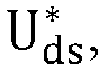

Applications Claiming Priority (2)
| Application Number | Priority Date | Filing Date | Title |
|---|---|---|---|
| CN201611050777.4A CN108110785B (zh) | 2016-11-24 | 2016-11-24 | 一种逆变器反孤岛控制系统 |
| PCT/CN2017/092474 WO2018095046A1 (zh) | 2016-11-24 | 2017-07-11 | 逆变器反孤岛控制系统 |
Publications (3)
| Publication Number | Publication Date |
|---|---|
| EP3537557A1 EP3537557A1 (de) | 2019-09-11 |
| EP3537557A4 EP3537557A4 (de) | 2019-12-04 |
| EP3537557B1 true EP3537557B1 (de) | 2021-04-28 |
Family
ID=62196097
Family Applications (1)
| Application Number | Title | Priority Date | Filing Date |
|---|---|---|---|
| EP17874121.1A Active EP3537557B1 (de) | 2016-11-24 | 2017-07-11 | Inselbildungsschutzsystem für wechselrichter |
Country Status (4)
| Country | Link |
|---|---|
| US (1) | US10637249B2 (de) |
| EP (1) | EP3537557B1 (de) |
| CN (1) | CN108110785B (de) |
| WO (1) | WO2018095046A1 (de) |
Families Citing this family (3)
| Publication number | Priority date | Publication date | Assignee | Title |
|---|---|---|---|---|
| FR3052307B1 (fr) * | 2016-06-07 | 2019-07-12 | Thales | Demarreur generateur sans balais |
| WO2022051892A1 (zh) * | 2020-09-08 | 2022-03-17 | 华为数字能源技术有限公司 | 一种三电平逆变器、控制方法及系统 |
| CN117890723B (zh) * | 2023-12-19 | 2024-08-02 | 安徽拓界电源科技有限公司 | 孤岛检测方法及系统 |
Family Cites Families (36)
| Publication number | Priority date | Publication date | Assignee | Title |
|---|---|---|---|---|
| US6815932B2 (en) * | 2000-10-12 | 2004-11-09 | Capstone Turbine Corporation | Detection of islanded behavior and anti-islanding protection of a generator in grid-connected mode |
| KR20070025269A (ko) * | 2005-09-01 | 2007-03-08 | 울산대학교 산학협력단 | 자동 위상 이동법에 의한 고립운전 검출장치 |
| EP1764894A1 (de) * | 2005-09-19 | 2007-03-21 | ABB Schweiz AG | Verfahren zur Erkennung des Inselbetriebs eines dezentralen Energieerzeugers |
| EP2168230A2 (de) * | 2007-07-16 | 2010-03-31 | Enphase Energy, Inc. | Verfahren und vorrichtung zur inselbildungsverhinderung verteilter stromerzeugnissysteme |
| CN101257209B (zh) | 2008-01-10 | 2010-06-16 | 清华大学深圳研究生院 | 光伏并网发电系统的孤岛运行检测方法 |
| DE102010009709A1 (de) * | 2009-09-09 | 2011-03-24 | Siemens Aktiengesellschaft | Synchronisiereinrichtung und Sychronisierverfahren für den Betrieb von Inselnetzen |
| CN101651337B (zh) | 2009-09-17 | 2011-06-08 | 山东大学 | 基于相位偏移和频率变化的复合型孤岛检测方法 |
| CN101931219B (zh) | 2010-08-24 | 2013-02-06 | 西安交通大学 | 一种基于相位偏移的自抗扰孤岛检测方法 |
| CN101944723A (zh) * | 2010-08-26 | 2011-01-12 | 哈尔滨九洲电气股份有限公司 | 一种光伏并网发电系统的孤岛运行检测方法 |
| US20120091817A1 (en) * | 2010-10-18 | 2012-04-19 | Advanced Energy Industries, Inc. | System, method, and apparatus for ac grid connection of series-connected inverters |
| CN101950985B (zh) * | 2010-11-01 | 2013-07-03 | 上海兆能电力电子技术有限公司 | 单相并网光伏逆变器输出谐波及直流分量的抑制方法 |
| CN102255329B (zh) | 2011-04-14 | 2013-11-20 | 东南大学 | 一种光伏并网系统的孤岛检测方法 |
| KR101243896B1 (ko) * | 2011-09-05 | 2013-03-20 | 카코뉴에너지 주식회사 | 신재생 에너지 발전 시스템 및 그의 단독 운전 방지 방법 |
| US20130077367A1 (en) * | 2011-09-23 | 2013-03-28 | Huibin Zhu | Systems and methods for use in grid fault event control |
| CN102522770B (zh) | 2011-12-04 | 2014-05-28 | 东华大学 | 一种无变压器型的光伏并网检测系统及检测方法 |
| JP5764750B2 (ja) * | 2012-11-16 | 2015-08-19 | パナソニックIpマネジメント株式会社 | リレー動作設定装置、パワーコンディショナ及び分散型電源システム |
| CN103296643B (zh) | 2013-03-19 | 2017-02-22 | 昆明理工大学 | 一种基于广域信息电压相位差比较式孤岛检测及孤岛保护方法 |
| CN103207335B (zh) | 2013-03-21 | 2015-06-03 | 中国农业大学 | 一种基于相位-频率正反馈的孤岛检测方法 |
| CN104215841B (zh) | 2013-05-31 | 2017-02-15 | 阳光电源股份有限公司 | 孤岛检测方法、装置、变流器和分布式发电系统 |
| US20150015072A1 (en) * | 2013-07-12 | 2015-01-15 | Infineon Technologies Austria Ag | Power Converter Circuit and Method |
| US20150094871A1 (en) * | 2013-09-27 | 2015-04-02 | International Business Machines Corporation | Managing devices in micro-grids |
| CN103515981B (zh) | 2013-09-29 | 2016-03-16 | 沈阳工业大学 | 并网光伏发电系统及其自动式相位移孤岛现象检测方法 |
| CN103760434A (zh) | 2013-12-27 | 2014-04-30 | 浙江工业大学 | 一种基于模糊控制的自适应相位偏移孤岛检测方法 |
| CN104753081B (zh) * | 2013-12-30 | 2018-02-06 | 华为技术有限公司 | 一种控制微电网供电的方法和装置 |
| CN103983898A (zh) | 2014-05-19 | 2014-08-13 | 国网宁夏电力公司 | 基于相位突变和主动频率偏移相结合的孤岛检测方法 |
| CN103954870B (zh) | 2014-05-19 | 2016-08-17 | 华北电力大学 | 一种串联谐振与相位跳变相结合的孤岛检测方法 |
| CN104155537B (zh) | 2014-07-04 | 2017-01-18 | 西安工程大学 | 低频正弦相位扰动的孤岛检测方法 |
| CN104198886A (zh) * | 2014-08-15 | 2014-12-10 | 萨瑞新能源技术(苏州)有限公司 | 一种光伏并网发电系统检测孤岛效应的方法及其装置 |
| CN104267315B (zh) * | 2014-10-16 | 2015-11-25 | 山东大学 | 基于主动频率偏移和电压幅值变化的复合型孤岛检测方法 |
| CN104638671B (zh) | 2015-01-16 | 2016-08-17 | 合肥工业大学 | 基于引入粒子群算法及相位扰动的孤岛检测方法 |
| US10333390B2 (en) * | 2015-05-08 | 2019-06-25 | The Board Of Trustees Of The University Of Alabama | Systems and methods for providing vector control of a grid connected converter with a resonant circuit grid filter |
| KR101554630B1 (ko) * | 2015-05-14 | 2015-09-21 | 카코뉴에너지 주식회사 | 병렬 분산 전원용 단독 운전 검출 장치 |
| CN104865479B (zh) * | 2015-06-15 | 2018-06-01 | 江苏方天电力技术有限公司 | 一种孤岛检测方法 |
| CN105182189B (zh) * | 2015-10-29 | 2017-12-12 | 国家电网公司 | 基于电压频率和测量阻抗结合的逆变器扰动式孤岛检测法 |
| CN105467237A (zh) | 2015-11-25 | 2016-04-06 | 东方日立(成都)电控设备有限公司 | 一种基于有功电流扰动的正反馈孤岛检测方法 |
| CN105759175B (zh) * | 2016-04-05 | 2018-11-23 | 中山大学 | 一种带相角偏移正反馈的主动移频式孤岛检测方法 |
-
2016
- 2016-11-24 CN CN201611050777.4A patent/CN108110785B/zh active Active
-
2017
- 2017-07-11 WO PCT/CN2017/092474 patent/WO2018095046A1/zh not_active Ceased
- 2017-07-11 EP EP17874121.1A patent/EP3537557B1/de active Active
-
2019
- 2019-05-23 US US16/420,496 patent/US10637249B2/en active Active
Non-Patent Citations (1)
| Title |
|---|
| None * |
Also Published As
| Publication number | Publication date |
|---|---|
| US20190280484A1 (en) | 2019-09-12 |
| US10637249B2 (en) | 2020-04-28 |
| CN108110785B (zh) | 2021-04-20 |
| EP3537557A4 (de) | 2019-12-04 |
| WO2018095046A1 (zh) | 2018-05-31 |
| CN108110785A (zh) | 2018-06-01 |
| EP3537557A1 (de) | 2019-09-11 |
Similar Documents
| Publication | Publication Date | Title |
|---|---|---|
| US8570003B2 (en) | Double fed induction generator converter and method for suppressing transient in deactivation of crowbar circuit for grid fault ridethrough | |
| US9331487B2 (en) | Method and apparatus for islanding detection for grid tie converters | |
| US11239664B2 (en) | Power conversion system | |
| US9490626B2 (en) | Methods for anti-islanding in distributed-source electrical power generation and distribution systems and electrical systems and apparatus using same | |
| EP3026775B1 (de) | Steuerungsvorrichtung für einen sonnenenergieerzeugungs-wechselrichter | |
| US20140078625A1 (en) | Islanding detection method and system | |
| EP2680425B1 (de) | Leistungsumrichter | |
| EP2680424B1 (de) | Stromrichter | |
| EP3537557B1 (de) | Inselbildungsschutzsystem für wechselrichter | |
| WO2017072593A1 (en) | System and method for improved performance and synchronization of a grid tie inverter | |
| Das et al. | Self-synchronizing control enabling disruption-free operation and seamless mode transitions in wind–solar based hybrid AC/DC microgrid | |
| EP3836331A1 (de) | Stromumwandlungsvorrichtung | |
| JP2023517420A (ja) | グリッド単独運転を検出する方法及び装置 | |
| EP2680426B1 (de) | Sonnenenergieerzeugungssystem | |
| KR102726845B1 (ko) | 수력 발전 계통 연계 시스템 | |
| US11711028B2 (en) | Inverter control device and method | |
| JP6258806B2 (ja) | 系統連系用電力変換装置 | |
| EP3086457B1 (de) | Umrichtersteuerungsvorrichtung | |
| JP2008118809A (ja) | 系統連系用電力変換システムの単独運転保護方法および単独運転保護装置 | |
| WO2021124577A1 (ja) | 電力変換装置 | |
| Mazhari et al. | Locking frequency band exposure method for islanding detection and prevention in distributed generation | |
| EP3160030A1 (de) | Leistungswandlersteuerungsvorrichtung | |
| Das et al. | APSA based self synchronizing control of a reconfigurable hybrid AC/DC microgrid | |
| EP4318905B1 (de) | Gleichstromanschlusskasten, fotovoltaisches stromerzeugungssystem und fehlererkennungsverfahren | |
| CN116754899B (zh) | 一种微电网并网系统电网故障检测方法及其装置 |
Legal Events
| Date | Code | Title | Description |
|---|---|---|---|
| STAA | Information on the status of an ep patent application or granted ep patent |
Free format text: STATUS: THE INTERNATIONAL PUBLICATION HAS BEEN MADE |
|
| PUAI | Public reference made under article 153(3) epc to a published international application that has entered the european phase |
Free format text: ORIGINAL CODE: 0009012 |
|
| STAA | Information on the status of an ep patent application or granted ep patent |
Free format text: STATUS: REQUEST FOR EXAMINATION WAS MADE |
|
| 17P | Request for examination filed |
Effective date: 20190607 |
|
| AK | Designated contracting states |
Kind code of ref document: A1 Designated state(s): AL AT BE BG CH CY CZ DE DK EE ES FI FR GB GR HR HU IE IS IT LI LT LU LV MC MK MT NL NO PL PT RO RS SE SI SK SM TR |
|
| AX | Request for extension of the european patent |
Extension state: BA ME |
|
| A4 | Supplementary search report drawn up and despatched |
Effective date: 20191031 |
|
| RIC1 | Information provided on ipc code assigned before grant |
Ipc: H02J 3/48 20060101ALI20191025BHEP Ipc: H02J 3/50 20060101ALI20191025BHEP Ipc: H02M 1/08 20060101ALI20191025BHEP Ipc: H02J 3/38 20060101AFI20191025BHEP Ipc: H02M 7/5387 20070101ALI20191025BHEP |
|
| DAV | Request for validation of the european patent (deleted) | ||
| DAX | Request for extension of the european patent (deleted) | ||
| GRAP | Despatch of communication of intention to grant a patent |
Free format text: ORIGINAL CODE: EPIDOSNIGR1 |
|
| STAA | Information on the status of an ep patent application or granted ep patent |
Free format text: STATUS: GRANT OF PATENT IS INTENDED |
|
| RIC1 | Information provided on ipc code assigned before grant |
Ipc: H02J 3/38 20060101AFI20201111BHEP Ipc: H02M 7/5387 20070101ALI20201111BHEP Ipc: H02M 1/08 20060101ALI20201111BHEP Ipc: H02J 3/50 20060101ALI20201111BHEP Ipc: H02M 7/48 20070101ALI20201111BHEP Ipc: H02J 3/46 20060101ALI20201111BHEP Ipc: H02J 3/48 20060101ALI20201111BHEP |
|
| INTG | Intention to grant announced |
Effective date: 20201203 |
|
| GRAS | Grant fee paid |
Free format text: ORIGINAL CODE: EPIDOSNIGR3 |
|
| GRAA | (expected) grant |
Free format text: ORIGINAL CODE: 0009210 |
|
| STAA | Information on the status of an ep patent application or granted ep patent |
Free format text: STATUS: THE PATENT HAS BEEN GRANTED |
|
| AK | Designated contracting states |
Kind code of ref document: B1 Designated state(s): AL AT BE BG CH CY CZ DE DK EE ES FI FR GB GR HR HU IE IS IT LI LT LU LV MC MK MT NL NO PL PT RO RS SE SI SK SM TR |
|
| REG | Reference to a national code |
Ref country code: GB Ref legal event code: FG4D |
|
| REG | Reference to a national code |
Ref country code: CH Ref legal event code: EP |
|
| REG | Reference to a national code |
Ref country code: AT Ref legal event code: REF Ref document number: 1388219 Country of ref document: AT Kind code of ref document: T Effective date: 20210515 |
|
| REG | Reference to a national code |
Ref country code: DE Ref legal event code: R096 Ref document number: 602017037834 Country of ref document: DE |
|
| REG | Reference to a national code |
Ref country code: IE Ref legal event code: FG4D |
|
| REG | Reference to a national code |
Ref country code: LT Ref legal event code: MG9D |
|
| REG | Reference to a national code |
Ref country code: AT Ref legal event code: MK05 Ref document number: 1388219 Country of ref document: AT Kind code of ref document: T Effective date: 20210428 |
|
| PG25 | Lapsed in a contracting state [announced via postgrant information from national office to epo] |
Ref country code: FI Free format text: LAPSE BECAUSE OF FAILURE TO SUBMIT A TRANSLATION OF THE DESCRIPTION OR TO PAY THE FEE WITHIN THE PRESCRIBED TIME-LIMIT Effective date: 20210428 Ref country code: LT Free format text: LAPSE BECAUSE OF FAILURE TO SUBMIT A TRANSLATION OF THE DESCRIPTION OR TO PAY THE FEE WITHIN THE PRESCRIBED TIME-LIMIT Effective date: 20210428 Ref country code: NL Free format text: LAPSE BECAUSE OF FAILURE TO SUBMIT A TRANSLATION OF THE DESCRIPTION OR TO PAY THE FEE WITHIN THE PRESCRIBED TIME-LIMIT Effective date: 20210428 Ref country code: BG Free format text: LAPSE BECAUSE OF FAILURE TO SUBMIT A TRANSLATION OF THE DESCRIPTION OR TO PAY THE FEE WITHIN THE PRESCRIBED TIME-LIMIT Effective date: 20210728 Ref country code: AT Free format text: LAPSE BECAUSE OF FAILURE TO SUBMIT A TRANSLATION OF THE DESCRIPTION OR TO PAY THE FEE WITHIN THE PRESCRIBED TIME-LIMIT Effective date: 20210428 Ref country code: HR Free format text: LAPSE BECAUSE OF FAILURE TO SUBMIT A TRANSLATION OF THE DESCRIPTION OR TO PAY THE FEE WITHIN THE PRESCRIBED TIME-LIMIT Effective date: 20210428 |
|
| PG25 | Lapsed in a contracting state [announced via postgrant information from national office to epo] |
Ref country code: PL Free format text: LAPSE BECAUSE OF FAILURE TO SUBMIT A TRANSLATION OF THE DESCRIPTION OR TO PAY THE FEE WITHIN THE PRESCRIBED TIME-LIMIT Effective date: 20210428 Ref country code: PT Free format text: LAPSE BECAUSE OF FAILURE TO SUBMIT A TRANSLATION OF THE DESCRIPTION OR TO PAY THE FEE WITHIN THE PRESCRIBED TIME-LIMIT Effective date: 20210830 Ref country code: LV Free format text: LAPSE BECAUSE OF FAILURE TO SUBMIT A TRANSLATION OF THE DESCRIPTION OR TO PAY THE FEE WITHIN THE PRESCRIBED TIME-LIMIT Effective date: 20210428 Ref country code: NO Free format text: LAPSE BECAUSE OF FAILURE TO SUBMIT A TRANSLATION OF THE DESCRIPTION OR TO PAY THE FEE WITHIN THE PRESCRIBED TIME-LIMIT Effective date: 20210728 Ref country code: SE Free format text: LAPSE BECAUSE OF FAILURE TO SUBMIT A TRANSLATION OF THE DESCRIPTION OR TO PAY THE FEE WITHIN THE PRESCRIBED TIME-LIMIT Effective date: 20210428 Ref country code: RS Free format text: LAPSE BECAUSE OF FAILURE TO SUBMIT A TRANSLATION OF THE DESCRIPTION OR TO PAY THE FEE WITHIN THE PRESCRIBED TIME-LIMIT Effective date: 20210428 Ref country code: IS Free format text: LAPSE BECAUSE OF FAILURE TO SUBMIT A TRANSLATION OF THE DESCRIPTION OR TO PAY THE FEE WITHIN THE PRESCRIBED TIME-LIMIT Effective date: 20210828 Ref country code: GR Free format text: LAPSE BECAUSE OF FAILURE TO SUBMIT A TRANSLATION OF THE DESCRIPTION OR TO PAY THE FEE WITHIN THE PRESCRIBED TIME-LIMIT Effective date: 20210729 |
|
| REG | Reference to a national code |
Ref country code: NL Ref legal event code: MP Effective date: 20210428 |
|
| PG25 | Lapsed in a contracting state [announced via postgrant information from national office to epo] |
Ref country code: RO Free format text: LAPSE BECAUSE OF FAILURE TO SUBMIT A TRANSLATION OF THE DESCRIPTION OR TO PAY THE FEE WITHIN THE PRESCRIBED TIME-LIMIT Effective date: 20210428 Ref country code: CZ Free format text: LAPSE BECAUSE OF FAILURE TO SUBMIT A TRANSLATION OF THE DESCRIPTION OR TO PAY THE FEE WITHIN THE PRESCRIBED TIME-LIMIT Effective date: 20210428 Ref country code: DK Free format text: LAPSE BECAUSE OF FAILURE TO SUBMIT A TRANSLATION OF THE DESCRIPTION OR TO PAY THE FEE WITHIN THE PRESCRIBED TIME-LIMIT Effective date: 20210428 Ref country code: EE Free format text: LAPSE BECAUSE OF FAILURE TO SUBMIT A TRANSLATION OF THE DESCRIPTION OR TO PAY THE FEE WITHIN THE PRESCRIBED TIME-LIMIT Effective date: 20210428 Ref country code: ES Free format text: LAPSE BECAUSE OF FAILURE TO SUBMIT A TRANSLATION OF THE DESCRIPTION OR TO PAY THE FEE WITHIN THE PRESCRIBED TIME-LIMIT Effective date: 20210428 Ref country code: SK Free format text: LAPSE BECAUSE OF FAILURE TO SUBMIT A TRANSLATION OF THE DESCRIPTION OR TO PAY THE FEE WITHIN THE PRESCRIBED TIME-LIMIT Effective date: 20210428 Ref country code: SM Free format text: LAPSE BECAUSE OF FAILURE TO SUBMIT A TRANSLATION OF THE DESCRIPTION OR TO PAY THE FEE WITHIN THE PRESCRIBED TIME-LIMIT Effective date: 20210428 |
|
| REG | Reference to a national code |
Ref country code: DE Ref legal event code: R097 Ref document number: 602017037834 Country of ref document: DE |
|
| REG | Reference to a national code |
Ref country code: CH Ref legal event code: PL |
|
| PLBE | No opposition filed within time limit |
Free format text: ORIGINAL CODE: 0009261 |
|
| STAA | Information on the status of an ep patent application or granted ep patent |
Free format text: STATUS: NO OPPOSITION FILED WITHIN TIME LIMIT |
|
| GBPC | Gb: european patent ceased through non-payment of renewal fee |
Effective date: 20210728 |
|
| PG25 | Lapsed in a contracting state [announced via postgrant information from national office to epo] |
Ref country code: MC Free format text: LAPSE BECAUSE OF FAILURE TO SUBMIT A TRANSLATION OF THE DESCRIPTION OR TO PAY THE FEE WITHIN THE PRESCRIBED TIME-LIMIT Effective date: 20210428 |
|
| REG | Reference to a national code |
Ref country code: BE Ref legal event code: MM Effective date: 20210731 |
|
| 26N | No opposition filed |
Effective date: 20220131 |
|
| PG25 | Lapsed in a contracting state [announced via postgrant information from national office to epo] |
Ref country code: LI Free format text: LAPSE BECAUSE OF NON-PAYMENT OF DUE FEES Effective date: 20210731 Ref country code: GB Free format text: LAPSE BECAUSE OF NON-PAYMENT OF DUE FEES Effective date: 20210728 Ref country code: CH Free format text: LAPSE BECAUSE OF NON-PAYMENT OF DUE FEES Effective date: 20210731 |
|
| PG25 | Lapsed in a contracting state [announced via postgrant information from national office to epo] |
Ref country code: IS Free format text: LAPSE BECAUSE OF FAILURE TO SUBMIT A TRANSLATION OF THE DESCRIPTION OR TO PAY THE FEE WITHIN THE PRESCRIBED TIME-LIMIT Effective date: 20210828 Ref country code: LU Free format text: LAPSE BECAUSE OF NON-PAYMENT OF DUE FEES Effective date: 20210711 Ref country code: FR Free format text: LAPSE BECAUSE OF NON-PAYMENT OF DUE FEES Effective date: 20210731 Ref country code: AL Free format text: LAPSE BECAUSE OF FAILURE TO SUBMIT A TRANSLATION OF THE DESCRIPTION OR TO PAY THE FEE WITHIN THE PRESCRIBED TIME-LIMIT Effective date: 20210428 |
|
| PG25 | Lapsed in a contracting state [announced via postgrant information from national office to epo] |
Ref country code: IT Free format text: LAPSE BECAUSE OF FAILURE TO SUBMIT A TRANSLATION OF THE DESCRIPTION OR TO PAY THE FEE WITHIN THE PRESCRIBED TIME-LIMIT Effective date: 20210428 Ref country code: IE Free format text: LAPSE BECAUSE OF NON-PAYMENT OF DUE FEES Effective date: 20210711 Ref country code: BE Free format text: LAPSE BECAUSE OF NON-PAYMENT OF DUE FEES Effective date: 20210731 |
|
| PG25 | Lapsed in a contracting state [announced via postgrant information from national office to epo] |
Ref country code: CY Free format text: LAPSE BECAUSE OF FAILURE TO SUBMIT A TRANSLATION OF THE DESCRIPTION OR TO PAY THE FEE WITHIN THE PRESCRIBED TIME-LIMIT Effective date: 20210428 |
|
| PG25 | Lapsed in a contracting state [announced via postgrant information from national office to epo] |
Ref country code: HU Free format text: LAPSE BECAUSE OF FAILURE TO SUBMIT A TRANSLATION OF THE DESCRIPTION OR TO PAY THE FEE WITHIN THE PRESCRIBED TIME-LIMIT; INVALID AB INITIO Effective date: 20170711 |
|
| PG25 | Lapsed in a contracting state [announced via postgrant information from national office to epo] |
Ref country code: MK Free format text: LAPSE BECAUSE OF FAILURE TO SUBMIT A TRANSLATION OF THE DESCRIPTION OR TO PAY THE FEE WITHIN THE PRESCRIBED TIME-LIMIT Effective date: 20210428 |
|
| PG25 | Lapsed in a contracting state [announced via postgrant information from national office to epo] |
Ref country code: MT Free format text: LAPSE BECAUSE OF FAILURE TO SUBMIT A TRANSLATION OF THE DESCRIPTION OR TO PAY THE FEE WITHIN THE PRESCRIBED TIME-LIMIT Effective date: 20210428 |
|
| PGFP | Annual fee paid to national office [announced via postgrant information from national office to epo] |
Ref country code: DE Payment date: 20250604 Year of fee payment: 9 |
|
| PG25 | Lapsed in a contracting state [announced via postgrant information from national office to epo] |
Ref country code: TR Free format text: LAPSE BECAUSE OF FAILURE TO SUBMIT A TRANSLATION OF THE DESCRIPTION OR TO PAY THE FEE WITHIN THE PRESCRIBED TIME-LIMIT Effective date: 20210428 |