EP3537177A1 - Dispositif et procédé de commande sans transformateur d'un transducteur ultrasonore - Google Patents
Dispositif et procédé de commande sans transformateur d'un transducteur ultrasonore Download PDFInfo
- Publication number
- EP3537177A1 EP3537177A1 EP18191720.4A EP18191720A EP3537177A1 EP 3537177 A1 EP3537177 A1 EP 3537177A1 EP 18191720 A EP18191720 A EP 18191720A EP 3537177 A1 EP3537177 A1 EP 3537177A1
- Authority
- EP
- European Patent Office
- Prior art keywords
- transducer
- drv
- series
- capacitance
- circuit
- Prior art date
- Legal status (The legal status is an assumption and is not a legal conclusion. Google has not performed a legal analysis and makes no representation as to the accuracy of the status listed.)
- Pending
Links
Images


Classifications
-
- G—PHYSICS
- G01—MEASURING; TESTING
- G01S—RADIO DIRECTION-FINDING; RADIO NAVIGATION; DETERMINING DISTANCE OR VELOCITY BY USE OF RADIO WAVES; LOCATING OR PRESENCE-DETECTING BY USE OF THE REFLECTION OR RERADIATION OF RADIO WAVES; ANALOGOUS ARRANGEMENTS USING OTHER WAVES
- G01S7/00—Details of systems according to groups G01S13/00, G01S15/00, G01S17/00
- G01S7/52—Details of systems according to groups G01S13/00, G01S15/00, G01S17/00 of systems according to group G01S15/00
- G01S7/523—Details of pulse systems
- G01S7/524—Transmitters
-
- B—PERFORMING OPERATIONS; TRANSPORTING
- B06—GENERATING OR TRANSMITTING MECHANICAL VIBRATIONS IN GENERAL
- B06B—METHODS OR APPARATUS FOR GENERATING OR TRANSMITTING MECHANICAL VIBRATIONS OF INFRASONIC, SONIC, OR ULTRASONIC FREQUENCY, e.g. FOR PERFORMING MECHANICAL WORK IN GENERAL
- B06B1/00—Methods or apparatus for generating mechanical vibrations of infrasonic, sonic, or ultrasonic frequency
- B06B1/02—Methods or apparatus for generating mechanical vibrations of infrasonic, sonic, or ultrasonic frequency making use of electrical energy
- B06B1/0207—Driving circuits
- B06B1/0215—Driving circuits for generating pulses, e.g. bursts of oscillations, envelopes
-
- G—PHYSICS
- G01—MEASURING; TESTING
- G01S—RADIO DIRECTION-FINDING; RADIO NAVIGATION; DETERMINING DISTANCE OR VELOCITY BY USE OF RADIO WAVES; LOCATING OR PRESENCE-DETECTING BY USE OF THE REFLECTION OR RERADIATION OF RADIO WAVES; ANALOGOUS ARRANGEMENTS USING OTHER WAVES
- G01S15/00—Systems using the reflection or reradiation of acoustic waves, e.g. sonar systems
- G01S15/88—Sonar systems specially adapted for specific applications
- G01S15/93—Sonar systems specially adapted for specific applications for anti-collision purposes
- G01S15/931—Sonar systems specially adapted for specific applications for anti-collision purposes of land vehicles
-
- B—PERFORMING OPERATIONS; TRANSPORTING
- B06—GENERATING OR TRANSMITTING MECHANICAL VIBRATIONS IN GENERAL
- B06B—METHODS OR APPARATUS FOR GENERATING OR TRANSMITTING MECHANICAL VIBRATIONS OF INFRASONIC, SONIC, OR ULTRASONIC FREQUENCY, e.g. FOR PERFORMING MECHANICAL WORK IN GENERAL
- B06B2201/00—Indexing scheme associated with B06B1/0207 for details covered by B06B1/0207 but not provided for in any of its subgroups
- B06B2201/50—Application to a particular transducer type
- B06B2201/55—Piezoelectric transducer
Definitions
- the invention relates to a transformer-free operating circuit for an ultrasonic transducer (TR).
- TR ultrasonic transducer
- Fig. 1 shows schematically and simplified the driver stage for a prior art ultrasonic transducer. Since the invention only with the drive of the piezoelectric Concerning vibrating element of a transducer, the following also applies to ultrasonic transmitter with a piezoelectric vibrating element.
- the operating voltage (V bat ) is stabilized via a back-up capacitor (C bat ), which is typically chosen to be relatively large.
- the transducer (TR) is driven.
- the fifth transistor (T 5 ) is switched through for this purpose.
- the positive terminal (TR +) of the transducer (TR) is then connected in this first phase via the driver output resistor (R DRV ) to the operating voltage (V bat ).
- the first transistor (T 1 ) and the fourth transistor (T 4 ) are turned on.
- the drive capacitance (C) with its first terminal (C p ) with the operating voltage (V bat ) and with its second terminal (C m ) to the reference potential (GND) is connected.
- the third transistor (T 3 ) and the second transistor (T 2 ) are blocked in this first phase.
- a second phase of the drive phase of the fifth transistor (T 5 ) the first transistor (T 1 ) and the fourth transistor (T 4 ) are disabled. Instead, in this second phase, the second transistor (T 2 ) and the third transistor (T 3 ) are turned on.
- the previously charged to the operating voltage (V bat ) driver capacitance (C) is connected to its first terminal (C p ) to the reference potential (GND) and connected to your second terminal (C m ) to the driver output (DRV).
- the driver output performs a voltage jump by twice the magnitude of the voltage of the operating voltage (V bat ) below the reference potential (GND).
- the first and second phases of the drive phases now preferably alternate with the resonant frequency of the transducer circuit, consisting of the driver output resistance (R DRV ), the transducer capacitance (C TR ) and the transducer (TR).
- the piezoelectric vibrating element of the transducer (TR) is set in vibration.
- the reception phase follows. In this case, at least the fifth transistor (T 5 ) and the third transistor (T 3 ) are blocked. As a result, no more electrical energy is transferred to the transducer (TR).
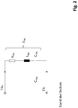
- Fig. 2 shows an equivalent circuit diagram known from the prior art for an ultrasonic transducer (TR).
- the equivalent circuit has a shunt capacitance (C TRp ), a series resistance (R TRs ), a series capacitance (C TRs ), and a series inductance (L TRs ).
- the ultrasonic transducer is connected via a positive terminal (TR +) and a negative terminal (TR-).
- TR + positive terminal
- TR- negative terminal
- the invention has for its object to provide a solution that does not have the above disadvantage of the prior art and has other advantages.
- the value of the driver output impedance is appropriately selected by appropriate selection of the driver output inductance of the driver output impedance, which may possibly also have a driver output capacitance, so that the two aforementioned oscillator circuits are critically coupled.
- the above object is achieved by the use of the aforementioned device, wherein it is provided that the transducer (TR) after the end of a drive phase with an AC voltage between the positive terminal (TR +) of the transducer (TR) and the negative terminal (TR- ) of the transducer (TR) which has a peak-to-peak value which is more than twice the magnitude of the operating voltage (V bat ) of the device at the beginning of the decay phase of the transducer (TR).
- V DRV output inductance
- the third-order oscillatory system formed by the drive output resistance (R DRV ), the transducer capacitance (C TR ) and the transducer is unfavorable for operation, and although it is more complex but less expensive is to use a vibrating system of fourth order.
- the transducer in the circuit after Fig. 1 can, as already described, by an equivalent circuit of a series circuit of a series capacitance (C TRs ), a series inductance (L TRs ) and a series resistor (R TRs ) are shown with a parallel to this series connection parallel capacitance (C TRp ).
- the series resistance (R TRs ) represents the mechanical losses and the acoustic radiation of the transducer (TR).
- the voltage across this series resistor (R s ) should be maximized to maximize the range of an ultrasonic parking aid.
- the parallel capacitance (C TRp ) is typically dominated by the transducer- external transducer capacitance (C TR ).
- the transducer (TR) has a series and a parallel resonance.
- the series resonance is determined by the series resonant circuit of series capacitance (C TRs ) and series inductance (L TRs ) and to a lesser extent by the series resistance (R TRs ) and thus the sound radiation.
- a further pole point is now generated by a further energy store in the transmission system.
- an additional output inductance L DRV
- R DRV driver output resistance
- This output inductance (L DRV ) forms a second series resonant circuit with the transducer capacitance (C TR ).
- the output inductance (L DRV ) is connected to the series resonant circuit of the transducer (TR) by means of the positive transducer terminal (TR +) (for simplicity, assume that the transducer capacitance (C TR ) and shunt capacitance (C TRp ) of the transducer Transducers (TR) through the transducer capacity (C TR ) are well represented). Possibly. So here is the term transducer capacitance (C TR ) to be replaced by the parallel circuit of transducer capacitance (C TR ) and parallel capacitance (C TRp ) of the transducer (TR). However, it is further assumed that the transducer capacitance (C TR ) is substantially greater than the shunt capacitance (C TRp ) of the transducer (TR).
- the output inductance (LDRV), the transducer capacitance (C TR ), the series capacitance of the transducer (TR), and the series inductance of the transducer (TR) thus form a fourth order oscillatory system.
- the standardized coupling factor is ⁇ 1
- the normalized coupling factor is 1.
- the normalized coupling factor is equal to the quotient of coupling factor and damping.
- the coupling factor describes how much two oscillating circuits are inductively coupled.
- the output inductance (L DRV ) must therefore have a defined inductance and quality that causes this case of critical coupling.
- the output inductance (L DRV ) is thus characterized in that it forms a series resonant circuit together with the transducer capacitance (C TR ). Since it is a fourth-order system, it is recommended that the poles be determined by an appropriate numerical approximation in dependence.
- the area of critical coupling is an operating point that can never be exactly met due to manufacturing tolerances of the various components. Therefore, the resonant frequency of the series resonance of the transducer (TR) should never exceed 3dB in addition to the maximum of the frequency dependent impedance of output inductance (L DRV ), transducer capacitance (C TR ) plus shunt capacitance (C TRp ) of the transducer (TR), series capacitance of the transducer (TR) and series inductance of the transducer (TR) are.
- the transducers (TR) have a frequency bandwidth of typically +/- 1 kHz. These transducer frequencies should therefore preferably deviate by no more than 3dB from the optimum in the expected oscillation amplitude.
- On the Driver output resistance (R DRV ) is preferably set the bandwidth and the output inductance (L DRV ), the frequency of the oscillation.
- an operating circuit for an ultrasound transducer which includes a drive or driver circuit, for example, consisting of the backup capacitor (C bat ), the transistors (T 1 , T 2 , T 3 , T 4 , T 5 ), and a transducer capacitance (C TR ) connected in parallel with the transducer ( TR ).
- the drive circuit further has a first terminal (GND) and a second terminal (DRV).
- the drive circuit has a driver output resistance (R DRV ).
- This driver output resistance (R DRV ) is in the FIGS. 1 and 3 discreetly drawn. However, the parasitic resistances of the transistors can contribute to the value of this driver output resistance (R DRV ).
- the driver output resistance (R DRV ) can therefore also be realized in whole or in part by the output resistance of the drive circuit at its second output (DRV).
- the internal resistances of the transistors that is to say the output resistance of the drive circuit, can also be supplemented by an additional driver output resistance, which is connected in series with the second output (DRV) of the drive circuit, to the actual driver output resistance (R DRV ).
- the FIGS. 1 and 3 are thus to be understood as simplified symbolic representations in order to illustrate the principle of the invention.
- the transducer capacitance (C TR ) may be formed by the capacitance present in the transducer (TR) and need not be present as a discrete element in the circuit.
- the FIGS. 1 and 3 are thus to be understood as simplified symbolic representations in order to illustrate the principle of the invention.
- a positive terminal (TR +) of the transducer (TR) is connected to the second terminal (DRV) of the drive circuit such that the driver output resistance (R DRV ) is effectively connected between the positive terminal (TR +) of the transducer (TR) and the second terminal (TR).
- DRV) of the drive circuit can be considered switched.
- a negative terminal (TR-) of the transducer (TR) is connected to the first terminal (GND) of the drive circuit.
- a (drive) output inductance (L DRV ) is effectively considered to be connected between the positive terminal (TR +) of the transducer (TR) and the second terminal (DRV) of the drive circuit in series with the driver output resistance (R DRV ) can. Furthermore, it is provided according to the invention that the value of the output inductance (L DRV ) is dimensioned such that the two series resonant circuits are critically coupled.
- critical coupling has been discussed above with a frequency deviation of less than +/- 3dB in terms of impedance change. If a circuit is in this area, it is critically coupled in the sense of the invention.
- the operating circuit may be arranged to operate the transducer between its positive terminal (TR +) and its negative terminal (TR-) with an AC amplitude having a peak-to-peak value after the end of a drive phase which, at the beginning of the decay phase in the temporal connection to the drive phase of the transducer (TR) amounts to more than twice the amount of the voltage of the operating voltage (V bat ) against a reference potential (GND).
- TR + positive terminal
- TR- negative terminal
- the preferred operating circuit for a transducer thus has a capacitive energy store (C TR ) and an inductive energy store (L DRV ) in order to be able to generate this level.
- the core of the invention is the control of an ultrasonic transmitter (possibly also coupled with receiving function, as is the case with an ultrasonic transducer) by means of at least two critically coupled LC resonant circuits.
- the one LC resonant circuit is characterized by the parasitic components (L TRs ) and (C TRs ) of the ultrasonic transmitter implemented.
- the equivalent circuit of the ultrasonic transmitter has a series connection of an inductance, a capacitance and a resistor, parallel to which there is a further capacitance (C TRp ).
- a driver output inductance (L DRV ) is introduced, so that there are two coupled LC resonant circuits.
- the essential finding of the invention is to be seen in the driver output impedance Z DRV , which has a resistive component R DRV , an inductive component L DRV and optionally a capacitive component C DRV (see the circuit in FIG Fig. 3 ), to tune to the transducer impedance Z TR .
- the transducer impedance Z TR is composed of the impedance Z TRs of the series resonant circuit of the equivalent circuit of the transducer with R TRs , C TRs and L TRs of the transducer, the parallel capacitance C TRp of the equivalent circuit of the transducer and an external, with the terminals Tr + and Tr - The transducer further connected parallel capacitance C TR .
- the tuning or adaptation of both resonant circuits is such that the two resonant circuits are critically coupled.
- the driver output inductance L DRV is selected accordingly, since typically the transducer impedance is given by the hardware of the transducer. Due to the critical coupling, the active power introduced into the transducer series resistor R TRs and thus output by it is optimized.
- FIGS. 4 and 5 is a variant of the circuit after Fig. 3 in which, in order to maximize the active power in the transducer series resistor R TRs, the bridge driver circuit (driver stage TS) has the same internal resistance both in the positive half-wave of the drive and in its negative half-wave to maximize the energy transfer to the transducer, since then an optimum Resistance matching can be achieved by suitable choice of the network.
- the measuring circuit part of the circuit according to Fig. 3 is in the FIGS. 4 and 5 Not shown.
- the transducer TR together with the impedance Z TR form a bandpass filter BPF.
- the four outer curves show a minimum in the middle of a larger bandwidth, which represents the case of supercritical coupling.
- the upper middle curve shows the result of the critical coupling, which is characterized by a plateau (approximately) over an average bandwidth.
- Fig. 8 shows the decay of the transducer TR in the same circuit as that of Fig. 7 with the difference that now according to the difference between Fig. 1 and Fig. 3 an output inductance L DRV has been inserted into the lead of the transducer TR and that its value has been determined to be the coupling between the series resonant circuit of series capacitance C TRs and series inductance L TRs of the transducer TR on the one hand and the series resonant peak of output inductance LDRV and transducer capacitance C TR and parallel capacitance C TRp of the transducer TR on the other hand is critical.
- a peak-to-peak value V SS of 31.4V ( Fig. 3 ) which is significantly above the 12V of the construction of the Fig. 7 ( Fig. 1 ) lies.
- the corresponding voltage levels of the peak values are again shown as dashed lines.
- Fig. 9 shows the conditions particularly well.
- Fig. 9a the voltage across the transducer TR between positive transducer terminal TR + and negative transducer terminal TR- (shown in dashed lines) is shown against the reference potential GND for the case without additional output inductance L DRV .
- Fig. 9a the voltage at the transducer TR between positive transducer terminal TR + and negative transducer terminal TR- (shown in solid line) against the reference potential GND for the case MIT additional output inductance L DRV is shown.
- Fig. 9b is the acoustic impulse that propagates within the electric transducer model ( Fig. 2 ) as voltage across the series resistor R TRs .
- These are simulation curves. Dashed again the level without output inductance L DRV is shown, pulled through the level with output inductance L DRV . At optimum conditions, a ratio of 1: 4 results in the acoustic output voltage without administratinduktsammlung L DRV to the level with output inductance L DRV .
Landscapes
- Engineering & Computer Science (AREA)
- Radar, Positioning & Navigation (AREA)
- Remote Sensing (AREA)
- Physics & Mathematics (AREA)
- Mechanical Engineering (AREA)
- Computer Networks & Wireless Communication (AREA)
- General Physics & Mathematics (AREA)
- Acoustics & Sound (AREA)
- Apparatuses For Generation Of Mechanical Vibrations (AREA)
Applications Claiming Priority (2)
| Application Number | Priority Date | Filing Date | Title |
|---|---|---|---|
| DE102018105283.9A DE102018105283A1 (de) | 2018-03-07 | 2018-03-07 | Vorrichtung und Verfahren zur übertragerfreien Ansteuerung eines Ultraschalltransducers mit Signalen mit einer Amplitude oberhalb der doppelten Versorgungsspannungsamplitude |
| DE102018105284.7A DE102018105284A1 (de) | 2018-03-07 | 2018-03-07 | Vorrichtung und Verfahren zur übertragerfreien Ansteuerung eines Ultraschalltransducers mit Signalen mit einer Amplitude oberhalb der doppelten Versorgungsspannungsamplitude |
Publications (1)
| Publication Number | Publication Date |
|---|---|
| EP3537177A1 true EP3537177A1 (fr) | 2019-09-11 |
Family
ID=63449378
Family Applications (1)
| Application Number | Title | Priority Date | Filing Date |
|---|---|---|---|
| EP18191720.4A Pending EP3537177A1 (fr) | 2018-03-07 | 2018-08-30 | Dispositif et procédé de commande sans transformateur d'un transducteur ultrasonore |
Country Status (2)
| Country | Link |
|---|---|
| EP (1) | EP3537177A1 (fr) |
| CN (1) | CN110238016B (fr) |
Cited By (2)
| Publication number | Priority date | Publication date | Assignee | Title |
|---|---|---|---|---|
| US11389831B2 (en) | 2020-08-05 | 2022-07-19 | Elmos Semiconductor Se | Transformerless ultrasonic transducer activation with only one external energy store |
| EP4258017A1 (fr) | 2022-04-08 | 2023-10-11 | Elmos Semiconductor SE | Dispositif de commande d'un transducteur ultrasonore et dispositif de mesure ultrasonore muni d'un tel dispositif de commande pour le transducteur ultrasonore |
Citations (3)
| Publication number | Priority date | Publication date | Assignee | Title |
|---|---|---|---|---|
| US20100242611A1 (en) * | 2009-03-31 | 2010-09-30 | Denso Corporation | Ultrasonic sensor |
| EP2312572A1 (fr) * | 2009-10-08 | 2011-04-20 | Valeo Schalter und Sensoren GmbH | Convertisseur ultrasonique |
| EP2743725A1 (fr) * | 2012-12-14 | 2014-06-18 | ELMOS Semiconductor AG | Dispositif à ultrasons |
Family Cites Families (1)
| Publication number | Priority date | Publication date | Assignee | Title |
|---|---|---|---|---|
| JP4983171B2 (ja) * | 2005-11-15 | 2012-07-25 | セイコーエプソン株式会社 | 静電型トランスデューサ、容量性負荷の駆動回路、回路定数の設定方法、超音波スピーカ、および指向性音響システム |
-
2018
- 2018-08-30 EP EP18191720.4A patent/EP3537177A1/fr active Pending
-
2019
- 2019-03-06 CN CN201910167267.2A patent/CN110238016B/zh active Active
Patent Citations (3)
| Publication number | Priority date | Publication date | Assignee | Title |
|---|---|---|---|---|
| US20100242611A1 (en) * | 2009-03-31 | 2010-09-30 | Denso Corporation | Ultrasonic sensor |
| EP2312572A1 (fr) * | 2009-10-08 | 2011-04-20 | Valeo Schalter und Sensoren GmbH | Convertisseur ultrasonique |
| EP2743725A1 (fr) * | 2012-12-14 | 2014-06-18 | ELMOS Semiconductor AG | Dispositif à ultrasons |
Cited By (2)
| Publication number | Priority date | Publication date | Assignee | Title |
|---|---|---|---|---|
| US11389831B2 (en) | 2020-08-05 | 2022-07-19 | Elmos Semiconductor Se | Transformerless ultrasonic transducer activation with only one external energy store |
| EP4258017A1 (fr) | 2022-04-08 | 2023-10-11 | Elmos Semiconductor SE | Dispositif de commande d'un transducteur ultrasonore et dispositif de mesure ultrasonore muni d'un tel dispositif de commande pour le transducteur ultrasonore |
Also Published As
| Publication number | Publication date |
|---|---|
| CN110238016B (zh) | 2021-11-16 |
| CN110238016A (zh) | 2019-09-17 |
Similar Documents
| Publication | Publication Date | Title |
|---|---|---|
| DE60012566T2 (de) | Schaltnetzteilumwandler mit einem piezoelektrischen umwandler | |
| DE69104799T2 (de) | Piezoelektrische Anregeschaltung mit Benutzung von resonanter Energieübertragung. | |
| DE102016218021A1 (de) | Vorrichtung und Verfahren zum Bestimmen einer Resonanzfrequenz einer LC-Schaltung in situ durch Vergleichen von Spannungs- und Strompolartitätsänderungen | |
| EP2984503B1 (fr) | Procédé de mesure par ultrason, notamment comme aide au stationnement pour véhicules, et systèmes de mesure par ultrason | |
| EP2743725B1 (fr) | Dispositif à ultrasons | |
| DE1286627B (de) | Rueckgekoppelter Hochfrequenzgenerator mit einem piezoelektrischen Schwinger | |
| WO2003077414A2 (fr) | Amplificateur de puissance | |
| EP2780125B1 (fr) | Transducteur ultrasonique et dispositif correspondant de surveillance de l'environnement d'un véhicule | |
| DE2813729C2 (de) | Verfahren und Schaltungsanordnung zur Anregung von Ultraschallschwingern, die in der Impuls-Echo-Technik eingesetzt werden | |
| EP3537177A1 (fr) | Dispositif et procédé de commande sans transformateur d'un transducteur ultrasonore | |
| DE2823155C2 (de) | Treiberschaltung für einen piezoelektrischen Schwinger | |
| EP2881181A1 (fr) | Procédé de détermination de paramètres électriques d'un syntoniseur pour convertisseur à ultrasons | |
| EP2872263B1 (fr) | Étage de sortie pour l'adaptation d'un signal electrique alternatif d'un generateur ultrasonore | |
| EP0133570B1 (fr) | Circuit d'attaque pour transducteur piézoélectrique | |
| EP2390634B1 (fr) | Dispositif de fonctionnement d'une unité pivotante d'un résonateur à vibrations | |
| DE2604497A1 (de) | Oszillator mit phasenumkehrschwingungswandler | |
| DE102018105283A1 (de) | Vorrichtung und Verfahren zur übertragerfreien Ansteuerung eines Ultraschalltransducers mit Signalen mit einer Amplitude oberhalb der doppelten Versorgungsspannungsamplitude | |
| DE102018105284A1 (de) | Vorrichtung und Verfahren zur übertragerfreien Ansteuerung eines Ultraschalltransducers mit Signalen mit einer Amplitude oberhalb der doppelten Versorgungsspannungsamplitude | |
| DE102017214697A1 (de) | Schaltungsanordnung und Ansteuerungsverfahren für einen piezohydraulischen Aktor | |
| EP2692451B1 (fr) | Circuit électrique pour le fonctionnement d'une unité émettrice-réceptrice | |
| DE102010062930A1 (de) | Verfahren zur Erfassung eines Objekts in einem Umfeld und Vorrichtung zur Erzeugung eines Ultraschallsignals | |
| EP4004567B1 (fr) | Procédé et générateur pour la caractérisation d'un système oscillant | |
| DE102004060577B4 (de) | Schaltung und Verfahren zum Erzeugen eines Strompulses in einem Wellenleiter | |
| AT165266B (de) | Impulserzeuger zum Erzeugen von Impulsen vorbestimmter Dauer in Vorbestimmten Zeitabständen | |
| EP1498702B1 (fr) | Dispositif de terrain pour mesurer et/ou surveiller une grandeur de procéssus |
Legal Events
| Date | Code | Title | Description |
|---|---|---|---|
| PUAI | Public reference made under article 153(3) epc to a published international application that has entered the european phase |
Free format text: ORIGINAL CODE: 0009012 |
|
| STAA | Information on the status of an ep patent application or granted ep patent |
Free format text: STATUS: THE APPLICATION HAS BEEN PUBLISHED |
|
| AK | Designated contracting states |
Kind code of ref document: A1 Designated state(s): AL AT BE BG CH CY CZ DE DK EE ES FI FR GB GR HR HU IE IS IT LI LT LU LV MC MK MT NL NO PL PT RO RS SE SI SK SM TR |
|
| AX | Request for extension of the european patent |
Extension state: BA ME |
|
| STAA | Information on the status of an ep patent application or granted ep patent |
Free format text: STATUS: REQUEST FOR EXAMINATION WAS MADE |
|
| 17P | Request for examination filed |
Effective date: 20191220 |
|
| RBV | Designated contracting states (corrected) |
Designated state(s): AL AT BE BG CH CY CZ DE DK EE ES FI FR GB GR HR HU IE IS IT LI LT LU LV MC MK MT NL NO PL PT RO RS SE SI SK SM TR |
|
| RAP1 | Party data changed (applicant data changed or rights of an application transferred) |
Owner name: ELMOS SEMICONDUCTOR SE |
|
| RIN1 | Information on inventor provided before grant (corrected) |
Inventor name: FRIEMANN, UWE Inventor name: KAPOOR, NIRON |
|
| STAA | Information on the status of an ep patent application or granted ep patent |
Free format text: STATUS: EXAMINATION IS IN PROGRESS |
|
| 17Q | First examination report despatched |
Effective date: 20211104 |