EP3537138A1 - Quantum dot biosensor - Google Patents
Quantum dot biosensor Download PDFInfo
- Publication number
- EP3537138A1 EP3537138A1 EP17867342.2A EP17867342A EP3537138A1 EP 3537138 A1 EP3537138 A1 EP 3537138A1 EP 17867342 A EP17867342 A EP 17867342A EP 3537138 A1 EP3537138 A1 EP 3537138A1
- Authority
- EP
- European Patent Office
- Prior art keywords
- quantum dot
- biosensor
- insulating layer
- ligand
- source electrode
- Prior art date
- Legal status (The legal status is an assumption and is not a legal conclusion. Google has not performed a legal analysis and makes no representation as to the accuracy of the status listed.)
- Granted
Links
Images


Classifications
-
- G—PHYSICS
- G01—MEASURING; TESTING
- G01N—INVESTIGATING OR ANALYSING MATERIALS BY DETERMINING THEIR CHEMICAL OR PHYSICAL PROPERTIES
- G01N27/00—Investigating or analysing materials by the use of electric, electrochemical, or magnetic means
- G01N27/26—Investigating or analysing materials by the use of electric, electrochemical, or magnetic means by investigating electrochemical variables; by using electrolysis or electrophoresis
- G01N27/28—Electrolytic cell components
- G01N27/30—Electrodes, e.g. test electrodes; Half-cells
- G01N27/327—Biochemical electrodes, e.g. electrical or mechanical details for in vitro measurements
- G01N27/3275—Sensing specific biomolecules, e.g. nucleic acid strands, based on an electrode surface reaction
- G01N27/3278—Sensing specific biomolecules, e.g. nucleic acid strands, based on an electrode surface reaction involving nanosized elements, e.g. nanogaps or nanoparticles
-
- G—PHYSICS
- G01—MEASURING; TESTING
- G01N—INVESTIGATING OR ANALYSING MATERIALS BY DETERMINING THEIR CHEMICAL OR PHYSICAL PROPERTIES
- G01N27/00—Investigating or analysing materials by the use of electric, electrochemical, or magnetic means
- G01N27/26—Investigating or analysing materials by the use of electric, electrochemical, or magnetic means by investigating electrochemical variables; by using electrolysis or electrophoresis
- G01N27/403—Cells and electrode assemblies
- G01N27/414—Ion-sensitive or chemical field-effect transistors, i.e. ISFETS or CHEMFETS
- G01N27/4145—Ion-sensitive or chemical field-effect transistors, i.e. ISFETS or CHEMFETS specially adapted for biomolecules, e.g. gate electrode with immobilised receptors
-
- G—PHYSICS
- G01—MEASURING; TESTING
- G01N—INVESTIGATING OR ANALYSING MATERIALS BY DETERMINING THEIR CHEMICAL OR PHYSICAL PROPERTIES
- G01N27/00—Investigating or analysing materials by the use of electric, electrochemical, or magnetic means
- G01N27/26—Investigating or analysing materials by the use of electric, electrochemical, or magnetic means by investigating electrochemical variables; by using electrolysis or electrophoresis
- G01N27/403—Cells and electrode assemblies
- G01N27/414—Ion-sensitive or chemical field-effect transistors, i.e. ISFETS or CHEMFETS
- G01N27/4146—Ion-sensitive or chemical field-effect transistors, i.e. ISFETS or CHEMFETS involving nanosized elements, e.g. nanotubes, nanowires
-
- G—PHYSICS
- G01—MEASURING; TESTING
- G01N—INVESTIGATING OR ANALYSING MATERIALS BY DETERMINING THEIR CHEMICAL OR PHYSICAL PROPERTIES
- G01N27/00—Investigating or analysing materials by the use of electric, electrochemical, or magnetic means
- G01N27/26—Investigating or analysing materials by the use of electric, electrochemical, or magnetic means by investigating electrochemical variables; by using electrolysis or electrophoresis
- G01N27/403—Cells and electrode assemblies
- G01N27/414—Ion-sensitive or chemical field-effect transistors, i.e. ISFETS or CHEMFETS
- G01N27/4148—Integrated circuits therefor, e.g. fabricated by CMOS processing
-
- G—PHYSICS
- G01—MEASURING; TESTING
- G01N—INVESTIGATING OR ANALYSING MATERIALS BY DETERMINING THEIR CHEMICAL OR PHYSICAL PROPERTIES
- G01N33/00—Investigating or analysing materials by specific methods not covered by groups G01N1/00 - G01N31/00
- G01N33/48—Biological material, e.g. blood, urine; Haemocytometers
- G01N33/50—Chemical analysis of biological material, e.g. blood, urine; Testing involving biospecific ligand binding methods; Immunological testing
- G01N33/53—Immunoassay; Biospecific binding assay; Materials therefor
- G01N33/543—Immunoassay; Biospecific binding assay; Materials therefor with an insoluble carrier for immobilising immunochemicals
- G01N33/54313—Immunoassay; Biospecific binding assay; Materials therefor with an insoluble carrier for immobilising immunochemicals the carrier being characterised by its particulate form
- G01N33/54346—Nanoparticles
-
- G—PHYSICS
- G01—MEASURING; TESTING
- G01N—INVESTIGATING OR ANALYSING MATERIALS BY DETERMINING THEIR CHEMICAL OR PHYSICAL PROPERTIES
- G01N33/00—Investigating or analysing materials by specific methods not covered by groups G01N1/00 - G01N31/00
- G01N33/48—Biological material, e.g. blood, urine; Haemocytometers
- G01N33/50—Chemical analysis of biological material, e.g. blood, urine; Testing involving biospecific ligand binding methods; Immunological testing
- G01N33/53—Immunoassay; Biospecific binding assay; Materials therefor
- G01N33/543—Immunoassay; Biospecific binding assay; Materials therefor with an insoluble carrier for immobilising immunochemicals
- G01N33/54366—Apparatus specially adapted for solid-phase testing
- G01N33/54373—Apparatus specially adapted for solid-phase testing involving physiochemical end-point determination, e.g. wave-guides, FETS, gratings
-
- G—PHYSICS
- G01—MEASURING; TESTING
- G01N—INVESTIGATING OR ANALYSING MATERIALS BY DETERMINING THEIR CHEMICAL OR PHYSICAL PROPERTIES
- G01N33/00—Investigating or analysing materials by specific methods not covered by groups G01N1/00 - G01N31/00
- G01N33/48—Biological material, e.g. blood, urine; Haemocytometers
- G01N33/50—Chemical analysis of biological material, e.g. blood, urine; Testing involving biospecific ligand binding methods; Immunological testing
- G01N33/53—Immunoassay; Biospecific binding assay; Materials therefor
- G01N33/543—Immunoassay; Biospecific binding assay; Materials therefor with an insoluble carrier for immobilising immunochemicals
- G01N33/54366—Apparatus specially adapted for solid-phase testing
- G01N33/54373—Apparatus specially adapted for solid-phase testing involving physiochemical end-point determination, e.g. wave-guides, FETS, gratings
- G01N33/5438—Electrodes
-
- G—PHYSICS
- G01—MEASURING; TESTING
- G01N—INVESTIGATING OR ANALYSING MATERIALS BY DETERMINING THEIR CHEMICAL OR PHYSICAL PROPERTIES
- G01N33/00—Investigating or analysing materials by specific methods not covered by groups G01N1/00 - G01N31/00
- G01N33/48—Biological material, e.g. blood, urine; Haemocytometers
- G01N33/50—Chemical analysis of biological material, e.g. blood, urine; Testing involving biospecific ligand binding methods; Immunological testing
- G01N33/58—Chemical analysis of biological material, e.g. blood, urine; Testing involving biospecific ligand binding methods; Immunological testing involving labelled substances
- G01N33/588—Chemical analysis of biological material, e.g. blood, urine; Testing involving biospecific ligand binding methods; Immunological testing involving labelled substances with semiconductor nanocrystal label, e.g. quantum dots
-
- H—ELECTRICITY
- H10—SEMICONDUCTOR DEVICES; ELECTRIC SOLID-STATE DEVICES NOT OTHERWISE PROVIDED FOR
- H10D—INORGANIC ELECTRIC SEMICONDUCTOR DEVICES
- H10D30/00—Field-effect transistors [FET]
- H10D30/01—Manufacture or treatment
- H10D30/014—Manufacture or treatment of FETs having zero-dimensional [0D] or one-dimensional [1D] channels, e.g. quantum wire FETs, single-electron transistors [SET] or Coulomb blockade transistors
-
- H—ELECTRICITY
- H10—SEMICONDUCTOR DEVICES; ELECTRIC SOLID-STATE DEVICES NOT OTHERWISE PROVIDED FOR
- H10D—INORGANIC ELECTRIC SEMICONDUCTOR DEVICES
- H10D30/00—Field-effect transistors [FET]
- H10D30/60—Insulated-gate field-effect transistors [IGFET]
-
- H—ELECTRICITY
- H10—SEMICONDUCTOR DEVICES; ELECTRIC SOLID-STATE DEVICES NOT OTHERWISE PROVIDED FOR
- H10D—INORGANIC ELECTRIC SEMICONDUCTOR DEVICES
- H10D30/00—Field-effect transistors [FET]
- H10D30/60—Insulated-gate field-effect transistors [IGFET]
- H10D30/67—Thin-film transistors [TFT]
- H10D30/6757—Thin-film transistors [TFT] characterised by the structure of the channel, e.g. transverse or longitudinal shape or doping profile
-
- H—ELECTRICITY
- H10—SEMICONDUCTOR DEVICES; ELECTRIC SOLID-STATE DEVICES NOT OTHERWISE PROVIDED FOR
- H10D—INORGANIC ELECTRIC SEMICONDUCTOR DEVICES
- H10D62/00—Semiconductor bodies, or regions thereof, of devices having potential barriers
- H10D62/10—Shapes, relative sizes or dispositions of the regions of the semiconductor bodies; Shapes of the semiconductor bodies
- H10D62/117—Shapes of semiconductor bodies
- H10D62/118—Nanostructure semiconductor bodies
Definitions
- the present invention relates to a biosensor, and particularly, relates to a biosensor using quantum dots.
- quantum dots control their size, they can easily control energy bandgaps, thereby being used as a light emitting material by using such characteristics.
- the quantum dots can generate electric charges by absorbing light of various wavelengths, and thus can be utilized as a material for a biosensor and a light detecting sensor in addition to the light emitting material.
- a biosensor comprising a substrate, a gate electrode provided on the substrate, an insulating layer provided on the gate electrode, a source electrode and a drain electrode, provided on the insulating layer, respectively, an n-type channel provided between the source electrode and the drain electrode, and a quantum dot layer provided on the n-type channel and provided so as to have electronic transition energy capable of resonating with vibration energy of a target biological material.
- the quantum dot constituting the quantum dot layer is a colloidal quantum dot.
- the biosensor may further comprise a collecting part for collecting a biological material to be analyzed, which is provided on the quantum dot layer.
- a biosensor comprising a substrate, a gate electrode provided on the substrate, an insulating layer provided on the gate electrode, a source electrode and a drain electrode, provided on the insulating layer, respectively, and a quantum dot layer provided so as to electrically connect the source electrode and the drain electrode and provided so as to have electronic transition energy capable of resonating with vibration energy of a target biological material.
- the quantum dot constituting the quantum dot layer is a colloidal quantum dot.
- the biosensor may further comprise a collecting part for collecting a biological material to be analyzed, which is provided on the quantum dot layer.
- the biosensor related to at least one example of the present invention can measure the current change of the quantum dot layer depending on the electronic-vibarational energy transfer between the quantum dot layer and the target biomolecules, thereby detecting the biological material.
- the electric charges of the collecting part can be effectively transferred to the sensing part, and the efficiency of the biosensor can be improved.
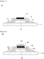
- Figure 1 is a schematic sectional view showing a biosensor (10) according to a first example of the present invention.
- the present invention provides a biosensor (100) comprising a quantum dot layer formed on an n-type channel.
- the quantum dot layer is provided so as to have electronic transition energy capable of resonating with vibration energy of a target biological material.
- the biosensor (10) related to the first example comprises a substrate (11), a gate electrode (14), an insulating layer (18), a source electrode (12), a drain electrode (13), an n- type channel (15), and a quantum dot layer (16).
- the biosensor (10) related to one example of the present invention comprises a substrate (11), a gate electrode (14) provided on the substrate (11), an insulating layer (18) provided on the gate electrode (14), and a source electrode (12) and a drain electrode (13), provided on the insulating layer (18), respectively.
- the biosensor (10) comprises an n-type channel (15) provided between the source electrode (12) and the drain electrode (13), and a quantum dot layer (16) provided so that the current flows and provided on the n-type channel (15).
- the n-type channel (15) is provided to electrically connect the source electrode (12) and the drain electrode (13).
- the quantum dot layer (16) is provided so as to have the electronic transition energy (in-band electronic transition energy) capable of resonating with the vibration energy of the target biological material.
- the quantum dot layer (16) may also be provided to electrically connect the source electrode (12) and the drain electrode (13) and the quantum dot layer (16) may also be provided so as not to electrically connect the source electrode (12) and the drain electrode (13).
- the quantum dot layer (16) is one arranged such that a number of quantum dots having a spherical shape form a layer, where the quantum dots can easily control an energy gap of an electron structure by controlling the size and composition thereof.
- the operation principle of the biosensor (10) using the quantum dots is to detect the current flowing in the quantum dot layer in real time and to use the current change of the quantum dot layer (16).
- the biosensor (10) using the quantum dots it is combined with a field-effect thin film transistor (TFT), which can be utilized.
- TFT field-effect thin film transistor
- the potential difference is generated when the potential of a quantum dot layer (16) is changed according to electronic-vibrational energy transfer between the quantum dot layer (16) and a target biological material.
- the quantum dot layer (16) may be formed in a film form.
- the change of the functional group occurring on the surface of the quantum dot layer (16) changes the potential of the quantum dots, where electrons convert this fine potential change into the current change of a conduction channel of the n-type channel to amplify it.
- the change of the surface potential at the quantum dots indicates the current change in the thin film transistor soon and also appears as a change in threshold voltage, which can be measured and applied as the biosensor.
- a conduction channel is formed in the n-type channel, through which electrons can move between the source electrode (12) and the drain electrode (13).
- the potential of the quantum dots may also affect the n-type conduction channel, thereby affecting the threshold voltage.
- the biosensor (10) can observe the potential difference induced in the quantum dot layer (16) when the current is measured in real time between the source electrode (12) and the gate electrode (14), which is provided so as to measure the current changed according to the specific electronic-vibrational energy transfer transferred from the target biomolecules to the quantum dot layer (16).
- the current to be measured causes the current change, as the in-band transition energy of the quantum dots is absorbed by vibration of the specific functional group of the target biomolecule.
- the increase of the potential by the vibration of the target biomolecule is a new and highly feasible measurement method, where the potential value is proportional to the concentration of the biomolecules.
- the energy transfer is by coupling between the quantum dot layer (16) and the biomolecule vibration
- information on the physical distance between the biomolecule and the quantum dot layer (16) can also be measured.
- the usable n-type channel (15) in the present invention may consist of any one of n-type materials selected from the group consisting of IGZO, ZnO, ZTO, IZO, IHZO, AIN, InN, GaN and InGaN.
- the n-type channel (15) consisted of IGZO is preferred, because it has excellent optical transparency, amorphous structure and high electron mobility, and quantum dots can also be directly functionalized on the IGZO channel.
- the IGZO channel can directly function as an active matrix backplane, which has an advantage that a separate integration process can be omitted.
- colloidal quantum dots are used.
- colloidal quantum dots they can be formed by a simple method such as spin coating on the n-type channel (15), and the quantum dots can be uniformly distributed.
- the biosensor (10) related to one example of the present invention can use the quantum dot layer (16) having electronic transition in the infrared region, especially the mid-infrared region.
- quantum dots capable of absorbing light in the infrared region particularly a wavelength of 1000 nm to 20 ⁇ m, and preferably a wavelength of 1000 nm to 8000 nm, can be used by adjusting the type or size of the quantum dots.
- the colloidal quantum dots can be processed in a large area at low cost, it is preferred to use the colloidal quantum dots in the present invention.
- ligand-substituted quantum dots can be used as the quantum dots.
- the quantum dot may be substituted with at least one ligand of an organic ligand and an inorganic ligand.
- An example of the ligand, which is the quantum dot may include EDT (ethanedithol), BDT (butanethiol), MPA (mercaptocarboxylic acid), CTAB (Cetyltrimethylammonium bromide), HTAC (hexadecyltrimethylammonium chloride), TBAI (tetrabutylammonium iodide) or Na2S.
- the quantum dot has a structure surrounded by an oleic acid ligand for dispersion and stability of the colloidal solution.
- the quantum dots in this state can also be applied to the biosensor, but since the oleic acid ligand has a long chain structure, electrons generated in the quantum dots are disturbed to move to the n-type channel (15). Therefore, it is preferred to substitute the ligand with a ligand having a shorter chain structure.
- a method may be used, in which the ligand is substituted by forming the quantum dot surrounded by the oleic acid ligand on the n-type channel (15) and then reacting it with the ligand.
- the organic material ligand of the colloidal quantum dot layer may be substituted with a monomolecular organic ligand or inorganic ligand to improve accessibility of the target biomolecule and to facilitate resonance of the vibration mode of the functional group in the biomolecule and the in-band transition of the quantum dot layer.
- a bidentate ligand such as EDT, BDT or MPA as described above will be used as the organic ligand for electric charge transfer, which may be mixed with an inorganic ligand to form the film structure of the colloidal quantum dot layer uniformly.
- the used oranic ligands may be substituted with halogen ions such as Br - , Cl - or I - .
- the substitution process can be performed at room temperature by allowing the halogen ions to exist on the film composed of the colloidal quantum dot layer surrounded by the organic ligands for a few minutes.
- the thickness of the film can be increased sequentially, and the thickness can be from 10 nm to 300 nm.
- the halogen is an atomic ligand, it has no vibration motion by the ligand, so that it may remove a molecule to cause resonance phenomenon with the target biomolecule in the mid-infrared region. Accordingly, it is possible to obtain more improved and stable electric signals.
- a method using a polarity difference between a polar solution and a non-polar solution may be used.
- the colloidal quantum dot solution modified with non-polar organic ligands is stirred with the polar inorganic ligand solution at room temperature, the polar ligands are modified on the surface of the colloidal quantum dots and the dielectric constant of the colloidal quantum dots is increased.
- colloidal quantum dots modified with the inorganic ligands are present in the polar solution.
- the colloidal quantum dot solution modified with the polar inorganic ligands has an advantage that the colloidal solution can be coated on the surface.
- the insulating layer (18) may be formed of SiO2, Al2O3, TiO2, ZrO2, HfO2 or SiNx, and the like.
- the gate electrode (14) may be formed of a metal, which may be selected, for example, from the group consisting of Cr, Mo, Al, Ti/Au, Ag, Cu, and Pt.
- the source electrode (12) and the drain electrode (13) may be formed of a metal, respectively, which may be selected, for example, from the group consisting of Cr, Ti/Au, Mo, Al, Ag, Cu, Pt and W.
- the remaining structures other than the insulating layer (18), the n-type channel (15), the quantum dot layer (16), and the source and drain electrodes (12, 13), as described above are not particularly limited as long as they can be usually used in the biosensor (10).
- the substrate (11) a glass substrate or a plastic substrate may be used, which is not particularly limited as long as it is applied to the biosensor (10). Also, the arrangement of each component in the biosensor (10) is not particularly limited as long as it is applied to the conventional biosensor (100).
- Figure 2 is a schematic sectional view showing a biosensor (100) according to a second example of the present invention.
- the biosensor (100) comprises a substrate (110), a gate electrode (140), an insulating layer (180), a source electrode (120), a drain electrode (130), an n-type channel (150), and a quantum dot layer (160) and a collecting part (170). That is, the biosensor (100) according to the second example may further comprise a collecting part (170) for collecting a target biological material, which is provided in the quantum dot layer (160).
- the other components are the same as those of the biosensor (10) described in the first example.
- the biosensor (100) related to the second example comprises a substrate (110), a gate electrode (140) provided on the substrate (110), an insulating layer (180) provided on the gate electrode (140), and a source electrode (120) and a drain electrode (130), provided on the insulating layer (180), respectively.
- the biosensor (100) comprises an n-type channel (150) provided between the source electrode (120) and the drain electrode (130) so as to electrically connect the source electrode (120) and the drain electrode (130).
- the source electrode (120) and the drain electrode (130) are provided over the insulating layer (180) and the n-type channel (150), respectively.
- the biosensor (100) comprises a quantum dot layer (160) provided so that the current flows, provided on the n-type channel (150) and provided so as to have electronic transition energy capable of resonating with vibration energy of a target biological material, and a collecting part (170) for collecting the target biological material, which is provided in the quantum dot layer (160).
- the collecting part (170) may comprise a plurality of collection molecules. Also, the plurality of collection molecules may be immobilized on the curved surface portion of the quantum dot. That is, the quantum dot layer (160) may be provided to have a curved surface. Furthermore, the quantum dot layer (160) may be produced in a film form.
- the current change of the quantum dot layer causes its electrons to move to the conduction channel of the n-type channel to generate a change in the threshold voltage, which can be measured and applied as the biosensor.
- a conduction channel is formed in the n-type channel (150), through which electrons can move between the source electrode (120) and the drain electrode (130).
- the biosensor (100) according to the present invention is provided so as to measure the changed current, by a real-time measurement of the current flowing in the quantum dot layer (160), where a fine potential difference is induced in the quantum dot layer (160) according to a specific electric-vibrational energy transfer between the target biomolecules collected in the collecting part and the quantum dot layer (160) and the current is changed in the n-type channel (150).
- the current to be measured causes the current change, as the in-band transition energy is absorbed by vibration of the specific functional group of the target biomolecule.
- the potential change in the quantum dots by the vibration of the target biomolecule is a new and highly feasible measurement method, where the change of the current values is proportional to the concentration of the biomolecule.
- the advantage of the thin film transistor by the quantum dot layer (160) in this manner is that it can characteristically respond to biomolecule changes of a specific energy and amplify the signal.
- the energy transfer is by coupling between the quantum dot layer (160) and the biomolecule vibration
- information on the physical distance between the biomolecule and the quantum dot layer (160) can also be measured.
- the insulating layer (180) may also be formed of SiO2, Al2O3, TiO2, ZrO2, HfO2 or SiNx, and the like.
- the gate electrode (140) may be formed of a metal, which may be, for example, selected from the group consisting of Cr, Mo, Al, Ti/Au, Ag, Cu and Pt.
- the source electrode (120) and the drain electrode (130) may be each formed of a metal, which may be, for example, selected from the group consisting of Cr, Ti/Au, Mo, Al, Ag, Cu, Pt and W.
- the remaining structures other than the insulating layer (180), the n-type channel (150), the quantum dot layer (160), the collecting part (170), and the source and drain electrodes (120, 130), as described above, are not particularly limited as long as they can be usually used in the biosensor (100).
- the substrate (110) a glass substrate or a plastic substrate may be used, which is not particularly limited as long as it is applied to the biosensor (100). Also, the arrangement of each component in the biosensor (100) is not particularly limited as long as it is applied to the conventional biosensor (100).
- collection molecules may be immobilized on the quantum dot layer (160).
- the collection molecules can specifically bind to the target biological material to be analyzed and collect the biological material.
- the reaction between the collection molecules and the biological material may be, for example, nucleic acid hybridization, an antigen-antibody reaction or an enzyme binding reaction.
- the biological material may be immobilized on the surface of the collection molecule.
- the collection molecules may be, for example, proteins, cells, viruses, nucleic acid organic molecules or inorganic molecules.
- the protein may be, for example, an antigen, an antibody, a substrate protein, an enzyme or a coenzyme.
- the collection molecules are nucleic acids
- the nucleic acid may be, for example, DNA, RNA, PNA, LNA or a hybrid thereof.
- the method for immobilizing the collection molecules (25) on the surface of the quantum dot layer chemical adsorption, covalent-binding, electric binding (electrostatic attraction), copolymerization or an avidin-biotin affinity system, and the like may be utilized.
- a functional group may be provided to immobilize the collection molecules on the surface of the quantum dot layer (160).
- the functional group may be, for example, a carboxyl group (-COOH), a thiol group (-SH), a hydroxyl group (-OH), a silane group (Si-H), an amine group (-NH) or an epoxy group.
- Figure 3 is a schematic sectional view showing a biosensor (200) related to a third example of the present invention.
- the biosensor (200) comprises a substrate (210), a gate electrode (240) provided on the substrate (210), an insulating layer (280) provided on the gate electrode (240), and a source electrode (220) and a drain electrode (230), provided on the insulating layer (280), respectively.
- the biosensor (200) comprises a quantum dot layer (260) positioned on the insulating layer (280), provided so that the current flows between the source electrode (220) and the drain electrode (230), and provided so as to have electronic transition energy capable of resonating with vibration energy of a target biological material.
- the biosensor (200) may further comprise a collecting part (270) for collecting a target biological material, which is provided in the quantum dot layer (260).
- the n-type layer (150) may not be provided and the quantum dot layer (260) electrically connects the source electrode (220) and the drain electrode (230).
- Figures 4 and 5 are graphs showing detection results of cysteine.
- the measurement was performed by depositing an HgSe sample on the thin film transistor (TFT) element by a spin coating method.
- the threshold voltage of the blank state has a value smaller than the threshold voltage after HgSe_HDA is deposited, and thus it can be confirmed that the driving energy is changed.
- the thin film transistor (TFT) element is an element using colloidal quantum dots synthesized by a chemical wet method as an active layer, where the material comprises a semiconductor compound of Group II-VI, a semiconductor compound of Group III-V, a semiconductor compound of Group IV-VI, a semiconductor compound of Group IV or a combination thereof.
- a specific quantum dot is a quantum dot nanoparticle characterized by one or more selected from the group consisting of AuS, AuSe, AuTe, AgS, AgSe, AgTe, AgO, CuS, CuSe, CuTe, CuO, CdS, CdSe, CdTe, ZnS, ZnSe, ZnTe, ZnO, HgS, HgSe, HgTe, AuSeS, AuSeTe, AuSTe, AgSeS, AgSeTe, AgSTe, CuSeS, CuSeTe, CuSTe, CdSeS, CdSeTe, CdSTe, ZnSeS, ZnSeTe, ZnSTe, HgSeS, HgSeTe, HgSTe, AuAgS, AuAgSe, AuAgTe, AuCuS, AuCuSe, AuCuTe, AuZnS, AuZnSe, Au
- the surface of the quantum dot produced by the chemical wet method is surrounded by an organic or inorganic ligand, which can be substituted to change chemical and physical properties.
- the biological material can be selectively detected by using the property changed as the surface of the quantum dot is substituted with various ligands.
- a spin coating method is used as the method of applying quantum dots to a biosensor.
- the quantum dots may be deposited on the surface of the sensor through interlayer deposition and utilized as an active layer to detect biological materials. If a solution, in which a biomolecule to be detected is dissolved, is applied on the sensor spin-coated with the quantum dots, a ligand substitution reaction takes place on the surface of the quantum dot, whereby as the electrical property of the active layer changes, it can be confirmed that the threshold voltage changes.
- the electrical characteristics of the sensor can be measured using the thin film transistor (TFT) element and a semiconductor analyzer.
- the quantum dots may be deposited on the element designed such that as the measured voltage changes the gate voltage between - 10V and 10V, the electrical characteristic change of the active layer may be measured, thereby measuring the changed value to this, and then they may detect the electrical characteristic change by applying a material to be detected to the surface.
- the voltage value of the gate due to the characteristics of the TFT element, it is also possible to detect various different types of biological materials utilizing the characteristics of the deposited state of other materials as well as the HgSe quantum dots used in this experimental example.
- the threshold voltage change is measured by substituting the ligand for the n-type doped material using the characteristics of HgSe.
- the measured current value has an off current of 10 -8 and an on current of 10 -4 , which is a phenomenon that appears as the biological material applied on the surface causes the change in the property of the active layer.
- the p-type active layer is utilized, it is also possible to apply the voltage value in the reverse direction of 10 to -10 V and when the voltage having a higher or lower on/off point is required, the measurement is possible while changing the voltage.
- the biosensor related to at least one example of the present invention can measure the current change of the quantum dot layer depending on the electronic-vibarational energy transfer between the quantum dot layer and the target biomolecules, thereby detecting the biological material.
Landscapes
- Health & Medical Sciences (AREA)
- Life Sciences & Earth Sciences (AREA)
- Chemical & Material Sciences (AREA)
- Engineering & Computer Science (AREA)
- Immunology (AREA)
- Molecular Biology (AREA)
- Physics & Mathematics (AREA)
- Pathology (AREA)
- General Physics & Mathematics (AREA)
- General Health & Medical Sciences (AREA)
- Biochemistry (AREA)
- Analytical Chemistry (AREA)
- Biomedical Technology (AREA)
- Urology & Nephrology (AREA)
- Hematology (AREA)
- Nanotechnology (AREA)
- Chemical Kinetics & Catalysis (AREA)
- Electrochemistry (AREA)
- Microelectronics & Electronic Packaging (AREA)
- Microbiology (AREA)
- Medicinal Chemistry (AREA)
- Food Science & Technology (AREA)
- Cell Biology (AREA)
- Biotechnology (AREA)
- Spectroscopy & Molecular Physics (AREA)
- Crystallography & Structural Chemistry (AREA)
- Materials Engineering (AREA)
- Computer Hardware Design (AREA)
- Thin Film Transistor (AREA)
- Investigating Or Analyzing Materials By The Use Of Electric Means (AREA)
- Measuring Or Testing Involving Enzymes Or Micro-Organisms (AREA)
- Apparatus Associated With Microorganisms And Enzymes (AREA)
Abstract
Description
- The present invention relates to a biosensor, and particularly, relates to a biosensor using quantum dots.
- The present application claims the benefit of priority based on Korean Patent Application No.
10-2016-0144849 filed on November 2, 2016 10-2017-0145154 filed on November 2, 2017 - As quantum dots control their size, they can easily control energy bandgaps, thereby being used as a light emitting material by using such characteristics. In addition, the quantum dots can generate electric charges by absorbing light of various wavelengths, and thus can be utilized as a material for a biosensor and a light detecting sensor in addition to the light emitting material.
- On the other hand, research and development, and investment for monitoring metabolites, such as immunoglobulin E, which are small biomolecules, or specific biological materials such as glucose, modified genes, cancer cells or environmental hormones in real time are being actively conducted.
- There are electrochemical biosensors, piezoelectric biosensors, optical biosensors or thermal biosensors, and the like as technical methods of commonly used biosensors, and in many cases, they may change equilibrium to a real-time sample concentration by destroying the sample during measurement. In addition, because of detection through additional biological markers, additional procedures for adding biological marker materials are required, which have a disadvantage in that the density of the grafted biological marker is low.
- It is a problem to be solved by the present invention to provide a biosensor capable of inducing a fine potential difference to a current change and measuring it, wherein the potential difference is generated when the potential of a quantum dot layer is changed according to electronic-vibrational energy transfer between the quantum dot layer and target biomolecules.
- In addition, it is another problem to be solved by the present invention to provide a biosensor capable of effectively transferring electric charges of a collecting part to a sensing part.
- To solve the above-described problems, according to one aspect of the present invention, there is provided a biosensor comprising a substrate, a gate electrode provided on the substrate, an insulating layer provided on the gate electrode, a source electrode and a drain electrode, provided on the insulating layer, respectively, an n-type channel provided between the source electrode and the drain electrode, and a quantum dot layer provided on the n-type channel and provided so as to have electronic transition energy capable of resonating with vibration energy of a target biological material.
- Also, the quantum dot constituting the quantum dot layer is a colloidal quantum dot.
- Furthermore, the biosensor may further comprise a collecting part for collecting a biological material to be analyzed, which is provided on the quantum dot layer.
- In addition, according to another aspect of the present invention, there is provided a biosensor comprising a substrate, a gate electrode provided on the substrate, an insulating layer provided on the gate electrode, a source electrode and a drain electrode, provided on the insulating layer, respectively, and a quantum dot layer provided so as to electrically connect the source electrode and the drain electrode and provided so as to have electronic transition energy capable of resonating with vibration energy of a target biological material. Also, the quantum dot constituting the quantum dot layer is a colloidal quantum dot. Furthermore, the biosensor may further comprise a collecting part for collecting a biological material to be analyzed, which is provided on the quantum dot layer.
- As described above, according to the biosensor related to at least one example of the present invention, it can measure the current change of the quantum dot layer depending on the electronic-vibarational energy transfer between the quantum dot layer and the target biomolecules, thereby detecting the biological material. In addition, the electric charges of the collecting part can be effectively transferred to the sensing part, and the efficiency of the biosensor can be improved.
-
-
Figure 1 is a schematic sectional view showing a biosensor according to a first example of the present invention. -
Figure 2 is a schematic sectional view showing a biosensor according to a second example of the present invention. -
Figure 3 is a schematic sectional view showing a biosensor according to a third example of the present invention. -
Figures 4 and5 are graphs showing detection results of cysteine. - Hereinafter, a biosensor according to one example of the present invention will be described in detail with reference to the accompanying drawings.
- In addition, the same or similar reference numerals are given to the same or corresponding components regardless of reference numerals, of which redundant explanations will be omitted, and for convenience of explanation, the size and shape of each constituent member as shown may be exaggerated or reduced.
-
Figure 1 is a schematic sectional view showing a biosensor (10) according to a first example of the present invention. - The present invention provides a biosensor (100) comprising a quantum dot layer formed on an n-type channel. In addition, the quantum dot layer is provided so as to have electronic transition energy capable of resonating with vibration energy of a target biological material.
- Referring to
Figure 1 , the biosensor (10) related to the first example comprises a substrate (11), a gate electrode (14), an insulating layer (18), a source electrode (12), a drain electrode (13), an n- type channel (15), and a quantum dot layer (16). - Specifically, the biosensor (10) related to one example of the present invention comprises a substrate (11), a gate electrode (14) provided on the substrate (11), an insulating layer (18) provided on the gate electrode (14), and a source electrode (12) and a drain electrode (13), provided on the insulating layer (18), respectively. Also, the biosensor (10) comprises an n-type channel (15) provided between the source electrode (12) and the drain electrode (13), and a quantum dot layer (16) provided so that the current flows and provided on the n-type channel (15).
- Also, the n-type channel (15) is provided to electrically connect the source electrode (12) and the drain electrode (13).
- Furthermore, the quantum dot layer (16) is provided so as to have the electronic transition energy (in-band electronic transition energy) capable of resonating with the vibration energy of the target biological material.
- In addition, the quantum dot layer (16) may also be provided to electrically connect the source electrode (12) and the drain electrode (13) and the quantum dot layer (16) may also be provided so as not to electrically connect the source electrode (12) and the drain electrode (13).
- The quantum dot layer (16) is one arranged such that a number of quantum dots having a spherical shape form a layer, where the quantum dots can easily control an energy gap of an electron structure by controlling the size and composition thereof.
- The operation principle of the biosensor (10) using the quantum dots is to detect the current flowing in the quantum dot layer in real time and to use the current change of the quantum dot layer (16). For example, in the case of the biosensor (10) using the quantum dots, it is combined with a field-effect thin film transistor (TFT), which can be utilized.
- Particularly, it can induce a fine potential difference to a current change and measure it, wherein the potential difference is generated when the potential of a quantum dot layer (16) is changed according to electronic-vibrational energy transfer between the quantum dot layer (16) and a target biological material.
- Also, the quantum dot layer (16) may be formed in a film form.
- In the field-effect thin film transistor, the change of the functional group occurring on the surface of the quantum dot layer (16) changes the potential of the quantum dots, where electrons convert this fine potential change into the current change of a conduction channel of the n-type channel to amplify it. In summary, the change of the surface potential at the quantum dots indicates the current change in the thin film transistor soon and also appears as a change in threshold voltage, which can be measured and applied as the biosensor.
- Specifically, when a voltage equal to or higher than the threshold voltage is applied between the source electrode and the gate electrode in the thin film transistor (TFT), a conduction channel is formed in the n-type channel, through which electrons can move between the source electrode (12) and the drain electrode (13). And, the potential of the quantum dots may also affect the n-type conduction channel, thereby affecting the threshold voltage.
- Therefore, the biosensor (10) according to the present invention can observe the potential difference induced in the quantum dot layer (16) when the current is measured in real time between the source electrode (12) and the gate electrode (14), which is provided so as to measure the current changed according to the specific electronic-vibrational energy transfer transferred from the target biomolecules to the quantum dot layer (16). In addition, the current to be measured causes the current change, as the in-band transition energy of the quantum dots is absorbed by vibration of the specific functional group of the target biomolecule.
- Also, the increase of the potential by the vibration of the target biomolecule is a new and highly feasible measurement method, where the potential value is proportional to the concentration of the biomolecules.
- Furthermore, since the energy transfer is by coupling between the quantum dot layer (16) and the biomolecule vibration, information on the physical distance between the biomolecule and the quantum dot layer (16) can also be measured.
- Besides, the usable n-type channel (15) in the present invention may consist of any one of n-type materials selected from the group consisting of IGZO, ZnO, ZTO, IZO, IHZO, AIN, InN, GaN and InGaN.
- In particular, the n-type channel (15) consisted of IGZO is preferred, because it has excellent optical transparency, amorphous structure and high electron mobility, and quantum dots can also be directly functionalized on the IGZO channel. Furthermore, the IGZO channel can directly function as an active matrix backplane, which has an advantage that a separate integration process can be omitted.
- Also, it is preferred that as the usable quantum dots in the present invention, colloidal quantum dots are used. When the colloidal quantum dots are used, they can be formed by a simple method such as spin coating on the n-type channel (15), and the quantum dots can be uniformly distributed.
- As the quantum dots, any one or more selected from the group consisting of CdS, CdSe, CdTe, ZnS, ZnSe, ZnTe, ZnO, HgS, HgSe, HgTe, CdSeS, CdSeTe, CdSTe, ZnSeS, ZnSeTe, ZnSTe, HgSeS, HgSeTe, HgSTe, CdZnS, CdZnSe, CdZnTe, CdHgS, CdHgSe, CdHgTe, HgZnS, HgZnSe, CdHgZnTe, CdZnSeS, CdZnSeTe, CdZnSTe, CdHgSeS, CdHgSeTe, CdHgSTe, HgZnSeS, HgZnSeTe, HgZnSTe; GaN, GaP, GaAs, GaSb, InN, InP, InAs, InSb, GaNP, GaNAs, GaNSb, GaPAs, GaPSb, InNP, InNAs, InNSb, InPAs, InPSb, GaInNP, GaInNAs, GaInNSb, GaInPAs, GaInPSb, SnS, SnSe, SnTe, PbS, PbSe, PbTe, SnSeS, SnSeTe, SnSTe, PbSeS, PbSeTe, PbSTe, SnPbS, SnPbSe, SnPbTe, SnPbSSe, SnPbSeTe, SnPbSTe, Si, Ge, SiC and SiGe can be used.
- Particularly, the biosensor (10) related to one example of the present invention can use the quantum dot layer (16) having electronic transition in the infrared region, especially the mid-infrared region. In this case, quantum dots capable of absorbing light in the infrared region, particularly a wavelength of 1000 nm to 20 µm, and preferably a wavelength of 1000 nm to 8000 nm, can be used by adjusting the type or size of the quantum dots. Also, since the colloidal quantum dots can be processed in a large area at low cost, it is preferred to use the colloidal quantum dots in the present invention.
- In addition, as the quantum dots, ligand-substituted quantum dots can be used. The quantum dot may be substituted with at least one ligand of an organic ligand and an inorganic ligand. An example of the ligand, which is the quantum dot, may include EDT (ethanedithol), BDT (butanethiol), MPA (mercaptocarboxylic acid), CTAB (Cetyltrimethylammonium bromide), HTAC (hexadecyltrimethylammonium chloride), TBAI (tetrabutylammonium iodide) or Na2S.
- The quantum dot has a structure surrounded by an oleic acid ligand for dispersion and stability of the colloidal solution. The quantum dots in this state can also be applied to the biosensor, but since the oleic acid ligand has a long chain structure, electrons generated in the quantum dots are disturbed to move to the n-type channel (15). Therefore, it is preferred to substitute the ligand with a ligand having a shorter chain structure. When the ligand-substituted quantum dots are used, for example, a method may be used, in which the ligand is substituted by forming the quantum dot surrounded by the oleic acid ligand on the n-type channel (15) and then reacting it with the ligand.
- Alternatively, the organic material ligand of the colloidal quantum dot layer may be substituted with a monomolecular organic ligand or inorganic ligand to improve accessibility of the target biomolecule and to facilitate resonance of the vibration mode of the functional group in the biomolecule and the in-band transition of the quantum dot layer.
- In one example, a bidentate ligand such as EDT, BDT or MPA as described above will be used as the organic ligand for electric charge transfer, which may be mixed with an inorganic ligand to form the film structure of the colloidal quantum dot layer uniformly.
- After synthesizing them using a compound providing halogen ions such as CTAB (Cetyltrimethylammonium bromide), CTAC1 (Cetyltrimethylammonium chloride) and TBAI (Tributylammonium iodide), the used oranic ligands may be substituted with halogen ions such as Br-, Cl- or I-. The substitution process can be performed at room temperature by allowing the halogen ions to exist on the film composed of the colloidal quantum dot layer surrounded by the organic ligands for a few minutes. The thickness of the film can be increased sequentially, and the thickness can be from 10 nm to 300 nm. Because the halogen is an atomic ligand, it has no vibration motion by the ligand, so that it may remove a molecule to cause resonance phenomenon with the target biomolecule in the mid-infrared region. Accordingly, it is possible to obtain more improved and stable electric signals.
- As another method for substituting it with inorganic ligands, a method using a polarity difference between a polar solution and a non-polar solution may be used. When the colloidal quantum dot solution modified with non-polar organic ligands is stirred with the polar inorganic ligand solution at room temperature, the polar ligands are modified on the surface of the colloidal quantum dots and the dielectric constant of the colloidal quantum dots is increased. Thus, colloidal quantum dots modified with the inorganic ligands are present in the polar solution. The colloidal quantum dot solution modified with the polar inorganic ligands has an advantage that the colloidal solution can be coated on the surface.
- Also, the insulating layer (18) may be formed of SiO2, Al2O3, TiO2, ZrO2, HfO2 or SiNx, and the like.
- Furthermore, the gate electrode (14) may be formed of a metal, which may be selected, for example, from the group consisting of Cr, Mo, Al, Ti/Au, Ag, Cu, and Pt.
- In addition, the source electrode (12) and the drain electrode (13) may be formed of a metal, respectively, which may be selected, for example, from the group consisting of Cr, Ti/Au, Mo, Al, Ag, Cu, Pt and W.
- Besides, the remaining structures other than the insulating layer (18), the n-type channel (15), the quantum dot layer (16), and the source and drain electrodes (12, 13), as described above are not particularly limited as long as they can be usually used in the biosensor (10).
- For example, as the substrate (11), a glass substrate or a plastic substrate may be used, which is not particularly limited as long as it is applied to the biosensor (10). Also, the arrangement of each component in the biosensor (10) is not particularly limited as long as it is applied to the conventional biosensor (100).
-
Figure 2 is a schematic sectional view showing a biosensor (100) according to a second example of the present invention. - Referring to
Figure 2 , the biosensor (100) comprises a substrate (110), a gate electrode (140), an insulating layer (180), a source electrode (120), a drain electrode (130), an n-type channel (150), and a quantum dot layer (160) and a collecting part (170). That is, the biosensor (100) according to the second example may further comprise a collecting part (170) for collecting a target biological material, which is provided in the quantum dot layer (160). In the second example, the other components are the same as those of the biosensor (10) described in the first example. - The biosensor (100) related to the second example comprises a substrate (110), a gate electrode (140) provided on the substrate (110), an insulating layer (180) provided on the gate electrode (140), and a source electrode (120) and a drain electrode (130), provided on the insulating layer (180), respectively. Also, the biosensor (100) comprises an n-type channel (150) provided between the source electrode (120) and the drain electrode (130) so as to electrically connect the source electrode (120) and the drain electrode (130). The source electrode (120) and the drain electrode (130) are provided over the insulating layer (180) and the n-type channel (150), respectively. In addition, the biosensor (100) comprises a quantum dot layer (160) provided so that the current flows, provided on the n-type channel (150) and provided so as to have electronic transition energy capable of resonating with vibration energy of a target biological material, and a collecting part (170) for collecting the target biological material, which is provided in the quantum dot layer (160).
- The collecting part (170) may comprise a plurality of collection molecules. Also, the plurality of collection molecules may be immobilized on the curved surface portion of the quantum dot. That is, the quantum dot layer (160) may be provided to have a curved surface. Furthermore, the quantum dot layer (160) may be produced in a film form.
- In the field-effect thin film transistor, the current change of the quantum dot layer causes its electrons to move to the conduction channel of the n-type channel to generate a change in the threshold voltage, which can be measured and applied as the biosensor.
- Specifically, when a voltage equal to or higher than the threshold voltage is applied between the source electrode and the gate in the thin film transistor (TFT), a conduction channel is formed in the n-type channel (150), through which electrons can move between the source electrode (120) and the drain electrode (130).
- Therefore, after a certain amount of voltage within approximately +/- 5 V of the threshold voltage is applied between the source electrode and the gate electrode, the biosensor (100) according to the present invention is provided so as to measure the changed current, by a real-time measurement of the current flowing in the quantum dot layer (160), where a fine potential difference is induced in the quantum dot layer (160) according to a specific electric-vibrational energy transfer between the target biomolecules collected in the collecting part and the quantum dot layer (160) and the current is changed in the n-type channel (150). The current to be measured causes the current change, as the in-band transition energy is absorbed by vibration of the specific functional group of the target biomolecule.
- Also, the potential change in the quantum dots by the vibration of the target biomolecule is a new and highly feasible measurement method, where the change of the current values is proportional to the concentration of the biomolecule.
- Furthermore, the advantage of the thin film transistor by the quantum dot layer (160) in this manner is that it can characteristically respond to biomolecule changes of a specific energy and amplify the signal.
- In addition, since the energy transfer is by coupling between the quantum dot layer (160) and the biomolecule vibration, information on the physical distance between the biomolecule and the quantum dot layer (160) can also be measured.
- The insulating layer (180) may also be formed of SiO2, Al2O3, TiO2, ZrO2, HfO2 or SiNx, and the like.
- Also, the gate electrode (140) may be formed of a metal, which may be, for example, selected from the group consisting of Cr, Mo, Al, Ti/Au, Ag, Cu and Pt.
- Furthermore, the source electrode (120) and the drain electrode (130) may be each formed of a metal, which may be, for example, selected from the group consisting of Cr, Ti/Au, Mo, Al, Ag, Cu, Pt and W.
- Besides, the remaining structures other than the insulating layer (180), the n-type channel (150), the quantum dot layer (160), the collecting part (170), and the source and drain electrodes (120, 130), as described above, are not particularly limited as long as they can be usually used in the biosensor (100).
- For example, as the substrate (110), a glass substrate or a plastic substrate may be used, which is not particularly limited as long as it is applied to the biosensor (100). Also, the arrangement of each component in the biosensor (100) is not particularly limited as long as it is applied to the conventional biosensor (100).
- Also, collection molecules may be immobilized on the quantum dot layer (160). The collection molecules can specifically bind to the target biological material to be analyzed and collect the biological material. The reaction between the collection molecules and the biological material may be, for example, nucleic acid hybridization, an antigen-antibody reaction or an enzyme binding reaction. Furthermore, the biological material may be immobilized on the surface of the collection molecule. For example, the collection molecules may be, for example, proteins, cells, viruses, nucleic acid organic molecules or inorganic molecules. When the collection molecules are proteins, the protein may be, for example, an antigen, an antibody, a substrate protein, an enzyme or a coenzyme. When the collection molecules are nucleic acids, the nucleic acid may be, for example, DNA, RNA, PNA, LNA or a hybrid thereof.
- As the method for immobilizing the collection molecules (25) on the surface of the quantum dot layer, chemical adsorption, covalent-binding, electric binding (electrostatic attraction), copolymerization or an avidin-biotin affinity system, and the like may be utilized.
- For example, a functional group may be provided to immobilize the collection molecules on the surface of the quantum dot layer (160). The functional group may be, for example, a carboxyl group (-COOH), a thiol group (-SH), a hydroxyl group (-OH), a silane group (Si-H), an amine group (-NH) or an epoxy group.
-
Figure 3 is a schematic sectional view showing a biosensor (200) related to a third example of the present invention. - Referring to
Figure 3 , the biosensor (200) comprises a substrate (210), a gate electrode (240) provided on the substrate (210), an insulating layer (280) provided on the gate electrode (240), and a source electrode (220) and a drain electrode (230), provided on the insulating layer (280), respectively. Also, the biosensor (200) comprises a quantum dot layer (260) positioned on the insulating layer (280), provided so that the current flows between the source electrode (220) and the drain electrode (230), and provided so as to have electronic transition energy capable of resonating with vibration energy of a target biological material. Furthermore, the biosensor (200) may further comprise a collecting part (270) for collecting a target biological material, which is provided in the quantum dot layer (260). - In the third example, unlike the first example, the n-type layer (150) may not be provided and the quantum dot layer (260) electrically connects the source electrode (220) and the drain electrode (230).
- On the other hand,
Figures 4 and5 are graphs showing detection results of cysteine. - After measuring the state without anything (blank) on the thin film transistor (TFT) element, the measurement was performed by depositing an HgSe sample on the thin film transistor (TFT) element by a spin coating method.
- In
Figure 4 , as can be seen from A3_Blank_HgSe_HDA, the threshold voltage of the blank state has a value smaller than the threshold voltage after HgSe_HDA is deposited, and thus it can be confirmed that the driving energy is changed. - Referring to Region A of
Figure 5 , if a solution, in which cysteine is present in an aqueous solution phase, is again applied on the thin film transistor (TFT) element, it could be confirmed that the threshold voltage was changed from the HgSe_HDA graph to the cysteine graph. - Specifically, the thin film transistor (TFT) element is an element using colloidal quantum dots synthesized by a chemical wet method as an active layer, where the material comprises a semiconductor compound of Group II-VI, a semiconductor compound of Group III-V, a semiconductor compound of Group IV-VI, a semiconductor compound of Group IV or a combination thereof.
- A specific quantum dot is a quantum dot nanoparticle characterized by one or more selected from the group consisting of AuS, AuSe, AuTe, AgS, AgSe, AgTe, AgO, CuS, CuSe, CuTe, CuO, CdS, CdSe, CdTe, ZnS, ZnSe, ZnTe, ZnO, HgS, HgSe, HgTe, AuSeS, AuSeTe, AuSTe, AgSeS, AgSeTe, AgSTe, CuSeS, CuSeTe, CuSTe, CdSeS, CdSeTe, CdSTe, ZnSeS, ZnSeTe, ZnSTe, HgSeS, HgSeTe, HgSTe, AuAgS, AuAgSe, AuAgTe, AuCuS, AuCuSe, AuCuTe, AuZnS, AuZnSe, AuZnTe, AuCdS, AuCdSe, AuCdTe, AuHgS, AuHgSe, AuHgTe, AgZnS, AgZnSe, AgZnTe, AgCuS, AgCuSe, AgCuTe, AgCdS, AgCdSe, AgCdTe, AgHgS, AgHgSe, AgHgTe, CuZnS, CuZnSe, CuZnTe, CuCdS, CuCdSe, CuCdTe, CuHgS, CuHgSe, CuHgTe, ZnCdS, ZnCdSe, ZnCdTe, ZnHgS, ZnHgSe, ZnHgTe, CdHgS, CdHgSe, CdHgTe, CdHgZnTe, CdZnSeS, CdZnSeTe, CdZnSTe, CdHgSeS, CdHgSeTe, CdHgSTe, HgZnSeS, HgZnSeTe, HgZnSTe; GaN, GaP, GaAs, GaSb, InN, InP, InAs, InSb, GaNP, GaNAs, GaNSb, GaPAs, GaPSb, InNP, InNAs, InNSb, InPAs, InPSb, GaInNP, GaInNAs, GaInNSb, GaInPAs, GaInPSb, SnS, SnSe, SnTe, PbS, PbSe, PbTe, SnSeS, SnSeTe, SnSTe, PbSeS, PbSeTe, PbSTe, SnPbS, SnPbSe, SnPbTe, SnPbSSe, SnPbSeTe, SnPbSTe, Si, Ge, SiC, and SiGe.
- The surface of the quantum dot produced by the chemical wet method is surrounded by an organic or inorganic ligand, which can be substituted to change chemical and physical properties. In the present invention, the biological material can be selectively detected by using the property changed as the surface of the quantum dot is substituted with various ligands. By substituting the ligand of the initial HgSe active layer with HAD, it is possible to control so that a large change appears when the cysteine has removed the HDA and attached to the active layer as a ligand, and it is possible to induce so that other biological materials as well as the simple cysteine also exhibits the same effect.
- As the method of applying quantum dots to a biosensor, a spin coating method is used. The quantum dots may be deposited on the surface of the sensor through interlayer deposition and utilized as an active layer to detect biological materials. If a solution, in which a biomolecule to be detected is dissolved, is applied on the sensor spin-coated with the quantum dots, a ligand substitution reaction takes place on the surface of the quantum dot, whereby as the electrical property of the active layer changes, it can be confirmed that the threshold voltage changes.
- This is a phenomenon that appears as the electrical characteristics of the entire sensor are changed, which is influenced by the concentration of the material.
- The electrical characteristics of the sensor can be measured using the thin film transistor (TFT) element and a semiconductor analyzer. The quantum dots may be deposited on the element designed such that as the measured voltage changes the gate voltage between - 10V and 10V, the electrical characteristic change of the active layer may be measured, thereby measuring the changed value to this, and then they may detect the electrical characteristic change by applying a material to be detected to the surface. Furthermore, by changing the voltage value of the gate due to the characteristics of the TFT element, it is also possible to detect various different types of biological materials utilizing the characteristics of the deposited state of other materials as well as the HgSe quantum dots used in this experimental example.
- This experimental example is that the threshold voltage change is measured by substituting the ligand for the n-type doped material using the characteristics of HgSe. In addition, the measured current value has an off current of 10-8 and an on current of 10-4, which is a phenomenon that appears as the biological material applied on the surface causes the change in the property of the active layer.
- If the p-type active layer is utilized, it is also possible to apply the voltage value in the reverse direction of 10 to -10 V and when the voltage having a higher or lower on/off point is required, the measurement is possible while changing the voltage.
- The preferred examples of the present invention as described above are disclosed for illustrative purposes, which can be modified, changed and added within thought and scope of the present invention by those skilled in the art and it will be considered that such modification, change and addition fall within the following claims.
- According to the biosensor related to at least one example of the present invention, it can measure the current change of the quantum dot layer depending on the electronic-vibarational energy transfer between the quantum dot layer and the target biomolecules, thereby detecting the biological material.
Claims (10)
- A biosensor comprising:a substrate;a gate electrode provided on the substrate;an insulating layer provided on the gate electrode;a source electrode and a drain electrode, provided on the insulating layer, respectively;an n-type channel provided between the source electrode and the drain electrode; anda quantum dot layer provided on the n-type channel and provided so as to have electronic transition energy capable of resonating with vibration energy of a target biological material,wherein the quantum dot is a colloidal quantum dot.
- The biosensor according to claim 1,
comprising a collecting part for collecting the target biological material, which is provided in the quantum dot layer. - The biosensor according to claim 2,
wherein the collecting part comprises one or more collection molecules. - The biosensor according to claim 3,
wherein the collection molecule is immobilized on the curved surface portion of the quantum dot. - The biosensor according to claim 1,
wherein the quantum dot is any one or more selected from the group consisting of CdS, CdSe, CdTe, ZnS, ZnSe, ZnTe, ZnO, HgS, HgSe, HgTe, CdSeS, CdSeTe, CdSTe, ZnSeS, ZnSeTe, ZnSTe, HgSeS, HgSeTe, HgSTe, CdZnS, CdZnSe, CdZnTe, CdHgS, CdHgSe, CdHgTe, HgZnS, HgZnSe, CdHgZnTe, CdZnSeS, CdZnSeTe, CdZnSTe, CdHgSeS, CdHgSeTe, CdHgSTe, HgZnSeS, HgZnSeTe, HgZnSTe; GaN, GaP, GaAs, GaSb, InN, InP, InAs, InSb, GaNP, GaNAs, GaNSb, GaPAs, GaPSb, InNP, InNAs, InNSb, InPAs, InPSb, GaInNP, GaInNAs, GaInNSb, GaInPAs, GaInPSb, SnS, SnSe, SnTe, PbS, PbSe, PbTe, SnSeS, SnSeTe, SnSTe, PbSeS, PbSeTe, PbSTe, SnPbS, SnPbSe, SnPbTe, SnPbSSe, SnPbSeTe, SnPbSTe, Si, Ge, SiC and SiGe. - The biosensor according to claim 1,
wherein the quantum dot is a ligand-substituted quantum dot. - The biosensor according to claim 6,
wherein the quantum dot is a quantum dot substituted with at least one ligand of an organic ligand and an inorganic ligand. - The biosensor according to claim 1,
wherein the n-type channel consists of any one n-type material selected from the group consisting of IGZO, ZnO, ZTO, IZO, IHZO, AlN, InN, GaN and InGaN. - A biosensor comprising:a substrate;a gate electrode provided on the substrate;an insulating layer provided on the gate electrode;a source electrode and a drain electrode, provided on the insulating layer, respectively; anda quantum dot layer provided on the insulating layer, provided so as to electrically connect the source electrode and the drain electrode, and provided so as to have electronic transition energy capable of resonating with vibration energy of a target biological material,wherein the quantum dot is a colloidal quantum dot.
- The biosensor according to claim 9,
comprising a collecting part for collecting the target biological material, which is provided in the quantum dot layer.
Applications Claiming Priority (2)
| Application Number | Priority Date | Filing Date | Title |
|---|---|---|---|
| KR20160144849 | 2016-11-02 | ||
| PCT/KR2017/012332 WO2018084601A1 (en) | 2016-11-02 | 2017-11-02 | Quantum dot biosensor |
Publications (3)
| Publication Number | Publication Date |
|---|---|
| EP3537138A1 true EP3537138A1 (en) | 2019-09-11 |
| EP3537138A4 EP3537138A4 (en) | 2019-10-16 |
| EP3537138B1 EP3537138B1 (en) | 2023-12-27 |
Family
ID=62185270
Family Applications (1)
| Application Number | Title | Priority Date | Filing Date |
|---|---|---|---|
| EP17867342.2A Active EP3537138B1 (en) | 2016-11-02 | 2017-11-02 | Quantum dot biosensor |
Country Status (5)
| Country | Link |
|---|---|
| US (1) | US11060997B2 (en) |
| EP (1) | EP3537138B1 (en) |
| JP (1) | JP6737540B2 (en) |
| KR (1) | KR102173767B1 (en) |
| CN (1) | CN109906375B (en) |
Cited By (2)
| Publication number | Priority date | Publication date | Assignee | Title |
|---|---|---|---|---|
| CN115671318A (en) * | 2022-10-18 | 2023-02-03 | 海南大学 | A surface-enhanced Raman probe and its preparation method and application in tumor diagnosis |
| EP4049015A4 (en) * | 2019-10-25 | 2024-02-07 | University of Utah Research Foundation | QUANTUM MECHANICAL TUNNEL CURRENT AND ELECTRONIC SENSORS FOR WHOLE VIRUS |
Families Citing this family (5)
| Publication number | Priority date | Publication date | Assignee | Title |
|---|---|---|---|---|
| KR102172465B1 (en) | 2018-10-08 | 2020-10-30 | 주식회사 엔디디 | Bio-sensing device |
| CN111965231B (en) * | 2020-07-31 | 2022-08-02 | 华中科技大学 | Semiconductor sensor for virus detection and preparation method and application thereof |
| KR102530329B1 (en) * | 2020-12-03 | 2023-05-10 | 아주대학교산학협력단 | Ultra-low voltage operated DNA sensor based on solution-processed metal oxide semiconductors and manufacturing method thereof |
| KR102821114B1 (en) * | 2021-12-30 | 2025-06-13 | 엘지디스플레이 주식회사 | Thin film transisotr array substrate |
| WO2025137477A1 (en) * | 2023-12-22 | 2025-06-26 | Cz Biohub Sf, Llc | Method and system for force sensors including upconverting nanoparticles in a polymeric host |
Family Cites Families (20)
| Publication number | Priority date | Publication date | Assignee | Title |
|---|---|---|---|---|
| JP2007529747A (en) | 2004-03-17 | 2007-10-25 | ユニバーシティ オブ ハワイ | Sensor structure and detection method |
| JP4891550B2 (en) * | 2005-02-10 | 2012-03-07 | 独立行政法人科学技術振興機構 | N-type transistor, n-type transistor sensor, and n-type transistor channel manufacturing method |
| CN101517404A (en) * | 2006-09-22 | 2009-08-26 | 皇家飞利浦电子股份有限公司 | Semiconductor sensor device, diagnostic instrument comprising such a device and method of manufacturing such a device |
| JP2009229341A (en) | 2008-03-25 | 2009-10-08 | Hiroshima Univ | Biosensor and manufacturing method thereof |
| US20100216256A1 (en) * | 2009-02-17 | 2010-08-26 | Florida State University Research Foundation | Nanobelt-based sensors and detection methods |
| CN101923065B (en) * | 2010-07-13 | 2013-05-01 | 中国科学院苏州纳米技术与纳米仿生研究所 | Field effect transistor chiral sensor and manufacture method thereof |
| CN102086393B (en) * | 2010-12-07 | 2012-12-26 | 浙江大学 | Preparation method of ZnO, CuO and ZnS quantum dot film |
| JP2013092479A (en) | 2011-10-26 | 2013-05-16 | Dainippon Printing Co Ltd | Biosensor measuring apparatus and measuring method thereof |
| WO2013082117A1 (en) * | 2011-11-28 | 2013-06-06 | Michigan Technological University | Room temperature tunneling switches and methods of making and using the same |
| CN102723350B (en) * | 2012-06-21 | 2014-07-23 | 吉林大学 | PbSe colloidal quantum dot based array Hall element and preparation method thereof |
| CN102738191A (en) | 2012-07-09 | 2012-10-17 | 中国科学院半导体研究所 | Method for manufacturing quantum dot field effect transistor array |
| KR101625705B1 (en) | 2012-10-05 | 2016-05-30 | 나노칩스 (주) | Biosensor using single-electron transistors operating at room temperature, manufacturing method of the biosensor, analysis system having the biosensor and analysis method |
| KR102065720B1 (en) | 2012-12-14 | 2020-01-14 | 한국전자통신연구원 | A biosensor including metal structure |
| CN103178126B (en) * | 2013-04-03 | 2016-07-06 | 上海师范大学 | A kind of preparation method of Colloidal Quantum Dots sensitization silica-based solar cell sheet |
| KR20150072888A (en) * | 2013-12-20 | 2015-06-30 | 한국과학기술연구원 | Quantum dot sensitized metal oxide phototransistor and manufacturing process thereof |
| EP2998737B1 (en) * | 2014-09-18 | 2021-04-21 | Nokia Technologies Oy | An apparatus and method for controllably populating a channel with charge carriers using quantum dots attached to the channel and Resonance Energy Transfer. |
| KR101616560B1 (en) * | 2014-11-24 | 2016-04-28 | 한국과학기술연구원 | Nanoprobe-fused ion-sensitive field effect transistor biosensor |
| EP3163296B1 (en) * | 2015-10-28 | 2018-07-18 | Nokia Technologies Oy | An apparatus and method for sensing an analyte, using a graphene channel, quantum dots and electromagnetic radiation |
| CN105552131B (en) | 2016-01-27 | 2018-12-14 | 东南大学 | Light modulation thin film transistor (TFT) based on quantum dot-doped gate insulation layer |
| US20180120254A1 (en) * | 2016-07-22 | 2018-05-03 | Anjana Jain | TREATMENT AND DIAGNOSTIC USING miRNA, PROTEIN AND GENE BIOMARKERS USING QUANTUM DOT FIELD-EFFECT TRANSISTOR (FET) SENSOR PLATFORM |
-
2017
- 2017-11-02 EP EP17867342.2A patent/EP3537138B1/en active Active
- 2017-11-02 US US16/346,720 patent/US11060997B2/en active Active
- 2017-11-02 JP JP2019520451A patent/JP6737540B2/en active Active
- 2017-11-02 KR KR1020170145154A patent/KR102173767B1/en active Active
- 2017-11-02 CN CN201780068078.9A patent/CN109906375B/en active Active
Cited By (3)
| Publication number | Priority date | Publication date | Assignee | Title |
|---|---|---|---|---|
| EP4049015A4 (en) * | 2019-10-25 | 2024-02-07 | University of Utah Research Foundation | QUANTUM MECHANICAL TUNNEL CURRENT AND ELECTRONIC SENSORS FOR WHOLE VIRUS |
| US12540915B2 (en) | 2019-10-25 | 2026-02-03 | University Of Utah Research Foundation | Micro-balance biosensors to detect whole viruses |
| CN115671318A (en) * | 2022-10-18 | 2023-02-03 | 海南大学 | A surface-enhanced Raman probe and its preparation method and application in tumor diagnosis |
Also Published As
| Publication number | Publication date |
|---|---|
| KR102173767B1 (en) | 2020-11-04 |
| JP6737540B2 (en) | 2020-08-12 |
| EP3537138B1 (en) | 2023-12-27 |
| CN109906375A (en) | 2019-06-18 |
| US20200072787A1 (en) | 2020-03-05 |
| CN109906375B (en) | 2022-02-01 |
| EP3537138A4 (en) | 2019-10-16 |
| KR20180048418A (en) | 2018-05-10 |
| US11060997B2 (en) | 2021-07-13 |
| JP2019536999A (en) | 2019-12-19 |
Similar Documents
| Publication | Publication Date | Title |
|---|---|---|
| EP3537140B1 (en) | Use of a gas detecting sensor | |
| US11060997B2 (en) | Quantum dot biosensor | |
| KR102306678B1 (en) | Quantum dot and the method for preparing the same | |
| JP6243035B2 (en) | Quantum dot thin film formation method | |
| JP2007073969A5 (en) | ||
| KR102440313B1 (en) | electric hydrogen gas sensor and the manufacturing method thereof | |
| KR102498799B1 (en) | Biosensor comprising linker substance and quantom-dot bead, and method for detecting targent antigen by using thereof | |
| KR20150142374A (en) | Transistor with channel including oxide layer and quantum layer | |
| US8206803B2 (en) | Information storage medium using nanocrystal particles, method of manufacturing the information storage medium, and information storage apparatus including the information storage medium | |
| KR101827405B1 (en) | Method for manufacturing electrode structure having nano-gap and photovolatic element having quantum dot | |
| KR102587824B1 (en) | Stack transfer printing method for quantum dot multilayer and quantum dot multilayer manufactured by the method | |
| WO2018084602A1 (en) | Gas detection sensor | |
| WO2018084601A1 (en) | Quantum dot biosensor | |
| KR20210091861A (en) | Biosensor for analyzing harmful substance using aptamer and method for analyzing harmful substance using the same | |
| KR102420429B1 (en) | Photodetector Based on Oxide Semiconductor with Quantum Dot Embedded Therein | |
| US11870001B2 (en) | Semiconductor nanoparticles, electronic device including the same, and method for manufacturing semiconductor nanoparticles | |
| CN112786718A (en) | Optoelectronic device | |
| TWI813039B (en) | System for analyzing analyte and method for analyzing analytes using the same | |
| KR102365359B1 (en) | Kit for analyzing phthalic based material using aptamer and method for analyzing phthalic based material using the same | |
| Huang et al. | Plate-based biochemical assay using quantum dots as a fluorescent labeling agent |
Legal Events
| Date | Code | Title | Description |
|---|---|---|---|
| STAA | Information on the status of an ep patent application or granted ep patent |
Free format text: STATUS: THE INTERNATIONAL PUBLICATION HAS BEEN MADE |
|
| PUAI | Public reference made under article 153(3) epc to a published international application that has entered the european phase |
Free format text: ORIGINAL CODE: 0009012 |
|
| STAA | Information on the status of an ep patent application or granted ep patent |
Free format text: STATUS: REQUEST FOR EXAMINATION WAS MADE |
|
| 17P | Request for examination filed |
Effective date: 20190405 |
|
| AK | Designated contracting states |
Kind code of ref document: A1 Designated state(s): AL AT BE BG CH CY CZ DE DK EE ES FI FR GB GR HR HU IE IS IT LI LT LU LV MC MK MT NL NO PL PT RO RS SE SI SK SM TR |
|
| AX | Request for extension of the european patent |
Extension state: BA ME |
|
| REG | Reference to a national code |
Free format text: PREVIOUS MAIN CLASS: G01N0027327000 Ipc: G01N0033580000 Ref country code: DE Ref legal event code: R079 Ref document number: 602017077996 Country of ref document: DE Free format text: PREVIOUS MAIN CLASS: G01N0027327000 Ipc: G01N0033580000 |
|
| A4 | Supplementary search report drawn up and despatched |
Effective date: 20190918 |
|
| RIC1 | Information provided on ipc code assigned before grant |
Ipc: G01N 33/68 20060101ALI20190912BHEP Ipc: G01N 33/58 20060101AFI20190912BHEP Ipc: G01N 27/414 20060101ALI20190912BHEP Ipc: G01N 33/543 20060101ALI20190912BHEP |
|
| DAV | Request for validation of the european patent (deleted) | ||
| DAX | Request for extension of the european patent (deleted) | ||
| STAA | Information on the status of an ep patent application or granted ep patent |
Free format text: STATUS: EXAMINATION IS IN PROGRESS |
|
| 17Q | First examination report despatched |
Effective date: 20210416 |
|
| GRAP | Despatch of communication of intention to grant a patent |
Free format text: ORIGINAL CODE: EPIDOSNIGR1 |
|
| STAA | Information on the status of an ep patent application or granted ep patent |
Free format text: STATUS: GRANT OF PATENT IS INTENDED |
|
| INTG | Intention to grant announced |
Effective date: 20230630 |
|
| GRAS | Grant fee paid |
Free format text: ORIGINAL CODE: EPIDOSNIGR3 |
|
| GRAA | (expected) grant |
Free format text: ORIGINAL CODE: 0009210 |
|
| STAA | Information on the status of an ep patent application or granted ep patent |
Free format text: STATUS: THE PATENT HAS BEEN GRANTED |
|
| AK | Designated contracting states |
Kind code of ref document: B1 Designated state(s): AL AT BE BG CH CY CZ DE DK EE ES FI FR GB GR HR HU IE IS IT LI LT LU LV MC MK MT NL NO PL PT RO RS SE SI SK SM TR |
|
| REG | Reference to a national code |
Ref country code: GB Ref legal event code: FG4D |
|
| REG | Reference to a national code |
Ref country code: CH Ref legal event code: EP |
|
| REG | Reference to a national code |
Ref country code: DE Ref legal event code: R096 Ref document number: 602017077996 Country of ref document: DE |
|
| REG | Reference to a national code |
Ref country code: IE Ref legal event code: FG4D |
|
| PG25 | Lapsed in a contracting state [announced via postgrant information from national office to epo] |
Ref country code: GR Free format text: LAPSE BECAUSE OF FAILURE TO SUBMIT A TRANSLATION OF THE DESCRIPTION OR TO PAY THE FEE WITHIN THE PRESCRIBED TIME-LIMIT Effective date: 20240328 |
|
| REG | Reference to a national code |
Ref country code: LT Ref legal event code: MG9D |
|
| PG25 | Lapsed in a contracting state [announced via postgrant information from national office to epo] |
Ref country code: LT Free format text: LAPSE BECAUSE OF FAILURE TO SUBMIT A TRANSLATION OF THE DESCRIPTION OR TO PAY THE FEE WITHIN THE PRESCRIBED TIME-LIMIT Effective date: 20231227 |
|
| PG25 | Lapsed in a contracting state [announced via postgrant information from national office to epo] |
Ref country code: ES Free format text: LAPSE BECAUSE OF FAILURE TO SUBMIT A TRANSLATION OF THE DESCRIPTION OR TO PAY THE FEE WITHIN THE PRESCRIBED TIME-LIMIT Effective date: 20231227 |
|
| PG25 | Lapsed in a contracting state [announced via postgrant information from national office to epo] |
Ref country code: LT Free format text: LAPSE BECAUSE OF FAILURE TO SUBMIT A TRANSLATION OF THE DESCRIPTION OR TO PAY THE FEE WITHIN THE PRESCRIBED TIME-LIMIT Effective date: 20231227 Ref country code: GR Free format text: LAPSE BECAUSE OF FAILURE TO SUBMIT A TRANSLATION OF THE DESCRIPTION OR TO PAY THE FEE WITHIN THE PRESCRIBED TIME-LIMIT Effective date: 20240328 Ref country code: FI Free format text: LAPSE BECAUSE OF FAILURE TO SUBMIT A TRANSLATION OF THE DESCRIPTION OR TO PAY THE FEE WITHIN THE PRESCRIBED TIME-LIMIT Effective date: 20231227 Ref country code: ES Free format text: LAPSE BECAUSE OF FAILURE TO SUBMIT A TRANSLATION OF THE DESCRIPTION OR TO PAY THE FEE WITHIN THE PRESCRIBED TIME-LIMIT Effective date: 20231227 Ref country code: BG Free format text: LAPSE BECAUSE OF FAILURE TO SUBMIT A TRANSLATION OF THE DESCRIPTION OR TO PAY THE FEE WITHIN THE PRESCRIBED TIME-LIMIT Effective date: 20240327 |
|
| REG | Reference to a national code |
Ref country code: NL Ref legal event code: MP Effective date: 20231227 |
|
| REG | Reference to a national code |
Ref country code: AT Ref legal event code: MK05 Ref document number: 1645002 Country of ref document: AT Kind code of ref document: T Effective date: 20231227 |
|
| PG25 | Lapsed in a contracting state [announced via postgrant information from national office to epo] |
Ref country code: NL Free format text: LAPSE BECAUSE OF FAILURE TO SUBMIT A TRANSLATION OF THE DESCRIPTION OR TO PAY THE FEE WITHIN THE PRESCRIBED TIME-LIMIT Effective date: 20231227 |
|
| PG25 | Lapsed in a contracting state [announced via postgrant information from national office to epo] |
Ref country code: SE Free format text: LAPSE BECAUSE OF FAILURE TO SUBMIT A TRANSLATION OF THE DESCRIPTION OR TO PAY THE FEE WITHIN THE PRESCRIBED TIME-LIMIT Effective date: 20231227 Ref country code: RS Free format text: LAPSE BECAUSE OF FAILURE TO SUBMIT A TRANSLATION OF THE DESCRIPTION OR TO PAY THE FEE WITHIN THE PRESCRIBED TIME-LIMIT Effective date: 20231227 Ref country code: NO Free format text: LAPSE BECAUSE OF FAILURE TO SUBMIT A TRANSLATION OF THE DESCRIPTION OR TO PAY THE FEE WITHIN THE PRESCRIBED TIME-LIMIT Effective date: 20240327 Ref country code: NL Free format text: LAPSE BECAUSE OF FAILURE TO SUBMIT A TRANSLATION OF THE DESCRIPTION OR TO PAY THE FEE WITHIN THE PRESCRIBED TIME-LIMIT Effective date: 20231227 Ref country code: LV Free format text: LAPSE BECAUSE OF FAILURE TO SUBMIT A TRANSLATION OF THE DESCRIPTION OR TO PAY THE FEE WITHIN THE PRESCRIBED TIME-LIMIT Effective date: 20231227 Ref country code: HR Free format text: LAPSE BECAUSE OF FAILURE TO SUBMIT A TRANSLATION OF THE DESCRIPTION OR TO PAY THE FEE WITHIN THE PRESCRIBED TIME-LIMIT Effective date: 20231227 |
|
| PG25 | Lapsed in a contracting state [announced via postgrant information from national office to epo] |
Ref country code: IS Free format text: LAPSE BECAUSE OF FAILURE TO SUBMIT A TRANSLATION OF THE DESCRIPTION OR TO PAY THE FEE WITHIN THE PRESCRIBED TIME-LIMIT Effective date: 20240427 |
|
| PG25 | Lapsed in a contracting state [announced via postgrant information from national office to epo] |
Ref country code: AT Free format text: LAPSE BECAUSE OF FAILURE TO SUBMIT A TRANSLATION OF THE DESCRIPTION OR TO PAY THE FEE WITHIN THE PRESCRIBED TIME-LIMIT Effective date: 20231227 Ref country code: CZ Free format text: LAPSE BECAUSE OF FAILURE TO SUBMIT A TRANSLATION OF THE DESCRIPTION OR TO PAY THE FEE WITHIN THE PRESCRIBED TIME-LIMIT Effective date: 20231227 |
|
| PG25 | Lapsed in a contracting state [announced via postgrant information from national office to epo] |
Ref country code: SK Free format text: LAPSE BECAUSE OF FAILURE TO SUBMIT A TRANSLATION OF THE DESCRIPTION OR TO PAY THE FEE WITHIN THE PRESCRIBED TIME-LIMIT Effective date: 20231227 |
|
| PG25 | Lapsed in a contracting state [announced via postgrant information from national office to epo] |
Ref country code: SM Free format text: LAPSE BECAUSE OF FAILURE TO SUBMIT A TRANSLATION OF THE DESCRIPTION OR TO PAY THE FEE WITHIN THE PRESCRIBED TIME-LIMIT Effective date: 20231227 Ref country code: SK Free format text: LAPSE BECAUSE OF FAILURE TO SUBMIT A TRANSLATION OF THE DESCRIPTION OR TO PAY THE FEE WITHIN THE PRESCRIBED TIME-LIMIT Effective date: 20231227 Ref country code: RO Free format text: LAPSE BECAUSE OF FAILURE TO SUBMIT A TRANSLATION OF THE DESCRIPTION OR TO PAY THE FEE WITHIN THE PRESCRIBED TIME-LIMIT Effective date: 20231227 Ref country code: IT Free format text: LAPSE BECAUSE OF FAILURE TO SUBMIT A TRANSLATION OF THE DESCRIPTION OR TO PAY THE FEE WITHIN THE PRESCRIBED TIME-LIMIT Effective date: 20231227 Ref country code: IS Free format text: LAPSE BECAUSE OF FAILURE TO SUBMIT A TRANSLATION OF THE DESCRIPTION OR TO PAY THE FEE WITHIN THE PRESCRIBED TIME-LIMIT Effective date: 20240427 Ref country code: EE Free format text: LAPSE BECAUSE OF FAILURE TO SUBMIT A TRANSLATION OF THE DESCRIPTION OR TO PAY THE FEE WITHIN THE PRESCRIBED TIME-LIMIT Effective date: 20231227 Ref country code: CZ Free format text: LAPSE BECAUSE OF FAILURE TO SUBMIT A TRANSLATION OF THE DESCRIPTION OR TO PAY THE FEE WITHIN THE PRESCRIBED TIME-LIMIT Effective date: 20231227 Ref country code: AT Free format text: LAPSE BECAUSE OF FAILURE TO SUBMIT A TRANSLATION OF THE DESCRIPTION OR TO PAY THE FEE WITHIN THE PRESCRIBED TIME-LIMIT Effective date: 20231227 |
|
| PG25 | Lapsed in a contracting state [announced via postgrant information from national office to epo] |
Ref country code: PL Free format text: LAPSE BECAUSE OF FAILURE TO SUBMIT A TRANSLATION OF THE DESCRIPTION OR TO PAY THE FEE WITHIN THE PRESCRIBED TIME-LIMIT Effective date: 20231227 Ref country code: PT Free format text: LAPSE BECAUSE OF FAILURE TO SUBMIT A TRANSLATION OF THE DESCRIPTION OR TO PAY THE FEE WITHIN THE PRESCRIBED TIME-LIMIT Effective date: 20240429 |
|
| PG25 | Lapsed in a contracting state [announced via postgrant information from national office to epo] |
Ref country code: PT Free format text: LAPSE BECAUSE OF FAILURE TO SUBMIT A TRANSLATION OF THE DESCRIPTION OR TO PAY THE FEE WITHIN THE PRESCRIBED TIME-LIMIT Effective date: 20240429 Ref country code: PL Free format text: LAPSE BECAUSE OF FAILURE TO SUBMIT A TRANSLATION OF THE DESCRIPTION OR TO PAY THE FEE WITHIN THE PRESCRIBED TIME-LIMIT Effective date: 20231227 |
|
| REG | Reference to a national code |
Ref country code: DE Ref legal event code: R097 Ref document number: 602017077996 Country of ref document: DE |
|
| PG25 | Lapsed in a contracting state [announced via postgrant information from national office to epo] |
Ref country code: DK Free format text: LAPSE BECAUSE OF FAILURE TO SUBMIT A TRANSLATION OF THE DESCRIPTION OR TO PAY THE FEE WITHIN THE PRESCRIBED TIME-LIMIT Effective date: 20231227 |
|
| PG25 | Lapsed in a contracting state [announced via postgrant information from national office to epo] |
Ref country code: DK Free format text: LAPSE BECAUSE OF FAILURE TO SUBMIT A TRANSLATION OF THE DESCRIPTION OR TO PAY THE FEE WITHIN THE PRESCRIBED TIME-LIMIT Effective date: 20231227 |
|
| PLBE | No opposition filed within time limit |
Free format text: ORIGINAL CODE: 0009261 |
|
| STAA | Information on the status of an ep patent application or granted ep patent |
Free format text: STATUS: NO OPPOSITION FILED WITHIN TIME LIMIT |
|
| 26N | No opposition filed |
Effective date: 20240930 |
|
| PG25 | Lapsed in a contracting state [announced via postgrant information from national office to epo] |
Ref country code: SI Free format text: LAPSE BECAUSE OF FAILURE TO SUBMIT A TRANSLATION OF THE DESCRIPTION OR TO PAY THE FEE WITHIN THE PRESCRIBED TIME-LIMIT Effective date: 20231227 |
|
| REG | Reference to a national code |
Ref country code: CH Ref legal event code: PL |
|
| PG25 | Lapsed in a contracting state [announced via postgrant information from national office to epo] |
Ref country code: MC Free format text: LAPSE BECAUSE OF FAILURE TO SUBMIT A TRANSLATION OF THE DESCRIPTION OR TO PAY THE FEE WITHIN THE PRESCRIBED TIME-LIMIT Effective date: 20231227 |
|
| PG25 | Lapsed in a contracting state [announced via postgrant information from national office to epo] |
Ref country code: LU Free format text: LAPSE BECAUSE OF NON-PAYMENT OF DUE FEES Effective date: 20241102 |
|
| REG | Reference to a national code |
Ref country code: CH Ref legal event code: PL |
|
| GBPC | Gb: european patent ceased through non-payment of renewal fee |
Effective date: 20241102 |
|
| PG25 | Lapsed in a contracting state [announced via postgrant information from national office to epo] |
Ref country code: CH Free format text: LAPSE BECAUSE OF NON-PAYMENT OF DUE FEES Effective date: 20241130 |
|
| REG | Reference to a national code |
Ref country code: BE Ref legal event code: MM Effective date: 20241130 |
|
| PG25 | Lapsed in a contracting state [announced via postgrant information from national office to epo] |
Ref country code: GB Free format text: LAPSE BECAUSE OF NON-PAYMENT OF DUE FEES Effective date: 20241102 Ref country code: BE Free format text: LAPSE BECAUSE OF NON-PAYMENT OF DUE FEES Effective date: 20241130 |
|
| PG25 | Lapsed in a contracting state [announced via postgrant information from national office to epo] |
Ref country code: FR Free format text: LAPSE BECAUSE OF NON-PAYMENT OF DUE FEES Effective date: 20241130 |
|
| PG25 | Lapsed in a contracting state [announced via postgrant information from national office to epo] |
Ref country code: IE Free format text: LAPSE BECAUSE OF NON-PAYMENT OF DUE FEES Effective date: 20241102 |
|
| PGFP | Annual fee paid to national office [announced via postgrant information from national office to epo] |
Ref country code: DE Payment date: 20251020 Year of fee payment: 9 |
|
| PG25 | Lapsed in a contracting state [announced via postgrant information from national office to epo] |
Ref country code: HU Free format text: LAPSE BECAUSE OF FAILURE TO SUBMIT A TRANSLATION OF THE DESCRIPTION OR TO PAY THE FEE WITHIN THE PRESCRIBED TIME-LIMIT; INVALID AB INITIO Effective date: 20171102 |
|
| PG25 | Lapsed in a contracting state [announced via postgrant information from national office to epo] |
Ref country code: CY Free format text: LAPSE BECAUSE OF FAILURE TO SUBMIT A TRANSLATION OF THE DESCRIPTION OR TO PAY THE FEE WITHIN THE PRESCRIBED TIME-LIMIT; INVALID AB INITIO Effective date: 20171102 |