EP3534376A1 - Method for producing a microstructure component, microstructure component and xray device - Google Patents
Method for producing a microstructure component, microstructure component and xray device Download PDFInfo
- Publication number
- EP3534376A1 EP3534376A1 EP18159242.9A EP18159242A EP3534376A1 EP 3534376 A1 EP3534376 A1 EP 3534376A1 EP 18159242 A EP18159242 A EP 18159242A EP 3534376 A1 EP3534376 A1 EP 3534376A1
- Authority
- EP
- European Patent Office
- Prior art keywords
- mold
- silicon substrate
- filled
- ray
- recesses
- Prior art date
- Legal status (The legal status is an assumption and is not a legal conclusion. Google has not performed a legal analysis and makes no representation as to the accuracy of the status listed.)
- Pending
Links
- 238000004519 manufacturing process Methods 0.000 title abstract description 8
- 239000000758 substrate Substances 0.000 claims abstract description 86
- XUIMIQQOPSSXEZ-UHFFFAOYSA-N Silicon Chemical compound [Si] XUIMIQQOPSSXEZ-UHFFFAOYSA-N 0.000 claims abstract description 51
- 229910052710 silicon Inorganic materials 0.000 claims abstract description 51
- 239000010703 silicon Substances 0.000 claims abstract description 51
- 238000000034 method Methods 0.000 claims abstract description 47
- 239000000463 material Substances 0.000 claims abstract description 29
- 239000011358 absorbing material Substances 0.000 claims abstract description 16
- 238000005452 bending Methods 0.000 claims abstract description 16
- 238000002844 melting Methods 0.000 claims abstract description 6
- 230000008018 melting Effects 0.000 claims abstract description 6
- 238000005530 etching Methods 0.000 claims description 17
- 230000008569 process Effects 0.000 claims description 6
- 230000015572 biosynthetic process Effects 0.000 claims description 5
- 239000000126 substance Substances 0.000 claims description 2
- 229910001128 Sn alloy Inorganic materials 0.000 description 13
- KWYUFKZDYYNOTN-UHFFFAOYSA-M Potassium hydroxide Chemical compound [OH-].[K+] KWYUFKZDYYNOTN-UHFFFAOYSA-M 0.000 description 9
- 229910052751 metal Inorganic materials 0.000 description 5
- 239000002184 metal Substances 0.000 description 5
- 230000005855 radiation Effects 0.000 description 5
- 235000012431 wafers Nutrition 0.000 description 5
- 238000010521 absorption reaction Methods 0.000 description 3
- 239000013078 crystal Substances 0.000 description 3
- 238000000465 moulding Methods 0.000 description 3
- MHAJPDPJQMAIIY-UHFFFAOYSA-N Hydrogen peroxide Chemical compound OO MHAJPDPJQMAIIY-UHFFFAOYSA-N 0.000 description 2
- KFZMGEQAYNKOFK-UHFFFAOYSA-N Isopropanol Chemical compound CC(C)O KFZMGEQAYNKOFK-UHFFFAOYSA-N 0.000 description 2
- ATJFFYVFTNAWJD-UHFFFAOYSA-N Tin Chemical compound [Sn] ATJFFYVFTNAWJD-UHFFFAOYSA-N 0.000 description 2
- 230000008859 change Effects 0.000 description 2
- 238000004512 die casting Methods 0.000 description 2
- 229910001092 metal group alloy Inorganic materials 0.000 description 2
- 238000007493 shaping process Methods 0.000 description 2
- 229910000838 Al alloy Inorganic materials 0.000 description 1
- 241000446313 Lamella Species 0.000 description 1
- 230000006835 compression Effects 0.000 description 1
- 238000007906 compression Methods 0.000 description 1
- 230000001143 conditioned effect Effects 0.000 description 1
- 238000005520 cutting process Methods 0.000 description 1
- 230000001419 dependent effect Effects 0.000 description 1
- 238000011161 development Methods 0.000 description 1
- 230000018109 developmental process Effects 0.000 description 1
- 238000010586 diagram Methods 0.000 description 1
- 238000006073 displacement reaction Methods 0.000 description 1
- 238000001312 dry etching Methods 0.000 description 1
- 230000000694 effects Effects 0.000 description 1
- 230000005489 elastic deformation Effects 0.000 description 1
- 238000003384 imaging method Methods 0.000 description 1
- 230000003993 interaction Effects 0.000 description 1
- 238000003698 laser cutting Methods 0.000 description 1
- LFEUVBZXUFMACD-UHFFFAOYSA-H lead(2+);trioxido(oxo)-$l^{5}-arsane Chemical compound [Pb+2].[Pb+2].[Pb+2].[O-][As]([O-])([O-])=O.[O-][As]([O-])([O-])=O LFEUVBZXUFMACD-UHFFFAOYSA-H 0.000 description 1
- 230000007246 mechanism Effects 0.000 description 1
- 239000000155 melt Substances 0.000 description 1
- 239000007769 metal material Substances 0.000 description 1
- 150000002739 metals Chemical class 0.000 description 1
- 230000000737 periodic effect Effects 0.000 description 1
- 230000010363 phase shift Effects 0.000 description 1
- 238000005240 physical vapour deposition Methods 0.000 description 1
- 230000000717 retained effect Effects 0.000 description 1
- 238000012216 screening Methods 0.000 description 1
- 238000004544 sputter deposition Methods 0.000 description 1
- 230000007704 transition Effects 0.000 description 1
- 238000002255 vaccination Methods 0.000 description 1
- 238000003631 wet chemical etching Methods 0.000 description 1
Images


Classifications
-
- A—HUMAN NECESSITIES
- A61—MEDICAL OR VETERINARY SCIENCE; HYGIENE
- A61B—DIAGNOSIS; SURGERY; IDENTIFICATION
- A61B6/00—Apparatus for radiation diagnosis, e.g. combined with radiation therapy equipment
- A61B6/48—Diagnostic techniques
- A61B6/484—Diagnostic techniques involving phase contrast X-ray imaging
-
- A—HUMAN NECESSITIES
- A61—MEDICAL OR VETERINARY SCIENCE; HYGIENE
- A61B—DIAGNOSIS; SURGERY; IDENTIFICATION
- A61B6/00—Apparatus for radiation diagnosis, e.g. combined with radiation therapy equipment
- A61B6/40—Apparatus for radiation diagnosis, e.g. combined with radiation therapy equipment with arrangements for generating radiation specially adapted for radiation diagnosis
- A61B6/4035—Apparatus for radiation diagnosis, e.g. combined with radiation therapy equipment with arrangements for generating radiation specially adapted for radiation diagnosis the source being combined with a filter or grating
-
- G—PHYSICS
- G01—MEASURING; TESTING
- G01N—INVESTIGATING OR ANALYSING MATERIALS BY DETERMINING THEIR CHEMICAL OR PHYSICAL PROPERTIES
- G01N23/00—Investigating or analysing materials by the use of wave or particle radiation, e.g. X-rays or neutrons, not covered by groups G01N3/00 – G01N17/00, G01N21/00 or G01N22/00
- G01N23/02—Investigating or analysing materials by the use of wave or particle radiation, e.g. X-rays or neutrons, not covered by groups G01N3/00 – G01N17/00, G01N21/00 or G01N22/00 by transmitting the radiation through the material
- G01N23/06—Investigating or analysing materials by the use of wave or particle radiation, e.g. X-rays or neutrons, not covered by groups G01N3/00 – G01N17/00, G01N21/00 or G01N22/00 by transmitting the radiation through the material and measuring the absorption
- G01N23/083—Investigating or analysing materials by the use of wave or particle radiation, e.g. X-rays or neutrons, not covered by groups G01N3/00 – G01N17/00, G01N21/00 or G01N22/00 by transmitting the radiation through the material and measuring the absorption the radiation being X-rays
-
- G—PHYSICS
- G02—OPTICS
- G02B—OPTICAL ELEMENTS, SYSTEMS OR APPARATUS
- G02B5/00—Optical elements other than lenses
- G02B5/18—Diffraction gratings
- G02B5/1838—Diffraction gratings for use with ultraviolet radiation or X-rays
-
- G—PHYSICS
- G02—OPTICS
- G02B—OPTICAL ELEMENTS, SYSTEMS OR APPARATUS
- G02B5/00—Optical elements other than lenses
- G02B5/18—Diffraction gratings
- G02B5/1847—Manufacturing methods
-
- G—PHYSICS
- G02—OPTICS
- G02B—OPTICAL ELEMENTS, SYSTEMS OR APPARATUS
- G02B5/00—Optical elements other than lenses
- G02B5/18—Diffraction gratings
- G02B5/1847—Manufacturing methods
- G02B5/1852—Manufacturing methods using mechanical means, e.g. ruling with diamond tool, moulding
-
- G—PHYSICS
- G02—OPTICS
- G02B—OPTICAL ELEMENTS, SYSTEMS OR APPARATUS
- G02B5/00—Optical elements other than lenses
- G02B5/18—Diffraction gratings
- G02B5/1847—Manufacturing methods
- G02B5/1857—Manufacturing methods using exposure or etching means, e.g. holography, photolithography, exposure to electron or ion beams
-
- G—PHYSICS
- G21—NUCLEAR PHYSICS; NUCLEAR ENGINEERING
- G21K—TECHNIQUES FOR HANDLING PARTICLES OR IONISING RADIATION NOT OTHERWISE PROVIDED FOR; IRRADIATION DEVICES; GAMMA RAY OR X-RAY MICROSCOPES
- G21K1/00—Arrangements for handling particles or ionising radiation, e.g. focusing or moderating
- G21K1/02—Arrangements for handling particles or ionising radiation, e.g. focusing or moderating using diaphragms, collimators
- G21K1/025—Arrangements for handling particles or ionising radiation, e.g. focusing or moderating using diaphragms, collimators using multiple collimators, e.g. Bucky screens; other devices for eliminating undesired or dispersed radiation
-
- G—PHYSICS
- G21—NUCLEAR PHYSICS; NUCLEAR ENGINEERING
- G21K—TECHNIQUES FOR HANDLING PARTICLES OR IONISING RADIATION NOT OTHERWISE PROVIDED FOR; IRRADIATION DEVICES; GAMMA RAY OR X-RAY MICROSCOPES
- G21K1/00—Arrangements for handling particles or ionising radiation, e.g. focusing or moderating
- G21K1/06—Arrangements for handling particles or ionising radiation, e.g. focusing or moderating using diffraction, refraction or reflection, e.g. monochromators
-
- G—PHYSICS
- G21—NUCLEAR PHYSICS; NUCLEAR ENGINEERING
- G21K—TECHNIQUES FOR HANDLING PARTICLES OR IONISING RADIATION NOT OTHERWISE PROVIDED FOR; IRRADIATION DEVICES; GAMMA RAY OR X-RAY MICROSCOPES
- G21K2207/00—Particular details of imaging devices or methods using ionizing electromagnetic radiation such as X-rays or gamma rays
- G21K2207/005—Methods and devices obtaining contrast from non-absorbing interaction of the radiation with matter, e.g. phase contrast
Definitions
- the present invention relates to a method for producing a microstructure component, in particular an X-ray phase contrast grid. Furthermore, the present invention relates to a microstructure component, in particular an X-ray phase contrast grating and an X-ray apparatus with such.
- phase contrast grid is used regularly, which is introduced into the beam path.
- Such a grid is usually formed by aligned in the X-ray radiation direction lamellae of an X-ray absorbing material.
- the wall thickness and the distances between these lamellae are in the one to two-digit micrometre range.
- the thickness (or: height) of the entire grid is in the irradiated area usually a maximum of one millimeter.
- phase contrast grating is a microstructure component.
- phase contrast gratings are usually produced by etching processes in silicon wafers and subsequent filling of the etched recesses with X-ray absorbing material, in particular a metal or a metal alloy, to form the fins.
- X-ray absorbing material in particular a metal or a metal alloy
- the invention has for its object to provide an improved microstructure component.
- the method according to the invention serves to produce a microstructure component, in particular an (X-ray) phase contrast grating.
- an X-ray absorbing material is introduced into an at least one bending axis (in particular elastically) deformable form, which is formed by a silicon substrate and has a multiplicity of recesses extending in a thickness direction of the silicon substrate.
- the recesses in this case have dimensions in the micrometer range (that is, in particular in the surface direction, the smallest dimensions amount to approximately 10 micrometers, in particular approximately 0.5, 1 or up to 4 micrometers).
- the mold with the filled material is heated to a working temperature value lying above the room temperature and below a melting temperature value of the filled material and then deformed into a proper final contour.
- the "filled” form i. H. deformed the mold with the filled material at the working temperature value under (in particular temperature-assisted) creep of the filled material to the intended final contour.
- Under creep or “retardation” is understood in particular at least one microstructural change that runs comparatively slowly and usually under relatively low load and leads to a plastic deformation.
- thermally activated done (especially in metals) so only from a temperature usually increased to room temperature.
- the above-described utilization of the creep of the filled material advantageously makes it possible to deform the filled mold into the final contour with comparatively low forming forces. As a result, a risk of damaging the microstructures of the microstructure component and / or the shape and thus reducing the accuracy of the microstructure component can advantageously be reduced.
- the X-ray absorbing material in particular a metal (preferably with a relatively high creep), for example, tin or a tin alloy is used.
- the working temperature value used is a value of about 20-50 percent, in particular about 30-40 percent, of the melting temperature value of the X-ray absorbing material.
- the working temperature value is at least the value of a so-called transition temperature, starting from the microstructure mechanisms of the material (in particular of the metal) run off thermally activated. From this temperature value, the creep, in particular of metallic materials, increases. In this case, a plastic deformation takes place regularly even when the stresses introduced into the material (stress values) are below a yield strength of the material.
- the x-ray-absorbing material in particular the metal or a metal alloy, is particularly preferably selected such that the deformation takes place by creeping at a working temperature value and voltage values which advantageously do not lead to damage to the structure of the mold.
- the mold with the filled-in X-ray absorbing material can advantageously be reshaped with such low loads that would only result in elastic deformation at temperatures below the working temperature, especially at room temperature.
- the working temperature value is in particular around 200 degrees Celsius.
- the x-ray absorbing material is introduced in the molten state into the mold, in particular into the recesses.
- a die casting method is used.
- the molten filling of the material advantageously reduces a mechanical interaction between the mold and the material to be filled, which in turn reduces the risk of damaging the microstructures of the mold.
- by the use of pressure while a complete filling of the mold and thus a precise impression of the microstructures is possible.
- the silicon substrate of the mold is pretreated prior to introduction of the X-ray absorbing material to avoid chemical bonding of the material to the silicon substrate.
- the silicon substrate - preferably all surfaces that are intended to be introduced with the Material come into contact - conditioned (for example with a solution, plasma or the like) or coated (for example by means of sputtering, PVD, CVD or the like).
- the mold can be at least partially removed in an optional process step after (or alternatively before) forming, so that the material filled into the recesses, for example as column, lamella or the like, at least for the most part remains isolated.
- the mold is deformed with the filled-in material by means of a tool which has a lower shell and an upper shell with respective curved surfaces along a circular cylindrical surface (the mold surfaces are thus arched in the same direction and thus run parallel in the intended operating condition to each other).
- the filled mold is inserted between the lower shell and the upper shell and then the upper shell is loaded with a force required for "creep-forming".
- a force (also referred to as "closing force”) is exerted on the mold, which in particular corresponds to a mass of 10-150 grams, preferably 20-100 grams.
- a force is sufficient in particular for dimensions of the microstructure component in the thickness direction of less than one millimeter, in particular in the range up to about 500 microns for creep deformation while avoiding damage to the microstructures of the mold.
- the deformation of the filled mold is carried out in an oven, in particular a forced-air oven, in which the temperature control takes place at the working temperature value.
- the filled mold is inserted into the tool described above, loaded with the appropriate force and then set in the oven. Heat in the oven the tool and thus also the inserted shape to the working temperature value, so that due to the applied force, the X-ray absorbing material is deformed by creeping, in particular to the predetermined by the tool final contour.
- the mold is preferably designed so elastically that it elastically follows the deformation of the filled material. Due to the creeping of the filled material, however, a plastic deformation of the material takes place, as a result of which the shape, even after removal from the mold, retains the final contour reached.
- the recesses of the mold are formed by an etching-technical formation of gaps.
- these gaps run in a first substrate direction and are separated from one another by transverse webs which run in a second substrate direction perpendicular to the first substrate direction.
- the gaps are also arranged in rows in the second substrate direction next to each other, wherein the individual rows are separated by parallel to the columns extending longitudinal ridges. Ie. the gaps are arranged in a grid in which, within the rows, the gaps are parallel to the first substrate direction with their longitudinal direction and a plurality of rows (in particular with a plurality of columns in each case) are arranged next to one another in the second substrate direction.
- the entire silicon substrate is covered by the grid at least in the first substrate direction. Due to this alignment of the column, a flexural rigidity of the silicon substrate (and thus of the mold) is advantageously reduced by a bending axis aligned in the first substrate direction. Preferably, the forming of the (filled) shape also takes place about this bending axis.
- the gaps described above, which follow one another in the second substrate direction are offset relative to one another with respect to their longitudinal extension along the first substrate direction. Ie. the columns are from row to row in the first one Substrate direction shifted. Preferably, the gaps are shifted by half of their intended longitudinal extent. This results in that the transverse webs described above in the second substrate direction are aligned with each other only in every second row. In addition, the displacement by half the longitudinal extent results in a uniform and, in particular, symmetrical deformation in the case of a bend about the bending axis described above.
- the recesses in particular the gaps described above, are formed in particular by means of anisotropic etching processes in such a way that they penetrate the silicon substrate in the thickness direction.
- the recesses or gaps are preferably open on both sides of the silicon substrate.
- a plurality of punctiform preferably pyramidal
- each other vaccination structures in the grid described above is introduced.
- the seed structures are combined in groups in the first substrate direction, which groups are assigned to the respective recess, preferably to each gap.
- the groups are spaced from each other in the first substrate direction for later formation of the transverse webs.
- the seed structures in the depth direction (or thickness direction) of the silicon substrate are extended to drill holes in one etching step - that is, deepened.
- a second surface opposite the first surface of the silicon substrate for rear opening of the boreholes is at least partially removed in a further etching step.
- an anisotropically effective etching medium-in particular an etching solution- is then rinsed alternately from both surfaces of the silicon substrate through the drilled holes, so that the (Especially initially round) bore holes (preferably to a square cross-section) expand and connect within the respective group to the respective recess, in particular to the gap extending in the first substrate direction.
- the first surface of the silicon substrate is chosen such that it is aligned parallel to a "(100) crystal plane" of the silicon.
- the recesses in particular the gaps, have an aspect ratio in the thickness direction of the silicon substrate of approximately 1: 450.
- Such "fine" (i.e., small and filigree) structures are particularly advantageous for use of the microstructure component as (X-ray) phase contrast gratings in an X-ray machine.
- the lamellae of this phase-contrast lattice used for the absorption of X-rays are formed by the material which absorbs X-rays and is filled into the recesses.
- the above-described lines formed by the gaps extending in the first substrate direction are spaced apart by a distance of approximately 2-12 micrometers. This corresponds in particular to a so-called lattice constant of the phase contrast grating.
- the gaps described above are formed with a longitudinal extent between 20 and 1300, preferably between 50 and less than 1000 micrometers. Particularly at values below 1000 (in particular up to 300) micrometers, on the one hand, a bending stiffness sufficiently low for shaping the filled mold but sufficiently high for handling (even the filled mold) results, in particular, around a bending axis lying in the first substrate direction.
- a central region of the back side (ie the second surface) of the silicon substrate is removed to a residual thickness and only leave in the second direction substrate terminal edge regions of the silicon substrate.
- the columns or lamellae formed by the filled material protrude from the silicon substrate.
- an absorption of the X-rays in the silicon is thereby also reduced in the central region (which preferably corresponds to an irradiated region).
- the microstructure component according to the invention is in particular the above-mentioned phase contrast grating and is produced according to the method described above. Ie.
- the microstructure component likewise has the physical features and advantages described above, in particular resulting from the production method.
- the X-ray apparatus according to the invention has the phase contrast grating formed by the above-described microstructure component, and thus also shares the features and advantages described above.
- FIG. 1 schematically indicated an X-ray machine 1 is shown.
- the X-ray apparatus 1 has an X-ray source 2 and an X-ray detector 3.
- an (X-ray) phase contrast grating 4 is arranged in the beam path between the X-ray source 2 and the X-ray detector 3.
- the phase contrast grating 4 in this case has a number of fins 6, which are aligned parallel to the respective local X-ray partial beam 8.
- the phase contrast grating 4 has in the thickness direction 10 (or: along the radiation direction) seen dimensions of a maximum of one millimeter.
- the phase contrast grating 4 is a device with structures in the micrometer range ("microstructure component"). In order to be able to accurately mold the fins 6 of the phase contrast grating 4 in such small dimensions, one will be described below with reference to FIG. 2 performed more detailed manufacturing process.
- a first method step 20 seed structures 22 (see FIG. FIG. 3 ) into a first surface 24 (see FIG. FIG. 5 ) of a disk-like silicon substrate 26 (having an initial thickness of more than 500 micrometers).
- the silicon substrate 26 is concretely a silicon wafer.
- the seed structures 22 are distributed in a grid 28 over the first surface 24 of the silicon substrate 26.
- the grid 28 is (in a line-like manner) predetermined in a first substrate direction S1 and a second substrate direction S2. Ie. the seed structures 22 are arranged in rows 30, which run in the first substrate direction S1 and repeat in the second substrate direction S2.
- the first substrate direction S1- a plurality of seed structures 22 (in the present exemplary embodiment seven seed structures 22) are combined into a group 32 in each case.
- the respective rows 30, specifically the seed structures 22 arranged side by side in the second substrate direction S2, are arranged at a first distance A1 from one another.
- the first distance A1 is 12 micrometers and corresponds concretely to a lattice constant of the phase contrast lattice 4.
- the seed structures 22 are arranged at a second distance A2 which is 0.5 times smaller than the first distance A1 ,
- the seed structures 22 are square with an edge length of less than or equal to 2 microns.
- a longitudinal extent LG of the groups 32 is thus about 50 micrometers.
- the groups 32 are also spaced apart with a third distance A3.
- the third distance A3 corresponds approximately to an omission of one of the seed structures 22 in the respective row 30.
- the seed structures 22 are then expanded in the thickness direction 10 by means of an etching process to drill holes whose side walls are perpendicular to the first surface 24.
- the so-called PAECE method photo assisted Specifically, the seed structures 22 are expanded into circular-cylindrical boreholes with a depth of 470 microns.
- the second surface 34 opposite the first surface 24 is then removed such that the bores are open at the back (i.e., toward the second surface 34).
- etching methods such as wet chemical etching with potassium hydroxide or plasma-induced dry etching are used.
- the thickness of the silicon substrate 26 is subsequently 450 micrometers.
- the bore holes are flushed through alternately from the first surface 24 and the second surface 34 with an anisotropically effective etching medium.
- the etching medium contains potassium hydroxide, hydrogen peroxide and isopropanol.
- the first and second substrate directions S1 and S2, respectively, are selected parallel to directions in which (111) crystal planes of the silicon pass through the (100) crystal plane (parallel to the first surface 24). Thereby, the individual boreholes in the first and second substrate directions S1 and S2 are widened so that they have a square cross-section, and unite as the expansion progresses with the adjacent boreholes within the respective groups 32 to form a gap 38 (see FIG. FIG. 4 . 5 ).
- first distance A1 is greater than the second distance A2
- 30 longitudinal webs 40 of silicon remain after the gap formation between the individual lines. Due to the third distance A3 between the individual groups 32, a transverse web 42 also remains in each case seen in the first substrate direction S1 between the gaps 38 formed by the groups 32.
- the grid 28 is chosen such that the formed gaps 38 of two directly adjacent rows 30 by half their longitudinal extent LS in the first substrate direction S1 are offset. As a result, the transverse webs 42 of two directly adjacent lines 30 are not aligned with each other. Rather, the transverse webs 42 are always aligned with the "next but one" lines 30. This results in a good compromise of mechanical stability against bending around a bending axis directed in the first substrate direction S1 and sufficient flexibility for such bending.
- the silicon substrate 26, specifically the surfaces 24 and 34 and the inner walls of the gaps 38 are pretreated to chemically bond an X-ray absorbing material, specifically a tin alloy, to be filled into the gaps 38 in a subsequent process step 60 with the inner walls and to prevent the surfaces 24 and 34, respectively.
- an X-ray absorbing material specifically a tin alloy
- the tin alloy is subsequently filled into the gaps 38 for forming the lamellae 6 by means of a die-casting method.
- the silicon substrate 26 thus forms a mold into which the tin alloy is introduced.
- FIG. 5 it can be seen, in an optional substep of step 60 after filling the tin alloy in a further etching step (in an additional, optional process step), central regions of the back side (ie on the side of the second surface 34) of the silicon substrate 26 in the thickness direction 10 are partially removed , Only in the second substrate direction S2 remain terminal edge regions 62 (also: side regions), so that a more massive and therefore mechanically more stable handling structure ("grip structure") is present in these edge regions 62. Specifically, the edge regions 72 are appropriately masked prior to etching. The etching takes place by means of potassium hydroxide. The lamellae 6 formed by the tin alloy in the filled gaps 38 are at least partially exposed thereafter. This adds to the flexural rigidity of the filled silicon substrate 26 is further reduced by the bending axis running in the first substrate direction S1.
- a cut of the silicon substrate 26 to the dimensions required for the X-ray apparatus 1 (not shown in detail, optionally before the formation of the edge regions 62).
- the first and the second substrate direction S1 and S2 are taken into account and optionally applied markings for adjustment.
- the cutting is carried out, for example, by means of laser cutting or wafer sawing.
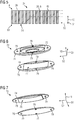
- the silicon substrate 26 filled with the tin alloy is inserted into a tool 72.
- the tool 72 is in FIG. 6, 7 shown in more detail and has an upper shell 74 and a lower shell 76.
- a lower mold surface 77 and on the upper shell 74 an upper mold surface 78 are worked out.
- the two forming surfaces 77 and 78 are curved against the same along a circular cylindrical surface.
- the lower mold surface 77 is concave in the lower shell 76 incorporated.
- the upper mold surface 78 is formed convexly protruding from the upper shell 74.
- the curvature radius of the two molding surfaces 77 and 78 is 300 millimeters.
- the filled silicon substrate 26 is thereby inserted into the tool 72 such that the first substrate direction S1 is aligned parallel to the cylinder axis of the molding surfaces 77 and 78, respectively. As a result, the bending of the silicon substrate 26 takes place about the bending axis aligned in the first substrate direction S1.
- the upper shell 74 is after clamping of the tool 72 with weights or springs so "braced" against the lower shell 76 that results in a closing force corresponding to a mass of 50 grams.
- the upper shell 74 and the lower shell 76 are made of an aluminum alloy. To close the tool 72 The upper shell 74 and the lower shell 76 are guided by means of guide pins which are inserted into corresponding holes 79 of the upper shell 74 and the lower shell 76 to each other.
- the closed mold 72 (with the filled, filled silicon substrate 26 inserted therein) is set in a furnace tempered to 200 degrees Celsius. At this temperature value (also referred to as the "working temperature value"), creep (also referred to as “retardation”) occurs below the closing force of the tool 72 in the tin alloy. Ie. The tin alloy goes through a plastic deformation despite the low closing force. Due to the above-described screening of the silicon substrate 26 with the gaps 38, the flexural rigidity of the silicon substrate 26 is so low that the silicon substrate 26 abuts the molding surfaces 77 and 78, respectively, with creeping of the tin alloy. Due to the plastic deformation of the tin alloy, the contour predetermined by the shaping surfaces 77 and 78 is retained even after the tool 72 has been opened by the silicon substrate 26 filled with the tin alloy as the final contour.
- the lamellae 6 formed by the gaps 38 filled with the tin alloy are rotationally symmetrical, so that a periodic, homogeneous X-ray absorption, which is matched to the radiation field-specifically the respective X-ray partial beam 8 -is possible.
- the intended closing forces of the tool 72 are outside a range in which the longitudinal webs 40 and / or the transverse webs 42 would be mechanically damaged.
- no compression of the lamellae 6 takes place, but only the rotationally symmetrical alignment about the first substrate direction S1.
- the latter can optionally be supported by the fact that in the edge regions 62 the longitudinal webs 40 (and thus also the transverse webs 42) protrude to the rear surface 34.
- the silicon substrate 26 is removed at least to a large extent, so that the slats 6 remain "comb-like". For example, remaining in the thickness direction 10, a remainder of the silicon substrate 26 remains, which is short in comparison to the "height" of the lamellae 6 extending in the thickness direction 10 in order to enable the geometrical cohesion of the individual lamellae 6.
- This process step takes place in particular if the partial removal in the in FIG. 5 described sub-step has not occurred. In a further exemplary embodiment, however, this method step also takes place in order to further expose the lamellae 6.
- phase contrast grating 4 formed by the slats 6 is installed in the X-ray machine 1.
Abstract
Bei einem Verfahren zur Herstellung eines Mikrostrukturbauteils (4), das insbesondere als Röntgenphasenkontrastgitter in einem Röntgengerät (1) zum Einsatz kommt, wird verfahrensgemäß in eine zumindest um eine Biegeachse deformierbare Form (26), die durch ein Siliziumsubstrat gebildet ist, und die eine Vielzahl von in einer Dickenrichtung (10) des Siliziumsubstrats (26) verlaufenden Aussparungen (38) mit Abmessungen im Mikrometerbereich aufweist, ein Röntgenstrahlen absorbierendes Material eingefüllt. Die Form (26) mit dem eingefüllten Material wird auf einen oberhalb der Raumtemperatur und unterhalb eines Schmelztemperaturwerts des eingefüllten Materials liegenden Arbeitstemperaturwert temperiert und in eine bestimmungsgemäße Endkontur verformt.In a method for producing a microstructure component (4) which is used in particular as an X-ray phase contrast grating in an X-ray machine (1) is according to the method in a deformable at least about a bending axis shape (26), which is formed by a silicon substrate, and a plurality of recesses (38) having dimensions in the micrometer range extending in a thickness direction (10) of the silicon substrate (26), an X-ray absorbing material is filled. The mold (26) with the filled material is heated to a working temperature value lying above the room temperature and below a melting temperature value of the filled material and deformed into an intended final contour.
Description
Die vorliegende Erfindung betrifft ein Verfahren zur Herstellung eines Mikrostrukturbauteils, insbesondere eines Röntgenphasenkontrastgitters. Des Weiteren betrifft die vorliegende Erfindung ein Mikrostrukturbauteil, insbesondere ein Röntgenphasenkontrastgitter sowie ein Röntgengerät mit einem solchen.The present invention relates to a method for producing a microstructure component, in particular an X-ray phase contrast grid. Furthermore, the present invention relates to a microstructure component, in particular an X-ray phase contrast grating and an X-ray apparatus with such.
Im Bereich der Röntgenbildgebung insbesondere im medizinischen Bereich, wird teilweise der sogenannte Talbot-Effekt genutzt. Hierdurch können präzisere Bildinformationen generiert werden, indem der Kontrast der erzeugten Bilder durch Einbeziehung einer von einem Untersuchungsobjekt verursachten Phasenverschiebung der Röntgenstrahlen verbessert wird. Dabei kommt regelmäßig ein sogenanntes (Röntgen-)Phasenkontrastgitter zum Einsatz, das in den Strahlengang eingebracht wird. Ein solches Gitter ist dabei üblicherweise durch in Röntgen-Strahlungsrichtung ausgerichtete Lamellen aus einem röntgenstrahlenabsorbierenden Material gebildet. Üblicherweise liegen die Wandstärke und die Abstände dieser Lamellen zueinander dabei im ein- bis gering zweistelligen Mikrometerbereich. Auch die Dicke (oder: Höhe) des gesamten Gitters liegt im durchstrahlten Bereich bei meist maximal einem Millimeter. Somit handelt es sich bei einem solchen Phasenkontrastgitter um ein Mikrostrukturbauteil.In the field of X-ray imaging, especially in the medical field, the so-called Talbot effect is used in part. As a result, more precise image information can be generated by improving the contrast of the generated images by including a phase shift of the X-rays caused by an examination subject. In this case, a so-called (X-ray) phase contrast grid is used regularly, which is introduced into the beam path. Such a grid is usually formed by aligned in the X-ray radiation direction lamellae of an X-ray absorbing material. Usually, the wall thickness and the distances between these lamellae are in the one to two-digit micrometre range. The thickness (or: height) of the entire grid is in the irradiated area usually a maximum of one millimeter. Thus, such a phase contrast grating is a microstructure component.
Aufgrund der geringen Abmessungen werden diese Phasenkontrastgitter meist durch Ätzverfahren in Siliziumwafern und nachträglichem Füllen der geätzten Vertiefungen mit Röntgenstrahlen absorbierendem Material, insbesondere einem Metall oder einer Metalllegierung, zur Ausbildung der Lamellen hergestellt. Dies ist beispielsweise aus
Der Erfindung liegt die Aufgabe zugrunde, ein verbessertes Mikrostrukturbauteil zu ermöglichen.The invention has for its object to provide an improved microstructure component.
Diese Aufgabe wird erfindungsgemäß gelöst durch ein Verfahren zur Herstellung eines solchen Mikrostrukturbauteils mit den Merkmalen des Anspruchs 1. Des Weiteren wird diese Aufgabe erfindungsgemäß gelöst durch ein Mikrostrukturbauteil mit den Merkmalen des Anspruchs 13. Außerdem wird die Aufgabe erfindungsgemäß gelöst durch ein Röntgengerät mit den Merkmalen des Anspruchs 14. Vorteilhafte und teils für sich erfinderische Ausführungsformen und Weiterbildungen der Erfindung sind in den Unteransprüchen und der nachfolgenden Beschreibung dargelegt.This object is achieved by a method for producing such a microstructure component having the features of
Das erfindungsgemäße Verfahren dient zur Herstellung eines Mikrostrukturbauteils, insbesondere eines (Röntgen-)Phasenkontrastgitters. Verfahrensgemäß wird dabei in eine zumindest um eine Biegeachse (insbesondere elastisch) deformierbare Form, die durch ein Siliziumsubstrat gebildet ist und die eine Vielzahl von in einer Dickenrichtung des Siliziumsubstrats verlaufenden Aussparungen aufweist, ein Röntgenstrahlen absorbierendes Material eingefüllt. Die Aussparungen weisen dabei Abmessungen im Mikrometerbereich auf (d. h. insbesondere in Flächenrichtung gesehen kleinste Abmessungen betragen etwa bis 10 Mikrometer, insbesondere etwa 0,5, 1 oder bis zu 4 Mikrometer). Die Form mit dem eingefüllten Material wird auf einen oberhalb der Raumtemperatur und unterhalb eines Schmelztemperaturwerts des eingefüllten Materials liegenden Arbeitstemperaturwert temperiert und anschließend in eine bestimmungsgemäße Endkontur verformt.The method according to the invention serves to produce a microstructure component, in particular an (X-ray) phase contrast grating. According to the method, an X-ray absorbing material is introduced into an at least one bending axis (in particular elastically) deformable form, which is formed by a silicon substrate and has a multiplicity of recesses extending in a thickness direction of the silicon substrate. The recesses in this case have dimensions in the micrometer range (that is, in particular in the surface direction, the smallest dimensions amount to approximately 10 micrometers, in particular approximately 0.5, 1 or up to 4 micrometers). The mold with the filled material is heated to a working temperature value lying above the room temperature and below a melting temperature value of the filled material and then deformed into a proper final contour.
Dadurch, dass die Verformung der mit dem Material gefüllten Form unterhalb der Schmelztemperatur des Materials erfolgt, wird vorteilhafterweise verhindert, dass das Material schmilzt und im schmelzflüssigen Zustand aus den Aussparungen austreten kann. Des Weiteren ist eine Füllung der Form, konkret der Aussparungen vor der Verformung in die Endkontur regelmäßig einfacher als die Füllung einer bereits vorgeformten Form.Characterized in that the deformation of the filled with the material form is below the melting temperature of the material, is advantageously prevented that the material melts and can emerge from the recesses in the molten state. Furthermore, a filling of the mold, specifically the recesses before the deformation in the final contour is usually easier than the filling of an already preformed shape.
Besonders bevorzugt wird die "gefüllte" Form, d. h. die Form mit dem eingefüllten Material bei dem Arbeitstemperaturwert unter (insbesondere temperatur-unterstütztem) Kriechen des eingefüllten Materials auf die bestimmungsgemäße Endkontur verformt. Unter Kriechen (oder auch: "Retardation") wird dabei insbesondere zumindest eine Gefügeänderung verstanden, die vergleichsweise langsam und meist unter vergleichsweise geringer Belastung abläuft und zu einer plastischen Verformung führt. Meist sind die Vorgänge, die zu einer solchen Gefügeänderung führen, thermisch aktiviert, erfolgen (insbesondere bei Metallen) also erst ab einer meist gegenüber Raumtemperatur erhöhten Temperatur. Durch die vorstehend beschriebene Ausnutzung des Kriechens des eingefüllten Materials wird vorteilhafterweise ermöglicht, die gefüllte Form mit vergleichsweise geringen Umformkräften in die Endkontur zu verformen. Dadurch kann vorteilhafterweise ein Risiko, die Mikrostrukturen des Mikrostrukturbauteils und/oder der Form zu beschädigen und somit die Genauigkeit des Mikrostrukturbauteils zu verringern, gesenkt werden.Particularly preferred is the "filled" form, i. H. deformed the mold with the filled material at the working temperature value under (in particular temperature-assisted) creep of the filled material to the intended final contour. Under creep (or "retardation") is understood in particular at least one microstructural change that runs comparatively slowly and usually under relatively low load and leads to a plastic deformation. Most of the processes that lead to such a structural change, thermally activated, done (especially in metals) so only from a temperature usually increased to room temperature. The above-described utilization of the creep of the filled material advantageously makes it possible to deform the filled mold into the final contour with comparatively low forming forces. As a result, a risk of damaging the microstructures of the microstructure component and / or the shape and thus reducing the accuracy of the microstructure component can advantageously be reduced.
Vorzugsweise wird als Röntgenstrahlen absorbierendes Material, insbesondere ein Metall (vorzugsweise mit einer vergleichsweise hohen Kriechneigung), beispielsweise Zinn oder eine Zinnlegierung herangezogen.Preferably, as the X-ray absorbing material, in particular a metal (preferably with a relatively high creep), for example, tin or a tin alloy is used.
In einer bevorzugten Verfahrensvariante wird als Arbeitstemperaturwert ein Wert von etwa 20-50 Prozent, insbesondere von etwa 30-40 Prozent des Schmelztemperaturwerts des Röntgenstrahlen absorbierenden Materials herangezogen. Insbesondere handelt es sich bei dem Arbeitstemperaturwert mindestens um den Wert einer sogenannten Übergangstemperatur, ab der Gefügemechanismen des Materials (insbesondere des Metalls) thermisch aktiviert ablaufen. Ab diesem Temperaturwert nimmt somit die Kriechneigung insbesondere metallischer Materialien zu. Regelmäßig erfolgt dabei eine plastische Deformation bereits bei in das Material eingebrachten Spannungen (Spannungswerten), die unterhalb einer Streckgrenze des Materials liegen. Besonders bevorzugt wird dabei das Röntgenstrahlen absorbierende Material, insbesondere das Metall oder eine Metalllegierung derart gewählt, dass die Deformation durch Kriechen bei einem Arbeitstemperaturwert und Spannungswerten erfolgt, die vorteilhafter Weise nicht zu einer Schädigung der Struktur der Form führen. Somit kann die Form mit dem eingefüllten Röntgenstrahlen absorbierenden Material vorteilhafterweise mit derart geringen Belastungen umgeformt werden, die bei unterhalb dem Arbeitstemperaturwert liegenden Temperaturwerten, insbesondere bei Raumtemperatur lediglich zu einer elastischen Verformung führen würden. Bei Zinn liegt der Arbeitstemperaturwert insbesondere bei etwa 200 Grad Celsius.In a preferred variant of the method, the working temperature value used is a value of about 20-50 percent, in particular about 30-40 percent, of the melting temperature value of the X-ray absorbing material. In particular, the working temperature value is at least the value of a so-called transition temperature, starting from the microstructure mechanisms of the material (in particular of the metal) run off thermally activated. From this temperature value, the creep, in particular of metallic materials, increases. In this case, a plastic deformation takes place regularly even when the stresses introduced into the material (stress values) are below a yield strength of the material. In this case, the x-ray-absorbing material, in particular the metal or a metal alloy, is particularly preferably selected such that the deformation takes place by creeping at a working temperature value and voltage values which advantageously do not lead to damage to the structure of the mold. Thus, the mold with the filled-in X-ray absorbing material can advantageously be reshaped with such low loads that would only result in elastic deformation at temperatures below the working temperature, especially at room temperature. In the case of tin, the working temperature value is in particular around 200 degrees Celsius.
In einer zweckmäßigen Verfahrensvariante wird das Röntgenstrahlen absorbierende Material in schmelzflüssigem Zustand in die Form, insbesondere in die Aussparungen eingebracht. Insbesondere kommt dabei ein Druckgussverfahren zum Einsatz. Durch das schmelzflüssige Einfüllen des Materials wird vorteilhafterweise eine mechanische Wechselwirkung zwischen der Form und dem einzufüllenden Material verringert, sodass wiederum das Risiko, die Mikrostrukturen der Form zu beschädigen, verringert wird. Insbesondere durch die Nutzung von Druck wird dabei eine möglichst vollständige Füllung der Form und somit eine präzise Abformung der Mikrostrukturen ermöglicht.In an expedient variant of the method, the x-ray absorbing material is introduced in the molten state into the mold, in particular into the recesses. In particular, a die casting method is used. The molten filling of the material advantageously reduces a mechanical interaction between the mold and the material to be filled, which in turn reduces the risk of damaging the microstructures of the mold. In particular, by the use of pressure while a complete filling of the mold and thus a precise impression of the microstructures is possible.
In einer besonders zweckmäßigen Verfahrensvariante wird das Siliziumsubstrat der Form vor dem Einbringen des Röntgenstrahlen absorbierenden Materials zur Vermeidung einer chemischen Bindung des Materials mit dem Siliziumsubstrat vorbehandelt. Beispielsweise wird das Siliziumsubstrat - vorzugsweise alle Oberflächen, die bestimmungsgemäß mit dem einzuführenden Material in Kontakt kommen - konditioniert (beispielsweise mit einer Lösung, Plasma oder dergleichen) oder beschichtet (beispielsweise mittels Sputtern, PVD, CVD oder dergleichen). Dadurch wird ermöglicht, dass die Form in einem optionalen Verfahrensschritt nach (oder alternativ auch vor) dem Umformen zumindest teilweise entfernt werden kann, sodass das in die Aussparungen eingefüllte Material beispielsweise als Säule, Lamelle oder dergleichen zumindest zum Großteil vereinzelt stehen bleibt.In a particularly expedient process variant, the silicon substrate of the mold is pretreated prior to introduction of the X-ray absorbing material to avoid chemical bonding of the material to the silicon substrate. For example, the silicon substrate - preferably all surfaces that are intended to be introduced with the Material come into contact - conditioned (for example with a solution, plasma or the like) or coated (for example by means of sputtering, PVD, CVD or the like). This makes it possible that the mold can be at least partially removed in an optional process step after (or alternatively before) forming, so that the material filled into the recesses, for example as column, lamella or the like, at least for the most part remains isolated.
In einer weiteren zweckmäßigen Verfahrensvariante wird die Form mit dem eingefüllten Material mittels eines Werkzeugs verformt, das eine Unterschale und eine Oberschale mit jeweils gegengleich entlang einer Kreiszylinderfläche gewölbten Formflächen aufweist (die Formflächen sind also jeweils in die gleiche Richtung gewölbt und verlaufen im bestimmungsgemäßen Einsatzzustand somit parallel zueinander). Insbesondere wird die gefüllte Form zwischen die Unterschale und die Oberschale eingelegt und die Oberschale anschließend mit einer zur "Kriech-Umformung" erforderlichen Kraft belastet.In a further expedient variant of the method, the mold is deformed with the filled-in material by means of a tool which has a lower shell and an upper shell with respective curved surfaces along a circular cylindrical surface (the mold surfaces are thus arched in the same direction and thus run parallel in the intended operating condition to each other). In particular, the filled mold is inserted between the lower shell and the upper shell and then the upper shell is loaded with a force required for "creep-forming".
Vorzugsweise wird zur Verformung insbesondere mittels der vorstehend beschriebenen Oberschale eine Kraft (auch als "Schließkraft" bezeichnet) auf die Form ausgeübt, die insbesondere einer Masse von 10-150 Gramm, vorzugsweise von 20-100 Gramm entspricht. Eine solche Kraft ist insbesondere bei Abmessungen des Mikrostrukturbauteils in Dickenrichtung von kleiner als ein Millimeter, insbesondere im Bereich bis etwa 500 Mikrometer zur Kriech-Umformung unter Vermeidung von Beschädigungen der Mikrostrukturen der Form ausreichend.Preferably, for the deformation, in particular by means of the above-described upper shell, a force (also referred to as "closing force") is exerted on the mold, which in particular corresponds to a mass of 10-150 grams, preferably 20-100 grams. Such a force is sufficient in particular for dimensions of the microstructure component in the thickness direction of less than one millimeter, in particular in the range up to about 500 microns for creep deformation while avoiding damage to the microstructures of the mold.
In einer fertigungstechnisch zweckmäßigen Verfahrensvariante wird die Verformung der gefüllten Form in einem Ofen, insbesondere einem Umluftofen, durchgeführt, in dem die Temperierung auf den Arbeitstemperaturwert stattfindet. Vorzugsweise wird dabei die gefüllte Form in das vorstehend beschriebene Werkzeug eingelegt, mit der entsprechenden Kraft belastet und anschließend in den Ofen eingestellt. In dem Ofen erwärmen sich das Werkzeug und somit auch die eingelegte Form auf den Arbeitstemperaturwert, sodass aufgrund der aufgebrachten Kraft das Röntgenstrahlen absorbierende Material sich durch Kriechen insbesondere auf die durch das Werkzeug vorgegebene Endkontur verformt. Vorzugsweise ist die Form dabei derart elastisch ausgebildet, dass sie der Verformung des eingefüllten Materials elastisch folgt. Durch das Kriechen des eingefüllten Materials findet aber eine plastische Verformung des Materials statt, wodurch auch die Form selbst nach dem Entformen aus dem Werkzeug die erreichte Endkontur beibehält.In a production-technically expedient method variant, the deformation of the filled mold is carried out in an oven, in particular a forced-air oven, in which the temperature control takes place at the working temperature value. Preferably, the filled mold is inserted into the tool described above, loaded with the appropriate force and then set in the oven. Heat in the oven the tool and thus also the inserted shape to the working temperature value, so that due to the applied force, the X-ray absorbing material is deformed by creeping, in particular to the predetermined by the tool final contour. In this case, the mold is preferably designed so elastically that it elastically follows the deformation of the filled material. Due to the creeping of the filled material, however, a plastic deformation of the material takes place, as a result of which the shape, even after removal from the mold, retains the final contour reached.
In einer bevorzugten Verfahrensvariante werden die Aussparungen der Form durch eine ätztechnische Ausbildung von Spalten gebildet. Diese Spalte verlaufen dabei in einer ersten Substratrichtung und sind durch Querstege, die in einer zur ersten Substratrichtung senkrecht stehenden zweiten Substratrichtung verlaufen, voneinander getrennt. Außerdem sind die Spalte auch zeilenartig in der zweiten Substratrichtung nebeneinander angeordnet, wobei die einzelnen Zeilen durch parallel zu den Spalten verlaufende Längsstege voneinander getrennt sind. D. h. die Spalte sind in einem Raster angeordnet, in dem innerhalb der Zeilen die Spalte mit ihrer Längsrichtung parallel zur ersten Substratrichtung stehen und in der zweiten Substratrichtung mehrere Zeilen (insbesondere mit jeweils mehreren Spalten) nebeneinander angeordnet sind. Vorzugsweise ist dabei das gesamte Siliziumsubstrat zumindest in der ersten Substratrichtung von dem Raster abgedeckt. Aufgrund dieser Ausrichtung der Spalte wird eine Biegesteifigkeit des Siliziumsubstrats (und somit der Form) um eine in der ersten Substratrichtung ausgerichtete Biegeachse vorteilhaft verringert. Vorzugsweise erfolgt die Umformung der (gefüllten) Form auch um diese Biegeachse.In a preferred variant of the method, the recesses of the mold are formed by an etching-technical formation of gaps. In this case, these gaps run in a first substrate direction and are separated from one another by transverse webs which run in a second substrate direction perpendicular to the first substrate direction. In addition, the gaps are also arranged in rows in the second substrate direction next to each other, wherein the individual rows are separated by parallel to the columns extending longitudinal ridges. Ie. the gaps are arranged in a grid in which, within the rows, the gaps are parallel to the first substrate direction with their longitudinal direction and a plurality of rows (in particular with a plurality of columns in each case) are arranged next to one another in the second substrate direction. Preferably, the entire silicon substrate is covered by the grid at least in the first substrate direction. Due to this alignment of the column, a flexural rigidity of the silicon substrate (and thus of the mold) is advantageously reduced by a bending axis aligned in the first substrate direction. Preferably, the forming of the (filled) shape also takes place about this bending axis.
In einer besonders zweckmäßigen Weiterbildung sind die vorstehend beschriebenen Spalte, die in der zweiten Substratrichtung aufeinanderfolgen, bezüglich ihrer Längserstreckung entlang der ersten Substratrichtung zueinander versetzt angeordnet. D. h. die Spalte sind von Zeile zu Zeile in der ersten Substratrichtung verschoben. Vorzugsweise sind die Spalte dabei um die Hälfte ihrer bestimmungsgemäßen Längserstreckung verschoben. Dadurch ergibt sich, dass die vorstehend beschriebenen Querstege in der zweiten Substratrichtung gesehen nur in jeder zweiten Zeile miteinander fluchten. Außerdem ergibt sich durch die Verschiebung um die halbe Längserstreckung eine gleichmäßige und insbesondere symmetrische Deformation bei einer Biegung um die vorstehend beschriebene Biegeachse.In a particularly expedient refinement, the gaps described above, which follow one another in the second substrate direction, are offset relative to one another with respect to their longitudinal extension along the first substrate direction. Ie. the columns are from row to row in the first one Substrate direction shifted. Preferably, the gaps are shifted by half of their intended longitudinal extent. This results in that the transverse webs described above in the second substrate direction are aligned with each other only in every second row. In addition, the displacement by half the longitudinal extent results in a uniform and, in particular, symmetrical deformation in the case of a bend about the bending axis described above.
In einer weiteren zweckmäßigen Verfahrensvariante werden die Aussparungen, insbesondere die vorstehend beschriebenen Spalte insbesondere mittels anisotroper Ätzverfahren derart ausgeformt, dass sie das Siliziumsubstrat in Dickenrichtung durchdringen. Mithin sind die Aussparungen bzw. Spalte vorzugsweise beidseitig zu dem Siliziumsubstrat geöffnet.In a further expedient variant of the method, the recesses, in particular the gaps described above, are formed in particular by means of anisotropic etching processes in such a way that they penetrate the silicon substrate in the thickness direction. Thus, the recesses or gaps are preferably open on both sides of the silicon substrate.
Vorzugsweise wird zur Ausbildung der Form in eine erste Oberfläche des insbesondere scheibenartigen Siliziumsubstrats (bspw. in einen Wafer oder einen Teil eines Wafers) insbesondere ätztechnisch eine Vielzahl von punktartigen (vorzugsweise pyramidenförmigen) und insbesondere voneinander separaten Impfstrukturen in dem vorstehend beschriebenen Raster eingebracht. Die Impfstrukturen werden dabei in der ersten Substratrichtung in Gruppen zusammengefasst, die der jeweiligen Aussparung, vorzugsweise einem jeden Spalt zugeordnet sind. Die Gruppen sind in der ersten Substratrichtung voneinander zur späteren Ausbildung der Querstege beabstandet. Darauf folgend werden die Impfstrukturen in Tiefenrichtung (oder auch: Dickenrichtung) des Siliziumsubstrats in einem Ätzschritt zu Bohrlöchern verlängert - d. h. vertieft. Anschließend wird eine der ersten Oberfläche des Siliziumsubstrats gegenüberliegende zweite Oberfläche zur rückseitigen Öffnung der Bohrlöcher in einem weiteren Ätzschritt zumindest teilweise entfernt. In einem nachfolgenden Ätzschritt wird dann ein anisotrop wirksames Ätzmedium - insbesondere eine Ätzlösung - alternierend von beiden Oberflächen des Siliziumsubstrats her durch die Bohrlöcher gespült, so dass sich die (insbesondere zunächst runden) Bohrlöcher (vorzugsweise zu einem quadratischen Querschnitt) aufweiten und sich innerhalb der jeweiligen Gruppe zu der jeweiligen Aussparung, insbesondere zu dem in der ersten Substratrichtung verlaufenden Spalt verbinden. Vorzugsweise wird die erste Oberfläche des Siliziumsubstrats dabei derart gewählt, dass sie parallel zu einer "(100)-Kristallebene" des Siliziums ausgerichtet ist.Preferably, in order to form the mold into a first surface of the particular disk-like silicon substrate (for example into a wafer or a part of a wafer), a plurality of punctiform (preferably pyramidal) and in particular separate from each other vaccination structures in the grid described above is introduced. In this case, the seed structures are combined in groups in the first substrate direction, which groups are assigned to the respective recess, preferably to each gap. The groups are spaced from each other in the first substrate direction for later formation of the transverse webs. Subsequently, the seed structures in the depth direction (or thickness direction) of the silicon substrate are extended to drill holes in one etching step - that is, deepened. Subsequently, a second surface opposite the first surface of the silicon substrate for rear opening of the boreholes is at least partially removed in a further etching step. In a subsequent etching step, an anisotropically effective etching medium-in particular an etching solution-is then rinsed alternately from both surfaces of the silicon substrate through the drilled holes, so that the (Especially initially round) bore holes (preferably to a square cross-section) expand and connect within the respective group to the respective recess, in particular to the gap extending in the first substrate direction. Preferably, the first surface of the silicon substrate is chosen such that it is aligned parallel to a "(100) crystal plane" of the silicon.
In einer bevorzugten Verfahrensvariante werden die Aussparungen, insbesondere die Spalte mit einem Aspektverhältnis in Dickenrichtung des Siliziumsubstrats von etwa 1:450 ausgeformt. Die Aussparungen bzw. Spalte weisen dabei insbesondere in der zweiten Substratrichtung gesehen Abmessungen (d. h. eine Breite) von etwa ein bis vier Mikrometern auf. Derart "feine" (d. h. kleine und filigrane) Strukturen sind insbesondere für den Einsatz des Mikrostrukturbauteils als (Röntgen-) Phasenkontrastgitter in einem Röntgengerät vorteilhaft. Die zur Absorption von Röntgenstrahlen dienenden Lamellen dieses Phasenkontrastgitters werden dabei durch das Röntgenstrahlen absorbierende und in die Aussparungen eingefüllte Material gebildet. Vorzugsweise liegen die vorstehend beschriebenen, durch die in der ersten Substratrichtung verlaufenden Spalte gebildeten Zeilen dabei mit einem Abstand von etwa 2-12 Mikrometern auseinander. Dies entspricht insbesondere einer sogenannten Gitterkonstanten des Phasenkontrastgitters.In a preferred variant of the method, the recesses, in particular the gaps, have an aspect ratio in the thickness direction of the silicon substrate of approximately 1: 450. The recesses or gaps in this case, in particular in the second substrate direction, have dimensions (that is to say a width) of approximately one to four micrometers. Such "fine" (i.e., small and filigree) structures are particularly advantageous for use of the microstructure component as (X-ray) phase contrast gratings in an X-ray machine. The lamellae of this phase-contrast lattice used for the absorption of X-rays are formed by the material which absorbs X-rays and is filled into the recesses. Preferably, the above-described lines formed by the gaps extending in the first substrate direction are spaced apart by a distance of approximately 2-12 micrometers. This corresponds in particular to a so-called lattice constant of the phase contrast grating.
Weiter vorzugsweise werden die vorstehend beschriebenen Spalte mit einer Längserstreckung zwischen 20 und 1300, vorzugsweise zwischen 50 und weniger als 1000 Mikrometern ausgebildet. Insbesondere bei Werten unter 1000 (insbesondere bis zu 300) Mikrometern ergeben sich einerseits eine zur Umformung der gefüllten Form hinreichend geringe aber zur Handhabung (auch der gefüllten Form) ausreichend hohe Biegesteifigkeit insbesondere um eine in der ersten Substratrichtung liegende Biegeachse.Further preferably, the gaps described above are formed with a longitudinal extent between 20 and 1300, preferably between 50 and less than 1000 micrometers. Particularly at values below 1000 (in particular up to 300) micrometers, on the one hand, a bending stiffness sufficiently low for shaping the filled mold but sufficiently high for handling (even the filled mold) results, in particular, around a bending axis lying in the first substrate direction.
Um die Biegesteifigkeit der gefüllten Form für das Umformen um diese Biegeachse weiter zu senken, wird in einem optionalen Verfahrensschritt vor dem Umformen in einem (weiteren) Ätzschritt ein zentraler Bereich der Rückseite (d. h. der zweiten Oberfläche) des Siliziumsubstrats bis auf eine Restdicke entfernt und nur in der zweiten Substratrichtung endständige Randbereiche des Siliziumsubstrats belassen. In dem zentralen Bereich stehen dabei - wie vorstehend beschrieben - die durch das eingefüllte Material gebildeten Säulen oder Lamellen aus dem Siliziumsubstrat vor. Insbesondere für den Einsatz des Mikrostrukturbauteils als Phasenkontrastgitter wird in dem zentralen Bereich (der vorzugsweise einem durchstrahlten Bereich entspricht) dadurch auch eine Absorption der Röntgenstrahlen im Silizium verringert.In order to further reduce the bending stiffness of the filled mold for forming around this bending axis, in an optional process step before forming in a (further) etching step, a central region of the back side (ie the second surface) of the silicon substrate is removed to a residual thickness and only leave in the second direction substrate terminal edge regions of the silicon substrate. In the central region, as described above, the columns or lamellae formed by the filled material protrude from the silicon substrate. In particular for the use of the microstructure component as a phase contrast grating, an absorption of the X-rays in the silicon is thereby also reduced in the central region (which preferably corresponds to an irradiated region).
Das erfindungsgemäße Mikrostrukturbauteil stellt insbesondere das vorstehend genannte Phasenkontrastgitter dar und ist gemäß dem vorstehend beschriebenen Verfahren hergestellt. D. h. das Mikrostrukturbauteil weist ebenfalls die vorstehend beschriebenen, insbesondere sich aus dem Herstellungsverfahren ergebenden körperlichen Merkmale und Vorteile auf.The microstructure component according to the invention is in particular the above-mentioned phase contrast grating and is produced according to the method described above. Ie. The microstructure component likewise has the physical features and advantages described above, in particular resulting from the production method.
Das erfindungsgemäße Röntgengerät weist das durch das vorstehend beschriebene Mikrostrukturbauteil gebildete Phasenkontrastgitter auf, und teilt somit ebenfalls die vorstehend beschriebenen Merkmale und Vorteile.The X-ray apparatus according to the invention has the phase contrast grating formed by the above-described microstructure component, and thus also shares the features and advantages described above.
Nachfolgend werden Ausführungsbeispiele der Erfindung anhand einer Zeichnung näher dargestellt. Darin zeigen:
- FIG 1
- in einer schematischen Seitenansicht ein Röntgengerät mit einem Phasenkontrastgitter,
- FIG 2
- in einem schematischen Ablaufdiagramm ein Verfahren zur Herstellung des Phasenkontrastgitters,
- FIG 3
- in einer schematischen Draufsicht ein Raster von Impfstrukturen zur Erzeugung des Phasenkontrastgitters aus einem Siliziumsubstrat,
- FIG 4
- in Ansicht gemäß
FIG 3 aus dem Raster gebildete Spalte in dem Siliziumsubstrat, - FIG 5
- in einer schematischen Schnittansicht das Phasenkontrastgitter in einem Fertigungszwischenschritt, und
- FIG 6,7
- in jeweils unterschiedlichen schematischen Perspektivansichten ein Werkzeug zur Umformung des Phasenkontrastgitters auf eine Endkontur.
- FIG. 1
- in a schematic side view of an X-ray machine with a phase contrast grid,
- FIG. 2
- in a schematic flow diagram, a method for producing the phase contrast grating,
- FIG. 3
- in a schematic plan view, a grid of Impfstrukturen for generating the phase contrast grid of a silicon substrate,
- FIG. 4
- in view according to
FIG. 3 column formed in the grid in the silicon substrate, - FIG. 5
- in a schematic sectional view of the phase contrast grid in an intermediate manufacturing step, and
- 6,7
- in each case different schematic perspective views of a tool for forming the phase contrast grating on a final contour.
Einander entsprechende Teile sind in allen Figuren stets mit gleichen Bezugszeichen versehenCorresponding parts are always provided with the same reference numerals in all figures
In
In einem ersten Verfahrensschritt 20 werden dabei Impfstrukturen 22 (s.
Die Impfstrukturen 22 sind dabei quadratisch mit einer Kantenlänge von kleiner oder gleich 2 Mikrometern ausgebildet. Eine Längserstreckung LG der Gruppen 32 beträgt somit etwa 50 Mikrometer.The seed structures 22 are square with an edge length of less than or equal to 2 microns. A longitudinal extent LG of the
Die Gruppen 32 sind außerdem mit einem dritten Abstand A3 zueinander beanstandet angeordnet. Der dritte Abstand A3 entspricht dabei etwa einer Auslassung einer der Impfstrukturen 22 in der jeweiligen Zeile 30.The
Die Impfstrukturen 22 werden anschließend in Dickenrichtung 10 mittels eines Ätzverfahrens zu Bohrlöchern erweitert, deren Seitenwände senkrecht zu der ersten Oberfläche 24 stehen. Dazu wird das sogenannte PAECE-Verfahren ("photo assisted electro-chemical etching") eingesetzt. Konkret werden die Impfstrukturen 22 zu kreiszylindrischen Bohrlöchern mit einer Tiefe von 470 Mikrometern erweitert.The seed structures 22 are then expanded in the
Die der ersten Oberfläche 24 gegenüberliegende zweite Oberfläche 34 wird anschließend derart entfernt, dass die Bohrlöcher rückseitig (d. h. zu der zweiten Oberfläche 34 hin) geöffnet sind. Dazu kommen Ätzverfahren wie zum Beispiel nasschemisches Ätzen mit Kaliumhydroxid oder plasmainduziertes Trockenätzen zum Einsatz. In einem im bestimmungsgemäßen Einsatzzustand im Röntgengerät 1 von den Röntgen-Teilstrahlen 8 durchstrahlten Bereich beträgt die Dicke des Siliziumsubstrats 26 anschließend 450 Mikrometer.The
In einem weiteren Ätzschritt werden die Bohrlöcher alternierend von der ersten Oberfläche 24 und der zweiten Oberfläche 34 her mit einem anisotrop wirksamen Ätzmedium durchspült. Das Ätzmedium enthält dabei Kaliumhydroxid, Wasserstoffperoxid und Isopropanol. Die erste und die zweite Substratrichtung S1 bzw. S2 sind parallel zu Richtungen gewählt, in denen (111)-Kristallebenen des Siliziums durch die (parallel zur ersten Oberfläche 24 liegenden) (100)-Kristallebene hindurch treten. Dadurch werden die einzelnen Bohrlöcher in der ersten und zweiten Substratrichtung S1 und S2 aufgeweitet, so dass sie einen quadratischen Querschnitt aufweisen, und vereinigen sich bei fortschreitender Aufweitung mit den benachbarten Bohrlöchern innerhalb der jeweiligen Gruppen 32 zu jeweils einem Spalt 38 (s.
Das Raster 28 ist dabei derart gewählt, dass die gebildeten Spalte 38 zweier direkt benachbarter Zeilen 30 um die Hälfte ihrer Längserstreckung LS in der ersten Substratrichtung S1 versetzt sind. Dadurch fluchten die Querstege 42 zweier direkt benachbarter Zeilen 30 nicht miteinander. Vielmehr fluchten die Querstege 42 immer der "übernächsten" Zeilen 30 miteinander. Dadurch ergibt sich ein guter Kompromiss von mechanischer Stabilität gegen eine Biegung um eine in der ersten Substratrichtung S1 gerichtete Biegeachse und einer hinreichenden Flexibilität für eine solche Biegung.The
In einem zweiten Verfahrensschritt 50 wird das Siliziumsubstrat 26, konkret die Oberflächen 24 und 34 sowie die Innenwände der Spalte 38 vorbehandelt, um eine chemische Bindung eines in einem nachfolgenden Verfahrensschritt 60 in die Spalte 38 einzufüllenden Röntgenstrahlen absorbierenden Materials, konkret einer Zinnlegierung, mit den Innenwänden und den Oberflächen 24 bzw. 34 zu verhindern.In a
In dem Verfahrensschritt 60 wird dazu nachfolgend mittels eines Druckgussverfahrens die Zinnlegierung in die Spalte 38 zur Ausbildung der Lamellen 6 eingefüllt. Das Siliziumsubstrat 26 bildet somit eine Form, in die die Zinnlegierung eingebracht wird.In the
Wie aus
Optional erfolgt im Rahmen des Verfahrensschritts 60 auch ein Zuschnitt des Siliziumsubstrats 26 auf die für das Röntgengerät 1 erforderlichen Abmessungen (nicht näher dargestellt, optional vor der Ausbildung der Randbereiche 62). Dabei werden die erste und die zweite Substratrichtung S1 bzw. S2 berücksichtigt und gegebenenfalls Markierungen zur Justierung aufgebracht. Der Zuschnitt wird bspw. mittels Laserstrahlschneiden oder Wafersägen durchgeführt.Optionally, as part of the
In einem weiteren Verfahrensschritt 70 wird das mit der Zinnlegierung gefüllte Siliziumsubstrat 26 in ein Werkzeug 72 eingelegt. Das Werkzeug 72 ist in
Die Oberschale 74 wird nach dem Schließen des Werkzeugs 72 mit Gewichtsstücken oder Federn derart gegen die Unterschale 76 "verspannt", dass sich eine Schließkraft, die einer Masse von 50 Gramm entspricht, ergibt.The
Die Oberschale 74 und die Unterschale 76 sind aus einer Aluminiumlegierung gefertigt. Zum Schließen des Werkzeugs 72 werden die Oberschale 74 und die Unterschale 76 mittels Führungsstiften, die in korrespondierende Bohrungen 79 der Oberschale 74 und der Unterschale 76 eingesetzt werden, zueinander geführt.The
In einem nachfolgenden Verfahrensschritt 80 wird das geschlossene Werkzeug 72 (mit dem darin eingelegten, gefüllten Siliziumsubstrat 26) in einen auf 200 Grad Celsius temperierten Ofen eingestellt. Bei diesem Temperaturwert (auch als "Arbeitstemperaturwert" bezeichnet) tritt unter der Schließkraft des Werkzeugs 72 in der Zinnlegierung Kriechen (auch als "Retardation" bezeichnet) auf. D. h. die Zinnlegierung durchläuft trotz der geringen Schließkraft eine plastische Verformung. Aufgrund der vorstehend beschriebenen Rasterung des Siliziumsubstrats 26 mit den Spalten 38 ist die Biegesteifigkeit des Siliziumsubstrats 26 derart gering, dass sich das Siliziumsubstrat 26 unter Kriechen der Zinnlegierung an die Formflächen 77 bzw. 78 anlegt. Aufgrund der plastischen Verformung der Zinnlegierung wird die durch die Formflächen 77 bzw. 78 vorgegebene Kontur auch nach Öffnen des Werkzeugs 72 von dem mit der Zinnlegierung gefüllten Siliziumsubstrat 26 als Endkontur beibehalten.In a
Durch die vorstehend beschriebene Verformung sind die durch die mit der Zinnlegierung gefüllten Spalte 38 gebildeten Lamellen 6 rotationssymmetrisch ausgerichtet, sodass eine periodische, homogene Röntgenabsorption, die dem Strahlungsfeld - konkret dem jeweiligen Röntgen-Teilstrahl 8 - angeglichen ist, möglich ist. Außerdem liegen die bestimmungsgemäßen Schließkräfte des Werkzeugs 72 außerhalb eines Bereichs, in dem die Längsstege 40 und/oder die Querstege 42 mechanisch geschädigt werden würden. Somit erfolgt bei der vorstehend beschriebenen Kriech-Umformung keine Kompression der Lamellen 6 sondern nur die rotationssymmetrische Ausrichtung um die erste Substratrichtung S1. Letzteres kann optional dadurch unterstützt werden, dass in den Randbereichen 62 die Längsstege 40 (und somit auch die Querstege 42) bis zur rückseitigen Oberfläche 34 vorstehen.As a result of the above-described deformation, the
In einem optionalen, nicht näher dargestellten weiteren Verfahrensschritt wird das Siliziumsubstrat 26 zumindest zu einem Großteil entfernt, sodass die Lamellen 6 "kammartig" stehen bleiben. Beispielsweise verbleibt in Dickenrichtung 10 gesehen ein Rest des Siliziumsubstrats 26, der im Vergleich zur in Dickenrichtung 10 verlaufenden "Höhe" der Lamellen 6 kurz ist, um den geometrischen Zusammenhalt der vereinzelten Lamellen 6 zu ermöglichen. Dieser Verfahrensschritt erfolgt insbesondere, wenn die teilweise Entfernung in dem in
Abschließend wird das durch die Lamellen 6 gebildete Phasenkontrastgitter 4 in das Röntgengerät 1 eingebaut.Finally, the phase contrast grating 4 formed by the
Der Gegenstand der Erfindung ist nicht auf die vorstehend beschriebenen Ausführungsbeispiele beschränkt. Vielmehr können weitere Ausführungsformen der Erfindung von dem Fachmann aus der vorstehenden Beschreibung abgeleitet werden. Insbesondere können die anhand der verschiedenen Ausführungsbeispiele beschriebenen Einzelmerkmale der Erfindung und deren Ausgestaltungsvarianten auch in anderer Weise miteinander kombiniert werden.The object of the invention is not limited to the embodiments described above. Rather, other embodiments of the invention may be derived by those skilled in the art from the foregoing description. In particular, the individual features of the invention described with reference to the various exemplary embodiments and their design variants can also be combined with one another in a different manner.
Claims (14)
wobei die Form (26) unter Kriechen des eingefüllten Materials in die bestimmungsgemäße Endkontur verformt wird.Method according to claim 1,
wherein the mold (26) is deformed while creeping the filled material into the intended final contour.
wobei als Arbeitstemperaturwert ein Wert von etwa 20 bis 50 Prozent, insbesondere von etwa 30 bis 40 Prozent des Schmelztemperaturwerts herangezogen wird.Method according to claim 1 or 2,
wherein a value of about 20 to 50 percent, in particular of about 30 to 40 percent of the melting temperature value is used as the working temperature value.
wobei das Röntgenstrahlen absorbierende Material in schmelzflüssigem Zustand in die Form, insbesondere die Aussparungen (38) eingebracht wird.Method according to one of claims 1 to 3,
wherein the X-ray absorbing material is introduced in a molten state into the mold, in particular the recesses (38).
wobei die Form (26) vor dem Einbringen des Röntgenstrahlen absorbierenden Materials zur Vermeidung einer chemischen Bindung des Röntgenstrahlen absorbierenden Materials mit dem die Form bildenden Siliziumsubstrat (26) vorbehandelt wird.Method according to one of claims 1 to 4,
wherein the mold (26) is pretreated prior to introducing the X-ray absorbing material to prevent chemical bonding of the X-ray absorbing material to the mold forming silicon substrate (26).
wobei die Form (26) mit dem eingefüllten Material mittels eines Werkzeugs (72), das eine Unterschale (76) und eine Oberschale (74) mit jeweils gegengleich entlang einer Kreiszylinderfläche gewölbten Formflächen (77,78) aufweist, verformt wird.Method according to one of claims 1 to 5,
wherein the mold (26) is deformed with the filled material by means of a tool (72) having a lower shell (76) and an upper shell (74) each with counter-curved surfaces (77,78) along a circular cylindrical surface.
wobei zur Verformung eine einer Masse von 10 bis 150 Gramm entsprechende Kraft auf die Form (26) ausgeübt wird.Method according to one of claims 1 to 6,
wherein a deformation of a mass of 10 to 150 grams corresponding force is applied to the mold (26) for deformation.
wobei die Verformung in einem Ofen unter Temperierung auf den Arbeitstemperaturwert durchgeführt wird.Method according to one of claims 1 to 7,
wherein the deformation is carried out in an oven under temperature to the working temperature value.
wobei die Aussparungen der Form (26) durch ätztechnische Ausbildung von Spalten (38), die in einer ersten Substratrichtung (S1) verlaufen und durch Querstege (42) voneinander getrennt und die zeilenartig parallel zueinander in einer zweiten, zur ersten Substratrichtung (S1) senkrecht stehenden Substratrichtung (S2) angeordnet sind, gebildet werden.Method according to one of claims 1 to 8,
wherein the recesses of the mold (26) by etching formation of columns (38) extending in a first substrate direction (S1) and separated by transverse webs (42) and the line-like parallel to each other in a second, to the first substrate direction (S1) perpendicular standing substrate direction (S2) are arranged are formed.
wobei die Spalte (38), die in der zweiten Substratrichtung (S2) aufeinander folgen, bezüglich ihrer Längserstreckung (LS) entlang der ersten Substratrichtung (S1) zueinander versetzt angeordnet werden.Method according to claim 9,
wherein the gaps (38) which follow one another in the second substrate direction (S2) are offset relative to one another with respect to their longitudinal extent (LS) along the first substrate direction (S1).
wobei die Aussparungen (38) derart ausgeformt werden, dass sie das Siliziumsubstrat (26) in Dickenrichtung (10) durchdringen.Method according to one of claims 1 to 10,
wherein the recesses (38) are formed so as to penetrate the silicon substrate (26) in the thickness direction (10).
wobei die Aussparungen (38) ein Aspektverhältnis in Dickenrichtung (10) von etwa 1:450 aufweisen, und wobei die Aussparungen (38) eine Breite von 1 bis 4 Mikrometern aufweisen.Method according to one of claims 1 to 11,
wherein the recesses (38) have an aspect ratio in the thickness direction (10) of about 1: 450, and wherein the recesses (38) have a width of 1 to 4 microns.
Priority Applications (3)
| Application Number | Priority Date | Filing Date | Title |
|---|---|---|---|
| EP18159242.9A EP3534376A1 (en) | 2018-02-28 | 2018-02-28 | Method for producing a microstructure component, microstructure component and xray device |
| US16/281,189 US11039802B2 (en) | 2018-02-28 | 2019-02-21 | Method for producing a microstructure component, microstructure component and x-ray device |
| CN201910149756.5A CN110211722A (en) | 2018-02-28 | 2019-02-28 | For manufacturing the method, microstructure elements and X-ray equipment of microstructure elements |
Applications Claiming Priority (1)
| Application Number | Priority Date | Filing Date | Title |
|---|---|---|---|
| EP18159242.9A EP3534376A1 (en) | 2018-02-28 | 2018-02-28 | Method for producing a microstructure component, microstructure component and xray device |
Publications (1)
| Publication Number | Publication Date |
|---|---|
| EP3534376A1 true EP3534376A1 (en) | 2019-09-04 |
Family
ID=61526641
Family Applications (1)
| Application Number | Title | Priority Date | Filing Date |
|---|---|---|---|
| EP18159242.9A Pending EP3534376A1 (en) | 2018-02-28 | 2018-02-28 | Method for producing a microstructure component, microstructure component and xray device |
Country Status (3)
| Country | Link |
|---|---|
| US (1) | US11039802B2 (en) |
| EP (1) | EP3534376A1 (en) |
| CN (1) | CN110211722A (en) |
Families Citing this family (1)
| Publication number | Priority date | Publication date | Assignee | Title |
|---|---|---|---|---|
| EP3498170A1 (en) * | 2017-12-12 | 2019-06-19 | Koninklijke Philips N.V. | Device and method for aligning an x-ray grating to an x-ray radiation source, and x-ray image acquisition system |
Citations (3)
| Publication number | Priority date | Publication date | Assignee | Title |
|---|---|---|---|---|
| JP2015121639A (en) * | 2013-12-24 | 2015-07-02 | コニカミノルタ株式会社 | Lattice curvature method, curved lattice, and x-ray imaging device |
| DE102015201741A1 (en) | 2015-02-02 | 2016-08-04 | Siemens Healthcare Gmbh | Phase contrast grating and method for producing a phase contrast grating |
| EP3054455A1 (en) * | 2013-10-25 | 2016-08-10 | Konica Minolta, Inc. | Curved grating manufacturing method, curved grating, grating unit, and x-ray imaging device |
Family Cites Families (15)
| Publication number | Priority date | Publication date | Assignee | Title |
|---|---|---|---|---|
| JP3627856B2 (en) | 2000-11-22 | 2005-03-09 | 株式会社フジクラ | Metal filling apparatus and metal filling method for fine space |
| JP3599325B2 (en) | 2001-02-09 | 2004-12-08 | 株式会社フジクラ | Method of forming through electrode on substrate and substrate having through electrode |
| DE102009019595B4 (en) | 2009-04-30 | 2013-02-28 | Forschungszentrum Karlsruhe Gmbh | High aspect ratio grating, particularly for use as an X-ray optical grating in a CT system manufactured by a lithographic process |
| US8999435B2 (en) * | 2009-08-31 | 2015-04-07 | Canon Kabushiki Kaisha | Process of producing grating for X-ray image pickup apparatus |
| JP5586986B2 (en) | 2010-02-23 | 2014-09-10 | キヤノン株式会社 | X-ray imaging device |
| CN101813796B (en) | 2010-02-26 | 2012-07-18 | 深圳大学 | Production method of silicon-substrate X-ray phase grating and production device thereof |
| DE102010017425A1 (en) | 2010-06-17 | 2011-12-22 | Karlsruher Institut für Technologie | Inclined phase lattice structures |
| JP5875280B2 (en) | 2010-10-20 | 2016-03-02 | キヤノン株式会社 | Imaging device using Talbot interference and method for adjusting imaging device |
| DE102010061481A1 (en) | 2010-12-22 | 2012-06-28 | mircoworks GmbH | Grill for use in X-ray-based system of medical device and in medical radiography system, has primary structure, which is inserted in carrier by directed etching tread and material |
| JP2012132793A (en) | 2010-12-22 | 2012-07-12 | Fujifilm Corp | Grid for taking radiation image, manufacturing method for the same and radiation image taking system |
| JP5804726B2 (en) | 2011-02-24 | 2015-11-04 | キヤノン株式会社 | Manufacturing method of fine structure |
| JP6245794B2 (en) * | 2011-07-29 | 2017-12-13 | キヤノン株式会社 | Manufacturing method of shielding grid |
| US20130164457A1 (en) * | 2011-12-27 | 2013-06-27 | Rigaku Innovative Technologies, Inc. | Method of manufacturing patterned x-ray optical elements |
| WO2017036729A1 (en) | 2015-09-01 | 2017-03-09 | Paul Scherrer Institut | Method for fabricating high aspect ratio gratings for phase contrast imaging |
| DE102016200440A1 (en) * | 2016-01-15 | 2017-07-20 | Siemens Healthcare Gmbh | Device and X-ray phase contrast imaging device with a curved interference grating and method for bending an interference grating for interferometric X-ray imaging |
-
2018
- 2018-02-28 EP EP18159242.9A patent/EP3534376A1/en active Pending
-
2019
- 2019-02-21 US US16/281,189 patent/US11039802B2/en active Active
- 2019-02-28 CN CN201910149756.5A patent/CN110211722A/en active Pending
Patent Citations (3)
| Publication number | Priority date | Publication date | Assignee | Title |
|---|---|---|---|---|
| EP3054455A1 (en) * | 2013-10-25 | 2016-08-10 | Konica Minolta, Inc. | Curved grating manufacturing method, curved grating, grating unit, and x-ray imaging device |
| JP2015121639A (en) * | 2013-12-24 | 2015-07-02 | コニカミノルタ株式会社 | Lattice curvature method, curved lattice, and x-ray imaging device |
| DE102015201741A1 (en) | 2015-02-02 | 2016-08-04 | Siemens Healthcare Gmbh | Phase contrast grating and method for producing a phase contrast grating |
Non-Patent Citations (1)
| Title |
|---|
| ANONYMOUS: "Nitto in Europa (Deutsch) | Thermal Release Sheet for Electronic Component Processing REVALPHA", 2018, XP055502134, Retrieved from the Internet <URL:https://www.nitto.com/eu/de/products/group/e_parts/electronic/001/> [retrieved on 20180824] * |
Also Published As
| Publication number | Publication date |
|---|---|
| US11039802B2 (en) | 2021-06-22 |
| US20190261936A1 (en) | 2019-08-29 |
| CN110211722A (en) | 2019-09-06 |
Similar Documents
| Publication | Publication Date | Title |
|---|---|---|
| EP2432602B1 (en) | Process for manufacturing a small diameter tube with thin wall from a magnesium alloy | |
| EP3195706B1 (en) | Method for introducing at least one cutout or aperture into a sheetlike workpiece | |
| DE102009019595B4 (en) | High aspect ratio grating, particularly for use as an X-ray optical grating in a CT system manufactured by a lithographic process | |
| WO2015075059A1 (en) | Method for treating a laser-transparent substrate for subsequently separating the substrate | |
| EP3538293B1 (en) | Additive manufacturing method of layered products and corresponding computer program | |
| EP3729019B1 (en) | Monolithic load cell | |
| EP2251633B1 (en) | Metal-to-fixing-material-seal and method for manufacturing a base element with a metal-to-fixing-material-seal | |
| EP3028023B1 (en) | Method for producing a force-measuring element | |
| EP3534376A1 (en) | Method for producing a microstructure component, microstructure component and xray device | |
| EP2483198B1 (en) | Three-dimensional micro-structure, arrangement with at least two three-dimensional micro-structures, method for producing the micro-structure and use of the micro-structure | |
| EP2632673B1 (en) | Method and device for producing a lens wafer | |
| DE102015201741A1 (en) | Phase contrast grating and method for producing a phase contrast grating | |
| DE102007040597A1 (en) | Component i.e. sash fastener, manufacturing method for motor vehicle door, involves cooling metallic sleeve in die tool such that sleeve takes martensitic microstructure, and taking out sleeve from die tool as finished sash fastener | |
| EP2633528B1 (en) | Resist structure for producing an x-ray optical grating structure | |
| EP2570540B1 (en) | Functional tool mounting | |
| EP3534377B1 (en) | Method for producing a microstructure component | |
| DE4117449C1 (en) | ||
| EP1042792A1 (en) | Method and device for removing a cut-out from a layer of material | |
| EP2636780B1 (en) | Actuating tool bar and method for producing same | |
| EP3715665A1 (en) | Electromagnetically ventilated spring brake and method for its manufacture | |
| EP1641591A1 (en) | Method for separating flat ceramic workpieces with a calculated radiation spot length | |
| EP3586990B1 (en) | Method for increasing the mechanical stability of a peripheral edge | |
| DE102005039866B4 (en) | Anode for an X-ray tube with an elongated focus and X-ray tube with such an anode | |
| DE102022210085A1 (en) | Method for producing a component for a medical imaging device | |
| DE202022106292U1 (en) | tool and workpiece |
Legal Events
| Date | Code | Title | Description |
|---|---|---|---|
| PUAI | Public reference made under article 153(3) epc to a published international application that has entered the european phase |
Free format text: ORIGINAL CODE: 0009012 |
|
| STAA | Information on the status of an ep patent application or granted ep patent |
Free format text: STATUS: REQUEST FOR EXAMINATION WAS MADE |
|
| 17P | Request for examination filed |
Effective date: 20190719 |
|
| AK | Designated contracting states |
Kind code of ref document: A1 Designated state(s): AL AT BE BG CH CY CZ DE DK EE ES FI FR GB GR HR HU IE IS IT LI LT LU LV MC MK MT NL NO PL PT RO RS SE SI SK SM TR |
|
| AX | Request for extension of the european patent |
Extension state: BA ME |
|
| STAA | Information on the status of an ep patent application or granted ep patent |
Free format text: STATUS: EXAMINATION IS IN PROGRESS |
|
| 17Q | First examination report despatched |
Effective date: 20210617 |
|
| STAA | Information on the status of an ep patent application or granted ep patent |
Free format text: STATUS: EXAMINATION IS IN PROGRESS |
|
| RAP1 | Party data changed (applicant data changed or rights of an application transferred) |
Owner name: SIEMENS HEALTHINEERS AG |