EP3534212A1 - Exposure apparatus, method thereof, and method of manufacturing article - Google Patents
Exposure apparatus, method thereof, and method of manufacturing article Download PDFInfo
- Publication number
- EP3534212A1 EP3534212A1 EP19156220.6A EP19156220A EP3534212A1 EP 3534212 A1 EP3534212 A1 EP 3534212A1 EP 19156220 A EP19156220 A EP 19156220A EP 3534212 A1 EP3534212 A1 EP 3534212A1
- Authority
- EP
- European Patent Office
- Prior art keywords
- view
- correction
- exposure
- angle
- substrate
- Prior art date
- Legal status (The legal status is an assumption and is not a legal conclusion. Google has not performed a legal analysis and makes no representation as to the accuracy of the status listed.)
- Granted
Links
Images





Classifications
-
- G—PHYSICS
- G03—PHOTOGRAPHY; CINEMATOGRAPHY; ANALOGOUS TECHNIQUES USING WAVES OTHER THAN OPTICAL WAVES; ELECTROGRAPHY; HOLOGRAPHY
- G03F—PHOTOMECHANICAL PRODUCTION OF TEXTURED OR PATTERNED SURFACES, e.g. FOR PRINTING, FOR PROCESSING OF SEMICONDUCTOR DEVICES; MATERIALS THEREFOR; ORIGINALS THEREFOR; APPARATUS SPECIALLY ADAPTED THEREFOR
- G03F7/00—Photomechanical, e.g. photolithographic, production of textured or patterned surfaces, e.g. printing surfaces; Materials therefor, e.g. comprising photoresists; Apparatus specially adapted therefor
- G03F7/70—Microphotolithographic exposure; Apparatus therefor
- G03F7/70483—Information management; Active and passive control; Testing; Wafer monitoring, e.g. pattern monitoring
- G03F7/70605—Workpiece metrology
- G03F7/70616—Monitoring the printed patterns
- G03F7/70641—Focus
-
- G—PHYSICS
- G03—PHOTOGRAPHY; CINEMATOGRAPHY; ANALOGOUS TECHNIQUES USING WAVES OTHER THAN OPTICAL WAVES; ELECTROGRAPHY; HOLOGRAPHY
- G03F—PHOTOMECHANICAL PRODUCTION OF TEXTURED OR PATTERNED SURFACES, e.g. FOR PRINTING, FOR PROCESSING OF SEMICONDUCTOR DEVICES; MATERIALS THEREFOR; ORIGINALS THEREFOR; APPARATUS SPECIALLY ADAPTED THEREFOR
- G03F7/00—Photomechanical, e.g. photolithographic, production of textured or patterned surfaces, e.g. printing surfaces; Materials therefor, e.g. comprising photoresists; Apparatus specially adapted therefor
- G03F7/20—Exposure; Apparatus therefor
- G03F7/2002—Exposure; Apparatus therefor with visible light or UV light, through an original having an opaque pattern on a transparent support, e.g. film printing, projection printing; by reflection of visible or UV light from an original such as a printed image
- G03F7/2008—Exposure; Apparatus therefor with visible light or UV light, through an original having an opaque pattern on a transparent support, e.g. film printing, projection printing; by reflection of visible or UV light from an original such as a printed image characterised by the reflectors, diffusers, light or heat filtering means or anti-reflective means used
-
- G—PHYSICS
- G03—PHOTOGRAPHY; CINEMATOGRAPHY; ANALOGOUS TECHNIQUES USING WAVES OTHER THAN OPTICAL WAVES; ELECTROGRAPHY; HOLOGRAPHY
- G03F—PHOTOMECHANICAL PRODUCTION OF TEXTURED OR PATTERNED SURFACES, e.g. FOR PRINTING, FOR PROCESSING OF SEMICONDUCTOR DEVICES; MATERIALS THEREFOR; ORIGINALS THEREFOR; APPARATUS SPECIALLY ADAPTED THEREFOR
- G03F7/00—Photomechanical, e.g. photolithographic, production of textured or patterned surfaces, e.g. printing surfaces; Materials therefor, e.g. comprising photoresists; Apparatus specially adapted therefor
- G03F7/70—Microphotolithographic exposure; Apparatus therefor
- G03F7/70483—Information management; Active and passive control; Testing; Wafer monitoring, e.g. pattern monitoring
- G03F7/70491—Information management, e.g. software; Active and passive control, e.g. details of controlling exposure processes or exposure tool monitoring processes
- G03F7/70516—Calibration of components of the microlithographic apparatus, e.g. light sources, addressable masks or detectors
-
- G—PHYSICS
- G03—PHOTOGRAPHY; CINEMATOGRAPHY; ANALOGOUS TECHNIQUES USING WAVES OTHER THAN OPTICAL WAVES; ELECTROGRAPHY; HOLOGRAPHY
- G03F—PHOTOMECHANICAL PRODUCTION OF TEXTURED OR PATTERNED SURFACES, e.g. FOR PRINTING, FOR PROCESSING OF SEMICONDUCTOR DEVICES; MATERIALS THEREFOR; ORIGINALS THEREFOR; APPARATUS SPECIALLY ADAPTED THEREFOR
- G03F7/00—Photomechanical, e.g. photolithographic, production of textured or patterned surfaces, e.g. printing surfaces; Materials therefor, e.g. comprising photoresists; Apparatus specially adapted therefor
- G03F7/70—Microphotolithographic exposure; Apparatus therefor
- G03F7/70483—Information management; Active and passive control; Testing; Wafer monitoring, e.g. pattern monitoring
- G03F7/70591—Testing optical components
-
- G—PHYSICS
- G03—PHOTOGRAPHY; CINEMATOGRAPHY; ANALOGOUS TECHNIQUES USING WAVES OTHER THAN OPTICAL WAVES; ELECTROGRAPHY; HOLOGRAPHY
- G03F—PHOTOMECHANICAL PRODUCTION OF TEXTURED OR PATTERNED SURFACES, e.g. FOR PRINTING, FOR PROCESSING OF SEMICONDUCTOR DEVICES; MATERIALS THEREFOR; ORIGINALS THEREFOR; APPARATUS SPECIALLY ADAPTED THEREFOR
- G03F7/00—Photomechanical, e.g. photolithographic, production of textured or patterned surfaces, e.g. printing surfaces; Materials therefor, e.g. comprising photoresists; Apparatus specially adapted therefor
- G03F7/70—Microphotolithographic exposure; Apparatus therefor
- G03F7/70483—Information management; Active and passive control; Testing; Wafer monitoring, e.g. pattern monitoring
- G03F7/70605—Workpiece metrology
- G03F7/706843—Metrology apparatus
- G03F7/706845—Calibration, e.g. tool-to-tool calibration, beam alignment, spot position or focus
-
- G—PHYSICS
- G03—PHOTOGRAPHY; CINEMATOGRAPHY; ANALOGOUS TECHNIQUES USING WAVES OTHER THAN OPTICAL WAVES; ELECTROGRAPHY; HOLOGRAPHY
- G03F—PHOTOMECHANICAL PRODUCTION OF TEXTURED OR PATTERNED SURFACES, e.g. FOR PRINTING, FOR PROCESSING OF SEMICONDUCTOR DEVICES; MATERIALS THEREFOR; ORIGINALS THEREFOR; APPARATUS SPECIALLY ADAPTED THEREFOR
- G03F7/00—Photomechanical, e.g. photolithographic, production of textured or patterned surfaces, e.g. printing surfaces; Materials therefor, e.g. comprising photoresists; Apparatus specially adapted therefor
- G03F7/70—Microphotolithographic exposure; Apparatus therefor
- G03F7/70691—Handling of masks or workpieces
- G03F7/70716—Stages
-
- G—PHYSICS
- G03—PHOTOGRAPHY; CINEMATOGRAPHY; ANALOGOUS TECHNIQUES USING WAVES OTHER THAN OPTICAL WAVES; ELECTROGRAPHY; HOLOGRAPHY
- G03F—PHOTOMECHANICAL PRODUCTION OF TEXTURED OR PATTERNED SURFACES, e.g. FOR PRINTING, FOR PROCESSING OF SEMICONDUCTOR DEVICES; MATERIALS THEREFOR; ORIGINALS THEREFOR; APPARATUS SPECIALLY ADAPTED THEREFOR
- G03F7/00—Photomechanical, e.g. photolithographic, production of textured or patterned surfaces, e.g. printing surfaces; Materials therefor, e.g. comprising photoresists; Apparatus specially adapted therefor
- G03F7/70—Microphotolithographic exposure; Apparatus therefor
- G03F7/70691—Handling of masks or workpieces
- G03F7/70716—Stages
- G03F7/70725—Stages control
-
- G—PHYSICS
- G03—PHOTOGRAPHY; CINEMATOGRAPHY; ANALOGOUS TECHNIQUES USING WAVES OTHER THAN OPTICAL WAVES; ELECTROGRAPHY; HOLOGRAPHY
- G03F—PHOTOMECHANICAL PRODUCTION OF TEXTURED OR PATTERNED SURFACES, e.g. FOR PRINTING, FOR PROCESSING OF SEMICONDUCTOR DEVICES; MATERIALS THEREFOR; ORIGINALS THEREFOR; APPARATUS SPECIALLY ADAPTED THEREFOR
- G03F7/00—Photomechanical, e.g. photolithographic, production of textured or patterned surfaces, e.g. printing surfaces; Materials therefor, e.g. comprising photoresists; Apparatus specially adapted therefor
- G03F7/70—Microphotolithographic exposure; Apparatus therefor
- G03F7/70691—Handling of masks or workpieces
- G03F7/70758—Drive means, e.g. actuators, motors for long- or short-stroke modules or fine or coarse driving
-
- G—PHYSICS
- G03—PHOTOGRAPHY; CINEMATOGRAPHY; ANALOGOUS TECHNIQUES USING WAVES OTHER THAN OPTICAL WAVES; ELECTROGRAPHY; HOLOGRAPHY
- G03F—PHOTOMECHANICAL PRODUCTION OF TEXTURED OR PATTERNED SURFACES, e.g. FOR PRINTING, FOR PROCESSING OF SEMICONDUCTOR DEVICES; MATERIALS THEREFOR; ORIGINALS THEREFOR; APPARATUS SPECIALLY ADAPTED THEREFOR
- G03F7/00—Photomechanical, e.g. photolithographic, production of textured or patterned surfaces, e.g. printing surfaces; Materials therefor, e.g. comprising photoresists; Apparatus specially adapted therefor
- G03F7/70—Microphotolithographic exposure; Apparatus therefor
- G03F7/70691—Handling of masks or workpieces
- G03F7/70775—Position control, e.g. interferometers or encoders for determining the stage position
-
- G—PHYSICS
- G03—PHOTOGRAPHY; CINEMATOGRAPHY; ANALOGOUS TECHNIQUES USING WAVES OTHER THAN OPTICAL WAVES; ELECTROGRAPHY; HOLOGRAPHY
- G03F—PHOTOMECHANICAL PRODUCTION OF TEXTURED OR PATTERNED SURFACES, e.g. FOR PRINTING, FOR PROCESSING OF SEMICONDUCTOR DEVICES; MATERIALS THEREFOR; ORIGINALS THEREFOR; APPARATUS SPECIALLY ADAPTED THEREFOR
- G03F9/00—Registration or positioning of originals, masks, frames, photographic sheets or textured or patterned surfaces, e.g. automatically
- G03F9/70—Registration or positioning of originals, masks, frames, photographic sheets or textured or patterned surfaces, e.g. automatically for microlithography
- G03F9/7003—Alignment type or strategy, e.g. leveling, global alignment
- G03F9/7019—Calibration
-
- G—PHYSICS
- G03—PHOTOGRAPHY; CINEMATOGRAPHY; ANALOGOUS TECHNIQUES USING WAVES OTHER THAN OPTICAL WAVES; ELECTROGRAPHY; HOLOGRAPHY
- G03F—PHOTOMECHANICAL PRODUCTION OF TEXTURED OR PATTERNED SURFACES, e.g. FOR PRINTING, FOR PROCESSING OF SEMICONDUCTOR DEVICES; MATERIALS THEREFOR; ORIGINALS THEREFOR; APPARATUS SPECIALLY ADAPTED THEREFOR
- G03F9/00—Registration or positioning of originals, masks, frames, photographic sheets or textured or patterned surfaces, e.g. automatically
- G03F9/70—Registration or positioning of originals, masks, frames, photographic sheets or textured or patterned surfaces, e.g. automatically for microlithography
- G03F9/7003—Alignment type or strategy, e.g. leveling, global alignment
- G03F9/7023—Aligning or positioning in direction perpendicular to substrate surface
- G03F9/7026—Focusing
-
- G—PHYSICS
- G03—PHOTOGRAPHY; CINEMATOGRAPHY; ANALOGOUS TECHNIQUES USING WAVES OTHER THAN OPTICAL WAVES; ELECTROGRAPHY; HOLOGRAPHY
- G03F—PHOTOMECHANICAL PRODUCTION OF TEXTURED OR PATTERNED SURFACES, e.g. FOR PRINTING, FOR PROCESSING OF SEMICONDUCTOR DEVICES; MATERIALS THEREFOR; ORIGINALS THEREFOR; APPARATUS SPECIALLY ADAPTED THEREFOR
- G03F9/00—Registration or positioning of originals, masks, frames, photographic sheets or textured or patterned surfaces, e.g. automatically
- G03F9/70—Registration or positioning of originals, masks, frames, photographic sheets or textured or patterned surfaces, e.g. automatically for microlithography
- G03F9/7003—Alignment type or strategy, e.g. leveling, global alignment
- G03F9/7023—Aligning or positioning in direction perpendicular to substrate surface
- G03F9/7034—Leveling
Definitions
- the present invention relates to an exposure apparatus, a method thereof, and a method of manufacturing an article.
- an exposure apparatus that transfers a mask pattern to a substrate.
- the surface of the substrate needs to be arranged accurately on an imaging plane (focus plane) of a projection optical system so a mask pattern will overlap a shot region on the substrate with high accuracy.
- Japanese Patent Laid-Open No. 2015-130407 proposes, for a scan exposure apparatus that performs an exposure process by scanning a substrate, a method of correcting the misalignment of the substrate surface that has been caused by a manufacturing error of a control system, a measurement error of a measurement device, a control error of the control system, or the like.
- Japanese Patent Laid-Open No. 2004-111995 proposes, for an exposure apparatus employing a step-and-repeat method, a method of correcting the misalignment of the substrate surface in a direction (Z direction) parallel to an optical axis of a projection optical system which is caused by driving a substrate stage in a direction perpendicular (X-Y direction) to the optical axis.
- Japanese Patent Laid-Open No. 2000-208391 proposes, for an exposure apparatus employing the step-and-repeat method, a method of performing focus measurement accurately before the exposure region is reached.
- a focusing operation of arranging a substrate surface on a focus plane is performed by feedback control to increase the accuracy.
- increasing the speed of the focusing operation is an important requirement for improving throughput.
- measurement errors can increase since the focus measurement will be performed in a state in which a deviation of the substrate stage is left with respect to a target position. Hence, a more effective correction is required.
- the present invention provides, for example, an exposure apparatus advantageous in improving focus accuracy.
- the present invention in its first aspect provides an exposure apparatus as specified in claims 1 to 6.
- the present invention in its second aspect provides an exposure method as specified in claims 7 to 10.
- the present invention in its third aspect provides a method of manufacturing an article as specified in claim 11.
- Fig. 1 is a view showing the arrangement of a reduction projection exposure apparatus which employs a step-and-repeat method according to the embodiment.
- a projection optical system 1 reduces and projects a circuit pattern of a reticle (not shown) and forms a circuit pattern image on a focal plane.
- an optical axis AX of the projection optical system 1 in a parallel relationship with a Z-axis direction in Fig. 1 .
- a plurality of exposure target regions (shot regions) on which a photoresist has been applied and the same pattern has been formed by a preceding exposure process are arranged on a substrate 2.
- a substrate stage 3 that holds the substrate 2 includes an X stage that moves in an X-axis direction perpendicular to a Z-axis, a Y stage that moves in a Y-axis direction perpendicular to the Z-axis and an X-axis, and a Z stage that moves in a Z-axis direction and rotates about a shaft parallel to the X-, Y-, and Z-axes directions.
- the surface position of the substrate 2 can be adjusted in the direction of the optical axis AX of the projection optical system 1 and in a direction along a plane perpendicular to the optical axis AX, and a tilt with respect to a focal plane, that is, a circuit pattern image can also be adjusted.
- Reference numerals 4 to 11 denote elements of a detection optical system provided to detect the position and the tilt of the substrate 2.
- Reference numeral 4 denotes an illumination light source with high luminance such a light-emitting diode, a semiconductor laser, or the like
- reference numeral 5 denotes an illumination lens.
- Light emitted from the illumination light source 4 is converted into a parallel light beam by the illumination lens 5, is converted into a plurality of light beams via a mask 6, enters a bending mirror 8 via an imaging lens 7, and enters the surface of the substrate 2 after its direction is changed by the bending mirror 8. That is, the imaging lens 7 and the bending mirror 8 form a plurality of pinhole images of the mask 6 on the substrate 2.
- the imaging lens 7 and the bending mirror 8 form a plurality of pinhole images of the mask 6 on the substrate 2.
- the light beams that have passed through this plurality of pinholes irradiate five measurement points 71, 72, 73, 74, and 75 including the center (a position corresponding to the optical axis AX) of a target exposure region 100 of the substrate 2, and the light beams are reflected at the respective points.
- the measurement point 71 is at the center of target exposure region 100 which intersects with the optical axis AX, and the other measurement points 72, 73, 74, and 75 are positioned at equal intervals away from the measurement point 71 as the center.
- the direction of each of the light beams reflected by the five measurement points 71, 72, 73, 74, and 75 in the target exposure region 100 is changed by a bending mirror 9, and the light beams subsequently enter a position sensitive detector 11, on which elements are two-dimensionally arranged, via the detection lens 10.
- the imaging lens 7, the bending mirror 8, the substrate 2, the bending mirror 9, and the detection lens 10 form pinhole images of the mask 6 on the position sensitive detector 11. Therefore, the mask 6, the substrate 2, and the position sensitive detector 11 are at positions which are optically conjugate to each other.
- the position sensitive detector 11 is shown schematically in Fig. 1 , a plurality of the position sensitive detector 11 may be arranged in correspondence with the pinholes in a case in which it is difficult to implement an optical arrangement such as that shown in Fig. 1 .
- the position sensitive detector 11 is formed from a two-dimensional CCD or the like, and is capable of separately detecting the positions of the plurality of light beams incident, via the plurality of pinholes, on the light receiving surface of the position sensitive detector 11.
- the positional changes of the substrate 2 in the optical axis AX with respect to the projection optical system 1 can be detected as shifts in the incident positions of the plurality of light beams on the position sensitive detector 11.
- the pieces of optical axis AX direction positional information of the surface of the substrate 2 obtained from the five measurement points 71 to 75 in the target exposure region 100 of the substrate 2 are input as output signals from the position sensitive detector 11 to a control device 13 via a surface position detection device 14.
- the displacement of the substrate stage 3 in the X-axis direction and the Y-axis direction can be measured by a known method by using a reference mirror 15 and a laser interferometer 17 arranged on the substrate stage 3.
- a signal indicating the displacement amount of the substrate stage 3 is input from the laser interferometer 17 to the control device 13 via a signal line.
- a stage driving device 12 controls the movement of the substrate stage 3.
- the stage driving device 12 receives an instruction signal from the control device 13 via a signal line and drives the substrate stage 3 by servo drive in response to this signal.
- the stage driving device 12 includes a first driving unit and a second driving unit.
- the first driving unit adjusts positions x and y and a rotation 0 in a surface perpendicular to the optical axis AX of the substrate 2, and the second driving unit adjusts a position z, a tilt ⁇ , and a tilt ⁇ related to the optical axis AX direction (Z direction) of the substrate 2.
- the surface position detection device 14 detects the surface position of the substrate 2 based on each output signal (surface position data) from the position sensitive detector 11 and transfers the detection result to the control device 13. Based on the detection result obtained by the surface position detection device 14, the control device 13 transmits a predetermined instruction signal to cause the second driving unit of the stage driving device 12 to operate and adjusts the position and the tilt related to the optical axis AX direction of the substrate 2.
- a storage device 18 can store the data required to drive the stage. Note that the storage device 18 may be a memory formed in the control device 13.
- a user interface 19 can include a console unit for a user to make an operation related to parameter settings, a display unit to display parameters related to stage driving, and the like.
- the control device 13 performs feedback control, via the stage driving device 12, by arranging the substrate surface on a focus plane when the substrate stage 3 is driven in the Z direction.
- operations such as increasing the acceleration of the movement of the substrate stage 3, performing the focus measurement in advance by relaxing the settling tolerance of the substrate stage 3, and the like can be considered.
- measurement errors can increase because focus measurement will be performed in a state in which a deviation of the substrate stage 3 is left with respect to the target position.
- the control device 13 needs to correct an instruction value and output the corrected instruction value to the stage driving device 12.
- the deviation of the measurement value of the substrate stage which is left with respect to the target value in the above-described manner is referred to as a "focus residual" here.
- this focus residual changes depending on the exposure angle of view (step size). It has also become evident that the focus residual changes depending on the step direction and the position of an exposure target shot region on the substrate.
- the control device 13 will obtain a correction formula corresponding to the angle of view, the step direction, and the position of the target shot region on the substrate. Therefore, the control device 13 will perform processing to calculate a focus correction formula.
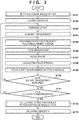
- Fig. 3 is a flowchart of the focus correction formula calculation processing which is executed by the control device 13. Although this processing is executed before the exposure process, this processing need not be performed immediately before the exposure process, and the control device 13 need only store the information related to the calculated correction formula in the storage device 18.
- step S101 the control device 13 determines a plurality of angles of view each of which is a condition for calculating the correction formula.
- Fig. 4 is a flowchart of the processing performed to determine a plurality of candidate angles of view.
- the control device 13 determines, in step S201, the minimum value and the maximum value among the angles of view to be set as candidates, and determines, in step S202, the pitch of angles of view between the determined minimum angle of view and the maximum angle of view. These values may be determined by the user.
- the control device 13 determines, in step S203, a shot layout based on each of the plurality of angles of view obtained in accordance with the minimum value, the maximum value, and the pitch of the angle of view determined in steps S201 and S202.
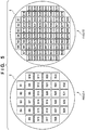
- Fig. 5 shows an example of a shot layout by an angle A of view and an example of a shot layout by an angle B of view smaller than the angle A of view.
- An example of layouts for correction formula calculation calculated in Fig. 4 is shown. Since the angle B of view is smaller than the angle A of view, the number of shot regions formed by the angle B of view is more than the number of shot regions formed by the angle A of view.
- step S102 the substrate 2 is conveyed into the apparatus and mounted on the substrate stage 3.
- step S103 the control device 13 changes the exposure layout in step S103 in accordance with the angle of view determined in step S101.
- the control device 13 performs alignment measurement in step S104, drives the substrate stage 3 (drives the substrate stage in a horizontal direction with respect to the image plane) so that the target shot region will come to the focus measurement position in step S105, and performs the focus measurement in step S106.
- step S107 the control device 13 executes a focus driving operation (drives the substrate stage in a vertical direction with respect to the image plane) in accordance with the focus target value and the focus measurement value measured in step S106.
- step S108 the control device 13 calculates, as a focus residual, the difference of the focus measurement value from the focus target value.
- the control device 13 associates the identification number of the target shot region with the focus residual calculated in step S108 and stores the associated identification number and the focus residual in the storage device 18. The position of the shot region on the substrate can be specified based on the identification number of the shot region.
- step S110 the control device 13 determines whether the measurement has been completed for all of the shot regions. If the measurement has not been completed, the processes of steps S105 to S109 are repeated for the next shot region. If the measurement has been completed for all of the shot regions, the control device 13 determines, in step Sill, whether the measurement has been completed for all of the layouts determined in step S101. If the measurement has not been completed, the process will return to step S103 to repeat the processes for the measurement of the next layout. If the measurement has been completed for all of the layouts, the control device 13 calculates the correction formula in step S112.
- Fig. 6 is a flowchart illustrating correction formula calculation processing performed in step S112.
- the control device 13 obtains the plurality of angles of view determined in step S101.
- the control device 13 determines the angle of view to be set as the processing target from the obtained plurality of angles of view. Processing related to the angle of view determined in step S302 will be performed in the following processes of steps S303 to S306.
- the control device 13 obtains the information of the focus residual for each shot region stored in the storage device 18.
- step S304 the control device 13 classifies the obtained information of the focus residual for each shot region in accordance with the step direction (the plus direction/the minus direction) of the substrate stage 3.
- step S305 the control device 13 performs a polynomial approximation of the relationship between the shot region and the focus residual for each step direction, and stores the obtained result in the storage device 18 (S306).
- step S307 the control device 13 determines whether the processing has been performed for all of the angles of view. If the processing has not been completed for all of the angles of view, the process returns to step S303, and the processing is repeated for the next angle of view. The correction formula is calculated for each angle of view in this manner.
- the correction formula calculation processing includes the following measurement processes.
- the above-described processes (a) to (c) are repeated for each shot region for each of the plurality of angles of view.
- a plurality of correction formulas are calculated (step S112) based on the residual for each shot region obtained for each of the plurality of angles of view based on the measurement process described above.
- step S401 the control device 13 calculates the correction formula corresponding to the exposure layout.
- Fig. 8 shows a flowchart of the correction formula calculation processing performed in step S401.
- step S501 the control device 13 obtains the information of the angle of view (that is, the layout) at the time of exposure from the target exposure recipe.
- step S502 the control device 13 determines whether the obtained layout can be corrected. For example, this is determined by whether the main driving direction of the substrate stage is the same under the layout and exposure conditions set when the correction formula was obtained. If it is determined that obtained layout cannot be corrected, 0 is set as the coefficient of the correction formula.
- the control device 13 confirms, in step S503, whether the angle of view at the time of exposure obtained in step S501 falls outside the range between the maximum value and the minimum value of the plurality of angles of view determined in step S101. If the angle of view obtained in step S501 falls outside the range, the correction formula of an angle of view closest to the exposure angle of view will be obtained in step S504 from the plurality of angles of view determined in step S101. That is, in a case in which the angle of view at the time of exposure is smaller than the minimum angle of view of the plurality of the angles of view, the correction formula for the minimum angle of view will be determined as the correction formula for the angle of view at the time of exposure. Also, in a case in which the angle of view at the time of exposure is larger than the maximum angle of view of the plurality of the angles of view, the correction formula for the maximum angle of view will be determined as the correction formula for the angle of view at the time of exposure.
- step S501 if the angle of view obtained in step S501 falls within the range, the correction formulas used for the two angles of view preceding and succeeding the exposure angle of view will be obtained in step S505.
- the control device 13 performs interpolation of parameters of the correction formulas used for the two angles of view obtained in step S505.
- step S507 the control device 13 determines the correction formula corresponding to the angle of view at the time of exposure using the interpolated parameters.
- the correction formula will be have a degree of one for the sake of descriptive convenience, and linear approximation will be performed by using the two angles of view preceding and succeeding the obtained exposure angle of view to calculate the correction formula.
- X is a position of the shot region in the X direction of the substrate and that Z is the Z direction correction value.
- the coefficients of the two correction formulas are linearly interpolated and the intercepts are linearly interpolated.
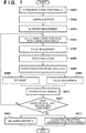
- the substrate is loaded in step S402, and alignment measurement is performed in step S403.
- the control device 13 calculates, in step S404, the Z-direction correction value of each shot region from the correction formula corresponding to the exposure angle of view calculated in step S401.
- the control device 13 performs focus measurement.
- the control device 13 reflects, as an offset, the correction value obtained in step S404 on the instruction value of the substrate stage, and the control device 13 executes focus driving in step S407.
- the control device 13 performs the exposure process in step S408.
- the control device 13 performs, in step S409, the focus measurement during the exposure process and stores (learns), in step S410, the focus residual.
- step S411 the control device 13 determines whether all of the exposure-target shot regions have been exposed. If the exposure process has not been completed for all of the shot regions, the process returns to step S404, and the processing is repeated for the next shot region which has not been exposed yet.
- the correction formula of the newly used exposure angle of view is calculated in step S413 simultaneously with the unloading of the substrate in step S412.
- the newly calculated correction formula is stored in the same manner as the correction formula obtained and stored in Fig. 6 . As a result, the interpolation correction formula calculation accuracy is improved.
- Fig. 9 shows an example of the correction formula result for each angle of view calculated in step S112 that is displayed by the user interface 19.
- An item 91 shows the angle of view.
- Items 92 and 93 each show the step direction of the substrate stage.
- An item 94 shows the calculated correction coefficient.
- Each coefficient of the correction formula obtained by function approximation is expressed as a "Coefficient”, and each intercept is expressed an "Intercept".
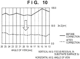
- Fig. 10 is a chart showing the correction result according to the embodiment.
- the abscissa indicates the angle of view of which the focus residual has been obtained, and the ordinate indicates a focus residual 3 ⁇ within the substrate surface.
- focus residual correction can be performed for all of the exposure angles of view according to this embodiment, it is possible to improve the focus accuracy for each angle of view.
- a method of manufacturing an article according to an embodiment of the present invention is suitable for manufacturing an article, for example, a microdevice such as a semiconductor device or an element having a microstructure.
- the method of manufacturing an article according to this embodiment includes a step of forming, using the above-described exposure apparatus, a latent image pattern on a photoresist applied to a substrate (a step of exposing a substrate), and a step of developing the substrate with the latent image pattern formed in the above step.
- the manufacturing method also includes other known steps (for example, oxidation, deposition, vapor deposition, doping, planarization, etching, resist removal, dicing, bonding, and packaging).
- the method of manufacturing an article according to this embodiment is advantageous in at least one of the performance, quality, productivity, and production cost of the article compared to conventional methods.
- Embodiment(s) of the present invention can also be realized by a computer of a system or apparatus that reads out and executes computer executable instructions (e.g., one or more programs) recorded on a storage medium (which may also be referred to more fully as a 'non-transitory computer-readable storage medium') to perform the functions of one or more of the above-described embodiment(s) and/or that includes one or more circuits (e.g., application specific integrated circuit (ASIC)) for performing the functions of one or more of the above-described embodiment(s), and by a method performed by the computer of the system or apparatus by, for example, reading out and executing the computer executable instructions from the storage medium to perform the functions of one or more of the above-described embodiment(s) and/or controlling the one or more circuits to perform the functions of one or more of the above-described embodiment(s).
- computer executable instructions e.g., one or more programs
- a storage medium which may also be referred to more fully as
- the computer may comprise one or more processors (e.g., central processing unit (CPU), micro processing unit (MPU)) and may include a network of separate computers or separate processors to read out and execute the computer executable instructions.
- the computer executable instructions may be provided to the computer, for example, from a network or the storage medium.
- the storage medium may include, for example, one or more of a hard disk, a random-access memory (RAM), a read only memory (ROM), a storage of distributed computing systems, an optical disk (such as a compact disc (CD), digital versatile disc (DVD), or Blu-ray Disc (BD)TM), a flash memory device, a memory card, and the like.
Landscapes
- Physics & Mathematics (AREA)
- General Physics & Mathematics (AREA)
- Exposure And Positioning Against Photoresist Photosensitive Materials (AREA)
- Exposure Of Semiconductors, Excluding Electron Or Ion Beam Exposure (AREA)
- Container, Conveyance, Adherence, Positioning, Of Wafer (AREA)
Abstract
Description
- The present invention relates to an exposure apparatus, a method thereof, and a method of manufacturing an article.
- As an apparatus used in a manufacturing process (lithography process) of a semiconductor device or the like, there is an exposure apparatus that transfers a mask pattern to a substrate. In such an exposure apparatus, the surface of the substrate needs to be arranged accurately on an imaging plane (focus plane) of a projection optical system so a mask pattern will overlap a shot region on the substrate with high accuracy.
- Japanese Patent Laid-Open No.
2015-130407 2004-111995 2000-208391 - Generally, in an exposure apparatus, a focusing operation of arranging a substrate surface on a focus plane is performed by feedback control to increase the accuracy. On the other hand, increasing the speed of the focusing operation is an important requirement for improving throughput. To improve the throughput, it is possible to consider using methods such as increasing the acceleration of the movement of a substrate stage, performing focus measurement in advance by relaxing the settling tolerance of the substrate stage, or the like. However, in such a case, measurement errors can increase since the focus measurement will be performed in a state in which a deviation of the substrate stage is left with respect to a target position. Hence, a more effective correction is required.
- The present invention provides, for example, an exposure apparatus advantageous in improving focus accuracy.
- The present invention in its first aspect provides an exposure apparatus as specified in
claims 1 to 6. - The present invention in its second aspect provides an exposure method as specified in
claims 7 to 10. - The present invention in its third aspect provides a method of manufacturing an article as specified in
claim 11. - Further features of the present invention will become apparent from the following description of exemplary embodiments (with reference to the attached drawings).
-
-
Fig. 1 is a view showing the arrangement of an exposure apparatus according to an embodiment; -
Fig. 2 is a view showing an example of measurement points arranged on a target exposure region; -
Fig. 3 is a flowchart of focus correction formula calculation processing according to the embodiment; -
Fig. 4 is a flowchart of processing for determining an exposure angle of view; -
Fig. 5 is a view showing an example of shot layouts obtained from different angles of view; -
Fig. 6 is a flowchart illustrating correction formula calculation processing; -
Fig. 7 is a flowchart illustrating an exposure process; -
Fig. 8 is a flowchart illustrating the correction formula calculation processing in the exposure process; -
Fig. 9 is a view showing a display example of a correction formula result for each angle of view; and -
Fig. 10 is a graph for explaining an effect of the embodiment. - Various exemplary embodiments, features, and aspects of the invention will be described in detail below with reference to the drawings.
- Embodiments of the present invention will be described in detail below with reference to the accompanying drawings. Note that the following embodiments are merely specific examples of the embodiments of the present invention, and do not limit the present invention. In addition, not all combinations of characteristic features described in the following embodiments are essential to the solution of the problem in the present invention.
-
Fig. 1 is a view showing the arrangement of a reduction projection exposure apparatus which employs a step-and-repeat method according to the embodiment. A projectionoptical system 1 reduces and projects a circuit pattern of a reticle (not shown) and forms a circuit pattern image on a focal plane. In addition, an optical axis AX of the projectionoptical system 1 in a parallel relationship with a Z-axis direction inFig. 1 . A plurality of exposure target regions (shot regions) on which a photoresist has been applied and the same pattern has been formed by a preceding exposure process are arranged on asubstrate 2. Asubstrate stage 3 that holds thesubstrate 2 includes an X stage that moves in an X-axis direction perpendicular to a Z-axis, a Y stage that moves in a Y-axis direction perpendicular to the Z-axis and an X-axis, and a Z stage that moves in a Z-axis direction and rotates about a shaft parallel to the X-, Y-, and Z-axes directions. Hence, by driving thesubstrate stage 3, the surface position of thesubstrate 2 can be adjusted in the direction of the optical axis AX of the projectionoptical system 1 and in a direction along a plane perpendicular to the optical axis AX, and a tilt with respect to a focal plane, that is, a circuit pattern image can also be adjusted. -
Reference numerals 4 to 11 denote elements of a detection optical system provided to detect the position and the tilt of thesubstrate 2.Reference numeral 4 denotes an illumination light source with high luminance such a light-emitting diode, a semiconductor laser, or the like, andreference numeral 5 denotes an illumination lens. Light emitted from theillumination light source 4 is converted into a parallel light beam by theillumination lens 5, is converted into a plurality of light beams via amask 6, enters abending mirror 8 via animaging lens 7, and enters the surface of thesubstrate 2 after its direction is changed by thebending mirror 8. That is, theimaging lens 7 and thebending mirror 8 form a plurality of pinhole images of themask 6 on thesubstrate 2. As shown inFig. 2 , the light beams that have passed through this plurality of pinholes irradiate fivemeasurement points target exposure region 100 of thesubstrate 2, and the light beams are reflected at the respective points. In the example shown inFig. 2 , themeasurement point 71 is at the center oftarget exposure region 100 which intersects with the optical axis AX, and theother measurement points measurement point 71 as the center. The direction of each of the light beams reflected by the fivemeasurement points target exposure region 100 is changed by abending mirror 9, and the light beams subsequently enter a positionsensitive detector 11, on which elements are two-dimensionally arranged, via thedetection lens 10. In this manner, theimaging lens 7, thebending mirror 8, thesubstrate 2, thebending mirror 9, and thedetection lens 10 form pinhole images of themask 6 on the positionsensitive detector 11. Therefore, themask 6, thesubstrate 2, and the positionsensitive detector 11 are at positions which are optically conjugate to each other. - Although the position
sensitive detector 11 is shown schematically inFig. 1 , a plurality of the positionsensitive detector 11 may be arranged in correspondence with the pinholes in a case in which it is difficult to implement an optical arrangement such as that shown inFig. 1 . For example, the positionsensitive detector 11 is formed from a two-dimensional CCD or the like, and is capable of separately detecting the positions of the plurality of light beams incident, via the plurality of pinholes, on the light receiving surface of the positionsensitive detector 11. The positional changes of thesubstrate 2 in the optical axis AX with respect to the projectionoptical system 1 can be detected as shifts in the incident positions of the plurality of light beams on the positionsensitive detector 11. The pieces of optical axis AX direction positional information of the surface of thesubstrate 2 obtained from the fivemeasurement points 71 to 75 in thetarget exposure region 100 of thesubstrate 2 are input as output signals from the positionsensitive detector 11 to acontrol device 13 via a surfaceposition detection device 14. - The displacement of the
substrate stage 3 in the X-axis direction and the Y-axis direction can be measured by a known method by using areference mirror 15 and alaser interferometer 17 arranged on thesubstrate stage 3. A signal indicating the displacement amount of thesubstrate stage 3 is input from thelaser interferometer 17 to thecontrol device 13 via a signal line. Astage driving device 12 controls the movement of thesubstrate stage 3. Thestage driving device 12 receives an instruction signal from thecontrol device 13 via a signal line and drives thesubstrate stage 3 by servo drive in response to this signal. Thestage driving device 12 includes a first driving unit and a second driving unit. The first driving unit adjusts positions x and y and a rotation 0 in a surface perpendicular to the optical axis AX of thesubstrate 2, and the second driving unit adjusts a position z, a tilt α, and a tilt β related to the optical axis AX direction (Z direction) of thesubstrate 2. The surfaceposition detection device 14 detects the surface position of thesubstrate 2 based on each output signal (surface position data) from the positionsensitive detector 11 and transfers the detection result to thecontrol device 13. Based on the detection result obtained by the surfaceposition detection device 14, thecontrol device 13 transmits a predetermined instruction signal to cause the second driving unit of thestage driving device 12 to operate and adjusts the position and the tilt related to the optical axis AX direction of thesubstrate 2. Astorage device 18 can store the data required to drive the stage. Note that thestorage device 18 may be a memory formed in thecontrol device 13. Auser interface 19 can include a console unit for a user to make an operation related to parameter settings, a display unit to display parameters related to stage driving, and the like. - As described above, the
control device 13 performs feedback control, via thestage driving device 12, by arranging the substrate surface on a focus plane when thesubstrate stage 3 is driven in the Z direction. In this case, to improve the throughput, operations such as increasing the acceleration of the movement of thesubstrate stage 3, performing the focus measurement in advance by relaxing the settling tolerance of thesubstrate stage 3, and the like can be considered. However, in such a case, measurement errors can increase because focus measurement will be performed in a state in which a deviation of thesubstrate stage 3 is left with respect to the target position. Hence, thecontrol device 13 needs to correct an instruction value and output the corrected instruction value to thestage driving device 12. The deviation of the measurement value of the substrate stage which is left with respect to the target value in the above-described manner is referred to as a "focus residual" here. According to the examinations by the inventors, it has become evident that this focus residual changes depending on the exposure angle of view (step size). It has also become evident that the focus residual changes depending on the step direction and the position of an exposure target shot region on the substrate. Hence, in this embodiment, thecontrol device 13 will obtain a correction formula corresponding to the angle of view, the step direction, and the position of the target shot region on the substrate. Therefore, thecontrol device 13 will perform processing to calculate a focus correction formula. -
Fig. 3 is a flowchart of the focus correction formula calculation processing which is executed by thecontrol device 13. Although this processing is executed before the exposure process, this processing need not be performed immediately before the exposure process, and thecontrol device 13 need only store the information related to the calculated correction formula in thestorage device 18. - In step S101, the
control device 13 determines a plurality of angles of view each of which is a condition for calculating the correction formula.Fig. 4 is a flowchart of the processing performed to determine a plurality of candidate angles of view. Thecontrol device 13 determines, in step S201, the minimum value and the maximum value among the angles of view to be set as candidates, and determines, in step S202, the pitch of angles of view between the determined minimum angle of view and the maximum angle of view. These values may be determined by the user. Thecontrol device 13 determines, in step S203, a shot layout based on each of the plurality of angles of view obtained in accordance with the minimum value, the maximum value, and the pitch of the angle of view determined in steps S201 and S202. The determined plurality of angles of view and/or shot layouts are stored in thestorage device 18.Fig. 5 shows an example of a shot layout by an angle A of view and an example of a shot layout by an angle B of view smaller than the angle A of view. An example of layouts for correction formula calculation calculated inFig. 4 is shown. Since the angle B of view is smaller than the angle A of view, the number of shot regions formed by the angle B of view is more than the number of shot regions formed by the angle A of view. - The description will be made by referring back to
Fig. 3 . In step S102, thesubstrate 2 is conveyed into the apparatus and mounted on thesubstrate stage 3. In step S103, thecontrol device 13 changes the exposure layout in step S103 in accordance with the angle of view determined in step S101. Thecontrol device 13 performs alignment measurement in step S104, drives the substrate stage 3 (drives the substrate stage in a horizontal direction with respect to the image plane) so that the target shot region will come to the focus measurement position in step S105, and performs the focus measurement in step S106. In step S107, thecontrol device 13 executes a focus driving operation (drives the substrate stage in a vertical direction with respect to the image plane) in accordance with the focus target value and the focus measurement value measured in step S106. In step S108, thecontrol device 13 calculates, as a focus residual, the difference of the focus measurement value from the focus target value. In step S109, thecontrol device 13 associates the identification number of the target shot region with the focus residual calculated in step S108 and stores the associated identification number and the focus residual in thestorage device 18. The position of the shot region on the substrate can be specified based on the identification number of the shot region. In step S110, thecontrol device 13 determines whether the measurement has been completed for all of the shot regions. If the measurement has not been completed, the processes of steps S105 to S109 are repeated for the next shot region. If the measurement has been completed for all of the shot regions, thecontrol device 13 determines, in step Sill, whether the measurement has been completed for all of the layouts determined in step S101. If the measurement has not been completed, the process will return to step S103 to repeat the processes for the measurement of the next layout. If the measurement has been completed for all of the layouts, thecontrol device 13 calculates the correction formula in step S112. -
Fig. 6 is a flowchart illustrating correction formula calculation processing performed in step S112. In step S301, thecontrol device 13 obtains the plurality of angles of view determined in step S101. In step S302, thecontrol device 13 determines the angle of view to be set as the processing target from the obtained plurality of angles of view. Processing related to the angle of view determined in step S302 will be performed in the following processes of steps S303 to S306. In step S303, thecontrol device 13 obtains the information of the focus residual for each shot region stored in thestorage device 18. Next, in step S304, thecontrol device 13 classifies the obtained information of the focus residual for each shot region in accordance with the step direction (the plus direction/the minus direction) of thesubstrate stage 3. In step S305, thecontrol device 13 performs a polynomial approximation of the relationship between the shot region and the focus residual for each step direction, and stores the obtained result in the storage device 18 (S306). In step S307, thecontrol device 13 determines whether the processing has been performed for all of the angles of view. If the processing has not been completed for all of the angles of view, the process returns to step S303, and the processing is repeated for the next angle of view. The correction formula is calculated for each angle of view in this manner. - Referring back to
Fig. 3 , in step S113, the substrate is unloaded, and the processing ends. To summarize the key points of the correction formula calculation processing performed before the exposure process, the correction formula calculation processing includes the following measurement processes. (a) A process of performing focus measurement to obtain a measurement value for the focus driving operation of the substrate stage (step S106). (b) A process of performing a focus driving operation in accordance with the obtained measurement value (step S107). (c) A process of performing focus measurement after the completion of the focus driving operation and calculating a residual of the measurement value obtained by the focus measurement with respect to the target value. In the measurement process, the above-described processes (a) to (c) are repeated for each shot region for each of the plurality of angles of view. In addition, in the correction formula calculation processing, a plurality of correction formulas are calculated (step S112) based on the residual for each shot region obtained for each of the plurality of angles of view based on the measurement process described above. - The exposure process according to the embodiment will be described next with reference to the flowchart of
Fig. 7 . First, in step S401, thecontrol device 13 calculates the correction formula corresponding to the exposure layout.Fig. 8 shows a flowchart of the correction formula calculation processing performed in step S401. In step S501, thecontrol device 13 obtains the information of the angle of view (that is, the layout) at the time of exposure from the target exposure recipe. In step S502, thecontrol device 13 determines whether the obtained layout can be corrected. For example, this is determined by whether the main driving direction of the substrate stage is the same under the layout and exposure conditions set when the correction formula was obtained. If it is determined that obtained layout cannot be corrected, 0 is set as the coefficient of the correction formula. If it is determined that the obtained layout can be corrected, thecontrol device 13 confirms, in step S503, whether the angle of view at the time of exposure obtained in step S501 falls outside the range between the maximum value and the minimum value of the plurality of angles of view determined in step S101. If the angle of view obtained in step S501 falls outside the range, the correction formula of an angle of view closest to the exposure angle of view will be obtained in step S504 from the plurality of angles of view determined in step S101. That is, in a case in which the angle of view at the time of exposure is smaller than the minimum angle of view of the plurality of the angles of view, the correction formula for the minimum angle of view will be determined as the correction formula for the angle of view at the time of exposure. Also, in a case in which the angle of view at the time of exposure is larger than the maximum angle of view of the plurality of the angles of view, the correction formula for the maximum angle of view will be determined as the correction formula for the angle of view at the time of exposure. - On the other hand, if the angle of view obtained in step S501 falls within the range, the correction formulas used for the two angles of view preceding and succeeding the exposure angle of view will be obtained in step S505. For example, if the plurality of angles of view determined in step S101 have been obtained at a pitch of 1.0 mm and the exposure angle of view obtained in step S501 corresponds to 22.5 mm, the correction formulas used for the two angles of view corresponding to 23. 0 mm and 22.0 mm preceding and succeeding the exposure angle of view corresponding to 22.5 mm will be obtained. In step S506, the
control device 13 performs interpolation of parameters of the correction formulas used for the two angles of view obtained in step S505. In step S507, thecontrol device 13 determines the correction formula corresponding to the angle of view at the time of exposure using the interpolated parameters. - In the following example, the correction formula will be have a degree of one for the sake of descriptive convenience, and linear approximation will be performed by using the two angles of view preceding and succeeding the obtained exposure angle of view to calculate the correction formula. When the correction formula of the exposure angle of view corresponding to 22.5 mm is to be obtained, the interpolation correction formula is calculated from the correction formulas of the angle of view corresponding to 23.0 mm (Z = 5.0X + 10.0) and the angle of view corresponding to 22.0 mm (Z = 10.0X + 20.0). However, assume that X is a position of the shot region in the X direction of the substrate and that Z is the Z direction correction value. The coefficients of the two correction formulas are linearly interpolated and the intercepts are linearly interpolated. As a result, the correction formula of the exposure angle of view corresponding to 22.5 mm is Z = 7.5X + 15.
- Referring back to
Fig. 7 , the substrate is loaded in step S402, and alignment measurement is performed in step S403. Thecontrol device 13 calculates, in step S404, the Z-direction correction value of each shot region from the correction formula corresponding to the exposure angle of view calculated in step S401. In step S405, thecontrol device 13 performs focus measurement. In step S406, thecontrol device 13 reflects, as an offset, the correction value obtained in step S404 on the instruction value of the substrate stage, and thecontrol device 13 executes focus driving in step S407. After the completion of the focus driving, thecontrol device 13 performs the exposure process in step S408. Thecontrol device 13 performs, in step S409, the focus measurement during the exposure process and stores (learns), in step S410, the focus residual. - In step S411, the
control device 13 determines whether all of the exposure-target shot regions have been exposed. If the exposure process has not been completed for all of the shot regions, the process returns to step S404, and the processing is repeated for the next shot region which has not been exposed yet. When the exposure process has been completed for all of the shot regions, the correction formula of the newly used exposure angle of view is calculated in step S413 simultaneously with the unloading of the substrate in step S412. The newly calculated correction formula is stored in the same manner as the correction formula obtained and stored inFig. 6 . As a result, the interpolation correction formula calculation accuracy is improved. -
Fig. 9 shows an example of the correction formula result for each angle of view calculated in step S112 that is displayed by theuser interface 19. Anitem 91 shows the angle of view.Items item 94 shows the calculated correction coefficient. Each coefficient of the correction formula obtained by function approximation is expressed as a "Coefficient", and each intercept is expressed an "Intercept". -
Fig. 10 is a chart showing the correction result according to the embodiment. InFig. 10 , the abscissa indicates the angle of view of which the focus residual has been obtained, and the ordinate indicates a focus residual 3σ within the substrate surface. As shown inFig. 10 , since focus residual correction can be performed for all of the exposure angles of view according to this embodiment, it is possible to improve the focus accuracy for each angle of view. - A method of manufacturing an article according to an embodiment of the present invention is suitable for manufacturing an article, for example, a microdevice such as a semiconductor device or an element having a microstructure. The method of manufacturing an article according to this embodiment includes a step of forming, using the above-described exposure apparatus, a latent image pattern on a photoresist applied to a substrate (a step of exposing a substrate), and a step of developing the substrate with the latent image pattern formed in the above step. The manufacturing method also includes other known steps (for example, oxidation, deposition, vapor deposition, doping, planarization, etching, resist removal, dicing, bonding, and packaging). The method of manufacturing an article according to this embodiment is advantageous in at least one of the performance, quality, productivity, and production cost of the article compared to conventional methods.
- Embodiment(s) of the present invention can also be realized by a computer of a system or apparatus that reads out and executes computer executable instructions (e.g., one or more programs) recorded on a storage medium (which may also be referred to more fully as a 'non-transitory computer-readable storage medium') to perform the functions of one or more of the above-described embodiment(s) and/or that includes one or more circuits (e.g., application specific integrated circuit (ASIC)) for performing the functions of one or more of the above-described embodiment(s), and by a method performed by the computer of the system or apparatus by, for example, reading out and executing the computer executable instructions from the storage medium to perform the functions of one or more of the above-described embodiment(s) and/or controlling the one or more circuits to perform the functions of one or more of the above-described embodiment(s). The computer may comprise one or more processors (e.g., central processing unit (CPU), micro processing unit (MPU)) and may include a network of separate computers or separate processors to read out and execute the computer executable instructions. The computer executable instructions may be provided to the computer, for example, from a network or the storage medium. The storage medium may include, for example, one or more of a hard disk, a random-access memory (RAM), a read only memory (ROM), a storage of distributed computing systems, an optical disk (such as a compact disc (CD), digital versatile disc (DVD), or Blu-ray Disc (BD)™), a flash memory device, a memory card, and the like.
- While the present invention has been described with reference to exemplary embodiments, it is to be understood that the invention is not limited to the disclosed exemplary embodiments. The scope of the following claims is to be accorded the broadest interpretation so as to encompass all such modifications and equivalent structures and functions.
Claims (11)
- An exposure apparatus that exposes a substrate (2), comprising:a stage (3) configured to hold and move the substrate; anda controller (13) configured to control focus driving of the stage based on a measurement value and a correction value obtained for the focus driving of the stage for a shot region on the substrate,wherein the controller is configured to determine the correction value in accordance with an angle of view at a time of exposure.
- The apparatus according to claim 1, wherein the controller is configured to determine a correction formula of the angle of view at the time of exposure based on a plurality of correction formulas corresponding to the plurality of angles of view and determines the correction value by using the determined correction formula.
- The apparatus according to claim 2, wherein the correction formula is a formula expressing a correction value corresponding to a position of the shot region on the substrate.
- The apparatus according to claim 2, wherein the plurality of correction formulas are correction formulas corresponding to step directions of the stage other than the plurality of angles of view.
- The apparatus according to claim 2, wherein the controller is configured to determine the correction formula of the angle of view at the time of exposure by interpolating parameters of correction formulas of two angles of view preceding and succeeding the angle of view at the time of exposure among the plurality of angles of view.
- The apparatus according to claim 5, wherein in a case in which the angle of view at the time of exposure is smaller than the minimum angle of view of the plurality of angles of view, the controller determines the correction formula of the minimum angle of view as the correction formula of the angle of view at the time of exposure, and
in a case in which the angle of view at the time of exposure is larger than the maximum angle of view of the plurality of angles of view, the controller determines the correction formula of the maximum angle of view as the correction formula of the angle of view at the time of exposure. - An exposure method of exposing a substrate by using a stage configured to hold and move the substrate, the method comprising:performing focus measurement of obtaining a measurement value for focus driving of the stage for a shot region on the substrate;performing focus driving after reflecting, as an offset, a correction value of the measurement value obtained by the focus measurement on an instruction value of the stage; andexposing the shot region after the completion of the focus driving,wherein the correction value is determined in accordance with angle of view at the time of exposure.
- The method according to claim 7, further comprising determining, in advance, a correction formula of the angle of view at the time of exposure based on a plurality of correction formulas corresponding to a plurality of angles of view, and determining the correction value by using the determined correction formula.
- The method according to claim 8, wherein the correction formula is a formula expressing a correction value corresponding to a position of the shot region on the substrate.
- The method according to claim 9, wherein the determining the correction value includes
performing actual measurement which repeatedly performs the following for each shot region for each of the plurality of angles of view:(a) performing focus measurement to obtain a measurement value for the focus driving of the stage,(b) performing focus driving in accordance with the obtained measurement value, and(c) performing focus measurement after the completion of the focus driving and calculating a residual of a target value of the measurement value obtained by the focus measurement, andcalculating the plurality of correction formulas based on the residual of each shot region obtained for each of the plurality of angles of view by the actual measurement. - A method of manufacturing an article, comprising:exposing a substrate by using an exposure apparatus defined in any one of claims 1 to 6; anddeveloping the substrate exposed in the exposing,wherein an article is manufactured from the developed substrate.
Applications Claiming Priority (1)
| Application Number | Priority Date | Filing Date | Title |
|---|---|---|---|
| JP2018035418A JP6688330B2 (en) | 2018-02-28 | 2018-02-28 | Exposure method, exposure apparatus, determination method, and article manufacturing method |
Publications (2)
| Publication Number | Publication Date |
|---|---|
| EP3534212A1 true EP3534212A1 (en) | 2019-09-04 |
| EP3534212B1 EP3534212B1 (en) | 2023-05-10 |
Family
ID=65365870
Family Applications (1)
| Application Number | Title | Priority Date | Filing Date |
|---|---|---|---|
| EP19156220.6A Active EP3534212B1 (en) | 2018-02-28 | 2019-02-08 | Exposure apparatus, method thereof, and method of manufacturing article |
Country Status (7)
| Country | Link |
|---|---|
| US (1) | US10635005B2 (en) |
| EP (1) | EP3534212B1 (en) |
| JP (1) | JP6688330B2 (en) |
| KR (1) | KR102459126B1 (en) |
| CN (1) | CN110209016B (en) |
| SG (1) | SG10201901269PA (en) |
| TW (1) | TWI712072B (en) |
Families Citing this family (2)
| Publication number | Priority date | Publication date | Assignee | Title |
|---|---|---|---|---|
| JP2023042984A (en) * | 2021-09-15 | 2023-03-28 | キヤノン株式会社 | Exposure apparatus, and method for manufacturing article |
| US20230211436A1 (en) * | 2021-12-30 | 2023-07-06 | Semes Co., Ltd. | Apparatus for treating substrate and method for treating a substrate |
Citations (6)
| Publication number | Priority date | Publication date | Assignee | Title |
|---|---|---|---|---|
| JP2000208391A (en) | 1999-01-11 | 2000-07-28 | Canon Inc | Exposure apparatus and method, and device manufacturing method |
| JP2004111995A (en) | 2003-12-17 | 2004-04-08 | Canon Inc | Projection exposure apparatus and method |
| US20050179880A1 (en) * | 2004-02-18 | 2005-08-18 | Asml Netherlands B.V. | Lithographic apparatus and device manufacturing method with feed-forward focus control |
| US20080291414A1 (en) * | 2007-05-16 | 2008-11-27 | Canon Kabushiki Kaisha | Exposure apparatus and device manufacturing method |
| US20110273686A1 (en) * | 2010-05-07 | 2011-11-10 | Canon Kabushiki Kaisha | Exposure apparatus, exposure method, and method of manufacturing device |
| JP2015130407A (en) | 2014-01-07 | 2015-07-16 | キヤノン株式会社 | Lithographic apparatus, lithographic method, and method of manufacturing article |
Family Cites Families (8)
| Publication number | Priority date | Publication date | Assignee | Title |
|---|---|---|---|---|
| JP3428872B2 (en) * | 1997-08-29 | 2003-07-22 | キヤノン株式会社 | Exposure method and apparatus |
| JP4480339B2 (en) * | 2003-04-03 | 2010-06-16 | 新光電気工業株式会社 | Exposure apparatus and exposure method, and drawing apparatus and drawing method |
| EP1804278A4 (en) * | 2004-09-14 | 2011-03-02 | Nikon Corp | Correction method and exposure device |
| JP2006165216A (en) * | 2004-12-07 | 2006-06-22 | Nikon Corp | Evaluation method, scanning exposure method, and scanning exposure apparatus |
| CN105892238B (en) | 2011-08-31 | 2018-04-13 | Asml荷兰有限公司 | Determine the modified method of focal position, photoetching treatment member and device making method |
| US8755045B2 (en) * | 2012-01-06 | 2014-06-17 | Taiwan Semiconductor Manufacturing Company, Ltd. | Detecting method for forming semiconductor device |
| JP6071628B2 (en) * | 2013-02-22 | 2017-02-01 | キヤノン株式会社 | Exposure apparatus, exposure method, and device manufacturing method |
| JP2017090817A (en) * | 2015-11-16 | 2017-05-25 | キヤノン株式会社 | Exposure apparatus and article manufacturing method |
-
2018
- 2018-02-28 JP JP2018035418A patent/JP6688330B2/en active Active
-
2019
- 2019-02-08 EP EP19156220.6A patent/EP3534212B1/en active Active
- 2019-02-13 US US16/274,569 patent/US10635005B2/en active Active
- 2019-02-14 SG SG10201901269PA patent/SG10201901269PA/en unknown
- 2019-02-20 TW TW108105552A patent/TWI712072B/en active
- 2019-02-22 CN CN201910132118.2A patent/CN110209016B/en active Active
- 2019-02-27 KR KR1020190023009A patent/KR102459126B1/en active Active
Patent Citations (6)
| Publication number | Priority date | Publication date | Assignee | Title |
|---|---|---|---|---|
| JP2000208391A (en) | 1999-01-11 | 2000-07-28 | Canon Inc | Exposure apparatus and method, and device manufacturing method |
| JP2004111995A (en) | 2003-12-17 | 2004-04-08 | Canon Inc | Projection exposure apparatus and method |
| US20050179880A1 (en) * | 2004-02-18 | 2005-08-18 | Asml Netherlands B.V. | Lithographic apparatus and device manufacturing method with feed-forward focus control |
| US20080291414A1 (en) * | 2007-05-16 | 2008-11-27 | Canon Kabushiki Kaisha | Exposure apparatus and device manufacturing method |
| US20110273686A1 (en) * | 2010-05-07 | 2011-11-10 | Canon Kabushiki Kaisha | Exposure apparatus, exposure method, and method of manufacturing device |
| JP2015130407A (en) | 2014-01-07 | 2015-07-16 | キヤノン株式会社 | Lithographic apparatus, lithographic method, and method of manufacturing article |
Also Published As
| Publication number | Publication date |
|---|---|
| KR20190103974A (en) | 2019-09-05 |
| TWI712072B (en) | 2020-12-01 |
| TW201937549A (en) | 2019-09-16 |
| SG10201901269PA (en) | 2019-09-27 |
| KR102459126B1 (en) | 2022-10-26 |
| JP6688330B2 (en) | 2020-04-28 |
| CN110209016A (en) | 2019-09-06 |
| JP2019152685A (en) | 2019-09-12 |
| US10635005B2 (en) | 2020-04-28 |
| CN110209016B (en) | 2021-09-28 |
| EP3534212B1 (en) | 2023-05-10 |
| US20190265599A1 (en) | 2019-08-29 |
Similar Documents
| Publication | Publication Date | Title |
|---|---|---|
| US11835470B2 (en) | Detection apparatus, detection method, exposure apparatus, exposure system, and article manufacturing method | |
| KR102078079B1 (en) | Exposure apparatus, exposure method, and article manufacturing method | |
| EP3379333A2 (en) | Detection apparatus, pattern forming apparatus, obtaining method, detection method, and article manufacturing method | |
| US9910371B2 (en) | Exposure apparatus, exposure method, and device manufacturing method | |
| US10635005B2 (en) | Exposure apparatus, method thereof, and method of manufacturing article | |
| US20170045825A1 (en) | Evaluation method, storage medium, exposure apparatus, exposure method, and method of manufacturing article | |
| KR20180043176A (en) | Lithography apparatus and article manufacturing method | |
| CN111413850B (en) | Exposure apparatus, method for controlling exposure apparatus, and method for manufacturing article | |
| CN119225123A (en) | Exposure device, control method and article manufacturing method | |
| US11194257B2 (en) | Exposure method, exposure apparatus, method of manufacturing article, and measurement method | |
| US9557657B2 (en) | Exposure apparatus and method of manufacturing article | |
| US20240361707A1 (en) | Exposure apparatus, exposure method, and article manufacturing method | |
| JP2020109531A (en) | Exposure device, exposure method and method for producing article | |
| KR102824961B1 (en) | Information processing apparatus, information processing method, program, exposure apparatus, exposure method, and article manufacturing method | |
| KR102938519B1 (en) | Device and method for correcting errors in the two-dimensional accuracy and flatness of a table system | |
| US20260118775A1 (en) | Exposure apparatus, exposure method, and article manufacturing method | |
| KR20180123629A (en) | Optical device, projection optical system, exposure apparatus, and manufacturing method of article | |
| JP2018081238A (en) | Scanning exposure apparatus, control method therefor, and article manufacturing method | |
| TW202314403A (en) | Exposure apparatus and method for manufacturing article capable of accurately adjusting focus with a small size and simple structure while maintaining an improved throughput | |
| JP2023077924A (en) | Exposure apparatus, exposure method, and article manufacturing method | |
| JP2022188520A (en) | Stage device, exposure device, and production method of article | |
| JP2019138957A (en) | Control method of exposure equipment, exposure equipment and article production method | |
| JP2013258211A (en) | Exposure system and method for manufacturing article |
Legal Events
| Date | Code | Title | Description |
|---|---|---|---|
| PUAI | Public reference made under article 153(3) epc to a published international application that has entered the european phase |
Free format text: ORIGINAL CODE: 0009012 |
|
| STAA | Information on the status of an ep patent application or granted ep patent |
Free format text: STATUS: THE APPLICATION HAS BEEN PUBLISHED |
|
| AK | Designated contracting states |
Kind code of ref document: A1 Designated state(s): AL AT BE BG CH CY CZ DE DK EE ES FI FR GB GR HR HU IE IS IT LI LT LU LV MC MK MT NL NO PL PT RO RS SE SI SK SM TR |
|
| AX | Request for extension of the european patent |
Extension state: BA ME |
|
| STAA | Information on the status of an ep patent application or granted ep patent |
Free format text: STATUS: REQUEST FOR EXAMINATION WAS MADE |
|
| 17P | Request for examination filed |
Effective date: 20200304 |
|
| RBV | Designated contracting states (corrected) |
Designated state(s): AL AT BE BG CH CY CZ DE DK EE ES FI FR GB GR HR HU IE IS IT LI LT LU LV MC MK MT NL NO PL PT RO RS SE SI SK SM TR |
|
| STAA | Information on the status of an ep patent application or granted ep patent |
Free format text: STATUS: EXAMINATION IS IN PROGRESS |
|
| 17Q | First examination report despatched |
Effective date: 20210604 |
|
| GRAP | Despatch of communication of intention to grant a patent |
Free format text: ORIGINAL CODE: EPIDOSNIGR1 |
|
| STAA | Information on the status of an ep patent application or granted ep patent |
Free format text: STATUS: GRANT OF PATENT IS INTENDED |
|
| INTG | Intention to grant announced |
Effective date: 20221219 |
|
| GRAS | Grant fee paid |
Free format text: ORIGINAL CODE: EPIDOSNIGR3 |
|
| GRAA | (expected) grant |
Free format text: ORIGINAL CODE: 0009210 |
|
| STAA | Information on the status of an ep patent application or granted ep patent |
Free format text: STATUS: THE PATENT HAS BEEN GRANTED |
|
| AK | Designated contracting states |
Kind code of ref document: B1 Designated state(s): AL AT BE BG CH CY CZ DE DK EE ES FI FR GB GR HR HU IE IS IT LI LT LU LV MC MK MT NL NO PL PT RO RS SE SI SK SM TR |
|
| REG | Reference to a national code |
Ref country code: GB Ref legal event code: FG4D |
|
| REG | Reference to a national code |
Ref country code: AT Ref legal event code: REF Ref document number: 1567286 Country of ref document: AT Kind code of ref document: T Effective date: 20230515 Ref country code: CH Ref legal event code: EP |
|
| REG | Reference to a national code |
Ref country code: DE Ref legal event code: R096 Ref document number: 602019028582 Country of ref document: DE |
|
| REG | Reference to a national code |
Ref country code: IE Ref legal event code: FG4D |
|
| REG | Reference to a national code |
Ref country code: LT Ref legal event code: MG9D |
|
| REG | Reference to a national code |
Ref country code: NL Ref legal event code: MP Effective date: 20230510 |
|
| REG | Reference to a national code |
Ref country code: AT Ref legal event code: MK05 Ref document number: 1567286 Country of ref document: AT Kind code of ref document: T Effective date: 20230510 |
|
| PG25 | Lapsed in a contracting state [announced via postgrant information from national office to epo] |
Ref country code: SE Free format text: LAPSE BECAUSE OF FAILURE TO SUBMIT A TRANSLATION OF THE DESCRIPTION OR TO PAY THE FEE WITHIN THE PRESCRIBED TIME-LIMIT Effective date: 20230510 Ref country code: PT Free format text: LAPSE BECAUSE OF FAILURE TO SUBMIT A TRANSLATION OF THE DESCRIPTION OR TO PAY THE FEE WITHIN THE PRESCRIBED TIME-LIMIT Effective date: 20230911 Ref country code: NO Free format text: LAPSE BECAUSE OF FAILURE TO SUBMIT A TRANSLATION OF THE DESCRIPTION OR TO PAY THE FEE WITHIN THE PRESCRIBED TIME-LIMIT Effective date: 20230810 Ref country code: NL Free format text: LAPSE BECAUSE OF FAILURE TO SUBMIT A TRANSLATION OF THE DESCRIPTION OR TO PAY THE FEE WITHIN THE PRESCRIBED TIME-LIMIT Effective date: 20230510 Ref country code: ES Free format text: LAPSE BECAUSE OF FAILURE TO SUBMIT A TRANSLATION OF THE DESCRIPTION OR TO PAY THE FEE WITHIN THE PRESCRIBED TIME-LIMIT Effective date: 20230510 Ref country code: AT Free format text: LAPSE BECAUSE OF FAILURE TO SUBMIT A TRANSLATION OF THE DESCRIPTION OR TO PAY THE FEE WITHIN THE PRESCRIBED TIME-LIMIT Effective date: 20230510 |
|
| PG25 | Lapsed in a contracting state [announced via postgrant information from national office to epo] |
Ref country code: RS Free format text: LAPSE BECAUSE OF FAILURE TO SUBMIT A TRANSLATION OF THE DESCRIPTION OR TO PAY THE FEE WITHIN THE PRESCRIBED TIME-LIMIT Effective date: 20230510 Ref country code: PL Free format text: LAPSE BECAUSE OF FAILURE TO SUBMIT A TRANSLATION OF THE DESCRIPTION OR TO PAY THE FEE WITHIN THE PRESCRIBED TIME-LIMIT Effective date: 20230510 Ref country code: LV Free format text: LAPSE BECAUSE OF FAILURE TO SUBMIT A TRANSLATION OF THE DESCRIPTION OR TO PAY THE FEE WITHIN THE PRESCRIBED TIME-LIMIT Effective date: 20230510 Ref country code: LT Free format text: LAPSE BECAUSE OF FAILURE TO SUBMIT A TRANSLATION OF THE DESCRIPTION OR TO PAY THE FEE WITHIN THE PRESCRIBED TIME-LIMIT Effective date: 20230510 Ref country code: IS Free format text: LAPSE BECAUSE OF FAILURE TO SUBMIT A TRANSLATION OF THE DESCRIPTION OR TO PAY THE FEE WITHIN THE PRESCRIBED TIME-LIMIT Effective date: 20230910 Ref country code: HR Free format text: LAPSE BECAUSE OF FAILURE TO SUBMIT A TRANSLATION OF THE DESCRIPTION OR TO PAY THE FEE WITHIN THE PRESCRIBED TIME-LIMIT Effective date: 20230510 Ref country code: GR Free format text: LAPSE BECAUSE OF FAILURE TO SUBMIT A TRANSLATION OF THE DESCRIPTION OR TO PAY THE FEE WITHIN THE PRESCRIBED TIME-LIMIT Effective date: 20230811 |
|
| PG25 | Lapsed in a contracting state [announced via postgrant information from national office to epo] |
Ref country code: FI Free format text: LAPSE BECAUSE OF FAILURE TO SUBMIT A TRANSLATION OF THE DESCRIPTION OR TO PAY THE FEE WITHIN THE PRESCRIBED TIME-LIMIT Effective date: 20230510 |
|
| PG25 | Lapsed in a contracting state [announced via postgrant information from national office to epo] |
Ref country code: SK Free format text: LAPSE BECAUSE OF FAILURE TO SUBMIT A TRANSLATION OF THE DESCRIPTION OR TO PAY THE FEE WITHIN THE PRESCRIBED TIME-LIMIT Effective date: 20230510 |
|
| PG25 | Lapsed in a contracting state [announced via postgrant information from national office to epo] |
Ref country code: SM Free format text: LAPSE BECAUSE OF FAILURE TO SUBMIT A TRANSLATION OF THE DESCRIPTION OR TO PAY THE FEE WITHIN THE PRESCRIBED TIME-LIMIT Effective date: 20230510 Ref country code: SK Free format text: LAPSE BECAUSE OF FAILURE TO SUBMIT A TRANSLATION OF THE DESCRIPTION OR TO PAY THE FEE WITHIN THE PRESCRIBED TIME-LIMIT Effective date: 20230510 Ref country code: RO Free format text: LAPSE BECAUSE OF FAILURE TO SUBMIT A TRANSLATION OF THE DESCRIPTION OR TO PAY THE FEE WITHIN THE PRESCRIBED TIME-LIMIT Effective date: 20230510 Ref country code: EE Free format text: LAPSE BECAUSE OF FAILURE TO SUBMIT A TRANSLATION OF THE DESCRIPTION OR TO PAY THE FEE WITHIN THE PRESCRIBED TIME-LIMIT Effective date: 20230510 Ref country code: DK Free format text: LAPSE BECAUSE OF FAILURE TO SUBMIT A TRANSLATION OF THE DESCRIPTION OR TO PAY THE FEE WITHIN THE PRESCRIBED TIME-LIMIT Effective date: 20230510 Ref country code: CZ Free format text: LAPSE BECAUSE OF FAILURE TO SUBMIT A TRANSLATION OF THE DESCRIPTION OR TO PAY THE FEE WITHIN THE PRESCRIBED TIME-LIMIT Effective date: 20230510 |
|
| REG | Reference to a national code |
Ref country code: DE Ref legal event code: R097 Ref document number: 602019028582 Country of ref document: DE |
|
| PLBE | No opposition filed within time limit |
Free format text: ORIGINAL CODE: 0009261 |
|
| STAA | Information on the status of an ep patent application or granted ep patent |
Free format text: STATUS: NO OPPOSITION FILED WITHIN TIME LIMIT |
|
| 26N | No opposition filed |
Effective date: 20240213 |
|
| PG25 | Lapsed in a contracting state [announced via postgrant information from national office to epo] |
Ref country code: SI Free format text: LAPSE BECAUSE OF FAILURE TO SUBMIT A TRANSLATION OF THE DESCRIPTION OR TO PAY THE FEE WITHIN THE PRESCRIBED TIME-LIMIT Effective date: 20230510 |
|
| PG25 | Lapsed in a contracting state [announced via postgrant information from national office to epo] |
Ref country code: SI Free format text: LAPSE BECAUSE OF FAILURE TO SUBMIT A TRANSLATION OF THE DESCRIPTION OR TO PAY THE FEE WITHIN THE PRESCRIBED TIME-LIMIT Effective date: 20230510 |
|
| PG25 | Lapsed in a contracting state [announced via postgrant information from national office to epo] |
Ref country code: MC Free format text: LAPSE BECAUSE OF FAILURE TO SUBMIT A TRANSLATION OF THE DESCRIPTION OR TO PAY THE FEE WITHIN THE PRESCRIBED TIME-LIMIT Effective date: 20230510 |
|
| REG | Reference to a national code |
Ref country code: CH Ref legal event code: PL |
|
| PG25 | Lapsed in a contracting state [announced via postgrant information from national office to epo] |
Ref country code: LU Free format text: LAPSE BECAUSE OF NON-PAYMENT OF DUE FEES Effective date: 20240208 |
|
| PG25 | Lapsed in a contracting state [announced via postgrant information from national office to epo] |
Ref country code: CH Free format text: LAPSE BECAUSE OF NON-PAYMENT OF DUE FEES Effective date: 20240229 |
|
| GBPC | Gb: european patent ceased through non-payment of renewal fee |
Effective date: 20240208 |
|
| PG25 | Lapsed in a contracting state [announced via postgrant information from national office to epo] |
Ref country code: LU Free format text: LAPSE BECAUSE OF NON-PAYMENT OF DUE FEES Effective date: 20240208 Ref country code: CH Free format text: LAPSE BECAUSE OF NON-PAYMENT OF DUE FEES Effective date: 20240229 |
|
| PG25 | Lapsed in a contracting state [announced via postgrant information from national office to epo] |
Ref country code: BG Free format text: LAPSE BECAUSE OF FAILURE TO SUBMIT A TRANSLATION OF THE DESCRIPTION OR TO PAY THE FEE WITHIN THE PRESCRIBED TIME-LIMIT Effective date: 20230510 |
|
| PG25 | Lapsed in a contracting state [announced via postgrant information from national office to epo] |
Ref country code: BG Free format text: LAPSE BECAUSE OF FAILURE TO SUBMIT A TRANSLATION OF THE DESCRIPTION OR TO PAY THE FEE WITHIN THE PRESCRIBED TIME-LIMIT Effective date: 20230510 |
|
| REG | Reference to a national code |
Ref country code: BE Ref legal event code: MM Effective date: 20240229 |
|
| PG25 | Lapsed in a contracting state [announced via postgrant information from national office to epo] |
Ref country code: BE Free format text: LAPSE BECAUSE OF NON-PAYMENT OF DUE FEES Effective date: 20240229 |
|
| PG25 | Lapsed in a contracting state [announced via postgrant information from national office to epo] |
Ref country code: GB Free format text: LAPSE BECAUSE OF NON-PAYMENT OF DUE FEES Effective date: 20240208 |
|
| PG25 | Lapsed in a contracting state [announced via postgrant information from national office to epo] |
Ref country code: IE Free format text: LAPSE BECAUSE OF NON-PAYMENT OF DUE FEES Effective date: 20240208 |
|
| PG25 | Lapsed in a contracting state [announced via postgrant information from national office to epo] |
Ref country code: IE Free format text: LAPSE BECAUSE OF NON-PAYMENT OF DUE FEES Effective date: 20240208 Ref country code: GB Free format text: LAPSE BECAUSE OF NON-PAYMENT OF DUE FEES Effective date: 20240208 Ref country code: BE Free format text: LAPSE BECAUSE OF NON-PAYMENT OF DUE FEES Effective date: 20240229 |
|
| PG25 | Lapsed in a contracting state [announced via postgrant information from national office to epo] |
Ref country code: CY Free format text: LAPSE BECAUSE OF FAILURE TO SUBMIT A TRANSLATION OF THE DESCRIPTION OR TO PAY THE FEE WITHIN THE PRESCRIBED TIME-LIMIT; INVALID AB INITIO Effective date: 20190208 |
|
| PG25 | Lapsed in a contracting state [announced via postgrant information from national office to epo] |
Ref country code: HU Free format text: LAPSE BECAUSE OF FAILURE TO SUBMIT A TRANSLATION OF THE DESCRIPTION OR TO PAY THE FEE WITHIN THE PRESCRIBED TIME-LIMIT; INVALID AB INITIO Effective date: 20190208 |
|
| PG25 | Lapsed in a contracting state [announced via postgrant information from national office to epo] |
Ref country code: TR Free format text: LAPSE BECAUSE OF FAILURE TO SUBMIT A TRANSLATION OF THE DESCRIPTION OR TO PAY THE FEE WITHIN THE PRESCRIBED TIME-LIMIT Effective date: 20230510 |
|
| PGFP | Annual fee paid to national office [announced via postgrant information from national office to epo] |
Ref country code: DE Payment date: 20260121 Year of fee payment: 8 |
|
| PGFP | Annual fee paid to national office [announced via postgrant information from national office to epo] |
Ref country code: IT Payment date: 20260121 Year of fee payment: 8 |
|
| PGFP | Annual fee paid to national office [announced via postgrant information from national office to epo] |
Ref country code: FR Payment date: 20260121 Year of fee payment: 8 |