EP3534193A1 - Optical wavelength conversion member and light-emitting device - Google Patents
Optical wavelength conversion member and light-emitting device Download PDFInfo
- Publication number
- EP3534193A1 EP3534193A1 EP17865959.5A EP17865959A EP3534193A1 EP 3534193 A1 EP3534193 A1 EP 3534193A1 EP 17865959 A EP17865959 A EP 17865959A EP 3534193 A1 EP3534193 A1 EP 3534193A1
- Authority
- EP
- European Patent Office
- Prior art keywords
- wavelength conversion
- phase
- fluorescent
- optical wavelength
- conversion member
- Prior art date
- Legal status (The legal status is an assumption and is not a legal conclusion. Google has not performed a legal analysis and makes no representation as to the accuracy of the status listed.)
- Granted
Links
Images


Classifications
-
- C—CHEMISTRY; METALLURGY
- C04—CEMENTS; CONCRETE; ARTIFICIAL STONE; CERAMICS; REFRACTORIES
- C04B—LIME, MAGNESIA; SLAG; CEMENTS; COMPOSITIONS THEREOF, e.g. MORTARS, CONCRETE OR LIKE BUILDING MATERIALS; ARTIFICIAL STONE; CERAMICS; REFRACTORIES; TREATMENT OF NATURAL STONE
- C04B35/00—Shaped ceramic products characterised by their composition; Ceramics compositions; Processing powders of inorganic compounds preparatory to the manufacturing of ceramic products
- C04B35/01—Shaped ceramic products characterised by their composition; Ceramics compositions; Processing powders of inorganic compounds preparatory to the manufacturing of ceramic products based on oxide ceramics
- C04B35/44—Shaped ceramic products characterised by their composition; Ceramics compositions; Processing powders of inorganic compounds preparatory to the manufacturing of ceramic products based on oxide ceramics based on aluminates
-
- C—CHEMISTRY; METALLURGY
- C09—DYES; PAINTS; POLISHES; NATURAL RESINS; ADHESIVES; COMPOSITIONS NOT OTHERWISE PROVIDED FOR; APPLICATIONS OF MATERIALS NOT OTHERWISE PROVIDED FOR
- C09K—MATERIALS FOR MISCELLANEOUS APPLICATIONS, NOT PROVIDED FOR ELSEWHERE
- C09K11/00—Luminescent materials, e.g. electroluminescent or chemiluminescent
- C09K11/08—Luminescent materials, e.g. electroluminescent or chemiluminescent containing inorganic luminescent materials
- C09K11/77—Luminescent materials, e.g. electroluminescent or chemiluminescent containing inorganic luminescent materials containing rare earth metals
- C09K11/7766—Luminescent materials, e.g. electroluminescent or chemiluminescent containing inorganic luminescent materials containing rare earth metals containing two or more rare earth metals
- C09K11/7774—Aluminates
-
- C—CHEMISTRY; METALLURGY
- C04—CEMENTS; CONCRETE; ARTIFICIAL STONE; CERAMICS; REFRACTORIES
- C04B—LIME, MAGNESIA; SLAG; CEMENTS; COMPOSITIONS THEREOF, e.g. MORTARS, CONCRETE OR LIKE BUILDING MATERIALS; ARTIFICIAL STONE; CERAMICS; REFRACTORIES; TREATMENT OF NATURAL STONE
- C04B35/00—Shaped ceramic products characterised by their composition; Ceramics compositions; Processing powders of inorganic compounds preparatory to the manufacturing of ceramic products
- C04B35/01—Shaped ceramic products characterised by their composition; Ceramics compositions; Processing powders of inorganic compounds preparatory to the manufacturing of ceramic products based on oxide ceramics
-
- C—CHEMISTRY; METALLURGY
- C04—CEMENTS; CONCRETE; ARTIFICIAL STONE; CERAMICS; REFRACTORIES
- C04B—LIME, MAGNESIA; SLAG; CEMENTS; COMPOSITIONS THEREOF, e.g. MORTARS, CONCRETE OR LIKE BUILDING MATERIALS; ARTIFICIAL STONE; CERAMICS; REFRACTORIES; TREATMENT OF NATURAL STONE
- C04B35/00—Shaped ceramic products characterised by their composition; Ceramics compositions; Processing powders of inorganic compounds preparatory to the manufacturing of ceramic products
- C04B35/50—Shaped ceramic products characterised by their composition; Ceramics compositions; Processing powders of inorganic compounds preparatory to the manufacturing of ceramic products based on rare-earth compounds
-
- C—CHEMISTRY; METALLURGY
- C04—CEMENTS; CONCRETE; ARTIFICIAL STONE; CERAMICS; REFRACTORIES
- C04B—LIME, MAGNESIA; SLAG; CEMENTS; COMPOSITIONS THEREOF, e.g. MORTARS, CONCRETE OR LIKE BUILDING MATERIALS; ARTIFICIAL STONE; CERAMICS; REFRACTORIES; TREATMENT OF NATURAL STONE
- C04B35/00—Shaped ceramic products characterised by their composition; Ceramics compositions; Processing powders of inorganic compounds preparatory to the manufacturing of ceramic products
- C04B35/622—Forming processes; Processing powders of inorganic compounds preparatory to the manufacturing of ceramic products
- C04B35/626—Preparing or treating the powders individually or as batches ; preparing or treating macroscopic reinforcing agents for ceramic products, e.g. fibres; mechanical aspects section B
- C04B35/62605—Treating the starting powders individually or as mixtures
- C04B35/6261—Milling
-
- C—CHEMISTRY; METALLURGY
- C04—CEMENTS; CONCRETE; ARTIFICIAL STONE; CERAMICS; REFRACTORIES
- C04B—LIME, MAGNESIA; SLAG; CEMENTS; COMPOSITIONS THEREOF, e.g. MORTARS, CONCRETE OR LIKE BUILDING MATERIALS; ARTIFICIAL STONE; CERAMICS; REFRACTORIES; TREATMENT OF NATURAL STONE
- C04B35/00—Shaped ceramic products characterised by their composition; Ceramics compositions; Processing powders of inorganic compounds preparatory to the manufacturing of ceramic products
- C04B35/622—Forming processes; Processing powders of inorganic compounds preparatory to the manufacturing of ceramic products
- C04B35/64—Burning or sintering processes
-
- C—CHEMISTRY; METALLURGY
- C09—DYES; PAINTS; POLISHES; NATURAL RESINS; ADHESIVES; COMPOSITIONS NOT OTHERWISE PROVIDED FOR; APPLICATIONS OF MATERIALS NOT OTHERWISE PROVIDED FOR
- C09K—MATERIALS FOR MISCELLANEOUS APPLICATIONS, NOT PROVIDED FOR ELSEWHERE
- C09K11/00—Luminescent materials, e.g. electroluminescent or chemiluminescent
- C09K11/08—Luminescent materials, e.g. electroluminescent or chemiluminescent containing inorganic luminescent materials
- C09K11/62—Luminescent materials, e.g. electroluminescent or chemiluminescent containing inorganic luminescent materials containing gallium, indium or thallium
- C09K11/621—Chalcogenides
-
- C—CHEMISTRY; METALLURGY
- C09—DYES; PAINTS; POLISHES; NATURAL RESINS; ADHESIVES; COMPOSITIONS NOT OTHERWISE PROVIDED FOR; APPLICATIONS OF MATERIALS NOT OTHERWISE PROVIDED FOR
- C09K—MATERIALS FOR MISCELLANEOUS APPLICATIONS, NOT PROVIDED FOR ELSEWHERE
- C09K11/00—Luminescent materials, e.g. electroluminescent or chemiluminescent
- C09K11/08—Luminescent materials, e.g. electroluminescent or chemiluminescent containing inorganic luminescent materials
- C09K11/77—Luminescent materials, e.g. electroluminescent or chemiluminescent containing inorganic luminescent materials containing rare earth metals
- C09K11/7715—Luminescent materials, e.g. electroluminescent or chemiluminescent containing inorganic luminescent materials containing rare earth metals containing cerium
- C09K11/7721—Aluminates
-
- G—PHYSICS
- G02—OPTICS
- G02B—OPTICAL ELEMENTS, SYSTEMS OR APPARATUS
- G02B5/00—Optical elements other than lenses
- G02B5/20—Filters
-
- H—ELECTRICITY
- H10—SEMICONDUCTOR DEVICES; ELECTRIC SOLID-STATE DEVICES NOT OTHERWISE PROVIDED FOR
- H10H—INORGANIC LIGHT-EMITTING SEMICONDUCTOR DEVICES HAVING POTENTIAL BARRIERS
- H10H20/00—Individual inorganic light-emitting semiconductor devices having potential barriers, e.g. light-emitting diodes [LED]
- H10H20/01—Manufacture or treatment
- H10H20/036—Manufacture or treatment of packages
- H10H20/0361—Manufacture or treatment of packages of wavelength conversion means
-
- H—ELECTRICITY
- H10—SEMICONDUCTOR DEVICES; ELECTRIC SOLID-STATE DEVICES NOT OTHERWISE PROVIDED FOR
- H10H—INORGANIC LIGHT-EMITTING SEMICONDUCTOR DEVICES HAVING POTENTIAL BARRIERS
- H10H20/00—Individual inorganic light-emitting semiconductor devices having potential barriers, e.g. light-emitting diodes [LED]
- H10H20/80—Constructional details
- H10H20/85—Packages
- H10H20/851—Wavelength conversion means
-
- H—ELECTRICITY
- H10—SEMICONDUCTOR DEVICES; ELECTRIC SOLID-STATE DEVICES NOT OTHERWISE PROVIDED FOR
- H10H—INORGANIC LIGHT-EMITTING SEMICONDUCTOR DEVICES HAVING POTENTIAL BARRIERS
- H10H20/00—Individual inorganic light-emitting semiconductor devices having potential barriers, e.g. light-emitting diodes [LED]
- H10H20/80—Constructional details
- H10H20/85—Packages
- H10H20/851—Wavelength conversion means
- H10H20/8511—Wavelength conversion means characterised by their material, e.g. binder
- H10H20/8512—Wavelength conversion materials
-
- C—CHEMISTRY; METALLURGY
- C04—CEMENTS; CONCRETE; ARTIFICIAL STONE; CERAMICS; REFRACTORIES
- C04B—LIME, MAGNESIA; SLAG; CEMENTS; COMPOSITIONS THEREOF, e.g. MORTARS, CONCRETE OR LIKE BUILDING MATERIALS; ARTIFICIAL STONE; CERAMICS; REFRACTORIES; TREATMENT OF NATURAL STONE
- C04B2235/00—Aspects relating to ceramic starting mixtures or sintered ceramic products
- C04B2235/02—Composition of constituents of the starting material or of secondary phases of the final product
- C04B2235/30—Constituents and secondary phases not being of a fibrous nature
- C04B2235/32—Metal oxides, mixed metal oxides, or oxide-forming salts thereof, e.g. carbonates, nitrates, (oxy)hydroxides, chlorides
- C04B2235/3224—Rare earth oxide or oxide forming salts thereof, e.g. scandium oxide
-
- C—CHEMISTRY; METALLURGY
- C04—CEMENTS; CONCRETE; ARTIFICIAL STONE; CERAMICS; REFRACTORIES
- C04B—LIME, MAGNESIA; SLAG; CEMENTS; COMPOSITIONS THEREOF, e.g. MORTARS, CONCRETE OR LIKE BUILDING MATERIALS; ARTIFICIAL STONE; CERAMICS; REFRACTORIES; TREATMENT OF NATURAL STONE
- C04B2235/00—Aspects relating to ceramic starting mixtures or sintered ceramic products
- C04B2235/02—Composition of constituents of the starting material or of secondary phases of the final product
- C04B2235/30—Constituents and secondary phases not being of a fibrous nature
- C04B2235/32—Metal oxides, mixed metal oxides, or oxide-forming salts thereof, e.g. carbonates, nitrates, (oxy)hydroxides, chlorides
- C04B2235/3224—Rare earth oxide or oxide forming salts thereof, e.g. scandium oxide
- C04B2235/3225—Yttrium oxide or oxide-forming salts thereof
-
- C—CHEMISTRY; METALLURGY
- C04—CEMENTS; CONCRETE; ARTIFICIAL STONE; CERAMICS; REFRACTORIES
- C04B—LIME, MAGNESIA; SLAG; CEMENTS; COMPOSITIONS THEREOF, e.g. MORTARS, CONCRETE OR LIKE BUILDING MATERIALS; ARTIFICIAL STONE; CERAMICS; REFRACTORIES; TREATMENT OF NATURAL STONE
- C04B2235/00—Aspects relating to ceramic starting mixtures or sintered ceramic products
- C04B2235/02—Composition of constituents of the starting material or of secondary phases of the final product
- C04B2235/30—Constituents and secondary phases not being of a fibrous nature
- C04B2235/32—Metal oxides, mixed metal oxides, or oxide-forming salts thereof, e.g. carbonates, nitrates, (oxy)hydroxides, chlorides
- C04B2235/3224—Rare earth oxide or oxide forming salts thereof, e.g. scandium oxide
- C04B2235/3229—Cerium oxides or oxide-forming salts thereof
-
- C—CHEMISTRY; METALLURGY
- C04—CEMENTS; CONCRETE; ARTIFICIAL STONE; CERAMICS; REFRACTORIES
- C04B—LIME, MAGNESIA; SLAG; CEMENTS; COMPOSITIONS THEREOF, e.g. MORTARS, CONCRETE OR LIKE BUILDING MATERIALS; ARTIFICIAL STONE; CERAMICS; REFRACTORIES; TREATMENT OF NATURAL STONE
- C04B2235/00—Aspects relating to ceramic starting mixtures or sintered ceramic products
- C04B2235/02—Composition of constituents of the starting material or of secondary phases of the final product
- C04B2235/30—Constituents and secondary phases not being of a fibrous nature
- C04B2235/32—Metal oxides, mixed metal oxides, or oxide-forming salts thereof, e.g. carbonates, nitrates, (oxy)hydroxides, chlorides
- C04B2235/3286—Gallium oxides, gallates, indium oxides, indates, thallium oxides, thallates or oxide forming salts thereof, e.g. zinc gallate
-
- C—CHEMISTRY; METALLURGY
- C04—CEMENTS; CONCRETE; ARTIFICIAL STONE; CERAMICS; REFRACTORIES
- C04B—LIME, MAGNESIA; SLAG; CEMENTS; COMPOSITIONS THEREOF, e.g. MORTARS, CONCRETE OR LIKE BUILDING MATERIALS; ARTIFICIAL STONE; CERAMICS; REFRACTORIES; TREATMENT OF NATURAL STONE
- C04B2235/00—Aspects relating to ceramic starting mixtures or sintered ceramic products
- C04B2235/02—Composition of constituents of the starting material or of secondary phases of the final product
- C04B2235/50—Constituents or additives of the starting mixture chosen for their shape or used because of their shape or their physical appearance
- C04B2235/54—Particle size related information
- C04B2235/5418—Particle size related information expressed by the size of the particles or aggregates thereof
- C04B2235/5436—Particle size related information expressed by the size of the particles or aggregates thereof micrometer sized, i.e. from 1 to 100 micron
-
- C—CHEMISTRY; METALLURGY
- C04—CEMENTS; CONCRETE; ARTIFICIAL STONE; CERAMICS; REFRACTORIES
- C04B—LIME, MAGNESIA; SLAG; CEMENTS; COMPOSITIONS THEREOF, e.g. MORTARS, CONCRETE OR LIKE BUILDING MATERIALS; ARTIFICIAL STONE; CERAMICS; REFRACTORIES; TREATMENT OF NATURAL STONE
- C04B2235/00—Aspects relating to ceramic starting mixtures or sintered ceramic products
- C04B2235/02—Composition of constituents of the starting material or of secondary phases of the final product
- C04B2235/50—Constituents or additives of the starting mixture chosen for their shape or used because of their shape or their physical appearance
- C04B2235/54—Particle size related information
- C04B2235/5418—Particle size related information expressed by the size of the particles or aggregates thereof
- C04B2235/5445—Particle size related information expressed by the size of the particles or aggregates thereof submicron sized, i.e. from 0,1 to 1 micron
-
- C—CHEMISTRY; METALLURGY
- C04—CEMENTS; CONCRETE; ARTIFICIAL STONE; CERAMICS; REFRACTORIES
- C04B—LIME, MAGNESIA; SLAG; CEMENTS; COMPOSITIONS THEREOF, e.g. MORTARS, CONCRETE OR LIKE BUILDING MATERIALS; ARTIFICIAL STONE; CERAMICS; REFRACTORIES; TREATMENT OF NATURAL STONE
- C04B2235/00—Aspects relating to ceramic starting mixtures or sintered ceramic products
- C04B2235/65—Aspects relating to heat treatments of ceramic bodies such as green ceramics or pre-sintered ceramics, e.g. burning, sintering or melting processes
- C04B2235/656—Aspects relating to heat treatments of ceramic bodies such as green ceramics or pre-sintered ceramics, e.g. burning, sintering or melting processes characterised by specific heating conditions during heat treatment
- C04B2235/6567—Treatment time
-
- C—CHEMISTRY; METALLURGY
- C04—CEMENTS; CONCRETE; ARTIFICIAL STONE; CERAMICS; REFRACTORIES
- C04B—LIME, MAGNESIA; SLAG; CEMENTS; COMPOSITIONS THEREOF, e.g. MORTARS, CONCRETE OR LIKE BUILDING MATERIALS; ARTIFICIAL STONE; CERAMICS; REFRACTORIES; TREATMENT OF NATURAL STONE
- C04B2235/00—Aspects relating to ceramic starting mixtures or sintered ceramic products
- C04B2235/70—Aspects relating to sintered or melt-casted ceramic products
- C04B2235/74—Physical characteristics
- C04B2235/76—Crystal structural characteristics, e.g. symmetry
- C04B2235/762—Cubic symmetry, e.g. beta-SiC
- C04B2235/764—Garnet structure A3B2(CO4)3
-
- C—CHEMISTRY; METALLURGY
- C04—CEMENTS; CONCRETE; ARTIFICIAL STONE; CERAMICS; REFRACTORIES
- C04B—LIME, MAGNESIA; SLAG; CEMENTS; COMPOSITIONS THEREOF, e.g. MORTARS, CONCRETE OR LIKE BUILDING MATERIALS; ARTIFICIAL STONE; CERAMICS; REFRACTORIES; TREATMENT OF NATURAL STONE
- C04B2235/00—Aspects relating to ceramic starting mixtures or sintered ceramic products
- C04B2235/70—Aspects relating to sintered or melt-casted ceramic products
- C04B2235/74—Physical characteristics
- C04B2235/77—Density
-
- C—CHEMISTRY; METALLURGY
- C04—CEMENTS; CONCRETE; ARTIFICIAL STONE; CERAMICS; REFRACTORIES
- C04B—LIME, MAGNESIA; SLAG; CEMENTS; COMPOSITIONS THEREOF, e.g. MORTARS, CONCRETE OR LIKE BUILDING MATERIALS; ARTIFICIAL STONE; CERAMICS; REFRACTORIES; TREATMENT OF NATURAL STONE
- C04B2235/00—Aspects relating to ceramic starting mixtures or sintered ceramic products
- C04B2235/70—Aspects relating to sintered or melt-casted ceramic products
- C04B2235/74—Physical characteristics
- C04B2235/78—Grain sizes and shapes, product microstructures, e.g. acicular grains, equiaxed grains, platelet-structures
- C04B2235/785—Submicron sized grains, i.e. from 0,1 to 1 micron
-
- C—CHEMISTRY; METALLURGY
- C04—CEMENTS; CONCRETE; ARTIFICIAL STONE; CERAMICS; REFRACTORIES
- C04B—LIME, MAGNESIA; SLAG; CEMENTS; COMPOSITIONS THEREOF, e.g. MORTARS, CONCRETE OR LIKE BUILDING MATERIALS; ARTIFICIAL STONE; CERAMICS; REFRACTORIES; TREATMENT OF NATURAL STONE
- C04B2235/00—Aspects relating to ceramic starting mixtures or sintered ceramic products
- C04B2235/70—Aspects relating to sintered or melt-casted ceramic products
- C04B2235/74—Physical characteristics
- C04B2235/78—Grain sizes and shapes, product microstructures, e.g. acicular grains, equiaxed grains, platelet-structures
- C04B2235/786—Micrometer sized grains, i.e. from 1 to 100 micron
-
- C—CHEMISTRY; METALLURGY
- C04—CEMENTS; CONCRETE; ARTIFICIAL STONE; CERAMICS; REFRACTORIES
- C04B—LIME, MAGNESIA; SLAG; CEMENTS; COMPOSITIONS THEREOF, e.g. MORTARS, CONCRETE OR LIKE BUILDING MATERIALS; ARTIFICIAL STONE; CERAMICS; REFRACTORIES; TREATMENT OF NATURAL STONE
- C04B2235/00—Aspects relating to ceramic starting mixtures or sintered ceramic products
- C04B2235/70—Aspects relating to sintered or melt-casted ceramic products
- C04B2235/80—Phases present in the sintered or melt-cast ceramic products other than the main phase
-
- C—CHEMISTRY; METALLURGY
- C04—CEMENTS; CONCRETE; ARTIFICIAL STONE; CERAMICS; REFRACTORIES
- C04B—LIME, MAGNESIA; SLAG; CEMENTS; COMPOSITIONS THEREOF, e.g. MORTARS, CONCRETE OR LIKE BUILDING MATERIALS; ARTIFICIAL STONE; CERAMICS; REFRACTORIES; TREATMENT OF NATURAL STONE
- C04B2235/00—Aspects relating to ceramic starting mixtures or sintered ceramic products
- C04B2235/70—Aspects relating to sintered or melt-casted ceramic products
- C04B2235/96—Properties of ceramic products, e.g. mechanical properties such as strength, toughness, wear resistance
- C04B2235/9646—Optical properties
- C04B2235/9653—Translucent or transparent ceramics other than alumina
Definitions
- the present disclosure relates to an optical wavelength conversion member capable of converting light wavelength and used for, for example, a wavelength converter, a fluorescent material, a lighting apparatus, or a video apparatus, and to a light-emitting device.
- white light is generally achieved through wavelength conversion, by use of a phosphor, of blue light emitted from a light-emitting diode (LED) or a laser diode (LD).
- LED light-emitting diode
- LD laser diode
- Such a phosphor is known to be used with a resin matrix, a glass matrix, or other matrices.
- the phosphor is required to have higher durability.
- ceramic-based phosphors have received attention (see Patent Documents 1 to 3).
- a typically known ceramic phosphor is a Ce-activated garnet (A 3 B 5 O 12 ) component, such as Y 3 Al 5 O 12 :Ce (YAG:Ce).
- Patent Document 1 involves dispersion of CeAl 11 O 18 in the phosphor matrix for preventing color unevenness due to Ce volatilization during a firing process.
- CeAl 11 O 18 i.e., a third component
- a reduced thickness may cause another problem; i.e., impairment of the durability of the structure of the fluorescent body.
- a ceramic member contains a rare earth element capable of forming an emission center ion in an amount of 1 to 50 mol%.
- a rare earth element capable of forming an emission center ion in an amount of 1 to 50 mol%.
- an increase in emission center ion content may cause concentration quenching, resulting in low emission intensity or light flux.
- incorporation of a rare earth element in an amount within the aforementioned range causes very poor fluorescent properties and illuminance.
- Patent Document 3 involves employment of a structure in which a grain of YAG (which may serve as an emission component) is surrounded by grains of YAG not activated with Ce, for preventing reflection of excitation light at the interface between YAG and Al 2 O 3 grains.
- this structure may cause temperature quenching, since the heat generated by YAG (i.e., a fluorescent component) is difficult to dissipate.
- the aforementioned techniques encounter difficulty in achieving an optical wavelength conversion member exhibiting high illuminance, high fluorescence intensity, and reduced color unevenness.
- an object of the present disclosure is to provide an optical wavelength conversion member and a light-emitting device, each of which exhibits high illuminance, high fluorescence intensity, and reduced color unevenness.
- the crystal grains of the fluorescent phase have a composition represented by formula A 3 B 5 O 12 :Ce, and each of the element A and the element B is at least one element selected from the following element groups:
- the ceramic sintered body basically has a garnet structure represented by A 3 B 5 O 12 :Ce containing at least one element selected from the aforementioned element groups.
- This structural property can achieve effective conversion of blue light into visible light.
- the area ratio a of the translucent phase to the fluorescent phase in a cross section of the optical wavelength conversion member satisfies the following relation 0.3 ⁇ a ⁇ 34
- the interfacial length y of the fluorescent phase satisfies the following relation 300 ⁇ m ⁇ y ⁇ 1,050 ⁇ m.
- the interfacial length y of the fluorescent phase is less than 300 ⁇ m; i.e., when the size of an aggregation of the fluorescent phase is large in a predetermined region (specifically, per specified unit area), or the amount of the fluorescent phase is small, optical diffusion is reduced at the interface between the fluorescent phase and the translucent phase, resulting in increased transmittance, illuminance, and fluorescence intensity. However, color unevenness occurs.
- the interfacial length y of the fluorescent phase exceeds 1,050 ⁇ m; i.e., when the size of an aggregation of the fluorescent phase is small in a predetermined region, optical diffusion increases at the interface between the fluorescent phase and the translucent phase, resulting in low transmittance and reduced color unevenness. However, illuminance and fluorescence intensity decrease.
- the area ratio a When the area ratio a is less than 0.3, the fluorescent phase is insufficient, and thus translucency is unsatisfactory, and illuminance and fluorescence intensity decrease. Meanwhile, when the area ratio a exceeds 34, the amount of the fluorescent component is insufficient, and thus satisfactory emission is not achieved.
- the optical wavelength conversion member according to the first aspect exhibits excellent heat resistance and durability.
- a second aspect of the present disclosure which is a specific embodiment of the first aspect, wherein the following relation is satisfied: 1.1 ⁇ x ⁇ 2.1, wherein x represents the ratio of the mean grain size r1 of crystal grains of the translucent phase to the mean grain size r2 of crystal grains of the fluorescent phase; the crystal grains of the translucent phase have a mean grain size r1 of 0.2 ⁇ m to 6 ⁇ m; and the crystal grains of the fluorescent phase have a mean grain size r2 of 0.1 ⁇ m to 4 ⁇ m.
- the grain size ratio x i.e., the grain size ratio x
- transmittance decreases, and blue light diffusion increases.
- color unevenness is reduced, but illuminance and fluorescence intensity decrease.
- the grain size ratio x preferably falls within the aforementioned range.
- the resultant ceramic phosphor exhibits high fluorescence intensity and illuminance and reduced color unevenness.
- the crystal grains of the translucent phase have a mean grain size r1 of less than 0.2 ⁇ m
- the crystal grains of the fluorescent phase have a mean grain size r2 of less than 0.1 ⁇ m
- blue light and yellow light diffusion increases, and thus color unevenness is reduced.
- the transmittances of blue light and yellow light are lowered, and fluorescence intensity and illuminance are also lowered.
- the crystal grains of the translucent phase have a mean grain size r1 of more than 6 ⁇ m
- the crystal grains of the fluorescent phase have a mean grain size r2 of more than 4 ⁇ m
- transmittance increases, and fluorescence intensity and illuminance increase, but color unevenness increases.
- the light i.e., fluorescence
- the light-emitting device specifically, the optical wavelength conversion member
- the light-emitting device may include any known light-emitting element, such as LED or LD.
- fluorescent phase refers to a phase containing fluorescent crystal grains as a main component
- translucent phase refers to a phase containing translucent crystal grains (specifically, crystal grains having a composition different from that of the crystal grains of the fluorescent phase) as a main component.
- the term "main component" refers to a component which is present in the optical wavelength conversion member in the largest amount (i.e., volume).
- the fluorescent phase may contain fluorescent crystal grains in an amount of 50 vol.% or more (preferably 90 vol.% or more).
- the translucent phase may contain translucent crystal grains in an amount of 50 vol.% or more (preferably 90 vol.% or more) .
- optical wavelength conversion member which has the aforementioned characteristic features, is formed of a ceramic sintered body. Crystal grains or the grain boundary therebetween may contain an unavoidable impurity.
- the ceramic sintered body may contain the translucent phase and the translucent phase (i.e., fluorescent crystal grains and translucent crystal grains) in an amount of 50 vol.% or more (preferably 90 vol.% or more).
- a 3 B 5 O 12 :Ce refers to the case where a portion of the element A contained in A 3 B 5 O 12 is substituted by Ce through formation of a solid solution.
- the compound having such a structure exhibits fluorescent properties.
- interfacial length refers to the total perimeter length of a portion forming one or more fluorescent phases in a predetermined region (specifically, a unit area of 500 ⁇ m 2 ) in a cross section of the optical wavelength conversion member.
- the interfacial length is the total of the perimeter lengths of the fluorescent phases.
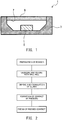
- a light-emitting device 1 of the present embodiment includes a box-shaped ceramic package (container) 3 formed of, for example, alumina; a light-emitting element 5 (e.g., LD) disposed in the interior of the container 3; and a plate-like optical wavelength conversion member 9 disposed so as to cover an opening 7 of the container 3.
- a box-shaped ceramic package (container) 3 formed of, for example, alumina
- a light-emitting element 5 e.g., LD
- a plate-like optical wavelength conversion member 9 disposed so as to cover an opening 7 of the container 3.
- the optical wavelength conversion member 9 emits fluorescence having a wavelength different from that of light emitted from the light-emitting element 5.
- the optical wavelength conversion member 9 converts the wavelength of blue light emitted from an LD, whereby the optical wavelength conversion member 9 as a whole emits white light to the outside (e.g., upward in FIG. 1 ).
- optical wavelength conversion member 9 will now be described.
- the optical wavelength conversion member 9 of the present embodiment is formed of a ceramic sintered body having a fluorescent phase containing fluorescent crystal grains (i.e., fluorescent phase grains) as a main component and a translucent phase containing translucent crystal grains (i.e., fluorescent phase grains) as a main component.
- the fluorescent phase grains have a composition represented by formula A 3 B 5 O 12 :Ce, and each of the element A and the element B is at least one element selected from the following element groups:
- a and B of the aforementioned chemical formula A 3 B 5 O 12 :Ce correspond to elements (different elements) forming a substance represented by formula A 3 B 5 O 12 :Ce wherein O is oxygen and Ce is cerium.
- the optical wavelength conversion member 9 the following relations are satisfied: 0.3 ⁇ a ⁇ 34 and 300 ⁇ m ⁇ y ⁇ 1,050 ⁇ m wherein a represents the ratio of the area of the translucent phase to the area of the fluorescent phase in a cross section of the optical wavelength conversion member 9, and y represents the interfacial length of the fluorescent phase in a predetermined region.
- the predetermined region corresponds to a unit area of 500 ⁇ m 2
- the interfacial length y is the total of interfacial lengths corresponding to the perimeter lengths of fluorescent phases in the unit area.
- x represents the ratio of the mean grain size r1 of the translucent phase grains to the mean grain size r2 of the fluorescent phase grains; the translucent phase grains have a mean grain size r1 of 0.2 ⁇ m to 6 ⁇ m; and the fluorescent phase grains have a mean grain size r2 of 0.1 ⁇ m to 4 ⁇ m.
- the ceramic sintered body contains a compound represented by formula A 3 B 5 O 12 :Ce in an amount of 3 vol.% to 70 vol.%.
- the Ce content of the compound represented by formula A 3 B 5 O 12 :Ce is 0.1 mol% to 1.0 mol% relative to the element A of the compound.
- the translucent phase grains have, for example, a composition of Al 2 O 3 .
- powder materials for the optical wavelength conversion member 9 i.e., ceramic sintered body
- the powder materials were prepared).
- the resultant granular product was then press-formed into a compact.
- the compact was then fired at a specific temperature for a specific period of time, to thereby prepare a ceramic sintered body.
- the ceramic sintered body may be produced by any process instead of the aforementioned press-forming process.
- the ceramic sintered body may be produced by a process involving formation of a sheet from the slurry, and firing of the sheet.
- the density of each ceramic sintered body sample was measured by the Archimedes method, and the measured density was converted into a relative density.
- the open porosity of each ceramic sintered body sample was measured by the method specified by JIS R1634.
- FIG. 3 is a schematic view of an example of an SEM image.
- off-white bright portions correspond to fluorescent phases
- dark (black) portions correspond to translucent phases.
- the area ST of translucent phases and the area SK of fluorescent phases were measured.
- the area ratio a of the area ST of translucent phases to the area SK of fluorescent phases i.e., ST/SK was determined through calculation.
- the aforementioned area was determined through processing of the SEM image with image analysis software (e.g., Winloof).
- image analysis software e.g., Winloof
- the area may be measured in a specific visual field region, and then the specific visual field region may be converted into a 500 ⁇ m 2 region for determination of the area ratio a.
- the specific visual field region may be converted into a 500 ⁇ m 2 region in the same manner as described above.
- FIG. 4 is a schematic view of an example of SEM image.
- bright portions correspond to fluorescent phase grains
- dark portions correspond to translucent phase grains.
- the intercept method was used to determine the mean crystal grain sizes (i.e., mean grain sizes) of fluorescent phase grains and translucent phase grains.
- mean grain size r2 of fluorescent phase grains and the mean grain size r1 of translucent phase grains were determined in all the five regions.
- the grain size ratio x was calculated from the mean grain size r2 of fluorescent phase grains and the mean grain size r1 of translucent phase grains by use of the following formula (1).
- Grain size ratio x the mean grain size r 1 of translucent phase grains / the mean grain size r 2 of fluorescent phase grains
- the interfacial length of each fluorescent phase was determined by use of the aforementioned image analysis software (e.g., Winloof) in each of the five regions. Thus, the interfacial length per fluorescent phase unit was determined. In a region including a plurality of fluorescent phases, the interfacial lengths of the fluorescent phases were summed. Thus, the interfacial lengths of all the fluorescent phases were determined in each region, and the interfacial lengths were summed (i.e., the total interfacial length was determined) in each region.
- the aforementioned image analysis software e.g., Winloof
- Each of the five regions has an area of 500 ⁇ m 2 .
- the total interfacial lengths were determined in the five regions and then averaged. The average value was defined as the interfacial length y.
- FIG. 3 illustrates an example of the interfacial length; i.e., the interfacial length per fluorescent phase unit.
- the length of a white annular line surrounding one fluorescent phase i.e., one off-white bright portion
- Illuminance was measured by means of an illuminometer. Specifically, each sample was processed into a shape of 13 mm ⁇ 13 mm ⁇ 0.2 mm (thickness). Blue LD light (wavelength: 465 nm) was focused to a width of 0.5 mm by means of a lens, and the processed sample was irradiated with the focused light. A spectroradiometer (CL-500A, manufactured by KONICA MINOLTA, INC.) was used to determine the illuminance of the light transmitting through the surface of the sample opposite the surface irradiated with the focused light.
- CL-500A manufactured by KONICA MINOLTA, INC.
- Illuminance (%) was evaluated by a value relative to that (taken as 100) of a YAG:Ce single-crystal body.
- Color unevenness i.e., variation in color
- a variation in chromaticity was evaluated through determination of a variation in chromaticity by means of an illuminometer.
- each sample was processed into a shape of 13 mm ⁇ 13 mm ⁇ 0.2 mm (thickness).
- Blue LD light (wavelength: 465 nm) was focused to a width of 0.5 mm by means of a lens, and the processed sample was irradiated with the focused light.
- a spectroradiometer (CL-500A, manufactured by KONICA MINOLTA, INC.) was used to determine the chromaticity of the light transmitting through the surface of the sample opposite the surface irradiated with the focused light.
- a 9 mm square center portion of the surface of each sample i.e., sample surface
- the light irradiation was performed on each region.
- a variation ( ⁇ X) in chromaticity (in X-direction) of the region was evaluated.
- variation ( ⁇ X) refers to the maximum deviation of chromaticity (in X-direction).
- a variation ⁇ X of less than 0.03 is preferred.
- chromaticity refers to a chromaticity indicated by the CIE-XYZ color system established by the International Commission on Illumination (CIE) in 1931. Specifically, the chromaticity is indicated by the xy chromaticity diagram (so-called CIE chromaticity diagram), wherein three primary colors of light are digitized and represented in an xy coordinate space.
- CIE International Commission on Illumination
- Each sample was processed into a shape of 13 mm ⁇ 13 mm ⁇ 0.2 mm (thickness).
- Blue LD light (wavelength: 465 nm) was focused to a width of 0.5 mm by means of a lens, and the processed sample was irradiated with the focused light.
- the light transmitting through the sample was focused by means of a lens, and the emission intensity (i.e., fluorescence intensity) was measured by means of a power sensor.
- the sample was irradiated with the light at a power density of 40 W/mm 2 .
- Fluorescence intensity (%) was evaluated by a value relative to that (taken as 100) of a YAG:Ce single-crystal body.
- Ceramic sintered body samples Nos. 1 to 9 (i.e., optical wavelength conversion members) were prepared under the conditions shown in Table 1.
- Al 2 O 3 powder (mean particle size: 0.2 ⁇ m), Y 2 O 3 powder (mean particle size: 1.2 ⁇ m), Gd 2 O 3 powder (mean particle size: 1.5 ⁇ m), and CeO 2 powder (mean particle size: 1.5 ⁇ m) were weighed as shown in Table 1.
- the A 3 B 5 O 12 :Ce content was fixed to 30 vol.% relative to the entire ceramic sintered body.
- the Ce content was fixed to 0.3 mol% relative to the element A.
- samples Nos. 1 and 2 the grinding was performed for more than 30 hours, and the firing was performed at 1,500°C for two to five hours.
- Example 1 can be prepared under the aforementioned conditions (different grinding times and firing conditions). For example, the longer the grinding time, the smaller the crystal grain size. When the firing temperature is elevated, crystal grains are grown; i.e., an increase in grain size. Thus, these conditions probably affect the interfacial length.
- samples Nos. 3 to 7 (area ratio a: 0.3 ⁇ a ⁇ 34, interfacial length y of fluorescent phase: 300 ⁇ m ⁇ y ⁇ 1,050 ⁇ m) exhibited good results; i.e., high fluorescence intensity, high illuminance, and reduced color unevenness.
- samples Nos. 1 and 2 (interfacial length y: more than 1,050 ⁇ m) exhibited low transmittance and low fluorescence intensity and illuminance.
- Samples Nos. 8 and 9 (interfacial length y: less than 300 ⁇ m) exhibited increased color unevenness due to very high transmittance of blue light.
- Ceramic sintered body samples Nos. 10 to 19 were prepared under the conditions shown in Table 1.
- Example 2 samples were prepared basically in the same manner as in Example 1.
- the grinding was performed for 16 hours, the firing was performed at 1,600°C for 10 hours, and the A 3 B 5 O 12 :Ce content was fixed to 1 vol.% to 80 vol.% relative to the entire ceramic sintered body.
- sample No. 10 (A 3 B 5 O 12 :Ce content: 1 vol.%) exhibited low fluorescence intensity due to insufficient fluorescence.
- Sample No. 19 (A 3 B 5 O 12 :Ce content: 80 vol.%) exhibited a considerable increase in temperature due to reduced thermal conduction, and low emission intensity due to temperature quenching.
- Ceramic sintered body samples Nos. 20 to 26 were prepared under the conditions shown in Table 1.
- Example 3 samples were prepared basically in the same manner as in Example 1.
- Example 2 The grinding time and the firing conditions were the same as those in Example 2.
- the A 3 B 5 O 12 :Ce content was fixed to 30 vol.% relative to the entire ceramic sintered body, and the Ce content was adjusted to 0.05 vol.% to 2.0 vol.%.
- samples Nos. 21 to 25 (Ce content: 0.1 vol.% to 1 vol.%) exhibited good results; i.e., high emission intensity, high illuminance, and reduced color unevenness.
- sample No. 20 (Ce content: less than 0.1 mol.%) exhibited low fluorescence intensity due to a small amount of emission center ion (i.e., insufficient fluorescence).
- Sample No. 26 (Ce content: more than 1 mol.%) exhibited low fluorescence intensity due to concentration quenching caused by excess Ce.
- Ceramic sintered body samples Nos. 27 to 30 were prepared under the conditions shown in Table 1.
- Example 3 samples were prepared basically in the same manner as in Example 1.
- Y 2 O 3 powder was used in combination with at least one of Lu 2 O 3 powder (mean particle size: 1.3 ⁇ m), Yb 2 O 3 powder (mean particle size: 1.5 ⁇ m), and Ga 2 O 3 powder (mean particle size: 1.3 ⁇ m).
- Lu 2 O 3 powder mean particle size: 1.3 ⁇ m
- Yb 2 O 3 powder mean particle size: 1.5 ⁇ m
- Ga 2 O 3 powder mean particle size: 1.3 ⁇ m
Landscapes
- Chemical & Material Sciences (AREA)
- Engineering & Computer Science (AREA)
- Ceramic Engineering (AREA)
- Organic Chemistry (AREA)
- Materials Engineering (AREA)
- Manufacturing & Machinery (AREA)
- Structural Engineering (AREA)
- Inorganic Chemistry (AREA)
- Physics & Mathematics (AREA)
- General Physics & Mathematics (AREA)
- Optics & Photonics (AREA)
- Luminescent Compositions (AREA)
- Led Device Packages (AREA)
Abstract
Description
- The present disclosure relates to an optical wavelength conversion member capable of converting light wavelength and used for, for example, a wavelength converter, a fluorescent material, a lighting apparatus, or a video apparatus, and to a light-emitting device.
- Recently, in head lamps and other lighting apparatuses, white light is generally achieved through wavelength conversion, by use of a phosphor, of blue light emitted from a light-emitting diode (LED) or a laser diode (LD).
- Such a phosphor is known to be used with a resin matrix, a glass matrix, or other matrices. However, in recent years, as the output of a light source increases, the phosphor is required to have higher durability. Thus, ceramic-based phosphors have received attention (see
Patent Documents 1 to 3). - A typically known ceramic phosphor is a Ce-activated garnet (A3B5O12) component, such as Y3Al5O12:Ce (YAG:Ce).
-
- Patent Document 1: Japanese Patent Application Laid-Open (kokai) No.
2014-132084 - Patent Document 2: Japanese Patent Application Laid-Open (kokai) No.
2015-34120 - Patent Document 3: Japanese Patent Application Laid-Open (kokai) No.
2015-149394 - The aforementioned conventional techniques have problems described below, and the problems are required to be solved.
- Specifically, the technique disclosed in
Patent Document 1 involves dispersion of CeAl11O18 in the phosphor matrix for preventing color unevenness due to Ce volatilization during a firing process. However, CeAl11O18 (i.e., a third component) absorbs light and thus causes reduction in emission intensity and illuminance. Although such a problem needs to be solved through, for example, considerably reducing the thickness of the fluorescent body, such a reduced thickness may cause another problem; i.e., impairment of the durability of the structure of the fluorescent body. - In the technique disclosed in
Patent Document 2, a ceramic member contains a rare earth element capable of forming an emission center ion in an amount of 1 to 50 mol%. However, an increase in emission center ion content may cause concentration quenching, resulting in low emission intensity or light flux. Thus, incorporation of a rare earth element in an amount within the aforementioned range causes very poor fluorescent properties and illuminance. - The technique disclosed in
Patent Document 3 involves employment of a structure in which a grain of YAG (which may serve as an emission component) is surrounded by grains of YAG not activated with Ce, for preventing reflection of excitation light at the interface between YAG and Al2O3 grains. However, this structure may cause temperature quenching, since the heat generated by YAG (i.e., a fluorescent component) is difficult to dissipate. - Thus, the aforementioned techniques encounter difficulty in achieving an optical wavelength conversion member exhibiting high illuminance, high fluorescence intensity, and reduced color unevenness.
- In view of the foregoing, an object of the present disclosure is to provide an optical wavelength conversion member and a light-emitting device, each of which exhibits high illuminance, high fluorescence intensity, and reduced color unevenness.
-
- (1) A first aspect of the present disclosure is directed to an optical wavelength conversion member comprising a ceramic sintered body having a fluorescent phase containing fluorescent crystal grains as a main component and a translucent phase containing translucent crystal grains as a main component.
- In the optical wavelength conversion member, the crystal grains of the fluorescent phase have a composition represented by formula A3B5O12:Ce, and each of the element A and the element B is at least one element selected from the following element groups:
- A: Sc, Y, and lanthanoids (except for Ce), and
- B: Al and Ga. In the optical wavelength conversion member, the following relations are satisfied:
0.3 < a < 34 and 300 µm < y < 1,050 µm, wherein a represents the ratio of the area of the translucent phase to the area of the fluorescent phase in a cross section of the optical wavelength conversion member, and y represents the interfacial length of the fluorescent phase. - In the first aspect, the ceramic sintered body basically has a garnet structure represented by A3B5O12:Ce containing at least one element selected from the aforementioned element groups.
- This structural property can achieve effective conversion of blue light into visible light.
- Particularly in the first aspect, the area ratio a of the translucent phase to the fluorescent phase in a cross section of the optical wavelength conversion member satisfies the following relation 0.3 < a < 34, and the interfacial length y of the fluorescent phase satisfies the following relation 300 µm < y < 1,050 µm. Thus, when the optical wavelength conversion member is irradiated with light, high illuminance and high fluorescence intensity are achieved, and color unevenness is reduced as shown in the Examples and other sections described hereinbelow.
- When the interfacial length y of the fluorescent phase is less than 300 µm; i.e., when the size of an aggregation of the fluorescent phase is large in a predetermined region (specifically, per specified unit area), or the amount of the fluorescent phase is small, optical diffusion is reduced at the interface between the fluorescent phase and the translucent phase, resulting in increased transmittance, illuminance, and fluorescence intensity. However, color unevenness occurs.
- Meanwhile, when the interfacial length y of the fluorescent phase exceeds 1,050 µm; i.e., when the size of an aggregation of the fluorescent phase is small in a predetermined region, optical diffusion increases at the interface between the fluorescent phase and the translucent phase, resulting in low transmittance and reduced color unevenness. However, illuminance and fluorescence intensity decrease.
- When the area ratio a is less than 0.3, the fluorescent phase is insufficient, and thus translucency is unsatisfactory, and illuminance and fluorescence intensity decrease. Meanwhile, when the area ratio a exceeds 34, the amount of the fluorescent component is insufficient, and thus satisfactory emission is not achieved.
- Notably, the optical wavelength conversion member according to the first aspect exhibits excellent heat resistance and durability.
(2) In a second aspect of the present disclosure, which is a specific embodiment of the first aspect, wherein the following relation is satisfied: 1.1 < x < 2.1, wherein x represents the ratio of the mean grain size r1 of crystal grains of the translucent phase to the mean grain size r2 of crystal grains of the fluorescent phase; the crystal grains of the translucent phase have a mean grain size r1 of 0.2 µm to 6 µm; and the crystal grains of the fluorescent phase have a mean grain size r2 of 0.1 µm to 4 µm. - When the aforementioned ratio x (i.e., the grain size ratio x) is less than 1.1, transmittance decreases, and blue light diffusion increases. Thus, color unevenness is reduced, but illuminance and fluorescence intensity decrease.
- Meanwhile, when the grain size ratio x exceeds 2.1, transmittance increases, and illuminance and fluorescence intensity increase, but color unevenness occurs.
- Therefore, the grain size ratio x preferably falls within the aforementioned range.
- When the crystal grains of the translucent phase have a mean grain size r1 of 0.2 µm to 6 µm, and the crystal grains of the fluorescent phase have a mean grain size r2 of 0.1 µm to 4 µm, the resultant ceramic phosphor exhibits high fluorescence intensity and illuminance and reduced color unevenness.
- When the crystal grains of the translucent phase have a mean grain size r1 of less than 0.2 µm, and the crystal grains of the fluorescent phase have a mean grain size r2 of less than 0.1 µm, blue light and yellow light diffusion increases, and thus color unevenness is reduced. However, the transmittances of blue light and yellow light are lowered, and fluorescence intensity and illuminance are also lowered.
- Meanwhile, when the crystal grains of the translucent phase have a mean grain size r1 of more than 6 µm, and the crystal grains of the fluorescent phase have a mean grain size r2 of more than 4 µm, transmittance increases, and fluorescence intensity and illuminance increase, but color unevenness increases.
- (3) In a third aspect of the present disclosure, which is a specific embodiment of the first or second aspect, wherein the crystal grains of the translucent phase have a composition of Al2O3.
This is an example of preferred composition of the crystal grains of the translucent phase. - (4) In a fourth aspect of the present disclosure, which is a specific embodiment of any one of the first to third aspects, wherein the ceramic sintered body contains a compound represented by formula A3B5O12:Ce in an amount of 3 vol.% to 70 vol.%.
When the A3B5O12:Ce content of the entire ceramic sintered body is 3 vol.% to 70 vol.%, the ceramic sintered body exhibits high illuminance and reduced color unevenness.
When the A3B5O12:Ce content is less than 3 vol.%, the amount of the fluorescent component is insufficient, resulting in unsatisfactory emission, whereas when the A3B5O12:Ce content exceeds 70 vol.%, the amount of the translucent phase is insufficient, resulting in unsatisfactory translucency and low illuminance and fluorescence intensity. - (5) In a fifth aspect of the present disclosure, which is a specific embodiment of any one of the first to fourth aspects, wherein the Ce content of the compound represented by formula A3B5O12:Ce is 0.1 mol% to 1.0 mol% relative to the element A of the compound.
When the Ce content of the compound represented by A3B5O12:Ce is 0.1 mol% to 1.0 mol% relative to the element A in the ceramic sintered body, the ceramic sintered body exhibits high illuminance and fluorescence intensity and reduced color unevenness.
When the Ce content is less than 0.1 mol%, the amount of the emission center ion is small, and the amount of the fluorescent component is insufficient, resulting in unsatisfactory emission, whereas when the Ce content exceeds 1.0 mol%, the amount of the emission center ion increases, and concentration quenching occurs, resulting in low fluorescence intensity and illuminance. - (6) A sixth aspect of the present disclosure is directed to a light-emitting device comprising an optical wavelength conversion member as recited in any one of the first to fifth aspects.
- The light (i.e., fluorescence) having a wavelength converted with the light-emitting device (specifically, the optical wavelength conversion member) according to the sixth aspect exhibits high fluorescence intensity and high color uniformity.
- The light-emitting device may include any known light-emitting element, such as LED or LD.
- The term "fluorescent phase" refers to a phase containing fluorescent crystal grains as a main component, and the term "translucent phase" refers to a phase containing translucent crystal grains (specifically, crystal grains having a composition different from that of the crystal grains of the fluorescent phase) as a main component.
- The term "main component" refers to a component which is present in the optical wavelength conversion member in the largest amount (i.e., volume). For example, the fluorescent phase may contain fluorescent crystal grains in an amount of 50 vol.% or more (preferably 90 vol.% or more). For example, the translucent phase may contain translucent crystal grains in an amount of 50 vol.% or more (preferably 90 vol.% or more) .
- The term "optical wavelength conversion member," which has the aforementioned characteristic features, is formed of a ceramic sintered body. Crystal grains or the grain boundary therebetween may contain an unavoidable impurity. The ceramic sintered body may contain the translucent phase and the translucent phase (i.e., fluorescent crystal grains and translucent crystal grains) in an amount of 50 vol.% or more (preferably 90 vol.% or more).
- The term "A3B5O12:Ce" refers to the case where a portion of the element A contained in A3B5O12 is substituted by Ce through formation of a solid solution. The compound having such a structure exhibits fluorescent properties.
- The term "interfacial length" refers to the total perimeter length of a portion forming one or more fluorescent phases in a predetermined region (specifically, a unit area of 500 µm2) in a cross section of the optical wavelength conversion member. For example, in the case where a plurality of independent fluorescent phases are present in a predetermined region, the interfacial length is the total of the perimeter lengths of the fluorescent phases.
-
- [
FIG. 1 ] Cross-sectional view of a light-emitting device in a thickness direction, the light-emitting device including an optical wavelength conversion member according to an embodiment. - [
FIG. 2 ] Explanatory view showing a production process for the optical wavelength conversion member according to the embodiment. - [
FIG. 3 ] Schematic view showing an SEM image of a cross section of the optical wavelength conversion member according to the embodiment; specifically, schematic view showing an SEM image of an unetched cross-sectional surface. - [
FIG. 4 ] Schematic view showing an SEM image of a cross section of the optical wavelength conversion member according to the embodiment; specifically, schematic view showing an SEM image of an etched cross-sectional surface. - [
FIG. 5 ] Explanatory view showing a method of determining color unevenness. - Next will be described an optical wavelength conversion member and a light-emitting device according to an embodiment of the present disclosure.
- Now will be described an optical wavelength conversion member and a light-emitting device according to the present embodiment.
- As illustrated in
FIG. 1 , a light-emittingdevice 1 of the present embodiment includes a box-shaped ceramic package (container) 3 formed of, for example, alumina; a light-emitting element 5 (e.g., LD) disposed in the interior of thecontainer 3; and a plate-like opticalwavelength conversion member 9 disposed so as to cover anopening 7 of thecontainer 3. - In the light-emitting
device 1, light emitted from the light-emittingelement 5 transmits through the translucent opticalwavelength conversion member 9, and the wavelength of a portion of the emitted light is converted in the interior of the opticalwavelength conversion member 9. Thus, the opticalwavelength conversion member 9 emits fluorescence having a wavelength different from that of light emitted from the light-emittingelement 5. - For example, the optical
wavelength conversion member 9 converts the wavelength of blue light emitted from an LD, whereby the opticalwavelength conversion member 9 as a whole emits white light to the outside (e.g., upward inFIG. 1 ). - The optical
wavelength conversion member 9 will now be described. - The optical
wavelength conversion member 9 of the present embodiment is formed of a ceramic sintered body having a fluorescent phase containing fluorescent crystal grains (i.e., fluorescent phase grains) as a main component and a translucent phase containing translucent crystal grains (i.e., fluorescent phase grains) as a main component. - In the optical
wavelength conversion member 9, the fluorescent phase grains have a composition represented by formula A3B5O12:Ce, and each of the element A and the element B is at least one element selected from the following element groups: - A: Sc, Y, and lanthanoids (except for Ce), and
- B: Al and Ga.
- A and B of the aforementioned chemical formula A3B5O12:Ce correspond to elements (different elements) forming a substance represented by formula A3B5O12:Ce wherein O is oxygen and Ce is cerium.
- In the optical
wavelength conversion member 9, the following relations are satisfied: 0.3 < a < 34 and 300 µm < y < 1,050 µm wherein a represents the ratio of the area of the translucent phase to the area of the fluorescent phase in a cross section of the opticalwavelength conversion member 9, and y represents the interfacial length of the fluorescent phase in a predetermined region. - The predetermined region corresponds to a unit area of 500 µm2, and the interfacial length y is the total of interfacial lengths corresponding to the perimeter lengths of fluorescent phases in the unit area.
- In addition, the following relation is satisfied: 1.1 < x < 2.1, wherein x represents the ratio of the mean grain size r1 of the translucent phase grains to the mean grain size r2 of the fluorescent phase grains; the translucent phase grains have a mean grain size r1 of 0.2 µm to 6 µm; and the fluorescent phase grains have a mean grain size r2 of 0.1 µm to 4 µm.
- In the optical
wavelength conversion member 9, the ceramic sintered body contains a compound represented by formula A3B5O12:Ce in an amount of 3 vol.% to 70 vol.%. - The Ce content of the compound represented by formula A3B5O12:Ce is 0.1 mol% to 1.0 mol% relative to the element A of the compound.
- The translucent phase grains have, for example, a composition of Al2O3.
- A schematic production process for the optical
wavelength conversion member 9 will now be briefly described with reference toFIG. 2 . - Firstly, powder materials for the optical wavelength conversion member 9 (i.e., ceramic sintered body) were weighed so as to satisfy the aforementioned embodiment (i.e., the powder materials were prepared).
- Subsequently, an organic solvent and a dispersant were added to the prepared powder materials, and these materials were ground and mixed in a ball mill, to thereby prepare a slurry.
- Subsequently, the slurry was dried and granulated.
- The resultant granular product was then press-formed into a compact.
- The compact was then fired at a specific temperature for a specific period of time, to thereby prepare a ceramic sintered body.
- The ceramic sintered body may be produced by any process instead of the aforementioned press-forming process. For example, the ceramic sintered body may be produced by a process involving formation of a sheet from the slurry, and firing of the sheet.
- The effects of the present embodiment will now be described.
- (1) In the present embodiment, the ceramic sintered body basically has a garnet structure represented by A3B5O12:Ce containing at least one element selected from the aforementioned element groups. This property can achieve effective conversion of blue light into visible light.
Particularly in the present embodiment, the area ratio a of the translucent phase to the fluorescent phase in a cross section of the opticalwavelength conversion member 9 satisfies the following relation 0.3 < a < 34, and the interfacial length y of the fluorescent phase satisfies the following relation 300 µm < y < 1,050 µm. Thus, when the opticalwavelength conversion member 9 is irradiated with light emitted from the light-emittingelement 5, high illuminance and high fluorescence intensity are achieved, and color unevenness is reduced. - (2) In the present embodiment, the grain size ratio x (i.e., the ratio of the mean grain size r1 of the translucent phase grains to the mean grain size r2 of the fluorescent phase grains) satisfies the relation 1.1 < x < 2.1; the crystal grains of the translucent phase have a mean grain size r1 of 0.2 µm to 6 µm; and the crystal grains of the fluorescent phase have a mean grain size r2 of 0.1 µm to 4 µm.
This characteristic feature achieves further high illuminance and fluorescence intensity and reduced color unevenness. - (3) In the present embodiment, the ceramic sintered body contains a compound represented by formula A3B5O12:Ce in an amount of 3 vol.% to 70 vol.%.
This characteristic feature achieves further high illuminance and fluorescence intensity and reduced color unevenness. - (4) In the present embodiment, the Ce content of the compound represented by formula A3B5O12:Ce is 0.1 mol% to 1.0 mol% relative to the element A of the compound.
This characteristic feature achieves further high illuminance and fluorescence intensity and reduced color unevenness. - (5) The light (i.e., fluorescence) having a wavelength converted with the light-emitting device 1 (specifically, the optical wavelength conversion member 9) of the present embodiment exhibits high fluorescence intensity. The light exhibits reduced color unevenness; i.e., high color uniformity.
- Specific examples of the aforementioned embodiment will next be described.
- There were prepared ceramic sintered body samples (Nos. 1 to 30) shown below in Table 1; i.e., samples of optical wavelength conversion members of Examples 1 to 5.
- Samples Nos. 3 to 7 and 11 to 30 fall within the scope of the present disclosure, and samples Nos. 1, 2, and 8 to 10 fall outside the scope of the present disclosure (Comparative Examples).
- Now will be described methods of evaluating the samples.
- The density of each ceramic sintered body sample was measured by the Archimedes method, and the measured density was converted into a relative density.
- The open porosity of each ceramic sintered body sample was measured by the method specified by JIS R1634.
- Each ceramic sintered body sample was sectioned, and the cross-sectional surface was subjected to mirror polishing. The polished surface was observed under a scanning electron microscope (SEM) at a magnification of 5,000, to thereby prepare an SEM image.
FIG. 3 is a schematic view of an example of an SEM image. InFIG. 3 , off-white bright portions correspond to fluorescent phases, and dark (black) portions correspond to translucent phases. - In a 500 µm2 region of the SEM image, the area ST of translucent phases and the area SK of fluorescent phases were measured. The area ratio a of the area ST of translucent phases to the area SK of fluorescent phases (i.e., ST/SK) was determined through calculation.
- The aforementioned area was determined through processing of the SEM image with image analysis software (e.g., Winloof). In an SEM image (×5,000), the area may be measured in a specific visual field region, and then the specific visual field region may be converted into a 500 µm2 region for determination of the area ratio a. For determination of the below-described interfacial length, the specific visual field region may be converted into a 500 µm2 region in the same manner as described above.
- Each ceramic sintered body sample was sectioned, and the cross-sectional surface was subjected to mirror polishing and subsequent thermal etching at 1,350°C. The etched surface was subjected to SEM observation, to thereby prepare x2,500 images (i.e., SEM images) at five positions of the ceramic sintered body.
FIG. 4 is a schematic view of an example of SEM image. InFIG. 4 , bright portions correspond to fluorescent phase grains, and dark portions correspond to translucent phase grains. - Five lines were drawn in a 20 µm square region of the SEM image at each of the aforementioned positions, and the intercept method was used to determine the mean crystal grain sizes (i.e., mean grain sizes) of fluorescent phase grains and translucent phase grains. Thus, the mean grain size r2 of fluorescent phase grains and the mean grain size r1 of translucent phase grains were determined in all the five regions.
- The grain size ratio x was calculated from the mean grain size r2 of fluorescent phase grains and the mean grain size r1 of translucent phase grains by use of the following formula (1).

- In the ×5,000 SEM image used for determination of the area ratio, the interfacial length of each fluorescent phase was determined by use of the aforementioned image analysis software (e.g., Winloof) in each of the five regions. Thus, the interfacial length per fluorescent phase unit was determined. In a region including a plurality of fluorescent phases, the interfacial lengths of the fluorescent phases were summed. Thus, the interfacial lengths of all the fluorescent phases were determined in each region, and the interfacial lengths were summed (i.e., the total interfacial length was determined) in each region.
- Each of the five regions has an area of 500 µm2. The total interfacial lengths were determined in the five regions and then averaged. The average value was defined as the interfacial length y.
-
FIG. 3 illustrates an example of the interfacial length; i.e., the interfacial length per fluorescent phase unit. InFIG. 3 , the length of a white annular line surrounding one fluorescent phase (i.e., one off-white bright portion) corresponds to the interfacial length per fluorescent phase unit. - Illuminance was measured by means of an illuminometer. Specifically, each sample was processed into a shape of 13 mm × 13 mm × 0.2 mm (thickness). Blue LD light (wavelength: 465 nm) was focused to a width of 0.5 mm by means of a lens, and the processed sample was irradiated with the focused light. A spectroradiometer (CL-500A, manufactured by KONICA MINOLTA, INC.) was used to determine the illuminance of the light transmitting through the surface of the sample opposite the surface irradiated with the focused light.
- Illuminance (%) was evaluated by a value relative to that (taken as 100) of a YAG:Ce single-crystal body.
- Color unevenness (i.e., variation in color) was evaluated through determination of a variation in chromaticity by means of an illuminometer.
- Specifically, each sample was processed into a shape of 13 mm × 13 mm × 0.2 mm (thickness). Blue LD light (wavelength: 465 nm) was focused to a width of 0.5 mm by means of a lens, and the processed sample was irradiated with the focused light. A spectroradiometer (CL-500A, manufactured by KONICA MINOLTA, INC.) was used to determine the chromaticity of the light transmitting through the surface of the sample opposite the surface irradiated with the focused light.
- As illustrated in
FIG. 5 , a 9 mm square center portion of the surface of each sample (i.e., sample surface) was divided into nine regions (at intervals of 3 mm), and the light irradiation was performed on each region. A variation (ΔX) in chromaticity (in X-direction) of the region was evaluated. As used herein, the term "variation (ΔX)" refers to the maximum deviation of chromaticity (in X-direction). A variation ΔX of less than 0.03 is preferred. - The term "chromaticity" as used herein refers to a chromaticity indicated by the CIE-XYZ color system established by the International Commission on Illumination (CIE) in 1931. Specifically, the chromaticity is indicated by the xy chromaticity diagram (so-called CIE chromaticity diagram), wherein three primary colors of light are digitized and represented in an xy coordinate space.
- Each sample was processed into a shape of 13 mm × 13 mm × 0.2 mm (thickness). Blue LD light (wavelength: 465 nm) was focused to a width of 0.5 mm by means of a lens, and the processed sample was irradiated with the focused light. The light transmitting through the sample was focused by means of a lens, and the emission intensity (i.e., fluorescence intensity) was measured by means of a power sensor. The sample was irradiated with the light at a power density of 40 W/mm2.
- Fluorescence intensity (%) was evaluated by a value relative to that (taken as 100) of a YAG:Ce single-crystal body.
- Next will be described a production method for each sample, and the results of evaluation of the sample.
- Ceramic sintered body samples Nos. 1 to 9 (i.e., optical wavelength conversion members) were prepared under the conditions shown in Table 1.
- Specifically, for preparation of each ceramic sintered body sample, Al2O3 powder (mean particle size: 0.2 µm), Y2O3 powder (mean particle size: 1.2 µm), Gd2O3 powder (mean particle size: 1.5 µm), and CeO2 powder (mean particle size: 1.5 µm) were weighed as shown in Table 1.
- The A3B5O12:Ce content was fixed to 30 vol.% relative to the entire ceramic sintered body. The Ce content was fixed to 0.3 mol% relative to the element A.
- These powders were added to a ball mill together with ethanol, and these materials were ground and mixed for 4 to 48 hours. The resultant slurry was dried and granulated, and the resultant granular product was press-formed into a compact. The compact was fired in air at 1,500 to 1,800°C for 2 to 10 hours.
- Specifically, in samples Nos. 1 and 2, the grinding was performed for more than 30 hours, and the firing was performed at 1,500°C for two to five hours.
- In samples Nos. 3 to 7, the grinding was performed for 16 hours, and the firing was performed at 1,500°C to 1,750°C for 10 hours.
- In samples Nos. 8 and 9, the grinding was performed for 16 hours and 4 hours, respectively, and the firing was performed at 1,800°C for 10 hours.
- The samples of Example 1 can be prepared under the aforementioned conditions (different grinding times and firing conditions). For example, the longer the grinding time, the smaller the crystal grain size. When the firing temperature is elevated, crystal grains are grown; i.e., an increase in grain size. Thus, these conditions probably affect the interfacial length.
- Subsequently, each ceramic sintered body sample produced in the aforementioned manner was evaluated by the aforementioned evaluation methods. The results are shown in Table 1.
- As shown in Table 1, samples Nos. 3 to 7 (area ratio a: 0.3 < a < 34, interfacial length y of fluorescent phase: 300 µm < y < 1,050 µm) exhibited good results; i.e., high fluorescence intensity, high illuminance, and reduced color unevenness.
- In contrast, samples Nos. 1 and 2 (interfacial length y: more than 1,050 µm) exhibited low transmittance and low fluorescence intensity and illuminance. Samples Nos. 8 and 9 (interfacial length y: less than 300 µm) exhibited increased color unevenness due to very high transmittance of blue light.
- Although not shown in Table 1, all the samples exhibited a relative density of 99% or more. Similarly, the samples of Examples 2 to 4 exhibited a relative density of 99% or more.
- Ceramic sintered body samples Nos. 10 to 19 were prepared under the conditions shown in Table 1.
- In Example 2, samples were prepared basically in the same manner as in Example 1.
- However, the grinding was performed for 16 hours, the firing was performed at 1,600°C for 10 hours, and the A3B5O12:Ce content was fixed to 1 vol.% to 80 vol.% relative to the entire ceramic sintered body.
- Each ceramic sintered body sample produced in the aforementioned manner was evaluated by the aforementioned evaluation methods. The results are shown in Table 1.
- As shown in Table 1, samples Nos. 11 to 18 (A3B5O12:Ce content: 3 vol.% to 70 vol.%) exhibited good results; i.e., high emission intensity and reduced color unevenness.
- In contrast, sample No. 10 (A3B5O12:Ce content: 1 vol.%) exhibited low fluorescence intensity due to insufficient fluorescence. Sample No. 19 (A3B5O12:Ce content: 80 vol.%) exhibited a considerable increase in temperature due to reduced thermal conduction, and low emission intensity due to temperature quenching.
- Ceramic sintered body samples Nos. 20 to 26 were prepared under the conditions shown in Table 1.
- In Example 3, samples were prepared basically in the same manner as in Example 1.
- However, the grinding time and the firing conditions were the same as those in Example 2. The A3B5O12:Ce content was fixed to 30 vol.% relative to the entire ceramic sintered body, and the Ce content was adjusted to 0.05 vol.% to 2.0 vol.%.
- Each ceramic sintered body sample produced in the aforementioned manner was evaluated by the aforementioned evaluation methods. The results are shown in Table 1.
- As shown in Table 1, samples Nos. 21 to 25 (Ce content: 0.1 vol.% to 1 vol.%) exhibited good results; i.e., high emission intensity, high illuminance, and reduced color unevenness.
- In contrast, sample No. 20 (Ce content: less than 0.1 mol.%) exhibited low fluorescence intensity due to a small amount of emission center ion (i.e., insufficient fluorescence). Sample No. 26 (Ce content: more than 1 mol.%) exhibited low fluorescence intensity due to concentration quenching caused by excess Ce.
- Ceramic sintered body samples Nos. 27 to 30 were prepared under the conditions shown in Table 1.
- In Example 3, samples were prepared basically in the same manner as in Example 1.
- However, Y2O3 powder was used in combination with at least one of Lu2O3 powder (mean particle size: 1.3 µm), Yb2O3 powder (mean particle size: 1.5 µm), and Ga2O3 powder (mean particle size: 1.3 µm). During mixing of the raw materials, the proportions of the raw materials were varied so that specific A3B5O12:Ce was synthesized. The grinding time and the firing conditions were the same as those in Example 2.
- Each ceramic sintered body sample produced in the aforementioned manner was evaluated by the aforementioned evaluation methods. The results are shown in Table 1.
- As shown in Table 1, all the ceramic sintered body samples (Nos. 27 to 30) exhibited good results in terms of illuminance, fluorescence intensity, and color unevenness.
[Table 1] No. A B A3B5O12:Ce content (vol%) Ce content (mol%) Open porosity (%) Area ratio (translucent phase/fluorescent phase) translucant phase mean grain size (µm) A3B5O12:Ce mean grain size (µm) Grain size ratio of translucent phase/fluorescent phase A3B5O12:Ce interfacial length (µm) Illuminance (%) Color unevenness (ΔX) Fluorescence intensity (%) Example 1 1 Y,Gd Al 30 0.3 0.4 2.33 0.11 0.1 1.1 1070 78 0.0006 83 2 Y,Gd Al 30 0.3 0.02 2.38 0.24 0.22 1.09 1056.07 80 0.0007 85 3 Y,Gd Al 30 0.3 0.02 2.32 0.32 0.24 1.33 823.41 101 0.0008 100 4 Y,Gd Al 30 0.3 0.01 2.31 0.98 0.58 1.69 802.19 120 0.001 110 5 Y,Gd Al 30 0.3 0 2.28 1.44 0.91 1.58 749.00 125 0.0016 114 6 Y,Gd Al 30 0.3 0.01 2.44 1.87 1.09 1.72 616.00 130 0.0019 125 7 Y,Gd Al 30 0.3 0.02 2.39 3.6 2.2 1.64 484.00 124 0.0024 120 8 Y,Gd Al 30 0.3 0.02 2.39 6.2 2.9 2.14 294.56 95 0.0032 95 9 Y,Gd Al 30 0.3 0.2 2.32 9 4.1 2.20 275.00 93 0.0045 89 Example 2 10 Y,Gd Al 1 0.3 0.01 81.64 1.1 0.51 2.16 817.04 78 0.004 80.0 11 Y,Gd Al 3 0.3 0.02 32.67 1.08 0.52 2.08 814.92 100 0.0026 100.0 12 Y,Gd Al 5 0.3 0.02 17.98 1.07 0.52 2.06 814.92 113 0.0022 103.0 13 Y,Gd Al 10 0.3 0.01 8.79 1.02 0.55 1.85 808.56 118 0.0015 105.0 14 Y,Gd Al 30 0.3 0.02 2.31 0.98 0.58 1.69 802.19 120 0.001 110 15 Y,Gd Al 40 0.3 0.01 1.49 0.95 0.62 1.53 793.71 110 0.00095 118.0 16 Y,Gd Al 50 0.3 0.02 1.00 0.9 0.67 1.34 783.10 108 0.00088 120.0 17 Y,Gd Al 60 0.3 0 0.66 0.88 0.72 1.22 772.50 106 0.00085 124.0 18 Y,Gd Al 70 0.3 0 0.43 0.87 0.75 1.16 766.13 103 0.00084 128.0 19 Y,Gd Al 80 0.3 0.01 0.25 0.85 0.78 1.09 759.77 84 0.0008 130.0 Example 3 20 Y,Gd Al 30 0.05 0.01 2.32 0.6 0.58 1.03 812.80 80 0.0024 82 21 Y,Gd Al 30 0.1 0.01 2.37 0.92 0.54 1.70 810.68 105 0.0012 100 22 Y,Gd Al 30 0.3 0.01 2.31 0.98 0.58 1.69 802.19 120 0.001 110 23 Y,Gd Al 30 0.5 0 2.28 0.97 0.57 1.70 804.32 123 0.0011 115 24 Y,Gd Al 30 0.7 0.01 2.36 0.97 0.56 1.73 806.44 110 0.0015 105 25 Y,Gd Al 30 1 0.02 2.37 0.97 0.55 1.76 808.56 104 0.0016 101 26 Y,Gd Al 30 2 0.02 2.35 0.97 0.88 1.10 806.44 90 0.0014 92 Example 4 27 Lu Al 30 0.3 0.01 2.37 1.36 0.92 1.48 762.00 130 0.0015 120 28 Lu Al,Ga 30 0.3 0 2.26 1.41 0.94 1.50 753.00 124 0.0012 115 29 Yb Al 30 0.3 0.03 2.39 1.51 1.02 1.48 744.00 120 0.0011 114 30 Yb Al,Ga 30 0.3 0 2.27 1.46 1.05 1.39 780.00 140 0.0012 105 - Needless to say, the present disclosure is not limited to the aforementioned embodiment, but may be implemented in various other forms without departing from the scope of the present invention.
- (1) For example, the aforementioned embodiment employs an air firing process for the preparation of a sample. However, a hot pressing process, a vacuum firing process, a reducing-atmosphere firing process, an HIP process, or any combination of these processes may be used for the preparation of a sample having the same properties as those described in the embodiment.
- (2) The aforementioned optical wavelength conversion member or light-emitting device can be used for various applications, including fluorescent bodies, optical wavelength conversion apparatuses, head lamps, lighting apparatuses, and optical apparatuses (e.g., projectors).
- (3) No particular limitation is imposed on the light-emitting element used for the light-emitting device. The light-emitting element may be any well known one, such as LED or LD.
- (4) In the aforementioned embodiment, the function of a single component may be shared by a plurality of components, or a single component may exert the functions of a plurality of components. Some of the components in the aforementioned embodiment may be omitted. At least some of the components in the aforementioned embodiment may be, for example, added to or replaced with components in another embodiment. Embodiments of the present disclosure encompass any form included in technical ideas specified by the appended claims.
- 1: light-emitting device; 5: light-emitting element; and 9: optical wavelength conversion member
Claims (6)
- An optical wavelength conversion member comprising a ceramic sintered body having a fluorescent phase containing fluorescent crystal grains as a main component and a translucent phase containing translucent crystal grains as a main component, wherein
the crystal grains of the fluorescent phase have a composition represented by formula A3B5O12:Ce, and each of the element A and the element B is at least one element selected from the following element groups:A: Sc, Y, and lanthanoids (except for Ce), andB: Al and Ga; andthe following relations are satisfied:
- An optical wavelength conversion member according to claim 1, wherein the following relation is satisfied: 1.1 < x < 2.1, wherein x represents the ratio of the mean grain size r1 of crystal grains of the translucent phase to the mean grain size r2 of crystal grains of the fluorescent phase; the crystal grains of the translucent phase have a mean grain size r1 of 0.2 µm to 6 µm; and the crystal grains of the fluorescent phase have a mean grain size r2 of 0.1 µm to 4 µm.
- An optical wavelength conversion member according to claim 1 or 2, wherein the crystal grains of the translucent phase have a composition of Al2O3.
- An optical wavelength conversion member according to any one of claims 1 to 3, wherein the ceramic sintered body contains a compound represented by formula A3B5O12:Ce in an amount of 3 vol.% to 70 vol.%.
- An optical wavelength conversion member according to any one of claims 1 to 4, wherein the Ce content of the compound represented by formula A3B5O12:Ce is 0.1 mol% to 1.0 mol% relative to the element A of the compound.
- A light-emitting device comprising an optical wavelength conversion member as recited in any one of claims 1 to 5.
Applications Claiming Priority (6)
| Application Number | Priority Date | Filing Date | Title |
|---|---|---|---|
| JP2016211843 | 2016-10-28 | ||
| JP2016215303A JP6486315B2 (en) | 2016-11-02 | 2016-11-02 | Light wavelength conversion member and light emitting device |
| JP2017015653 | 2017-01-31 | ||
| JP2017100204 | 2017-05-19 | ||
| JP2017148393A JP6499237B2 (en) | 2017-07-31 | 2017-07-31 | Light wavelength conversion member and light emitting device |
| PCT/JP2017/037920 WO2018079421A1 (en) | 2016-10-28 | 2017-10-20 | Optical wavelength conversion member and light-emitting device |
Publications (3)
| Publication Number | Publication Date |
|---|---|
| EP3534193A1 true EP3534193A1 (en) | 2019-09-04 |
| EP3534193A4 EP3534193A4 (en) | 2020-05-13 |
| EP3534193B1 EP3534193B1 (en) | 2021-12-22 |
Family
ID=62023459
Family Applications (1)
| Application Number | Title | Priority Date | Filing Date |
|---|---|---|---|
| EP17865959.5A Active EP3534193B1 (en) | 2016-10-28 | 2017-10-20 | Optical wavelength conversion member and light-emitting device |
Country Status (6)
| Country | Link |
|---|---|
| US (1) | US10727378B2 (en) |
| EP (1) | EP3534193B1 (en) |
| KR (1) | KR102229730B1 (en) |
| CN (1) | CN109923446B (en) |
| TW (1) | TWI668295B (en) |
| WO (1) | WO2018079421A1 (en) |
Cited By (1)
| Publication number | Priority date | Publication date | Assignee | Title |
|---|---|---|---|---|
| EP3832360A4 (en) * | 2018-07-31 | 2022-04-20 | NGK Spark Plug Co., Ltd. | Light wavelength conversion member and light-emitting device |
Families Citing this family (7)
| Publication number | Priority date | Publication date | Assignee | Title |
|---|---|---|---|---|
| JP6725774B2 (en) * | 2018-07-11 | 2020-07-22 | 日本特殊陶業株式会社 | Light wavelength conversion member and light emitting device |
| TWI802899B (en) * | 2020-06-08 | 2023-05-21 | 日商日本特殊陶業股份有限公司 | Phosphor plate, wavelength conversion member, and light source device |
| WO2021251251A1 (en) * | 2020-06-08 | 2021-12-16 | 日本特殊陶業株式会社 | Fluorescent plate, wavelength conversion member, and light source device |
| JP7617364B2 (en) | 2020-08-07 | 2025-01-20 | 日亜化学工業株式会社 | Rare earth aluminate sintered body and method for producing same |
| EP4328207A1 (en) * | 2022-08-24 | 2024-02-28 | Nichia Corporation | Sintered body and method for producing sintered body |
| US20240186464A1 (en) | 2022-12-02 | 2024-06-06 | Ams-Osram International Gmbh | Converter and method for producing the same |
| CN119371181A (en) * | 2023-07-20 | 2025-01-28 | 深圳市绎立锐光科技开发有限公司 | Luminescent ceramic, preparation method, wavelength conversion device and luminescent device |
Family Cites Families (23)
| Publication number | Priority date | Publication date | Assignee | Title |
|---|---|---|---|---|
| JP3904874B2 (en) * | 2001-10-03 | 2007-04-11 | 京セラ株式会社 | Components for semiconductor manufacturing equipment |
| DE10361661A1 (en) * | 2003-07-14 | 2005-03-17 | Osram Opto Semiconductors Gmbh | Light-emitting component has luminescence conversion element, filter element with nano-particles that selectively reduce radiation intensity of unwanted radiation spectral sub-region(s) by absorption |
| EP1760794B1 (en) * | 2004-06-24 | 2014-01-15 | Ube Industries, Ltd. | White light emitting diode device |
| JP4513541B2 (en) * | 2004-12-17 | 2010-07-28 | 宇部興産株式会社 | Light emitting device using ceramic composite for light conversion |
| JP5490407B2 (en) | 2005-03-14 | 2014-05-14 | コーニンクレッカ フィリップス エヌ ヴェ | Phosphor having a polycrystalline ceramic structure, and light emitting device having the phosphor |
| US8093799B2 (en) * | 2006-09-25 | 2012-01-10 | Ube Industries, Ltd. | Ceramic composite for phototransformation and light emitting device using the same |
| DE102007010719A1 (en) * | 2007-03-06 | 2008-09-11 | Merck Patent Gmbh | Phosphors consisting of doped garnets for pcLEDs |
| JP5650885B2 (en) | 2008-12-27 | 2015-01-07 | 日亜化学工業株式会社 | Wavelength conversion sintered body, light emitting device using the same, and method for producing wavelength conversion sintered body |
| KR101013146B1 (en) * | 2010-02-16 | 2011-02-10 | 충남대학교산학협력단 | Rapid Solid-phase Synthesis of Yttrium Aluminum Garnet Yellow-emitting Phosphors |
| CN102947417B (en) * | 2010-03-31 | 2015-02-25 | 宇部兴产株式会社 | Ceramic composites for light conversion, process for production thereof, and light-emitting devices provided with same |
| JP5088977B2 (en) * | 2010-08-18 | 2012-12-05 | コバレントマテリアル株式会社 | Ceramic composite |
| EP2607449B1 (en) * | 2011-12-22 | 2014-04-02 | Shin-Etsu Chemical Co., Ltd. | Preparation of yttrium-cerium-aluminum garnet phosphor |
| CN104169392B (en) * | 2012-03-15 | 2016-06-22 | 株式会社东芝 | Solid scintillator, radiation detector and radiation inspecting apparatus |
| EP2832816B1 (en) | 2012-03-30 | 2016-01-20 | Ube Industries, Ltd. | Ceramic complex for light conversion and light-emitting device using same |
| JP2013227481A (en) | 2012-03-30 | 2013-11-07 | Covalent Materials Corp | Ceramic composite |
| JP5740017B2 (en) | 2012-03-30 | 2015-06-24 | コバレントマテリアル株式会社 | Ceramic composite |
| JP6241940B2 (en) | 2013-07-12 | 2017-12-06 | クアーズテック株式会社 | Alumina ceramic member and method for producing alumina ceramic member |
| JP6430123B2 (en) | 2014-02-06 | 2018-11-28 | スタンレー電気株式会社 | Wavelength converter and light emitting device using the same |
| MY177277A (en) * | 2014-03-03 | 2020-09-10 | Covalent Mat Corporation | Wavelength converting member |
| JP5862841B1 (en) | 2014-03-18 | 2016-02-16 | 宇部興産株式会社 | CERAMIC COMPOSITE MATERIAL FOR LIGHT CONVERSION, ITS MANUFACTURING METHOD, AND LIGHT EMITTING DEVICE EQUIPPED WITH THE SAME |
| EP3249026B1 (en) * | 2015-01-21 | 2023-11-29 | Mitsubishi Chemical Corporation | Sintered phosphor, light emitting device, illumination device, vehicle headlamp, and method for manufacturing sintered phosphor |
| JP6492824B2 (en) * | 2015-03-18 | 2019-04-03 | 宇部興産株式会社 | Ceramic composite material for light conversion and manufacturing method thereof |
| JP7056553B2 (en) * | 2016-03-29 | 2022-04-19 | 三菱ケミカル株式会社 | Fluorescent material, light emitting device, lighting device and image display device |
-
2017
- 2017-10-20 EP EP17865959.5A patent/EP3534193B1/en active Active
- 2017-10-20 KR KR1020197011086A patent/KR102229730B1/en active Active
- 2017-10-20 US US16/342,390 patent/US10727378B2/en active Active
- 2017-10-20 WO PCT/JP2017/037920 patent/WO2018079421A1/en not_active Ceased
- 2017-10-20 CN CN201780066919.2A patent/CN109923446B/en active Active
- 2017-10-27 TW TW106137049A patent/TWI668295B/en active
Cited By (2)
| Publication number | Priority date | Publication date | Assignee | Title |
|---|---|---|---|---|
| EP3832360A4 (en) * | 2018-07-31 | 2022-04-20 | NGK Spark Plug Co., Ltd. | Light wavelength conversion member and light-emitting device |
| US11945987B2 (en) | 2018-07-31 | 2024-04-02 | Niterra Co., Ltd. | Light wavelength conversion member and light-emitting device |
Also Published As
| Publication number | Publication date |
|---|---|
| KR20190053240A (en) | 2019-05-17 |
| CN109923446B (en) | 2021-05-18 |
| TW201821594A (en) | 2018-06-16 |
| KR102229730B1 (en) | 2021-03-18 |
| US20190259918A1 (en) | 2019-08-22 |
| CN109923446A (en) | 2019-06-21 |
| EP3534193B1 (en) | 2021-12-22 |
| WO2018079421A1 (en) | 2018-05-03 |
| TWI668295B (en) | 2019-08-11 |
| EP3534193A4 (en) | 2020-05-13 |
| US10727378B2 (en) | 2020-07-28 |
Similar Documents
| Publication | Publication Date | Title |
|---|---|---|
| EP3534193B1 (en) | Optical wavelength conversion member and light-emitting device | |
| EP3534192B1 (en) | Light wavelength conversion member and light emission device | |
| EP3249026A1 (en) | Sintered phosphor, light emitting device, illumination device, vehicle headlamp, and method for manufacturing sintered phosphor | |
| EP3492556A1 (en) | Sintered phosphor, light-emitting device, lighting device and vehicle indicator lamp | |
| JP7244644B2 (en) | Manufacturing method of ceramic converter element, ceramic converter element, and optoelectronic component | |
| EP3121246A1 (en) | Ceramic composite material for optical conversion, production method therefor, and light-emitting device provided with same | |
| KR102307670B1 (en) | Optical wavelength conversion member and light emitting device | |
| EP3822671B1 (en) | Optical wavelength conversion member and light-emitting device | |
| JP6499237B2 (en) | Light wavelength conversion member and light emitting device | |
| TW201809223A (en) | Red phosphor and manufacturing method thereof, and white light source, lighting device and display device using same | |
| US11512247B2 (en) | Phosphor plate | |
| EP3832360A1 (en) | Light wavelength conversion member and light-emitting device | |
| KR20170093320A (en) | Phosphor plate with light-diffusing material | |
| EP4328207A1 (en) | Sintered body and method for producing sintered body | |
| JP2022104527A (en) | Phosphor plate |
Legal Events
| Date | Code | Title | Description |
|---|---|---|---|
| STAA | Information on the status of an ep patent application or granted ep patent |
Free format text: STATUS: THE INTERNATIONAL PUBLICATION HAS BEEN MADE |
|
| PUAI | Public reference made under article 153(3) epc to a published international application that has entered the european phase |
Free format text: ORIGINAL CODE: 0009012 |
|
| STAA | Information on the status of an ep patent application or granted ep patent |
Free format text: STATUS: REQUEST FOR EXAMINATION WAS MADE |
|
| 17P | Request for examination filed |
Effective date: 20190417 |
|
| AK | Designated contracting states |
Kind code of ref document: A1 Designated state(s): AL AT BE BG CH CY CZ DE DK EE ES FI FR GB GR HR HU IE IS IT LI LT LU LV MC MK MT NL NO PL PT RO RS SE SI SK SM TR |
|
| AX | Request for extension of the european patent |
Extension state: BA ME |
|
| DAV | Request for validation of the european patent (deleted) | ||
| DAX | Request for extension of the european patent (deleted) | ||
| A4 | Supplementary search report drawn up and despatched |
Effective date: 20200414 |
|
| RIC1 | Information provided on ipc code assigned before grant |
Ipc: C04B 35/01 20060101ALI20200406BHEP Ipc: C09K 11/77 20060101ALI20200406BHEP Ipc: C04B 35/44 20060101ALI20200406BHEP Ipc: G02B 5/20 20060101AFI20200406BHEP Ipc: H01L 33/50 20100101ALI20200406BHEP Ipc: C04B 35/64 20060101ALI20200406BHEP Ipc: C09K 11/80 20060101ALI20200406BHEP Ipc: C04B 35/50 20060101ALI20200406BHEP Ipc: C04B 35/626 20060101ALI20200406BHEP |
|
| STAA | Information on the status of an ep patent application or granted ep patent |
Free format text: STATUS: EXAMINATION IS IN PROGRESS |
|
| 17Q | First examination report despatched |
Effective date: 20201130 |
|
| GRAP | Despatch of communication of intention to grant a patent |
Free format text: ORIGINAL CODE: EPIDOSNIGR1 |
|
| STAA | Information on the status of an ep patent application or granted ep patent |
Free format text: STATUS: GRANT OF PATENT IS INTENDED |
|
| INTG | Intention to grant announced |
Effective date: 20211004 |
|
| GRAS | Grant fee paid |
Free format text: ORIGINAL CODE: EPIDOSNIGR3 |
|
| GRAA | (expected) grant |
Free format text: ORIGINAL CODE: 0009210 |
|
| STAA | Information on the status of an ep patent application or granted ep patent |
Free format text: STATUS: THE PATENT HAS BEEN GRANTED |
|
| AK | Designated contracting states |
Kind code of ref document: B1 Designated state(s): AL AT BE BG CH CY CZ DE DK EE ES FI FR GB GR HR HU IE IS IT LI LT LU LV MC MK MT NL NO PL PT RO RS SE SI SK SM TR |
|
| REG | Reference to a national code |
Ref country code: GB Ref legal event code: FG4D |
|
| REG | Reference to a national code |
Ref country code: CH Ref legal event code: EP |
|
| REG | Reference to a national code |
Ref country code: DE Ref legal event code: R096 Ref document number: 602017051388 Country of ref document: DE |
|
| REG | Reference to a national code |
Ref country code: AT Ref legal event code: REF Ref document number: 1457421 Country of ref document: AT Kind code of ref document: T Effective date: 20220115 |
|
| REG | Reference to a national code |
Ref country code: IE Ref legal event code: FG4D |
|
| REG | Reference to a national code |
Ref country code: NL Ref legal event code: FP |
|
| REG | Reference to a national code |
Ref country code: LT Ref legal event code: MG9D |
|
| PG25 | Lapsed in a contracting state [announced via postgrant information from national office to epo] |
Ref country code: RS Free format text: LAPSE BECAUSE OF FAILURE TO SUBMIT A TRANSLATION OF THE DESCRIPTION OR TO PAY THE FEE WITHIN THE PRESCRIBED TIME-LIMIT Effective date: 20211222 Ref country code: LT Free format text: LAPSE BECAUSE OF FAILURE TO SUBMIT A TRANSLATION OF THE DESCRIPTION OR TO PAY THE FEE WITHIN THE PRESCRIBED TIME-LIMIT Effective date: 20211222 Ref country code: FI Free format text: LAPSE BECAUSE OF FAILURE TO SUBMIT A TRANSLATION OF THE DESCRIPTION OR TO PAY THE FEE WITHIN THE PRESCRIBED TIME-LIMIT Effective date: 20211222 Ref country code: BG Free format text: LAPSE BECAUSE OF FAILURE TO SUBMIT A TRANSLATION OF THE DESCRIPTION OR TO PAY THE FEE WITHIN THE PRESCRIBED TIME-LIMIT Effective date: 20220322 |
|
| REG | Reference to a national code |
Ref country code: AT Ref legal event code: MK05 Ref document number: 1457421 Country of ref document: AT Kind code of ref document: T Effective date: 20211222 |
|
| PG25 | Lapsed in a contracting state [announced via postgrant information from national office to epo] |
Ref country code: SE Free format text: LAPSE BECAUSE OF FAILURE TO SUBMIT A TRANSLATION OF THE DESCRIPTION OR TO PAY THE FEE WITHIN THE PRESCRIBED TIME-LIMIT Effective date: 20211222 Ref country code: NO Free format text: LAPSE BECAUSE OF FAILURE TO SUBMIT A TRANSLATION OF THE DESCRIPTION OR TO PAY THE FEE WITHIN THE PRESCRIBED TIME-LIMIT Effective date: 20220322 Ref country code: LV Free format text: LAPSE BECAUSE OF FAILURE TO SUBMIT A TRANSLATION OF THE DESCRIPTION OR TO PAY THE FEE WITHIN THE PRESCRIBED TIME-LIMIT Effective date: 20211222 Ref country code: HR Free format text: LAPSE BECAUSE OF FAILURE TO SUBMIT A TRANSLATION OF THE DESCRIPTION OR TO PAY THE FEE WITHIN THE PRESCRIBED TIME-LIMIT Effective date: 20211222 Ref country code: GR Free format text: LAPSE BECAUSE OF FAILURE TO SUBMIT A TRANSLATION OF THE DESCRIPTION OR TO PAY THE FEE WITHIN THE PRESCRIBED TIME-LIMIT Effective date: 20220323 |
|
| PG25 | Lapsed in a contracting state [announced via postgrant information from national office to epo] |
Ref country code: SM Free format text: LAPSE BECAUSE OF FAILURE TO SUBMIT A TRANSLATION OF THE DESCRIPTION OR TO PAY THE FEE WITHIN THE PRESCRIBED TIME-LIMIT Effective date: 20211222 Ref country code: SK Free format text: LAPSE BECAUSE OF FAILURE TO SUBMIT A TRANSLATION OF THE DESCRIPTION OR TO PAY THE FEE WITHIN THE PRESCRIBED TIME-LIMIT Effective date: 20211222 Ref country code: RO Free format text: LAPSE BECAUSE OF FAILURE TO SUBMIT A TRANSLATION OF THE DESCRIPTION OR TO PAY THE FEE WITHIN THE PRESCRIBED TIME-LIMIT Effective date: 20211222 Ref country code: PT Free format text: LAPSE BECAUSE OF FAILURE TO SUBMIT A TRANSLATION OF THE DESCRIPTION OR TO PAY THE FEE WITHIN THE PRESCRIBED TIME-LIMIT Effective date: 20220422 Ref country code: ES Free format text: LAPSE BECAUSE OF FAILURE TO SUBMIT A TRANSLATION OF THE DESCRIPTION OR TO PAY THE FEE WITHIN THE PRESCRIBED TIME-LIMIT Effective date: 20211222 Ref country code: EE Free format text: LAPSE BECAUSE OF FAILURE TO SUBMIT A TRANSLATION OF THE DESCRIPTION OR TO PAY THE FEE WITHIN THE PRESCRIBED TIME-LIMIT Effective date: 20211222 Ref country code: CZ Free format text: LAPSE BECAUSE OF FAILURE TO SUBMIT A TRANSLATION OF THE DESCRIPTION OR TO PAY THE FEE WITHIN THE PRESCRIBED TIME-LIMIT Effective date: 20211222 |
|
| PG25 | Lapsed in a contracting state [announced via postgrant information from national office to epo] |
Ref country code: PL Free format text: LAPSE BECAUSE OF FAILURE TO SUBMIT A TRANSLATION OF THE DESCRIPTION OR TO PAY THE FEE WITHIN THE PRESCRIBED TIME-LIMIT Effective date: 20211222 Ref country code: AT Free format text: LAPSE BECAUSE OF FAILURE TO SUBMIT A TRANSLATION OF THE DESCRIPTION OR TO PAY THE FEE WITHIN THE PRESCRIBED TIME-LIMIT Effective date: 20211222 |
|
| REG | Reference to a national code |
Ref country code: DE Ref legal event code: R097 Ref document number: 602017051388 Country of ref document: DE |
|
| PG25 | Lapsed in a contracting state [announced via postgrant information from national office to epo] |
Ref country code: IS Free format text: LAPSE BECAUSE OF FAILURE TO SUBMIT A TRANSLATION OF THE DESCRIPTION OR TO PAY THE FEE WITHIN THE PRESCRIBED TIME-LIMIT Effective date: 20220422 |
|
| PLBE | No opposition filed within time limit |
Free format text: ORIGINAL CODE: 0009261 |
|
| STAA | Information on the status of an ep patent application or granted ep patent |
Free format text: STATUS: NO OPPOSITION FILED WITHIN TIME LIMIT |
|
| PG25 | Lapsed in a contracting state [announced via postgrant information from national office to epo] |
Ref country code: DK Free format text: LAPSE BECAUSE OF FAILURE TO SUBMIT A TRANSLATION OF THE DESCRIPTION OR TO PAY THE FEE WITHIN THE PRESCRIBED TIME-LIMIT Effective date: 20211222 Ref country code: AL Free format text: LAPSE BECAUSE OF FAILURE TO SUBMIT A TRANSLATION OF THE DESCRIPTION OR TO PAY THE FEE WITHIN THE PRESCRIBED TIME-LIMIT Effective date: 20211222 |
|
| 26N | No opposition filed |
Effective date: 20220923 |
|
| PG25 | Lapsed in a contracting state [announced via postgrant information from national office to epo] |
Ref country code: SI Free format text: LAPSE BECAUSE OF FAILURE TO SUBMIT A TRANSLATION OF THE DESCRIPTION OR TO PAY THE FEE WITHIN THE PRESCRIBED TIME-LIMIT Effective date: 20211222 |
|
| PG25 | Lapsed in a contracting state [announced via postgrant information from national office to epo] |
Ref country code: MC Free format text: LAPSE BECAUSE OF FAILURE TO SUBMIT A TRANSLATION OF THE DESCRIPTION OR TO PAY THE FEE WITHIN THE PRESCRIBED TIME-LIMIT Effective date: 20211222 Ref country code: IT Free format text: LAPSE BECAUSE OF FAILURE TO SUBMIT A TRANSLATION OF THE DESCRIPTION OR TO PAY THE FEE WITHIN THE PRESCRIBED TIME-LIMIT Effective date: 20211222 |
|
| REG | Reference to a national code |
Ref country code: CH Ref legal event code: PL |
|
| REG | Reference to a national code |
Ref country code: BE Ref legal event code: MM Effective date: 20221031 |
|
| GBPC | Gb: european patent ceased through non-payment of renewal fee |
Effective date: 20221020 |
|
| PG25 | Lapsed in a contracting state [announced via postgrant information from national office to epo] |
Ref country code: LU Free format text: LAPSE BECAUSE OF NON-PAYMENT OF DUE FEES Effective date: 20221020 |
|
| REG | Reference to a national code |
Ref country code: NL Ref legal event code: HC Owner name: NITERRA CO., LTD.; JP Free format text: DETAILS ASSIGNMENT: CHANGE OF OWNER(S), CHANGE OF OWNER(S) NAME; FORMER OWNER NAME: NGK SPARK PLUG CO., LTD. Effective date: 20230705 |
|
| PG25 | Lapsed in a contracting state [announced via postgrant information from national office to epo] |
Ref country code: LI Free format text: LAPSE BECAUSE OF NON-PAYMENT OF DUE FEES Effective date: 20221031 Ref country code: CH Free format text: LAPSE BECAUSE OF NON-PAYMENT OF DUE FEES Effective date: 20221031 |
|
| PG25 | Lapsed in a contracting state [announced via postgrant information from national office to epo] |
Ref country code: BE Free format text: LAPSE BECAUSE OF NON-PAYMENT OF DUE FEES Effective date: 20221031 |
|
| PG25 | Lapsed in a contracting state [announced via postgrant information from national office to epo] |
Ref country code: IE Free format text: LAPSE BECAUSE OF NON-PAYMENT OF DUE FEES Effective date: 20221020 Ref country code: GB Free format text: LAPSE BECAUSE OF NON-PAYMENT OF DUE FEES Effective date: 20221020 |
|
| PGFP | Annual fee paid to national office [announced via postgrant information from national office to epo] |
Ref country code: FR Payment date: 20230911 Year of fee payment: 7 |
|
| REG | Reference to a national code |
Ref country code: DE Ref legal event code: R081 Ref document number: 602017051388 Country of ref document: DE Owner name: NITERRA CO., LTD., NAGOYA-SHI, JP Free format text: FORMER OWNER: NGK SPARK PLUG CO., LTD., NAGOYA-SHI, AICHI, JP |
|
| PG25 | Lapsed in a contracting state [announced via postgrant information from national office to epo] |
Ref country code: HU Free format text: LAPSE BECAUSE OF FAILURE TO SUBMIT A TRANSLATION OF THE DESCRIPTION OR TO PAY THE FEE WITHIN THE PRESCRIBED TIME-LIMIT; INVALID AB INITIO Effective date: 20171020 |
|
| PG25 | Lapsed in a contracting state [announced via postgrant information from national office to epo] |
Ref country code: CY Free format text: LAPSE BECAUSE OF FAILURE TO SUBMIT A TRANSLATION OF THE DESCRIPTION OR TO PAY THE FEE WITHIN THE PRESCRIBED TIME-LIMIT Effective date: 20211222 |
|
| PG25 | Lapsed in a contracting state [announced via postgrant information from national office to epo] |
Ref country code: MK Free format text: LAPSE BECAUSE OF FAILURE TO SUBMIT A TRANSLATION OF THE DESCRIPTION OR TO PAY THE FEE WITHIN THE PRESCRIBED TIME-LIMIT Effective date: 20211222 |
|
| PG25 | Lapsed in a contracting state [announced via postgrant information from national office to epo] |
Ref country code: MT Free format text: LAPSE BECAUSE OF FAILURE TO SUBMIT A TRANSLATION OF THE DESCRIPTION OR TO PAY THE FEE WITHIN THE PRESCRIBED TIME-LIMIT Effective date: 20211222 |
|
| PG25 | Lapsed in a contracting state [announced via postgrant information from national office to epo] |
Ref country code: FR Free format text: LAPSE BECAUSE OF NON-PAYMENT OF DUE FEES Effective date: 20241031 |
|
| PGFP | Annual fee paid to national office [announced via postgrant information from national office to epo] |
Ref country code: NL Payment date: 20250912 Year of fee payment: 9 |
|
| PG25 | Lapsed in a contracting state [announced via postgrant information from national office to epo] |
Ref country code: TR Free format text: LAPSE BECAUSE OF FAILURE TO SUBMIT A TRANSLATION OF THE DESCRIPTION OR TO PAY THE FEE WITHIN THE PRESCRIBED TIME-LIMIT Effective date: 20211222 |
|
| PGFP | Annual fee paid to national office [announced via postgrant information from national office to epo] |
Ref country code: DE Payment date: 20250902 Year of fee payment: 9 |