EP3533569A1 - Micro-electro-mechanical micro-manipulation device with piezoelectric driving, movable in the plane - Google Patents
Micro-electro-mechanical micro-manipulation device with piezoelectric driving, movable in the plane Download PDFInfo
- Publication number
- EP3533569A1 EP3533569A1 EP19154620.9A EP19154620A EP3533569A1 EP 3533569 A1 EP3533569 A1 EP 3533569A1 EP 19154620 A EP19154620 A EP 19154620A EP 3533569 A1 EP3533569 A1 EP 3533569A1
- Authority
- EP
- European Patent Office
- Prior art keywords
- arm
- driving
- articulated
- driving arm
- arms
- Prior art date
- Legal status (The legal status is an assumption and is not a legal conclusion. Google has not performed a legal analysis and makes no representation as to the accuracy of the status listed.)
- Granted
Links
Images




Classifications
-
- B—PERFORMING OPERATIONS; TRANSPORTING
- B25—HAND TOOLS; PORTABLE POWER-DRIVEN TOOLS; MANIPULATORS
- B25J—MANIPULATORS; CHAMBERS PROVIDED WITH MANIPULATION DEVICES
- B25J15/00—Gripping heads and other end effectors
-
- B—PERFORMING OPERATIONS; TRANSPORTING
- B25—HAND TOOLS; PORTABLE POWER-DRIVEN TOOLS; MANIPULATORS
- B25J—MANIPULATORS; CHAMBERS PROVIDED WITH MANIPULATION DEVICES
- B25J7/00—Micromanipulators
-
- B—PERFORMING OPERATIONS; TRANSPORTING
- B25—HAND TOOLS; PORTABLE POWER-DRIVEN TOOLS; MANIPULATORS
- B25J—MANIPULATORS; CHAMBERS PROVIDED WITH MANIPULATION DEVICES
- B25J15/00—Gripping heads and other end effectors
- B25J15/08—Gripping heads and other end effectors having finger members
-
- B—PERFORMING OPERATIONS; TRANSPORTING
- B25—HAND TOOLS; PORTABLE POWER-DRIVEN TOOLS; MANIPULATORS
- B25J—MANIPULATORS; CHAMBERS PROVIDED WITH MANIPULATION DEVICES
- B25J9/00—Program-controlled manipulators
- B25J9/0009—Constructional details, e.g. manipulator supports, bases
- B25J9/0015—Flexure members, i.e. parts of manipulators having a narrowed section allowing articulation by flexion
-
- B—PERFORMING OPERATIONS; TRANSPORTING
- B25—HAND TOOLS; PORTABLE POWER-DRIVEN TOOLS; MANIPULATORS
- B25J—MANIPULATORS; CHAMBERS PROVIDED WITH MANIPULATION DEVICES
- B25J9/00—Program-controlled manipulators
- B25J9/10—Program-controlled manipulators characterised by positioning means for manipulator elements
- B25J9/12—Program-controlled manipulators characterised by positioning means for manipulator elements electric
-
- B—PERFORMING OPERATIONS; TRANSPORTING
- B81—MICROSTRUCTURAL TECHNOLOGY
- B81B—MICROSTRUCTURAL DEVICES OR SYSTEMS, e.g. MICROMECHANICAL DEVICES
- B81B3/00—Devices comprising flexible or deformable elements, e.g. comprising elastic tongues or membranes
- B81B3/0018—Structures acting upon the moving or flexible element for transforming energy into mechanical movement or vice versa, i.e. actuators, sensors, generators
- B81B3/0021—Transducers for transforming electrical into mechanical energy or vice versa
-
- B—PERFORMING OPERATIONS; TRANSPORTING
- B81—MICROSTRUCTURAL TECHNOLOGY
- B81B—MICROSTRUCTURAL DEVICES OR SYSTEMS, e.g. MICROMECHANICAL DEVICES
- B81B7/00—Microstructural systems ; Auxiliary parts of microstructural devices or systems
- B81B7/0009—Structural features, others than packages, for protecting a device against environmental influences
-
- B—PERFORMING OPERATIONS; TRANSPORTING
- B81—MICROSTRUCTURAL TECHNOLOGY
- B81B—MICROSTRUCTURAL DEVICES OR SYSTEMS, e.g. MICROMECHANICAL DEVICES
- B81B7/00—Microstructural systems ; Auxiliary parts of microstructural devices or systems
- B81B7/02—Microstructural systems ; Auxiliary parts of microstructural devices or systems containing distinct electrical or optical devices of particular relevance for their function, e.g. microelectro-mechanical systems [MEMS]
-
- B—PERFORMING OPERATIONS; TRANSPORTING
- B81—MICROSTRUCTURAL TECHNOLOGY
- B81B—MICROSTRUCTURAL DEVICES OR SYSTEMS, e.g. MICROMECHANICAL DEVICES
- B81B2201/00—Specific applications of microelectromechanical systems
- B81B2201/03—Microengines and actuators
- B81B2201/032—Bimorph and unimorph actuators, e.g. piezo and thermo
Definitions
- the present invention relates to a micro-electromechanical manipulation device with piezoelectric driving, and movable in the plane.
- Micromanipulation devices are known. They can operate in either contact or contactless mode and are based upon various physical principles, for example, of an optical type, an electrostatic type, a fluidostatic type (based upon Bernoulli's theorem), an ultrasound type, and/or a magnetic type.
- Each solution has characteristics that enable advantageous use thereof in particular conditions, but not in other conditions.
- none of them is completely satisfactory as regards the capacity of handling very small objects, of the order of microns, of various dimensions, in a simple way, with high precision, and at a low cost. This is desirable, for example, in applications of microelectronic type, in the fields of materials science, biology, and engineering of tissues (e.g., in micromanipulation of molecules, human tissue, and biological parts).
- MEMS micro-electromechanical systems
- Micromanipulators using MEMS technology based upon an electrostatic-actuation principle have thus been proposed.
- micromanipulators of MEMS type do not completely meet the requirements existing in certain applications.
- the electrostatic force that can be obtained with these devices is rather weak. Consequently, to obtain sufficient gripping forces, known micromanipulators are supplied at high d.c. voltages, of the order of 100-200 V, which cannot be easily achieved and are in any case far higher than the values normally used in integrated circuits.
- the proposed MEMS micromanipulators are not easy to use for manipulating objects and/or particles immersed in a liquid.
- it is not simple to form electrically insulating layers that completely surround the arms of the manipulator; thus the risk of electrical discharges exists.
- the arms of the manipulator are frequently designed to have a considerable length in order to allow electrical insulation of the portion controlling the movement with respect to the gripping ends of the arms. This solution, however, reduces the gripping precision, in addition to increasing the overall dimensions of the device, and does not in any case always ensure electrical insulation.
- DE 195 23 229 discloses a micromanipulator that is not integrated, having a piezotranslator forming a monomorph actuator that varies in length when electrically biased and is glued head-by-head to the gripping structure of semiconductor material.
- DE 101 07 402 discloses an improvement of DE 195 23 229 able to grip round objects.
- JP H8 90478 and CN 104 7647 347 disclose analogous microgrips that require assembling operations of parts and are not manufactured in a monolithic way.
- Italian patent application No. 102016000132144 filed on December 29, 2016 (corresponding to European patent application No. 17177446 6 and to U.S. patent application No. 15/638 195 ) describes a micro-actuator of piezoelectric type formed by a beam element of semiconductor material and by a piezoelectric region extending thereon. One end of the beam element is fixed, and the other end is connected to a hinge element of a constraint structure that is non-deformable in the thickness direction of the beam. As explained in detail in this patent application, since the constraint structure is non-deformable in the thickness direction and by virtue of the hinge element, application of a voltage to the piezoelectric region causes a deformation of the beam element practically only in its extension plane.
- micro-actuator described in the above patent application is very advantageous in so far as it may be manufactured using conventional semiconductor micromanufacturing techniques, thus at reduced costs, in a highly controllable and reliable way.
- the aim of the present invention is to provide a micro-manipulator that may be manufactured using MEMS technology and based upon a piezoelectric operating principle, that is thus inexpensive, reliable, easy to control, and affords considerable freedom of design to the person skilled in the art.
- Figures 1-4 show an embodiment of a manipulation device 1 manufactured using MEMS technology.
- manipulation device 1 comprises a manipulation structure 50, which is monolithic, and a substrate 28, carrying the manipulation structure 50.
- the manipulation structure 50 is formed by a first and a second manipulation arms 40, 41.
- the manipulation arms 40, 41 comprise a first and a second driving arms 2, 3 and a first and a second articulated arms 4, 5, respectively.
- the first and second articulated arms 4, 5 are elastically coupled to the first and second driving arms 2, 3, respectively, and each carries a respective gripping portion 6, 7.
- first driving arm 2 has a first end 2A constrained to the substrate 28, a second end 2B articulated to a first end 4A of the first articulated arm 4, and the second driving arm 3 has a first end 3A constrained to the substrate 28, a second end 3B articulated to a first end 5A of the second articulated arm 5.
- the articulated arms 4, 5 have second ends 4B, respectively 5B, that are widened and form the respective gripping portion 6, 7.
- the gripping portions 6, 7 face each other, at a distance.
- the geometrical indications in particular as regards directions, shapes, and mutual positions, refer to the structure of the manipulation device 1 without stresses, thus in a non-deformed condition, unless otherwise specified.
- the driving arms 2, 3 are arranged crossing each other at 90°
- the articulated arms 4, 5 are arranged perpendicular to the respective driving arms 2, 3
- the front halves of the driving arms 2, 3 (close to the second ends 2B, 3B) form a suspended quadrilateral, in particular a square, with the articulated arms 4, 5.
- other configurations are possible, as discussed hereinafter with reference to Figures 9-15 .
- Articulation structures 10, 11 are arranged between the second end 2B, 3B of each driving arm 2, 3 and the first end 4A, 5A of the respective articulated arms 4, 5 and substantially enable a rotation of the articulated arms 4, 5 about vertical axes, perpendicular to the lying plane of the manipulation device, as described below.
- the driving arms 2, 3, the articulated arms 4, 5, the gripping portions 6, 7, the articulation structures 10, 11, and the substrate 28 are formed in a single semiconductor body (i.e., they are monolithic), as explained hereinafter with reference to Figures 6A and 6B .
- each driving arm 2, 3 is formed substantially by a beam 20 (as illustrated also in Figures 6A, 6B ), fixed with respect to a first and to a second pillars 23, 24.
- Each driving arm 2, 3 has a reduced thickness (in a vertical direction parallel to an axis Z of a Cartesian reference system XYZ) and a main extension (longitudinal direction) parallel to a respective axis (Y for the first driving arm 2 and X for the second driving arm 3) of the Cartesian reference system XYZ, even though the longitudinal directions of the driving arms 2, 3 could form an angle other than 90° or not be rectilinear, as mentioned above and illustrated in Figures 11-13 .
- the first ends 2A, 3A of the driving arms 2, 3 are constrained to the substrate 28 by the respective first pillars 23 (see also Figures 6A and 6B ).
- the first pillars 23 extend in a transverse direction to the respective driving arm 2, 3, in a parallel direction to the axis Z of the Cartesian reference system XYZ, between the respective first ends 2A, 3A of the driving arms 2, 3 and the substrate 28, and are fixed with respect to them.
- Each second pillar 24 extends from the second end 2B, 3B of the respective driving arms 2, 3 in a parallel direction to axis Z, is not constrained to the substrate 28 and is thus mobile with respect to the latter.
- the second pillars 24 have a height (in direction Z) that is the same as the first pillars 23, and the substrate 28 (for example, of monocrystalline silicon) is removed underneath the second pillars 24, the articulated arms 4, 5, and the gripping portions 6, 7.
- the driving arms 2, 3 may have a thickness (in direction Z) of 3-20 ⁇ m, a length (in direction Y and, respectively, in direction X) of approximately 200-1000 ⁇ m, and a width (in a direction perpendicular to the length and to the thickness) of 40-100 ⁇ m; the pillars 23 and 24 may have a height of approximately 50-400 ⁇ m.
- a piezoelectric strip 29 extends over the beams 20, is for example, of PZT (Pb, Zr, TiO 3 ), and has a thickness, for example, of 0.2-4 ⁇ m.
- the piezoelectric strip 29 covers almost the entire top surface of the beams 20 and thus is also cross-shaped, whose arms have an extension (width and length) slightly smaller than the width and length of the beams 20.
- Each articulation structure 10, 11 comprises a constraint arm 31 and a hinge structure 32 formed by a and a second hinges 25, 26, as illustrated in particular in the enlarged detail of Figure 3 for the first articulation structure 10 interposed between the second end 3B of the first driving arm 2 and the first end 4A of the first articulated arm 4.
- first articulation structure 10 will be described in detail;
- second articulation structure 11 is made in the same way, but (in top plan view) is mirrored with respect to an axis at 45° with respect to axes X and Y of the Cartesian system XYZ, as may be seen in Figures 1 and 2 .
- the constraint arm 31 is formed by a vertical wall here extending parallel to the respective driving arm (parallel to plane YZ for the first driving arm 2), here on the side of the first driving arm 2 not facing the gripping portions 6, 7 (external to the quadrilateral formed by the driving arms 2, 3 and by the articulated arms 4, 5).
- the constraint arm 31 is connected to an angled stretch 35 of the first articulated arm 4 through the second hinge 26; the constraint arm 31 is moreover connected to the second end 2B of the first driving arm 2 through both of the hinges 25, 26.
- the constraint arm 31 here has a much shorter length than the first driving arm 2 and is anchored to the substrate 28, here on part of its length (in a direction Y), e.g., approximately one half of the length, as illustrated in Figure 2 , where the base area of the anchored portion of the constraint arms 31 is represented in grey.
- the constraint arm 31 has the same height as the pillars 23, 24.
- the constraint arm 31 has a width smaller than that of the beam 20, for example, of 10-50 ⁇ m.
- the constraint arm 31 extends parallel and as a prolongation of the angled stretch 35 of the first articulated arm 4.
- the arrangement referred to above of the constraint arm 31, parallel to the first driving arm 2 is not essential, and the constraint arm 31 could have any shape, even not an elongated one.
- the angled stretch 35 here extends perpendicular to the first articulated arm 4 from the first end 4A of the latter and is connected to the second end 2B of the first driving arm 2 via the first hinge 25.
- the hinges 25, 26 are formed by portions having a smaller width than the first driving arm 2 and of the constraint arm 31.
- the first hinge 25 extends between the second end 2B of the first driving arm 2 and the angled stretch 35 and thus represents a connection portion here extending perpendicular to the first driving arm 2, the angled stretch 35, and the constraint arm 31.
- the second hinge 26 extends between the angled stretch 35 and the constraint arm 31 and thus represents a connection portion extending parallel to the angled stretch 35, the constraint arm 31, and the first driving arm 2.
- the hinges 25, 26 may have a width of 2-50 ⁇ m; however, in general, this width depends upon the desired stiffness of the constraint structures 10, 11.
- Both the hinges 25, 26 have a height (in direction Z) equal to the second pillar 24, the constraint arm 31, and the angled stretch 35 and are not constrained to the substrate 28.
- first ends 2A, 3A of the driving arms 2, 3 are constrained to the substrate 28 through the first pillars 23 (and thus, to a first approximation, do not have any degree of freedom).
- the second ends 2B, 3B are constrained in a direction Z by the constraint arms 31 (and are thus not free to deflect in this direction), but can move in the plane XY by virtue of the presence of the hinge structures 32, which provide (to a first approximation) an (angular) degree of freedom in the plane XY.
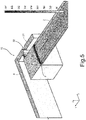
- shrinkage of the beams 20 generates forces (as indicated by the arrows A in Figures 4B and 5 ) that "pull" the second ends 2B, 3B of the driving arms 2, 3 towards the respective first ends 2A, 3A and cause rotation of the second ends 2B, 3B in opposite directions (as represented in Figure 4B with dashed lines and indicated by the arrows B).
- Rotation of the second ends 2B, 3B of the driving arms 2, 3 causes a corresponding rotation of the articulated arms 4, 5, which also rotate in the plane XY, amplifying the movement and bringing the gripping portions 6, 7 closer to each other ( Figure 4B , arrows C).
- Figure 5 shows in shades of grey the distribution of the stresses.
- the stresses are concentrated in the areas of the hinges 25, 26 and in the area of the beam 20 where this is connected to the second pillar 24 (indicated by the arrow F), areas that thus undergo deformation, as explained above.
- the gripping portions 6, 7 can then grip possible objects, materials, and structures in the space between them, at rest, and keep them in a fixed position during subsequent activities (e.g., of analysis) or displace them into other spatial positions when the manipulation device 1 is associated to, or comprises a spatial-displacement mechanism.
- the beams 20 and the piezoelectric strips 29 may be manufactured in a way similar to what described in the above patents (Italian patent application No. 102016000132144 , European patent application No. 17177446.6 , and U.S. patent application No. 15/638195 ), according to Figures 6A and 6B .
- the manipulation structure 50 is formed in a monolithic body 51 comprising basically a structural layer 200, a supporting layer 180 and a thin-film piezoelectric layer 191; the articulated arms 4, 5, the gripping portions 6, 7 and the articulation structures 10, 11 are formed by portions of the structural layer 200, in case overlaid by portions of the supporting layer 180; the beams 20 are formed by the supporting layer 180 carrying the thin-film piezoelectric layer 191 and the structural layer 200 is removed, except for at the ends (where are the pillars 23, 24).
- the pillars 23, 24, the articulated arms 4, 5, the gripping portions 6, 7 and the articulation structures 10, 11 have thus, in a first approximation, the same thickness (in the direction Z).
- each beam 20 is formed by the supporting layer 180, of semiconductor material such as epitaxially grown silicon, coated on the bottom by a bottom insulating layer 181 and on the top by a top insulating layer 182, for example, both of thermally grown silicon oxide.
- semiconductor material such as epitaxially grown silicon
- a stack extends over the top insulating layer 182 and is formed by a bottom electrode 183, of electrically conductive material, for example, titanium (Ti) or platinum (Pt); the thin-film piezoelectric layer 191; a top electrode 184, for example, of TiW; a first and a second dielectric layers 185, 186, for example of silicon oxide and silicon nitride deposited by CVD (Chemical Vapour Deposition); a contact line 189 of conductive material, for example aluminium and/or copper; and a passivation layer 190, for example of silicon oxide and/or silicon nitride deposited by CVD.
- a bottom electrode 183 of electrically conductive material, for example, titanium (Ti) or platinum (Pt); the thin-film piezoelectric layer 191; a top electrode 184, for example, of TiW; a first and a second dielectric layers 185, 186, for example of silicon oxide and silicon nitride deposited by CVD (Chem
- Each beam 20 has a first end 20A and a second end 20B, corresponding, respectively, to the first ends 2A, 3A of the driving arms 2, 3 and to the second ends 2B, 3B of the driving arms 2, 3 and fixed with respect to the pillars 23, 24.
- the first and second pillars 23, 24 have the same height and comprise respective portions 192 of the structural layer 200, preferably of semiconductor material such as silicon, overlaid by respective portions of the bottom insulating layer 181, the supporting layer 180, and the top insulating layer 182.
- the first pillar 23 may have a wide area, with portions (not illustrated) for the pads (contact pads) and possible other structures necessary for electrical connections with the electrodes 183, 184, as clear to the person skilled in the art.
- the articulated arms 4, 5 (the cross-section whereof is visible), the articulation structures 10, 11 (only part of a constraint arm 31 whereof is illustrated with dashed line) and the gripping portions 6, 7 (not visible in figure 6A ) are formed by the portions 192 of the structural layer 200 that also forms the pillars 23, 24, possibly overlaid by respective portions of the bottom insulating layer 181, the supporting layer 180, and the top insulating layer 182; thereby they have the same thickness (in the direction Z) as the pillars 23, 24.
- the substrate 28 may be formed in a separate semiconductor body, for example obtained from a first wafer that is worked separately from a second wafer forming the monolithic body 51 and integrating the driving arms 2, 3, the articulated arms 4, 5, the gripping portions 6, 7 and the articulation structures 10, 11, and subsequently bonded.
- the second wafer may be a SOI (Silicon-On-Insulator) type, wherein the intermediate oxide layer is intended to form the bottom insulating layer 181 of Figure 6B , one of the two silicon layers (e.g., the top one) is intended to form the supporting layer 180 of Figure 6A , and the other silicon layer (in the example, the bottom one) is intended to form the portions 192 of the structural layer 200 of Figure 6A .
- SOI Silicon-On-Insulator
- the second wafer is processed by thermally growing the top insulating layer 182 on the top silicon layer (supporting layer 180); depositing and patterning the layers to form the piezoelectric strips 29 and the corresponding biasing and electrical-connection structures, as well as the dielectric layers (forming regions 183, 184, 185, 186, 190 and 191 of Figure 6B ), in a per se known manner; lapping the back of the second wafer until the desired thickness for the pillars 23, 24, the hinge structures 32, the articulated arms 4, 5, and the gripping portions 6, 7, in the bottom silicon layer (structural layer 200); masking and etching the bottom silicon layer from the back to define the structure of the beams 20 from below, until reaching the bottom insulating layer 181 of Figure 6A (in practice, forming openings that have the shape, in plan view, of the beams 20).
- the first wafer is worked for selectively removing silicon. Then the first and second wafers are bonded together.
- the first pillar 23 comprises a first and a second silicon portions 192', 193, bonded together, and the second pillar 24 is formed by a single silicon portion 192", formed simultaneously with and with the same thickness as the first silicon portion 192' of the first pillar 23 in the structural layer 200.
- the structure of Figure 6B may be obtained, for example, by bonding two separately processed wafers.
- a sacrificial layer is grown on the substrate 28.
- the sacrificial layer is selectively removed to define through openings where the first pillars 23 and the constraint arms 31 are to be grown.
- An epitaxial polysilicon layer is grown on the sacrificial layer and in the openings.
- the epitaxial polysilicon layer is removed by lapping on the sacrificial layer and remains only in the through openings, thus forming the second portion 193 of the first pillars 23 (and of the constraint arms 31).
- the second wafer is processed in the same way as described above to etch the back of the beams 20 and form the piezoelectric strips 29, the respective electrical-connection structures and parts of the portions 192' and 192" of the structural layer 200. Then, the two wafers are bonded, aligning the portions 193 of the first wafer with the corresponding portions 192' and 192" (not yet completely defined) in the bottom silicon layer of the second wafer.
- Figures 1-5 is defined by etching the top silicon layer (supporting layer 180) as far as the bottom insulating layer 181, and the bottom insulating layer 181 and then the sacrificial oxide layer of the first wafer are removed to release the entire monolithic structure except for the first pillars 23 and the constraint arms 31 that remain fixed with respect to the substrate 28.
- the substrate 28 is selectively removed via partial sawing or via back etching using a dedicated mask.
- the supporting layer 180 forms both the driving arms 2, 3 and, on the ends 2A, 2B, 3A, 3B thereof, it extends on the portion s 192, 192', 192" of the structural layer 200; moreover, the piezoelectric strips 29 are formed as thin films on supporting layer 180 where the latter forms the beam 20.
- the supporting layer 180 and the insulating layers 181, 182 extend also on the articulation structures 10, 11, on the articulated arms 4, 5 and on the gripping elements 6, 7.
- the described manipulation device 1 has numerous advantages. It enables simple and accurate manipulation of objects and structures of very small dimensions, by virtue of the in-plane movement of its gripping portions 6, 7. In particular, it enables accurate control of the applied force and the position of the gripping portions 6, 7.
- the described manipulation device may be manufactured easily and at a low cost by using MEMS manufacturing techniques that enable an excellent precision and repeatability of the structure.
- the present manipulation device may be used also in humid environments or immersed in liquids, without any need to provide particularly long movement arms. This further increases the precision of movement and gripping.
- Figure 7 shows an embodiment of the first articulation structure 10, wherein the constraint arm 31 is arranged within the quadrilateral formed by the driving arms 2, 3 and the articulated arms 4, 5 (whereof only part of the first arm 2 and part of the first articulated arm 5 are visible).
- the end 2A of the first driving arm 2 turns according to arrow B
- the first articulated arm 4 turns according to arrow D, both in a counterclockwise direction (opposite to that of Figures 1-5 ).
- the second articulation structure 11 (not shown) is built in a similar way and arranged symmetrically with respect to an axis at 45° with respect to axes X and Y.
- the gripping portions 6, 7 are thus here in a normally closed position and are driven to open.
- the manipulation device of Figure 7 operates as a divaricator.
- Figure 8 shows another embodiment of the articulation structures 10, 11.
- the constraint arm 31 is aligned with the first articulated arm 4 and perpendicular to the first driving arm 2; no angled stretch is present here either.
- the first hinge 25 is arranged longitudinally with respect to the first driving arm 2, from the front face of the second end 2B, facing the first articulated arm 4, and the second hinge 26 is formed by a reduced width portion arranged between the constraint arm 31 and the first articulated arm 4 and aligned with both.
- the piezoelectric strip 29 when the piezoelectric strip 29 is biased, the first end 4A of the first articulated arm 4 turns according to the arrow C, in a counterclockwise direction.
- Figure 9 shows a different manipulation device, wherein the articulation structures 10, 11 are arranged asymmetrically.
- the first articulation structure 10, coupled to the first driving arm 2 and to the first articulated arm 4 is formed as in Figures 1-5 , with the constraint structure 10 laterally arranged with respect to the first driving arm 2.
- the second articulation structure 11, coupled to the second driving arm 3 and to the second articulated arm 5, is formed as described for Figure 8 (for the first articulation structure 10), with the constraint structure 11 coupled to the front face of the first driving arm 3.
- the gripping portions 6, 7 turn in an opposite direction, moving towards each other.
- FIG 10 shows an embodiment of the manipulation device wherein the driving arms 2, 3 are independently actuated.
- each driving arm 2, 3 is divided into a first part 102, respectively 103, and a second part 202, respectively 203, aligned to each other.
- the first parts 102, 103 extend between the respective first ends 2A, 3A, which are constrained to the substrate 28 (represented only schematically), and a common central area 80 that is cross-shaped, and the two second parts 202, 203 extend between the common central area 80 and the respective second ends 2B, 3B.
- Separate piezoelectric strips 129 extend on the first and second parts 102, 202, 103, 203 of the driving arms 2, 3, and can be driven independently. In this way, it is possible to drive just one of the manipulation arms 40, 41 and/or just one portion thereof, thus modulating the movement of the gripping portions 6, 7 and/or the force applied thereby.
- Figure 11 shows an embodiment of a manipulation device wherein the articulated arms 4, 5 are not rectilinear, but have the shape of broken lines, preferably arranged symmetrically respect to an axis arranged at 45° with respect to axes X and Y of the Cartesian system XYZ.
- the driving arms 2, 3 are arranged to form an L and have a first common end 150, constrained to the substrate 28 through just one first pillar 23 (represented only schematically).
- the driving arms 2, 3 may not have a first common end 150, but separate first ends 2A, 3A, each fixed with respect to a respective first pillar 23.
- the driving arms 2, 3 may be actuated independently, since they have separate piezoelectric strips 129.
- This solution allows the shape of the articulated arms 4, 5 to be adapted to the envisaged application, for example, to reduce the overall dimensions so as to avoid obstacles in the movement area of the articulated arms 4, 5 or just to meet particular spatial arrangement needs.
- the first and second driving arms 2, 3 have a first common end 150, as in Figure 11 , and extend (at rest) with an angle of less than 90°, for example, 45°.
- the articulated arms 4, 5 are not rectilinear, but each is formed by two non-aligned stretches, scissor-like, and the driving arms 2, 3 may be independently driven.
- the articulated arms 4, 5 are formed by a first and a second portions 250, 260.
- the first portions 250 of the articulated arms 4, 5 are articulated to the driving arms 2, 3, respectively, via the hinges 10, 11, respectively, and are substantially perpendicular to the driving arms.
- the second portions 260 of the articulated arms 4, 5 are inclined with respect to the first portions 250.
- the driving arms 2, 3 may have a first common end 150, as represented, or respective separate first ends 2A, 3A, constrained to the substrate 28 through respective first pillars 23, in a way not shown.
- the angle between the driving arms 2, 3, and the shape of the articulated arms 4, 5 may be modified according to the envisaged application so as to optimise the occupied space and the movement of the articulated arms, as well as of the gripping portions 6, 7, according to the needs.
- the manipulation device of Figure 13 is similar to the device of Figure 12 , except for that the second portions 260 of the articulated arms 4, 5 extend substantially parallel to each other and end with grippers 270 directed to each other, for holding very small objects and structures.
- the manipulation device of Figure 14 has a single driving arm 302 for both the articulated arms 4, 5.
- the driving arm 302 is formed by two portions 330, 340 T-like arranged, a first portion 330 whereof being constrained to the substrate 28 and a second portion 340 whereof being articulated to the articulated arms 2, 3.
- the first portion 330 is beam-like shaped and has a first and a second ends 330A, 330B.
- the first end 330A of the first portion 330 of the driving arm 302 is constrained to the substrate 28 through a first pillar 23, as illustrated in Figure 6A , and the second end 330B is fixed with respect to a central area of the second portion 340, which thus extends transverse to the first portion 330.
- a piezoelectric strip 29 extends on the first portion 330 of the driving arm 302.
- the second portion 340 of the driving arm 302 has the same thickness as the pillars 23, 24, so as to be rigid, and has two ends 340A, 340B articulated to the articulated arms 4, 5.
- the ends 340A, 340B of the second portion 340 of the driving arm 302 are shaped substantially like the second end 2B of the driving arm 2 of Figures 1-5 , are thus fixed with respect to respective second columns 24 (indicated with a dashed line) and are coupled to the articulated arms 4, 5 through the hinges 10 and 11, respectively.
- the manipulation device of Figure 15 has just one mobile arm 401, formed by a driving arm 402 and an articulated arm 403, for example, shaped like the first driving arm 2 and the first articulated arm 4 of Figures 1-5 and coupled through a constraint structure 404 similar to the articulation structure 11.
- the manipulation device of Figure 15 has a fixed counter-arm 405.
- the counter-arm 405 may comprise a first portion 406 and a second portion 407, formed as suspended beams and arranged at 90° with respect to each other so as to form approximately a quadrilateral with the mobile arm 401.
- the first portion 406 is here fixed with respect to the substrate 28 via a pillar (not illustrated), similar to the first pillar 23 of Figure 6 and arranged at one end 406A of the first portion 406 of the counter-arm 405; the rest of the counter-arm 405 may be completely suspended or be constrained to the substrate 28 via further pillars.
- the articulated arm 403 and the second portion 407 of the mobile arm 401 end with gripping ends 6, 7 similar to those represented Figures 1-5 .
- the manipulation device of Figure 16 operates as divaricator.
- the articulation structures 10 and 11 are formed as shown in Figure 7 .
- the driving arms 2, 3 have separate piezoelectric strips 129 and can thus be actuated independently.
- gripping elements 6, 7 may be arranged at intermediate positions of the articulated arms 4, 5 or a number of gripping elements could be arranged along one of the articulated arms, as, for example, in the embodiment of Figure 15 , if so desired in the envisaged application.
Landscapes
- Engineering & Computer Science (AREA)
- Robotics (AREA)
- Mechanical Engineering (AREA)
- Computer Hardware Design (AREA)
- Microelectronics & Electronic Packaging (AREA)
- Health & Medical Sciences (AREA)
- General Health & Medical Sciences (AREA)
- Toxicology (AREA)
- Chemical & Material Sciences (AREA)
- Analytical Chemistry (AREA)
- Manipulator (AREA)
- Micromachines (AREA)
Abstract
Description
- The present invention relates to a micro-electromechanical manipulation device with piezoelectric driving, and movable in the plane.
- Micromanipulation devices are known. They can operate in either contact or contactless mode and are based upon various physical principles, for example, of an optical type, an electrostatic type, a fluidostatic type (based upon Bernoulli's theorem), an ultrasound type, and/or a magnetic type. Each solution has characteristics that enable advantageous use thereof in particular conditions, but not in other conditions. However, none of them is completely satisfactory as regards the capacity of handling very small objects, of the order of microns, of various dimensions, in a simple way, with high precision, and at a low cost. This is desirable, for example, in applications of microelectronic type, in the fields of materials science, biology, and engineering of tissues (e.g., in micromanipulation of molecules, human tissue, and biological parts).
- On the other hand, the tendency towards miniaturization of products, such as micro-electromechanical systems (MEMS) that can be obtained with semiconductor technology, has stimulated an extensive research into techniques of micromanipulation and assembly. In particular, the development of miniaturised systems for handling and assembling micro-objects has become a major challenge for future precision engineering.
- Micromanipulators using MEMS technology based upon an electrostatic-actuation principle have thus been proposed. However, even micromanipulators of MEMS type do not completely meet the requirements existing in certain applications. In fact, the electrostatic force that can be obtained with these devices is rather weak. Consequently, to obtain sufficient gripping forces, known micromanipulators are supplied at high d.c. voltages, of the order of 100-200 V, which cannot be easily achieved and are in any case far higher than the values normally used in integrated circuits.
- Moreover, the proposed MEMS micromanipulators are not easy to use for manipulating objects and/or particles immersed in a liquid. In fact, in this type of devices, it is not simple to form electrically insulating layers that completely surround the arms of the manipulator; thus the risk of electrical discharges exists. To reduce this problem, the arms of the manipulator are frequently designed to have a considerable length in order to allow electrical insulation of the portion controlling the movement with respect to the gripping ends of the arms. This solution, however, reduces the gripping precision, in addition to increasing the overall dimensions of the device, and does not in any case always ensure electrical insulation.
-
DE 195 23 229 discloses a micromanipulator that is not integrated, having a piezotranslator forming a monomorph actuator that varies in length when electrically biased and is glued head-by-head to the gripping structure of semiconductor material. -
DE 101 07 402 discloses an improvement ofDE 195 23 229 able to grip round objects. -
JP H8 90478 CN 104 7647 347 - Italian patent application No.
102016000132144 filed on December 29, 2016 17177446 6 U.S. patent application No. 15/638 195 ) describes a micro-actuator of piezoelectric type formed by a beam element of semiconductor material and by a piezoelectric region extending thereon. One end of the beam element is fixed, and the other end is connected to a hinge element of a constraint structure that is non-deformable in the thickness direction of the beam. As explained in detail in this patent application, since the constraint structure is non-deformable in the thickness direction and by virtue of the hinge element, application of a voltage to the piezoelectric region causes a deformation of the beam element practically only in its extension plane. - The micro-actuator described in the above patent application is very advantageous in so far as it may be manufactured using conventional semiconductor micromanufacturing techniques, thus at reduced costs, in a highly controllable and reliable way.
- It is thus desirable to apply a similar operating principle to a micro-manipulator of the type considered herein.
- The aim of the present invention is to provide a micro-manipulator that may be manufactured using MEMS technology and based upon a piezoelectric operating principle, that is thus inexpensive, reliable, easy to control, and affords considerable freedom of design to the person skilled in the art.
- According to the present invention a manipulation device of a MEMS type is provided, as defined in the attached claims.
- For a better understanding of the present invention, preferred embodiments thereof are now described, purely by way of non-limiting example, with reference to the attached drawings, wherein:
-
Figure 1 is a perspective top view of an embodiment of the present manipulation device; -
Figure 2 is a perspective bottom view of the manipulation device ofFigure 1 ; -
Figure 3 is a top plan view of a detail of the manipulation device ofFigure 1 ; -
Figures 4A and 4B are top plan views, partially interrupted, of the manipulation device ofFigure 1 in a non-stressed position and in a stressed position, respectively; -
Figure 5 is a simulation of the stresses in a portion of the manipulation device ofFigure 1 ;
Figure 6A is a cross-section taken along plane VI-VI ofFigure 1 ; -
Figure 6B shows a variant ofFigure 6A ; -
Figures 7 and 8 are top plan views of variants of a detail of the present manipulation device; and -
Figures 9-16 are top plan views of different embodiments of the present manipulation device. -
Figures 1-4 show an embodiment of amanipulation device 1 manufactured using MEMS technology. - In detail, with reference to
Figure 1 ,manipulation device 1 comprises amanipulation structure 50, which is monolithic, and asubstrate 28, carrying themanipulation structure 50. Themanipulation structure 50 is formed by a first and asecond manipulation arms manipulation arms arms arms arms arms respective gripping portion first driving arm 2 has afirst end 2A constrained to thesubstrate 28, asecond end 2B articulated to afirst end 4A of the first articulatedarm 4, and thesecond driving arm 3 has afirst end 3A constrained to thesubstrate 28, asecond end 3B articulated to afirst end 5A of the second articulatedarm 5. The articulatedarms second ends 4B, respectively 5B, that are widened and form therespective gripping portion - At rest (in the absence of biasing), the gripping
portions manipulation device 1 without stresses, thus in a non-deformed condition, unless otherwise specified. - In the
manipulation device 1 ofFigures 1 and2 , the drivingarms arms arms arms 2, 3 (close to thesecond ends arms Figures 9-15 . -
Articulation structures second end driving arm first end arms arms arms arms gripping portions articulation structures substrate 28 are formed in a single semiconductor body (i.e., they are monolithic), as explained hereinafter with reference toFigures 6A and 6B . - In detail, each
driving arm Figures 6A, 6B ), fixed with respect to a first and to asecond pillars - Each
driving arm first driving arm 2 and X for the second driving arm 3) of the Cartesian reference system XYZ, even though the longitudinal directions of thedriving arms Figures 11-13 . - The
first ends arms substrate 28 by the respective first pillars 23 (see alsoFigures 6A and 6B ). Thefirst pillars 23 extend in a transverse direction to therespective driving arm first ends driving arms substrate 28, and are fixed with respect to them. - Each
second pillar 24 extends from thesecond end arms substrate 28 and is thus mobile with respect to the latter. Here, thesecond pillars 24 have a height (in direction Z) that is the same as thefirst pillars 23, and the substrate 28 (for example, of monocrystalline silicon) is removed underneath thesecond pillars 24, the articulatedarms gripping portions - For instance, the driving
arms pillars - A
piezoelectric strip 29 extends over thebeams 20, is for example, of PZT (Pb, Zr, TiO3), and has a thickness, for example, of 0.2-4 µm. Thepiezoelectric strip 29 covers almost the entire top surface of thebeams 20 and thus is also cross-shaped, whose arms have an extension (width and length) slightly smaller than the width and length of thebeams 20. - Each
articulation structure constraint arm 31 and ahinge structure 32 formed by a and asecond hinges Figure 3 for thefirst articulation structure 10 interposed between thesecond end 3B of thefirst driving arm 2 and thefirst end 4A of the first articulatedarm 4. Thus, hereinafter only thefirst articulation structure 10 will be described in detail; thesecond articulation structure 11 is made in the same way, but (in top plan view) is mirrored with respect to an axis at 45° with respect to axes X and Y of the Cartesian system XYZ, as may be seen inFigures 1 and2 . - In detail, the
constraint arm 31 is formed by a vertical wall here extending parallel to the respective driving arm (parallel to plane YZ for the first driving arm 2), here on the side of thefirst driving arm 2 not facing thegripping portions 6, 7 (external to the quadrilateral formed by thedriving arms arms 4, 5). Theconstraint arm 31 is connected to anangled stretch 35 of the firstarticulated arm 4 through thesecond hinge 26; theconstraint arm 31 is moreover connected to thesecond end 2B of thefirst driving arm 2 through both of thehinges constraint arm 31 here has a much shorter length than thefirst driving arm 2 and is anchored to thesubstrate 28, here on part of its length (in a direction Y), e.g., approximately one half of the length, as illustrated inFigure 2 , where the base area of the anchored portion of theconstraint arms 31 is represented in grey. Theconstraint arm 31 has the same height as thepillars constraint arm 31 has a width smaller than that of thebeam 20, for example, of 10-50 µm. - In
Figures 1-5 , theconstraint arm 31 extends parallel and as a prolongation of theangled stretch 35 of the first articulatedarm 4. However, the arrangement referred to above of theconstraint arm 31, parallel to thefirst driving arm 2, is not essential, and theconstraint arm 31 could have any shape, even not an elongated one. - The
angled stretch 35 here extends perpendicular to the first articulatedarm 4 from thefirst end 4A of the latter and is connected to thesecond end 2B of thefirst driving arm 2 via thefirst hinge 25. - The hinges 25, 26 are formed by portions having a smaller width than the
first driving arm 2 and of theconstraint arm 31. In detail, thefirst hinge 25 extends between thesecond end 2B of thefirst driving arm 2 and theangled stretch 35 and thus represents a connection portion here extending perpendicular to thefirst driving arm 2, theangled stretch 35, and theconstraint arm 31. Thesecond hinge 26 extends between theangled stretch 35 and theconstraint arm 31 and thus represents a connection portion extending parallel to theangled stretch 35, theconstraint arm 31, and thefirst driving arm 2. - For instance, in their point of minimum width, the
hinges constraint structures - Both the
hinges second pillar 24, theconstraint arm 31, and theangled stretch 35 and are not constrained to thesubstrate 28. - With this structure, by virtue of the large thickness and small width of the
constraint arm 31 and the ofhinge structure 32, these are substantially rigid in a vertical direction (direction of axis Z), but are compliant in the extension plane XY of thebeams 20 so as to allow rotation of the articulatedarms gripping portions articulation structures - In particular, and as explained in detail in aforementioned Italian patent application No.
102016000132144 piezoelectric material 29 are not biased, themanipulation device 1 is in its rest configuration, illustrated inFigures 1-3 ,4A (and 4B with dashed line). When the strips ofpiezoelectric material 29 are biased by applying a voltage (e.g., 30-40 V), they shrink and cause rotation of the second ends 2B, 3B of the drivingarms arms first driving arm 2 and in a clockwise direction for the second driving arm 3 -Figures 4B and5 ). - In fact, the first ends 2A, 3A of the driving
arms substrate 28 through the first pillars 23 (and thus, to a first approximation, do not have any degree of freedom). Instead, the second ends 2B, 3B are constrained in a direction Z by the constraint arms 31 (and are thus not free to deflect in this direction), but can move in the plane XY by virtue of the presence of thehinge structures 32, which provide (to a first approximation) an (angular) degree of freedom in the plane XY. - In practice, shrinkage of the
beams 20 generates forces (as indicated by the arrows A inFigures 4B and5 ) that "pull" the second ends 2B, 3B of the drivingarms Figure 4B with dashed lines and indicated by the arrows B). Rotation of the second ends 2B, 3B of the drivingarms arms gripping portions Figure 4B , arrows C).Figure 5 shows in shades of grey the distribution of the stresses. As may be noted, the stresses are concentrated in the areas of thehinges beam 20 where this is connected to the second pillar 24 (indicated by the arrow F), areas that thus undergo deformation, as explained above. - The
gripping portions manipulation device 1 is associated to, or comprises a spatial-displacement mechanism. - The
beams 20 and thepiezoelectric strips 29 may be manufactured in a way similar to what described in the above patents (Italian patent application No.102016000132144 17177446.6 U.S. patent application No. 15/638195 ), according toFigures 6A and 6B . - In these figures, the
manipulation structure 50 is formed in amonolithic body 51 comprising basically astructural layer 200, a supportinglayer 180 and a thin-film piezoelectric layer 191; the articulatedarms portions articulation structures structural layer 200, in case overlaid by portions of the supportinglayer 180; thebeams 20 are formed by the supportinglayer 180 carrying the thin-film piezoelectric layer 191 and thestructural layer 200 is removed, except for at the ends (where are thepillars 23, 24). Thepillars arms portions articulation structures - In detail,
Figure 6A , eachbeam 20 is formed by the supportinglayer 180, of semiconductor material such as epitaxially grown silicon, coated on the bottom by a bottom insulatinglayer 181 and on the top by a top insulatinglayer 182, for example, both of thermally grown silicon oxide. A stack extends over the top insulatinglayer 182 and is formed by abottom electrode 183, of electrically conductive material, for example, titanium (Ti) or platinum (Pt); the thin-film piezoelectric layer 191; atop electrode 184, for example, of TiW; a first and a seconddielectric layers contact line 189 of conductive material, for example aluminium and/or copper; and apassivation layer 190, for example of silicon oxide and/or silicon nitride deposited by CVD. - Each
beam 20 has afirst end 20A and asecond end 20B, corresponding, respectively, to the first ends 2A, 3A of the drivingarms arms pillars - In the embodiment of
Figure 6A , the first andsecond pillars respective portions 192 of thestructural layer 200, preferably of semiconductor material such as silicon, overlaid by respective portions of the bottom insulatinglayer 181, the supportinglayer 180, and the top insulatinglayer 182. - The
first pillar 23 may have a wide area, with portions (not illustrated) for the pads (contact pads) and possible other structures necessary for electrical connections with theelectrodes - In this embodiment, the articulated
arms 4, 5 (the cross-section whereof is visible), thearticulation structures 10, 11 (only part of aconstraint arm 31 whereof is illustrated with dashed line) and thegripping portions 6, 7 (not visible infigure 6A ) are formed by theportions 192 of thestructural layer 200 that also forms thepillars layer 181, the supportinglayer 180, and the top insulatinglayer 182; thereby they have the same thickness (in the direction Z) as thepillars substrate 28 may be formed in a separate semiconductor body, for example obtained from a first wafer that is worked separately from a second wafer forming themonolithic body 51 and integrating the drivingarms arms portions articulation structures - For instance, the second wafer may be a SOI (Silicon-On-Insulator) type, wherein the intermediate oxide layer is intended to form the bottom insulating
layer 181 ofFigure 6B , one of the two silicon layers (e.g., the top one) is intended to form the supportinglayer 180 ofFigure 6A , and the other silicon layer (in the example, the bottom one) is intended to form theportions 192 of thestructural layer 200 ofFigure 6A . For instance, the second wafer is processed by thermally growing the top insulatinglayer 182 on the top silicon layer (supporting layer 180); depositing and patterning the layers to form thepiezoelectric strips 29 and the corresponding biasing and electrical-connection structures, as well as the dielectric layers (formingregions Figure 6B ), in a per se known manner; lapping the back of the second wafer until the desired thickness for thepillars hinge structures 32, the articulatedarms gripping portions beams 20 from below, until reaching the bottom insulatinglayer 181 ofFigure 6A (in practice, forming openings that have the shape, in plan view, of the beams 20). - Simultaneously, before, or after, the first wafer is worked for selectively removing silicon. Then the first and second wafers are bonded together.
- According to a different embodiment, illustrated in
Figure 6B , thefirst pillar 23 comprises a first and asecond silicon portions 192', 193, bonded together, and thesecond pillar 24 is formed by asingle silicon portion 192", formed simultaneously with and with the same thickness as the first silicon portion 192' of thefirst pillar 23 in thestructural layer 200. - The structure of
Figure 6B may be obtained, for example, by bonding two separately processed wafers. In this case, for example, a sacrificial layer is grown on thesubstrate 28. The sacrificial layer is selectively removed to define through openings where thefirst pillars 23 and theconstraint arms 31 are to be grown. An epitaxial polysilicon layer is grown on the sacrificial layer and in the openings. The epitaxial polysilicon layer is removed by lapping on the sacrificial layer and remains only in the through openings, thus forming thesecond portion 193 of the first pillars 23 (and of the constraint arms 31). - Simultaneously, before, or after, the second wafer is processed in the same way as described above to etch the back of the
beams 20 and form thepiezoelectric strips 29, the respective electrical-connection structures and parts of theportions 192' and 192" of thestructural layer 200. Then, the two wafers are bonded, aligning theportions 193 of the first wafer with the correspondingportions 192' and 192" (not yet completely defined) in the bottom silicon layer of the second wafer. Then the geometry ofFigures 1-5 is defined by etching the top silicon layer (supporting layer 180) as far as the bottom insulatinglayer 181, and the bottom insulatinglayer 181 and then the sacrificial oxide layer of the first wafer are removed to release the entire monolithic structure except for thefirst pillars 23 and theconstraint arms 31 that remain fixed with respect to thesubstrate 28. - Before or after bonding the two wafers, the
substrate 28 is selectively removed via partial sawing or via back etching using a dedicated mask. - In both cases, as indicated, the supporting
layer 180 forms both the drivingarms ends structural layer 200; moreover, thepiezoelectric strips 29 are formed as thin films on supportinglayer 180 where the latter forms thebeam 20. In the shown embodiments, the supportinglayer 180 and the insulatinglayers articulation structures arms gripping elements - The described
manipulation device 1 has numerous advantages. It enables simple and accurate manipulation of objects and structures of very small dimensions, by virtue of the in-plane movement of itsgripping portions gripping portions - The described manipulation device may be manufactured easily and at a low cost by using MEMS manufacturing techniques that enable an excellent precision and repeatability of the structure.
- Since the actuation structure with
piezoelectric strips 29 is protected, the present manipulation device may be used also in humid environments or immersed in liquids, without any need to provide particularly long movement arms. This further increases the precision of movement and gripping. -
Figure 7 shows an embodiment of thefirst articulation structure 10, wherein theconstraint arm 31 is arranged within the quadrilateral formed by the drivingarms arms 4, 5 (whereof only part of thefirst arm 2 and part of the first articulatedarm 5 are visible). In this case, no angled stretch is present and, when thepiezoelectric strip 29 is biased, theend 2A of thefirst driving arm 2 turns according to arrow B, and the first articulatedarm 4 turns according to arrow D, both in a counterclockwise direction (opposite to that ofFigures 1-5 ). The second articulation structure 11 (not shown) is built in a similar way and arranged symmetrically with respect to an axis at 45° with respect to axes X and Y. Thegripping portions Figure 7 operates as a divaricator. -
Figure 8 shows another embodiment of thearticulation structures first articulation structure 10, in this embodiment, theconstraint arm 31 is aligned with the first articulatedarm 4 and perpendicular to thefirst driving arm 2; no angled stretch is present here either. Thefirst hinge 25 is arranged longitudinally with respect to thefirst driving arm 2, from the front face of thesecond end 2B, facing the first articulatedarm 4, and thesecond hinge 26 is formed by a reduced width portion arranged between theconstraint arm 31 and the first articulatedarm 4 and aligned with both. In this embodiment, as for the embodiment ofFigures 1-5 , when thepiezoelectric strip 29 is biased, thefirst end 4A of the first articulatedarm 4 turns according to the arrow C, in a counterclockwise direction. -
Figure 9 shows a different manipulation device, wherein thearticulation structures first articulation structure 10, coupled to thefirst driving arm 2 and to the first articulatedarm 4, is formed as inFigures 1-5 , with theconstraint structure 10 laterally arranged with respect to thefirst driving arm 2. Thesecond articulation structure 11, coupled to thesecond driving arm 3 and to the second articulatedarm 5, is formed as described forFigure 8 (for the first articulation structure 10), with theconstraint structure 11 coupled to the front face of thefirst driving arm 3. Here, notwithstanding the asymmetry of thearticulation structures manipulation device 1 is actuated, the grippingportions -
Figure 10 shows an embodiment of the manipulation device wherein the drivingarms arm first part 102, respectively 103, and asecond part 202, respectively 203, aligned to each other. In detail, thefirst parts central area 80 that is cross-shaped, and the twosecond parts central area 80 and the respectivesecond ends piezoelectric strips 129 extend on the first andsecond parts arms manipulation arms gripping portions -
Figure 11 shows an embodiment of a manipulation device wherein the articulatedarms - Moreover, here the driving
arms common end 150, constrained to thesubstrate 28 through just one first pillar 23 (represented only schematically). As an alternative to what illustrated, the drivingarms common end 150, but separate first ends 2A, 3A, each fixed with respect to a respectivefirst pillar 23. - Also here, the driving
arms piezoelectric strips 129. - This solution allows the shape of the articulated
arms arms - In
Figure 12 , the first and second drivingarms common end 150, as inFigure 11 , and extend (at rest) with an angle of less than 90°, for example, 45°. Also here, the articulatedarms arms arms second portions first portions 250 of the articulatedarms arms hinges second portions 260 of the articulatedarms first portions 250. Moreover, the drivingarms common end 150, as represented, or respective separate first ends 2A, 3A, constrained to thesubstrate 28 through respectivefirst pillars 23, in a way not shown. - In this embodiment, the angle between the driving
arms arms gripping portions - The manipulation device of
Figure 13 is similar to the device ofFigure 12 , except for that thesecond portions 260 of the articulatedarms grippers 270 directed to each other, for holding very small objects and structures. - The manipulation device of
Figure 14 has asingle driving arm 302 for both the articulatedarms - In detail, in
Figure 14 the drivingarm 302 is formed by twoportions 330, 340 T-like arranged, afirst portion 330 whereof being constrained to thesubstrate 28 and asecond portion 340 whereof being articulated to the articulatedarms - In particular, the
first portion 330 is beam-like shaped and has a first and a second ends 330A, 330B. Thefirst end 330A of thefirst portion 330 of the drivingarm 302 is constrained to thesubstrate 28 through afirst pillar 23, as illustrated inFigure 6A , and thesecond end 330B is fixed with respect to a central area of thesecond portion 340, which thus extends transverse to thefirst portion 330. Apiezoelectric strip 29 extends on thefirst portion 330 of the drivingarm 302. - The
second portion 340 of the drivingarm 302 has the same thickness as thepillars ends arms second portion 340 of the drivingarm 302 are shaped substantially like thesecond end 2B of the drivingarm 2 ofFigures 1-5 , are thus fixed with respect to respective second columns 24 (indicated with a dashed line) and are coupled to the articulatedarms hinges - When the
piezoelectric strip 129 is biased and shrinks, thesecond end 330B of thefirst portion 330 of the drivingarm 302 and thesecond portion 340, fixed to each other, move in the direction of the arrows A3 because of thearticulation structures arms Figures 4A, 4B . - Also this solution provides considerable freedom in designing the shape of the articulated
arms - The manipulation device of
Figure 15 has just onemobile arm 401, formed by a drivingarm 402 and an articulatedarm 403, for example, shaped like thefirst driving arm 2 and the first articulatedarm 4 ofFigures 1-5 and coupled through aconstraint structure 404 similar to thearticulation structure 11. Moreover, the manipulation device ofFigure 15 has a fixedcounter-arm 405. For instance, the counter-arm 405 may comprise afirst portion 406 and asecond portion 407, formed as suspended beams and arranged at 90° with respect to each other so as to form approximately a quadrilateral with themobile arm 401. Thefirst portion 406 is here fixed with respect to thesubstrate 28 via a pillar (not illustrated), similar to thefirst pillar 23 ofFigure 6 and arranged at oneend 406A of thefirst portion 406 of the counter-arm 405; the rest of the counter-arm 405 may be completely suspended or be constrained to thesubstrate 28 via further pillars. The articulatedarm 403 and thesecond portion 407 of themobile arm 401 end withgripping ends Figures 1-5 . - The manipulation device of
Figure 16 operates as divaricator. In fact, thearticulation structures Figure 7 . Here the drivingarms piezoelectric strips 129 and can thus be actuated independently. - Finally, it is clear that modifications and variations may be made to the manipulation device described and illustrated herein, without thereby departing from the scope of the present invention, as defined in the attached claims. For instance, the different embodiments described may be combined so as to provide further solutions.
- In addition, the
gripping elements arms Figure 15 , if so desired in the envisaged application.
Claims (16)
- A MEMS manipulation device (1), comprising a substrate (28) and a manipulation structure (50) extending on the substrate and including a body (51) formed by a structural layer (200), a supporting layer (180) on the structural layer, and a thin film piezoelectric layer (191) on the supporting layer,
the manipulation structure (50) including:a first manipulation arm (40; 401);a first gripping element (6) carried by the first manipulation arm (40; 401);a second manipulation arm (41; 405); anda second gripping element (7) carried by the second manipulation arm (41; 405) and facing the first gripping element (6);wherein the first manipulation arm (40; 401) comprises a first driving arm (2; 302; 402) and a first articulated arm (4; 403) having respective first and second ends (2A, 3A; 2B, 3B), the first end (2A) of the first driving arm (2; 302; 402) being constrained to the substrate (28) and the second end (2B) of the first driving arm (2; 302; 402) being articulated to the first end (4A) of the first articulated arm (4; 403) through a first articulation structure (10),the first driving arm (2; 302; 402) comprises a first beam element (20) formed by the supporting layer (180) and a first piezoelectric region (29; 129), formed by the thin film piezoelectric layer (191) on or in the first beam element, the first beam element (20) having a main extension in an extension plane and a thickness in a thickness direction, perpendicular to the extension plane, the thickness being smaller than the main extension, the first and the second ends of the first driving arm (2; 302; 402) comprising portions of the supporting layer (180) and portions (192; 192', 192") of the structural layer (200), andthe first articulation structure (10) comprises a first constraint element (31) not deformable in the thickness direction, and a first hinge structure (32), interposed between the first driving arm (2; 302; 402), the first articulated arm (4; 403), and the first constraint element (31). - The device according to claim 1, wherein the first constraint element (31) and the first articulated arm (4; 403) are formed by the structural layer (200) and have a greater thickness than the first beam element (20).
- The device according to claim 1 or 2, wherein the first constraint element (31) comprises a wall adjacent to the first beam element (20) and anchored to the substrate (28) .
- The device according to any of the preceding claims, wherein the first hinge structure (32) comprises a first hinge element (25) arranged between the second end (2B) of the first driving arm (2; 302; 402) and the first end (4A) of the first articulated arm (4; 403) and a second hinge element (26) arranged between the first end (4A) of the first articulated arm (4; 403) and the first constraint element (31), the first and second hinge elements (25, 26) having respective thicknesses, in the thickness direction, greater than the thickness of the first beam element (20) and a width in the extension plane smaller than the width of the first driving arm (2; 302; 402) and the first articulated arm (4; 403) and being formed by the structural layer (200).
- The device according to any of the preceding claims, wherein the first articulation structure (10) is arranged on a first side of the first beam element (20), the first articulated arm (4; 403) extends transverse to the first driving arm (2; 402), the first gripping element (6) is arranged on a second side of the first beam element (20), and the first end (4A) of the first articulated arm (4; 403) has an angled portion (35) extending along the first side of the first beam element (20) and coupled to the first articulation structure (10).
- The device according to any of claims 1-4, wherein the first articulation structure (10) faces a front surface of the second end (2B) of the first driving arm (2; 302; 402), and the first articulated arm (4; 403) extends transversely to the first driving arm.
- The device according to any of claims 1-4, wherein the first articulation structure (10) is arranged on a side of the first beam element (20), and the first articulated arm (4; 403) extends transversely to the first driving arm (2; 402) from the second end (2B) of the first driving arm.
- The device according to any of the preceding claims, wherein the second gripping element (7) is constrained to the substrate (28) and faces the first gripping element (6).
- The device according to any of claims 1-7, wherein the second manipulation arm (41) comprises a second driving arm (3) and a second articulated arm (5) having respective first and second ends (3A, 3B, 5A, 5B), the first end (3A) of the second driving arm (3) being constrained to the substrate (28) and the second end (3B) of the second driving arm (3) being articulated to the first end (5A) of the second articulated arm (5) through a second articulation structure (11),
wherein the second driving arm (3) comprises a second beam element (20) formed by the supporting layer (180) and a second piezoelectric region (29; 129) formed by the thin film piezoelectric layer (191) on or in the second beam element, the first and second ends (3A, 3B) of the second driving arm (3) comprising portions of the supporting layer (180) and portions (192; 192', 192") of the structural layer (200), and
the second articulation structure (11) comprises a second constraint element (31), not deformable in the thickness direction, and a second hinge structure (32), interposed between the second driving arm (3), the second articulated arm (5), and the second constraint element (31) . - The device according to claim 9, wherein the first and second driving arms (2; 302; 402, 3) are arranged crosswise to each other, and the first and second piezoelectric regions (29) are electrically coupled.
- The device according to claim 9, wherein the first and second driving arms (2; 302; 402, 3) are arranged crosswise to each other, and the first and second piezoelectric regions (129) are electrically insulated.
- The device according to any of claims 9-11, wherein the first and second articulated arms (4, 5) are perpendicular to the respective first and second driving arms (2,3).
- The device according to any of claims 9-11, wherein the first and second articulated arms (4, 5) have the shape of a broken line.
- The device according to any of claims 9-13, wherein the first and second driving arms (2, 3) have a first common end (150) constrained to the substrate (28) through a single pillar element extending in the thickness direction.
- The device according to any of claims 1-7, wherein the first driving arm (302) is T-shaped and comprises a first portion (330) and a second portion (340), the first portion (330) of the first driving arm (302) being constrained to the substrate (28) at the first end (330A) of the first driving arm (302) and the second portion (340) of the first driving arm (302) extending transversely to the first portion (330) of the first driving arm and defining the second end and a third end of the first driving arm (302);
the second manipulation arm further comprising a second articulated arm (5) and a second articulation structure (11);
the second articulated arm (5) having a first end and a second end;
the second gripping element (7) being carried by the second end of the second articulated arm (5) and facing the first gripping element (6); and
the second articulation structure (11) comprising a second constraint element (31), not deformable in the thickness direction, and a second hinge structure (32), interposed between the third end of the first driving arm (302), the first end of the second articulated arm (5), and the second constraint element (31). - The device according to any of claims 9-15, wherein the first and the second articulated arm (4, 5) and the first and second constraint element (31) are formed monolithically and comprise the structural layer (200) and the supporting layer (180).
Applications Claiming Priority (1)
| Application Number | Priority Date | Filing Date | Title |
|---|---|---|---|
| IT201800002364A IT201800002364A1 (en) | 2018-02-02 | 2018-02-02 | MICRO-ELECTRO-MECHANICAL MICRO-MANIPULATOR DEVICE WITH PIEZOELECTRIC CONTROL, MOBILE IN THE HOB |
Publications (2)
| Publication Number | Publication Date |
|---|---|
| EP3533569A1 true EP3533569A1 (en) | 2019-09-04 |
| EP3533569B1 EP3533569B1 (en) | 2021-01-20 |
Family
ID=62002327
Family Applications (1)
| Application Number | Title | Priority Date | Filing Date |
|---|---|---|---|
| EP19154620.9A Active EP3533569B1 (en) | 2018-02-02 | 2019-01-30 | Micro-electro-mechanical micro-manipulation device with piezoelectric driving, movable in the plane |
Country Status (4)
| Country | Link |
|---|---|
| US (1) | US11123878B2 (en) |
| EP (1) | EP3533569B1 (en) |
| CN (2) | CN110127590B (en) |
| IT (1) | IT201800002364A1 (en) |
Families Citing this family (5)
| Publication number | Priority date | Publication date | Assignee | Title |
|---|---|---|---|---|
| IT201600132144A1 (en) | 2016-12-29 | 2018-06-29 | St Microelectronics Srl | MICRO-ELECTRO-MECHANICAL ACTUATOR DEVICE WITH PIEZOELECTRIC CONTROL, MOBILE IN THE PLAN |
| IT201800002364A1 (en) * | 2018-02-02 | 2019-08-02 | St Microelectronics Srl | MICRO-ELECTRO-MECHANICAL MICRO-MANIPULATOR DEVICE WITH PIEZOELECTRIC CONTROL, MOBILE IN THE HOB |
| US11696507B2 (en) | 2018-12-14 | 2023-07-04 | Stmicroelectronics S.R.L. | Piezoelectric MEMS device with a suspended membrane having high mechanical shock resistance and manufacturing process thereof |
| US20230041174A1 (en) * | 2021-08-08 | 2023-02-09 | ViaMEMS Technologies, Inc. | Electrostatic devices to influence beams of charged particles |
| WO2025053179A1 (en) * | 2023-09-08 | 2025-03-13 | 国立大学法人九州大学 | Manipulator |
Citations (6)
| Publication number | Priority date | Publication date | Assignee | Title |
|---|---|---|---|---|
| JPH0890478A (en) | 1994-09-29 | 1996-04-09 | Shimadzu Corp | Micro grip |
| DE19523229A1 (en) | 1995-06-27 | 1997-01-02 | Riad Dipl Ing Salim | Micro-gripper for micro-assembly with substrate and microstructure body |
| DE10107402A1 (en) | 2001-02-14 | 2002-08-29 | Ruben Keoschkerjan | Piezo-electric parallel micro-gripper e.g. for positioning objects in micro-optics and micro-electronics, uses two parallel guides with solid hinges and two lever drives fixed on base |
| WO2010094102A1 (en) * | 2009-02-17 | 2010-08-26 | Yu Sun | Device for grasping and active release of micro and nano objects |
| CN104647347A (en) | 2014-09-26 | 2015-05-27 | 浙江大学 | Flexible hinge amplification-based piezoelectric microgripper |
| CN105058366A (en) * | 2015-08-20 | 2015-11-18 | 宁波大学 | Four-degree-of freedom piezoelectric micro-clamp |
Family Cites Families (18)
| Publication number | Priority date | Publication date | Assignee | Title |
|---|---|---|---|---|
| US5046773A (en) * | 1990-01-02 | 1991-09-10 | Hewlett-Packard Company | Micro-gripper assembly |
| DE19916960C2 (en) * | 1999-04-15 | 2002-12-05 | Bosch Gmbh Robert | Micro tool and method for manipulating components with this micro tool |
| BRPI0416808A (en) | 2003-11-20 | 2007-01-09 | Viking Technologies Lc | integral heat compensation for electro-mechanical actuator |
| US7518287B2 (en) | 2004-06-07 | 2009-04-14 | Panasonic Corporation | Actuator fine motion mechanism including the actuator, and camera module including the fine motion mechanism |
| JP4529012B2 (en) * | 2004-07-16 | 2010-08-25 | アオイ電子株式会社 | Nano gripper device |
| US7431364B2 (en) * | 2004-09-01 | 2008-10-07 | National Koasiung University Of Applied Sciences | Microgripper device for a micro-mechanism |
| CA2551191C (en) * | 2006-06-23 | 2016-04-05 | Keekyoung Kim | Electrothermally-driven mems microgrippers with integrated dual-axis capacitive force sensors |
| JP2008311521A (en) * | 2007-06-15 | 2008-12-25 | Aoi Electronics Co Ltd | Particle removal method, micro tweezers, atomic force microscope and charged particle beam device |
| KR101014226B1 (en) * | 2008-02-11 | 2011-02-14 | 전자부품연구원 | Gripper and its driving method |
| US8922094B2 (en) * | 2010-02-08 | 2014-12-30 | Uchicago Argonne, Llc | Microelectromechanical (MEMS) manipulators for control of nanoparticle coupling interactions |
| DE102010021867A1 (en) | 2010-05-28 | 2011-12-01 | Eurocopter Deutschland Gmbh | Power generator for attachment to a structure |
| FR2975935B1 (en) * | 2011-06-06 | 2013-07-05 | Centre Nat Rech Scient | TOOL FOR MICROTECHNIC CLIP |
| JP5916577B2 (en) | 2012-09-26 | 2016-05-11 | 富士フイルム株式会社 | Mirror driving device and driving method thereof |
| FR3030474B1 (en) | 2014-12-23 | 2022-01-21 | Commissariat Energie Atomique | DEVICE FOR TRANSFORMING AN OFF-PLAN MOVEMENT INTO IN-PLAN MOVEMENT AND/OR VICE VERSA |
| CN106092387B (en) * | 2015-04-30 | 2019-11-22 | 意法半导体股份有限公司 | Integrated piezoelectric sensor for detecting in-plane forces such as shock, acceleration, rotational force, etc. |
| US10062832B2 (en) | 2015-11-30 | 2018-08-28 | Sabic Global Technologies, B.V. | Methods and systems for making piezoelectric cantilever actuators |
| IT201600132144A1 (en) | 2016-12-29 | 2018-06-29 | St Microelectronics Srl | MICRO-ELECTRO-MECHANICAL ACTUATOR DEVICE WITH PIEZOELECTRIC CONTROL, MOBILE IN THE PLAN |
| IT201800002364A1 (en) * | 2018-02-02 | 2019-08-02 | St Microelectronics Srl | MICRO-ELECTRO-MECHANICAL MICRO-MANIPULATOR DEVICE WITH PIEZOELECTRIC CONTROL, MOBILE IN THE HOB |
-
2018
- 2018-02-02 IT IT201800002364A patent/IT201800002364A1/en unknown
-
2019
- 2019-01-30 EP EP19154620.9A patent/EP3533569B1/en active Active
- 2019-02-01 US US16/265,650 patent/US11123878B2/en active Active
- 2019-02-02 CN CN201910107464.5A patent/CN110127590B/en active Active
- 2019-02-02 CN CN201920186315.8U patent/CN210150712U/en not_active Withdrawn - After Issue
Patent Citations (6)
| Publication number | Priority date | Publication date | Assignee | Title |
|---|---|---|---|---|
| JPH0890478A (en) | 1994-09-29 | 1996-04-09 | Shimadzu Corp | Micro grip |
| DE19523229A1 (en) | 1995-06-27 | 1997-01-02 | Riad Dipl Ing Salim | Micro-gripper for micro-assembly with substrate and microstructure body |
| DE10107402A1 (en) | 2001-02-14 | 2002-08-29 | Ruben Keoschkerjan | Piezo-electric parallel micro-gripper e.g. for positioning objects in micro-optics and micro-electronics, uses two parallel guides with solid hinges and two lever drives fixed on base |
| WO2010094102A1 (en) * | 2009-02-17 | 2010-08-26 | Yu Sun | Device for grasping and active release of micro and nano objects |
| CN104647347A (en) | 2014-09-26 | 2015-05-27 | 浙江大学 | Flexible hinge amplification-based piezoelectric microgripper |
| CN105058366A (en) * | 2015-08-20 | 2015-11-18 | 宁波大学 | Four-degree-of freedom piezoelectric micro-clamp |
Also Published As
| Publication number | Publication date |
|---|---|
| US11123878B2 (en) | 2021-09-21 |
| US20190240844A1 (en) | 2019-08-08 |
| IT201800002364A1 (en) | 2019-08-02 |
| CN110127590B (en) | 2024-10-15 |
| CN210150712U (en) | 2020-03-17 |
| CN110127590A (en) | 2019-08-16 |
| EP3533569B1 (en) | 2021-01-20 |
Similar Documents
| Publication | Publication Date | Title |
|---|---|---|
| EP3533569B1 (en) | Micro-electro-mechanical micro-manipulation device with piezoelectric driving, movable in the plane | |
| US8724200B1 (en) | MEMS hierarchically-dimensioned optical mirrors and methods for manufacture thereof | |
| US7876026B2 (en) | Large force and displacement piezoelectric MEMS lateral actuation | |
| US6807332B1 (en) | Piezoelectric actuated optical switch | |
| EP1509802B1 (en) | Bulk silicon mirrors with hinges underneath | |
| EP1130442B1 (en) | Optical switches using dual axis micromirrors | |
| US6813412B2 (en) | Mems element having perpendicular portion formed from substrate | |
| US8139280B2 (en) | MEMS hierarchically-dimensioned deformable mirror | |
| US8691099B2 (en) | Process for fabricating MEMS devices | |
| US20040008400A1 (en) | Articulated MEMS electrostatic rotary actuator | |
| CN209890247U (en) | Piezoelectric micro-electromechanical actuator device and portable electronic device | |
| US20100007238A1 (en) | Method and structure for an out-of-plane compliant micro actuator | |
| US10770643B2 (en) | Piezoelectric micro-electro-mechanical actuator device, movable in the plane | |
| US6583031B2 (en) | Method of making a MEMS element having perpendicular portion formed from substrate | |
| JP3723431B2 (en) | Micro electromechanical optical device | |
| US6888979B2 (en) | MEMS mirrors with precision clamping mechanism | |
| US20040061414A1 (en) | Split spring for MEMS devices | |
| US6556741B1 (en) | MEMS optical switch with torsional hinge and method of fabrication thereof | |
| US20030168928A1 (en) | Parallel plate electrostatic actuation MEMS mirrors | |
| US7253550B2 (en) | Torsional electrostatic actuator | |
| US7453621B2 (en) | Micro mirrors with piezoelectric release mechanism | |
| US20040061924A1 (en) | Monolithic MEMS device for optical switches | |
| KR100400742B1 (en) | piezoelectric type micro mirror and method for fabricating the same | |
| US20040061923A1 (en) | Monolithic two-axis MEMS device for optical switches | |
| KR101041886B1 (en) | Corner cube retroreflector and its manufacturing method |
Legal Events
| Date | Code | Title | Description |
|---|---|---|---|
| PUAI | Public reference made under article 153(3) epc to a published international application that has entered the european phase |
Free format text: ORIGINAL CODE: 0009012 |
|
| STAA | Information on the status of an ep patent application or granted ep patent |
Free format text: STATUS: THE APPLICATION HAS BEEN PUBLISHED |
|
| AK | Designated contracting states |
Kind code of ref document: A1 Designated state(s): AL AT BE BG CH CY CZ DE DK EE ES FI FR GB GR HR HU IE IS IT LI LT LU LV MC MK MT NL NO PL PT RO RS SE SI SK SM TR |
|
| AX | Request for extension of the european patent |
Extension state: BA ME |
|
| STAA | Information on the status of an ep patent application or granted ep patent |
Free format text: STATUS: REQUEST FOR EXAMINATION WAS MADE |
|
| 17P | Request for examination filed |
Effective date: 20200206 |
|
| RBV | Designated contracting states (corrected) |
Designated state(s): AL AT BE BG CH CY CZ DE DK EE ES FI FR GB GR HR HU IE IS IT LI LT LU LV MC MK MT NL NO PL PT RO RS SE SI SK SM TR |
|
| RIC1 | Information provided on ipc code assigned before grant |
Ipc: B25J 9/00 20060101ALI20200622BHEP Ipc: B25J 15/08 20060101AFI20200622BHEP Ipc: B25J 7/00 20060101ALI20200622BHEP |
|
| GRAP | Despatch of communication of intention to grant a patent |
Free format text: ORIGINAL CODE: EPIDOSNIGR1 |
|
| STAA | Information on the status of an ep patent application or granted ep patent |
Free format text: STATUS: GRANT OF PATENT IS INTENDED |
|
| INTG | Intention to grant announced |
Effective date: 20200811 |
|
| GRAS | Grant fee paid |
Free format text: ORIGINAL CODE: EPIDOSNIGR3 |
|
| GRAA | (expected) grant |
Free format text: ORIGINAL CODE: 0009210 |
|
| STAA | Information on the status of an ep patent application or granted ep patent |
Free format text: STATUS: THE PATENT HAS BEEN GRANTED |
|
| AK | Designated contracting states |
Kind code of ref document: B1 Designated state(s): AL AT BE BG CH CY CZ DE DK EE ES FI FR GB GR HR HU IE IS IT LI LT LU LV MC MK MT NL NO PL PT RO RS SE SI SK SM TR |
|
| REG | Reference to a national code |
Ref country code: GB Ref legal event code: FG4D |
|
| REG | Reference to a national code |
Ref country code: CH Ref legal event code: EP |
|
| REG | Reference to a national code |
Ref country code: DE Ref legal event code: R096 Ref document number: 602019002207 Country of ref document: DE |
|
| REG | Reference to a national code |
Ref country code: AT Ref legal event code: REF Ref document number: 1355979 Country of ref document: AT Kind code of ref document: T Effective date: 20210215 |
|
| REG | Reference to a national code |
Ref country code: IE Ref legal event code: FG4D |
|
| REG | Reference to a national code |
Ref country code: NL Ref legal event code: MP Effective date: 20210120 |
|
| REG | Reference to a national code |
Ref country code: LT Ref legal event code: MG9D |
|
| REG | Reference to a national code |
Ref country code: AT Ref legal event code: MK05 Ref document number: 1355979 Country of ref document: AT Kind code of ref document: T Effective date: 20210120 |
|
| PG25 | Lapsed in a contracting state [announced via postgrant information from national office to epo] |
Ref country code: BG Free format text: LAPSE BECAUSE OF FAILURE TO SUBMIT A TRANSLATION OF THE DESCRIPTION OR TO PAY THE FEE WITHIN THE PRESCRIBED TIME-LIMIT Effective date: 20210420 Ref country code: FI Free format text: LAPSE BECAUSE OF FAILURE TO SUBMIT A TRANSLATION OF THE DESCRIPTION OR TO PAY THE FEE WITHIN THE PRESCRIBED TIME-LIMIT Effective date: 20210120 Ref country code: HR Free format text: LAPSE BECAUSE OF FAILURE TO SUBMIT A TRANSLATION OF THE DESCRIPTION OR TO PAY THE FEE WITHIN THE PRESCRIBED TIME-LIMIT Effective date: 20210120 Ref country code: GR Free format text: LAPSE BECAUSE OF FAILURE TO SUBMIT A TRANSLATION OF THE DESCRIPTION OR TO PAY THE FEE WITHIN THE PRESCRIBED TIME-LIMIT Effective date: 20210421 Ref country code: PT Free format text: LAPSE BECAUSE OF FAILURE TO SUBMIT A TRANSLATION OF THE DESCRIPTION OR TO PAY THE FEE WITHIN THE PRESCRIBED TIME-LIMIT Effective date: 20210520 Ref country code: NO Free format text: LAPSE BECAUSE OF FAILURE TO SUBMIT A TRANSLATION OF THE DESCRIPTION OR TO PAY THE FEE WITHIN THE PRESCRIBED TIME-LIMIT Effective date: 20210420 Ref country code: LT Free format text: LAPSE BECAUSE OF FAILURE TO SUBMIT A TRANSLATION OF THE DESCRIPTION OR TO PAY THE FEE WITHIN THE PRESCRIBED TIME-LIMIT Effective date: 20210120 |
|
| PG25 | Lapsed in a contracting state [announced via postgrant information from national office to epo] |
Ref country code: AT Free format text: LAPSE BECAUSE OF FAILURE TO SUBMIT A TRANSLATION OF THE DESCRIPTION OR TO PAY THE FEE WITHIN THE PRESCRIBED TIME-LIMIT Effective date: 20210120 Ref country code: RS Free format text: LAPSE BECAUSE OF FAILURE TO SUBMIT A TRANSLATION OF THE DESCRIPTION OR TO PAY THE FEE WITHIN THE PRESCRIBED TIME-LIMIT Effective date: 20210120 Ref country code: LV Free format text: LAPSE BECAUSE OF FAILURE TO SUBMIT A TRANSLATION OF THE DESCRIPTION OR TO PAY THE FEE WITHIN THE PRESCRIBED TIME-LIMIT Effective date: 20210120 Ref country code: PL Free format text: LAPSE BECAUSE OF FAILURE TO SUBMIT A TRANSLATION OF THE DESCRIPTION OR TO PAY THE FEE WITHIN THE PRESCRIBED TIME-LIMIT Effective date: 20210120 Ref country code: SE Free format text: LAPSE BECAUSE OF FAILURE TO SUBMIT A TRANSLATION OF THE DESCRIPTION OR TO PAY THE FEE WITHIN THE PRESCRIBED TIME-LIMIT Effective date: 20210120 |
|
| PG25 | Lapsed in a contracting state [announced via postgrant information from national office to epo] |
Ref country code: IS Free format text: LAPSE BECAUSE OF FAILURE TO SUBMIT A TRANSLATION OF THE DESCRIPTION OR TO PAY THE FEE WITHIN THE PRESCRIBED TIME-LIMIT Effective date: 20210520 Ref country code: LU Free format text: LAPSE BECAUSE OF NON-PAYMENT OF DUE FEES Effective date: 20210130 |
|
| REG | Reference to a national code |
Ref country code: BE Ref legal event code: MM Effective date: 20210131 |
|
| REG | Reference to a national code |
Ref country code: DE Ref legal event code: R097 Ref document number: 602019002207 Country of ref document: DE |
|
| PG25 | Lapsed in a contracting state [announced via postgrant information from national office to epo] |
Ref country code: MC Free format text: LAPSE BECAUSE OF FAILURE TO SUBMIT A TRANSLATION OF THE DESCRIPTION OR TO PAY THE FEE WITHIN THE PRESCRIBED TIME-LIMIT Effective date: 20210120 Ref country code: CZ Free format text: LAPSE BECAUSE OF FAILURE TO SUBMIT A TRANSLATION OF THE DESCRIPTION OR TO PAY THE FEE WITHIN THE PRESCRIBED TIME-LIMIT Effective date: 20210120 Ref country code: EE Free format text: LAPSE BECAUSE OF FAILURE TO SUBMIT A TRANSLATION OF THE DESCRIPTION OR TO PAY THE FEE WITHIN THE PRESCRIBED TIME-LIMIT Effective date: 20210120 Ref country code: SM Free format text: LAPSE BECAUSE OF FAILURE TO SUBMIT A TRANSLATION OF THE DESCRIPTION OR TO PAY THE FEE WITHIN THE PRESCRIBED TIME-LIMIT Effective date: 20210120 |
|
| PLBE | No opposition filed within time limit |
Free format text: ORIGINAL CODE: 0009261 |
|
| STAA | Information on the status of an ep patent application or granted ep patent |
Free format text: STATUS: NO OPPOSITION FILED WITHIN TIME LIMIT |
|
| PG25 | Lapsed in a contracting state [announced via postgrant information from national office to epo] |
Ref country code: RO Free format text: LAPSE BECAUSE OF FAILURE TO SUBMIT A TRANSLATION OF THE DESCRIPTION OR TO PAY THE FEE WITHIN THE PRESCRIBED TIME-LIMIT Effective date: 20210120 Ref country code: SK Free format text: LAPSE BECAUSE OF FAILURE TO SUBMIT A TRANSLATION OF THE DESCRIPTION OR TO PAY THE FEE WITHIN THE PRESCRIBED TIME-LIMIT Effective date: 20210120 Ref country code: DK Free format text: LAPSE BECAUSE OF FAILURE TO SUBMIT A TRANSLATION OF THE DESCRIPTION OR TO PAY THE FEE WITHIN THE PRESCRIBED TIME-LIMIT Effective date: 20210120 |
|
| 26N | No opposition filed |
Effective date: 20211021 |
|
| PG25 | Lapsed in a contracting state [announced via postgrant information from national office to epo] |
Ref country code: ES Free format text: LAPSE BECAUSE OF FAILURE TO SUBMIT A TRANSLATION OF THE DESCRIPTION OR TO PAY THE FEE WITHIN THE PRESCRIBED TIME-LIMIT Effective date: 20210120 Ref country code: FR Free format text: LAPSE BECAUSE OF NON-PAYMENT OF DUE FEES Effective date: 20210320 Ref country code: IE Free format text: LAPSE BECAUSE OF NON-PAYMENT OF DUE FEES Effective date: 20210130 Ref country code: AL Free format text: LAPSE BECAUSE OF FAILURE TO SUBMIT A TRANSLATION OF THE DESCRIPTION OR TO PAY THE FEE WITHIN THE PRESCRIBED TIME-LIMIT Effective date: 20210120 |
|
| PG25 | Lapsed in a contracting state [announced via postgrant information from national office to epo] |
Ref country code: SI Free format text: LAPSE BECAUSE OF FAILURE TO SUBMIT A TRANSLATION OF THE DESCRIPTION OR TO PAY THE FEE WITHIN THE PRESCRIBED TIME-LIMIT Effective date: 20210120 |
|
| PG25 | Lapsed in a contracting state [announced via postgrant information from national office to epo] |
Ref country code: IT Free format text: LAPSE BECAUSE OF FAILURE TO SUBMIT A TRANSLATION OF THE DESCRIPTION OR TO PAY THE FEE WITHIN THE PRESCRIBED TIME-LIMIT Effective date: 20210120 |
|
| PG25 | Lapsed in a contracting state [announced via postgrant information from national office to epo] |
Ref country code: IS Free format text: LAPSE BECAUSE OF FAILURE TO SUBMIT A TRANSLATION OF THE DESCRIPTION OR TO PAY THE FEE WITHIN THE PRESCRIBED TIME-LIMIT Effective date: 20210520 |
|
| PG25 | Lapsed in a contracting state [announced via postgrant information from national office to epo] |
Ref country code: BE Free format text: LAPSE BECAUSE OF NON-PAYMENT OF DUE FEES Effective date: 20210131 |
|
| REG | Reference to a national code |
Ref country code: CH Ref legal event code: PL |
|
| PG25 | Lapsed in a contracting state [announced via postgrant information from national office to epo] |
Ref country code: LI Free format text: LAPSE BECAUSE OF NON-PAYMENT OF DUE FEES Effective date: 20220131 Ref country code: CH Free format text: LAPSE BECAUSE OF NON-PAYMENT OF DUE FEES Effective date: 20220131 |
|
| PG25 | Lapsed in a contracting state [announced via postgrant information from national office to epo] |
Ref country code: NL Free format text: LAPSE BECAUSE OF NON-PAYMENT OF DUE FEES Effective date: 20210120 Ref country code: CY Free format text: LAPSE BECAUSE OF FAILURE TO SUBMIT A TRANSLATION OF THE DESCRIPTION OR TO PAY THE FEE WITHIN THE PRESCRIBED TIME-LIMIT Effective date: 20210120 |
|
| PG25 | Lapsed in a contracting state [announced via postgrant information from national office to epo] |
Ref country code: HU Free format text: LAPSE BECAUSE OF FAILURE TO SUBMIT A TRANSLATION OF THE DESCRIPTION OR TO PAY THE FEE WITHIN THE PRESCRIBED TIME-LIMIT; INVALID AB INITIO Effective date: 20190130 |
|
| GBPC | Gb: european patent ceased through non-payment of renewal fee |
Effective date: 20230130 |
|
| PG25 | Lapsed in a contracting state [announced via postgrant information from national office to epo] |
Ref country code: GB Free format text: LAPSE BECAUSE OF NON-PAYMENT OF DUE FEES Effective date: 20230130 |
|
| PG25 | Lapsed in a contracting state [announced via postgrant information from national office to epo] |
Ref country code: MK Free format text: LAPSE BECAUSE OF FAILURE TO SUBMIT A TRANSLATION OF THE DESCRIPTION OR TO PAY THE FEE WITHIN THE PRESCRIBED TIME-LIMIT Effective date: 20210120 |
|
| PG25 | Lapsed in a contracting state [announced via postgrant information from national office to epo] |
Ref country code: MT Free format text: LAPSE BECAUSE OF FAILURE TO SUBMIT A TRANSLATION OF THE DESCRIPTION OR TO PAY THE FEE WITHIN THE PRESCRIBED TIME-LIMIT Effective date: 20210120 |
|
| PG25 | Lapsed in a contracting state [announced via postgrant information from national office to epo] |
Ref country code: TR Free format text: LAPSE BECAUSE OF FAILURE TO SUBMIT A TRANSLATION OF THE DESCRIPTION OR TO PAY THE FEE WITHIN THE PRESCRIBED TIME-LIMIT Effective date: 20210120 |
|
| PGFP | Annual fee paid to national office [announced via postgrant information from national office to epo] |
Ref country code: DE Payment date: 20251217 Year of fee payment: 8 |