EP3532896B1 - Variable iris device with shape memory alloy element - Google Patents
Variable iris device with shape memory alloy element Download PDFInfo
- Publication number
- EP3532896B1 EP3532896B1 EP18834009.5A EP18834009A EP3532896B1 EP 3532896 B1 EP3532896 B1 EP 3532896B1 EP 18834009 A EP18834009 A EP 18834009A EP 3532896 B1 EP3532896 B1 EP 3532896B1
- Authority
- EP
- European Patent Office
- Prior art keywords
- aperture
- shuttering
- aperture device
- shape memory
- memory alloy
- Prior art date
- Legal status (The legal status is an assumption and is not a legal conclusion. Google has not performed a legal analysis and makes no representation as to the accuracy of the status listed.)
- Active
Links
Images




Classifications
-
- G—PHYSICS
- G03—PHOTOGRAPHY; CINEMATOGRAPHY; ANALOGOUS TECHNIQUES USING WAVES OTHER THAN OPTICAL WAVES; ELECTROGRAPHY; HOLOGRAPHY
- G03B—APPARATUS OR ARRANGEMENTS FOR TAKING PHOTOGRAPHS OR FOR PROJECTING OR VIEWING THEM; APPARATUS OR ARRANGEMENTS EMPLOYING ANALOGOUS TECHNIQUES USING WAVES OTHER THAN OPTICAL WAVES; ACCESSORIES THEREFOR
- G03B9/00—Exposure-making shutters; Diaphragms
- G03B9/08—Shutters
- G03B9/36—Sliding rigid plate
- G03B9/40—Double plate
-
- G—PHYSICS
- G03—PHOTOGRAPHY; CINEMATOGRAPHY; ANALOGOUS TECHNIQUES USING WAVES OTHER THAN OPTICAL WAVES; ELECTROGRAPHY; HOLOGRAPHY
- G03B—APPARATUS OR ARRANGEMENTS FOR TAKING PHOTOGRAPHS OR FOR PROJECTING OR VIEWING THEM; APPARATUS OR ARRANGEMENTS EMPLOYING ANALOGOUS TECHNIQUES USING WAVES OTHER THAN OPTICAL WAVES; ACCESSORIES THEREFOR
- G03B9/00—Exposure-making shutters; Diaphragms
- G03B9/08—Shutters
-
- G—PHYSICS
- G03—PHOTOGRAPHY; CINEMATOGRAPHY; ANALOGOUS TECHNIQUES USING WAVES OTHER THAN OPTICAL WAVES; ELECTROGRAPHY; HOLOGRAPHY
- G03B—APPARATUS OR ARRANGEMENTS FOR TAKING PHOTOGRAPHS OR FOR PROJECTING OR VIEWING THEM; APPARATUS OR ARRANGEMENTS EMPLOYING ANALOGOUS TECHNIQUES USING WAVES OTHER THAN OPTICAL WAVES; ACCESSORIES THEREFOR
- G03B9/00—Exposure-making shutters; Diaphragms
- G03B9/02—Diaphragms
-
- H—ELECTRICITY
- H04—ELECTRIC COMMUNICATION TECHNIQUE
- H04N—PICTORIAL COMMUNICATION, e.g. TELEVISION
- H04N23/00—Cameras or camera modules comprising electronic image sensors; Control thereof
- H04N23/50—Constructional details
- H04N23/55—Optical parts specially adapted for electronic image sensors; Mounting thereof
-
- H—ELECTRICITY
- H05—ELECTRIC TECHNIQUES NOT OTHERWISE PROVIDED FOR
- H05K—PRINTED CIRCUITS; CASINGS OR CONSTRUCTIONAL DETAILS OF ELECTRIC APPARATUS; MANUFACTURE OF ASSEMBLAGES OF ELECTRICAL COMPONENTS
- H05K3/00—Apparatus or processes for manufacturing printed circuits
- H05K3/36—Assembling printed circuits with other printed circuits
- H05K3/361—Assembling flexible printed circuits with other printed circuits
-
- G—PHYSICS
- G03—PHOTOGRAPHY; CINEMATOGRAPHY; ANALOGOUS TECHNIQUES USING WAVES OTHER THAN OPTICAL WAVES; ELECTROGRAPHY; HOLOGRAPHY
- G03B—APPARATUS OR ARRANGEMENTS FOR TAKING PHOTOGRAPHS OR FOR PROJECTING OR VIEWING THEM; APPARATUS OR ARRANGEMENTS EMPLOYING ANALOGOUS TECHNIQUES USING WAVES OTHER THAN OPTICAL WAVES; ACCESSORIES THEREFOR
- G03B2205/00—Adjustment of optical system relative to image or object surface other than for focusing
- G03B2205/0053—Driving means for the movement of one or more optical element
- G03B2205/0076—Driving means for the movement of one or more optical element using shape memory alloys
Definitions
- the present disclosure relates to optical shutters. More particularly, it relates to a variable iris device with shape memory alloy element.
- variable iris devices comprising shape memory alloy elements are known from WO2010/058947 A , US3883885 A , JP2005134438 A .
- an aperture device comprising: a first shuttering surface comprising a first opening and a first lateral slot; a second shuttering surface partially overlapping the first shuttering surface, the second shuttering surface comprising a second opening and a second lateral slot, the first and second opening forming an aperture; a lever comprising: a first pin inserted in the first lateral slot, a second pin inserted in the second lateral slot, a third pin configured to allow rotation of the lever between two end positions, a first end position corresponding to a fully opened state for the aperture, the second end position corresponding to an at least partially closed state for the aperture, a fourth pin having a reentrant slot; and a shape memory alloy wire slotted in the fourth pin.
- the present disclosure describes an aperture system which can control the size of an aperture window.
- the aperture system can control the degree of opening of the aperture window, between a fully closed position and a fully open position.
- the aperture system may control the aperture so that it is open only partially, and may therefore be referred to as a variable iris device.
- the aperture mechanism can be driven by a shape memory allow (SMA) wire and a torsion spring which can push against the SMA wire, generating a force.
- SMA shape memory allow
- a shape-memory alloy is an alloy that has a physical "memory" of its original shape. The SMA wire can therefore deform and return to its original shape.
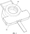
- Fig. 1 illustrates an exemplary front view of an aperture control device (105) integrated with a lens system (110).
- Fig. 2 illustrates an exemplary back view of an aperture control device (205) integrated with a lens system, for example a lens barrel (210).
- a lens system may comprise multiple lenses.
- Such lens system may be termed a lens barrel, and comprise different types of lenses.
- a shutter can be inserted between two adjacent lenses which are part of the lens barrel.
- the present disclosure describes an aperture system based on a shape memory alloy wire, which implements a shutter mechanism within a lens barrel.
- Fig. 3 illustrates an exemplary blowout view of an aperture device, comprising several components, and a lens barrel (305).
- the aperture mechanism may comprise: a cover (310) to protect the internal components from external damage; an SMA wire (315); two terminals or supporting elements (320), to which the SMA wire can be attached to for mechanical support and electrical connection.
- the SMA wire can actuate the two supporting elements (320) in order to actuate attached components, such as the shutter surfaces which can block light between lenses.
- a torsion spring (325) can provide an opposing force to the SMA wire in order to allow bidirectional control of the shutter, from closed to open and from open to closed.
- a lever element (330) moving between two positions can actuate on the shutter surfaces based on the SMA movement.
- the shutter surfaces can also be termed blades due to their flat shape.
- the shutter surfaces comprise a first flat element or shutter surface (335) and a second flat element or shutter surface (340).
- these shutter surfaces, window surfaces, or aperture surfaces can have an inner opening, for example shaped approximately like a teardrop, as visible in Fig. 3 .
- the shutter surfaces may also have a lateral portion forming a U shape.
- This U-shaped groove, or slot also shown in Fig. 3 , accommodates one end of the lever (330). In this way, each of the two ends of the lever (330) is inserted in the corresponding slot of each shutter surface (335).
- the lever, and in turn, the two shutter surfaces through the U-shaped slots move relative to each other.
- the amount of relative movement of the two blades (335) and (340) determines the degree of aperture of the shutter.
- the shutter may also comprise a base housing (345) to house the components listed above, and a flexible printed circuit (FPC) as illustrated in Fig. 3 (350).
- the FPC may be attached to the external surface of the housing (345) and provide electronic control of the shutter's operation, such as, for example, electric control of the SMA wire and window aperture.
- the user may operate a digital control on a camera, which in turn could electronically control the shutter through the FPC.
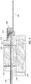
- Fig. 4 illustrates a cross-sectional lateral view of an exemplary aperture device.
- the shutter blades (420) are placed between adjacent lenses (425) and (430).
- the FPC (435) can transmit control signals to the SMA wire (415), which can in turn actuate the lever (410) slotted within the slots of the shutter surfaces (420).
- the lens elements (425, 430) can be housed within a lens barrel (440).
- the shutter surfaces (420) can be distinguished in Fig. 4 with reference to Fig. 3 .
- Blade (340) in Fig. 3 corresponds to (445) in Fig. 4
- blade (335) in Fig. 3 corresponds to (450) in Fig. 4 .
- an FPC comprises flexible electronics.
- Flexible electronics are electronic circuits assembled by mounting electronic devices on flexible plastic substrates, such as polyimide or transparent conductive polyester films.
- a flexible substrate may also be fabricated with other materials, such as, for example, polyether ether ketone (PEEK), a colorless organic thermoplastic polymer.
- Flex circuits can also comprise silver circuits screen printed on polyester.
- Flexible electronic assemblies may be manufactured using identical components used for rigid printed circuit boards, allowing the board to conform to a desired shape, or to flex during its use.
- An alternative approach to flexible electronics consists in various etching techniques to thin down a traditional silicon substrate to few tens of micrometers to gain reasonable flexibility. These processes are referred to as flexible silicon, and the flexible circuits made of silicon can have, for example, a bending radius of about 5 mm.
- the FPC can be made with a photolithographic technology.
- a possible process comprises laminating very thin (e.g. 0.07 mm) copper strips in between two layers of polyethylene terephthalate (PET). These PET layers, e.g. 0.05 mm thick, can be coated with a thermosetting adhesive which is activated during the lamination process.
- PET polyethylene terephthalate
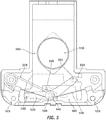
- Figs. 5 and 6 provide an internal view of the aperture mechanism in two different states of operation.
- the two shutter blades are aligned (505) so that the aperture is fully open (510).
- the SMA wire (520) is attached to the two supporting elements (515).
- the SMA wire can act on the lever (530) to actuate it between positions.
- the lever's two extremities can be slotted within the slots (535) of the shuttering blades.
- a torsion spring (525) provides a counteracting force to the SMA wire.
- the spring can facilitate the return of the lever in the previous position, depending on the state of the SMA wire.
- Fig. 6 shows a different state after the SMA wire has actuated the lever, which in turn actuates the shuttering blades.
- the two blades (605, 610) are aligned so that the aperture is closed, or partially closed (615).
- the mechanical elements are configured to be very thin in order to save space and fabricate a compact aperture mechanism.
- the aperture window size (created by the blade shutters) can be controlled by the SMA wire through an electrical resistance feedback control.
- the SMA wire electrical resistance changes when its physical dimensions are modified, such as through a change of its diameter and length. The diameter and length will change while the SMA is pushing on or being pushed by the lever. The lever, in turn, pushes or pulls on the shuttering blades. Therefore, by controlling the SMA wire resistance, it is possible to control the window aperture size.
- the aperture mechanism can be used as an iris for a mobile phone camera.
- Fig. 5 the two blades are hooked, through the respective slots, on the two pins (555, 560) at the extremities of the lever. Being moved by the lever, the two blades can have a symmetrical movement, which can be noted comparing Figs. 5 and 6 , as in one figure the blades' slots are up and down, and in the next figure are in the opposite, symmetrical position, down and up (620).
- the center aperture (510) of the two blades will create a window and control the light ray reaching the image sensor through the lenses.
- the lever can comprise a pin (540) to rotate on the base (565).
- the lever can also comprise another pin on the opposite side of the rotation pin (the opposite side of the lever's surfaces).
- the second pin can be off-centered relative to the first pin, and can be a hook pin (545).
- the hook pin can hook onto the SMA wire, and will be pushed by the SMA when the current is applied.
- the other side of the hook pin can hook onto one side of the torsion spring (550).
- the torsion spring is generating a force in the opposite direction of the force generated by the SMA wire.
- Fig. 7 illustrates a view of a lens assembly and lever.
- the lever can comprise two pins at the two opposite ends (710, 705) corresponding to (555, 560); a pin (715) corresponding to (540) to allow rotation on the base; and a hook pin (720) corresponding to (545) to hook onto the SMA wire.
- the lens barrel on the lens assembly can comprise a slot (725) to allow the iris device to be inserted partially within the lens assembly, as also illustrated in Figs. 1-2 .
- the SMA wire may have, in some embodiments, a V shape, or a bent shape, or comprise a first straight portion and a second straight portion at an angle to the first straight portion between 90° and 180°, for example between 135° and 180°.
- the hook pin may have a reentrant slot into which the SMA wire can be slotted, or hooked.
- the torsion spring has one end that slots in the hook pin of the lever.
- the FPC is connected to the SMA wire to apply a current and actuate the shape memory alloy.
- shape-memory alloys are copper-aluminum-nickel, and nickel-titanium alloys, but SMAs can also be fabricated by alloying zinc, copper, gold and iron, for example.
- the change in shape can be actuated with a difference in temperature.
- the SMA wire can be fabricated with nickel-titanium as described in US patents 8,152,941 9,315,880 and 8,430,981 .
- the difference in temperature can be, in turn, caused by the application of current.
- SMA actuators are typically actuated electrically, with an electric current that causes Joule heating. Deactivation normally occurs by free convective heat transfer to the ambient environment.
Landscapes
- Physics & Mathematics (AREA)
- General Physics & Mathematics (AREA)
- Engineering & Computer Science (AREA)
- Manufacturing & Machinery (AREA)
- Microelectronics & Electronic Packaging (AREA)
- Multimedia (AREA)
- Signal Processing (AREA)
- Diaphragms For Cameras (AREA)
- Lens Barrels (AREA)
Description
- The present application claims prioity to
US Prov. App. 62/598,226 filed on December 13, 2017 - The present disclosure relates to optical shutters. More particularly, it relates to a variable iris device with shape memory alloy element.
- Other variable iris devices comprising shape memory alloy elements are known from
WO2010/058947 A ,US3883885 A ,JP2005134438 A - The accompanying drawings, which are incorporated into and constitute a part of this specification, illustrate one or more embodiments of the present disclosure and, together with the description of example embodiments, serve to explain the principles and implementations of the disclosure.
-
Figs. 1-2 illustrate an exemplary front and back views of an aperture device integrated in a lens system. -
Fig. 3 illustrates an exemplary blowout view of an aperture device. -
Fig. 4 illustrates a cross-sectional lateral view of an exemplary aperture device. -
Figs. 5 and6 provide an internal view of the aperture mechanism in two different states of operation. -
Fig. 7 illustrates a view of a lens assembly and lever. - In a first aspect of the disclosure, an aperture device is described, the aperture device comprising: a first shuttering surface comprising a first opening and a first lateral slot; a second shuttering surface partially overlapping the first shuttering surface, the second shuttering surface comprising a second opening and a second lateral slot, the first and second opening forming an aperture; a lever comprising: a first pin inserted in the first lateral slot, a second pin inserted in the second lateral slot, a third pin configured to allow rotation of the lever between two end positions, a first end position corresponding to a fully opened state for the aperture, the second end position corresponding to an at least partially closed state for the aperture, a fourth pin having a reentrant slot; and a shape memory alloy wire slotted in the fourth pin.
- Preferred aspects and embodiments of the disclosure are shown, for example, in the dependent claims of the present application.
- The present disclosure describes an aperture system which can control the size of an aperture window. In some embodiments, the aperture system can control the degree of opening of the aperture window, between a fully closed position and a fully open position. For example, the aperture system may control the aperture so that it is open only partially, and may therefore be referred to as a variable iris device.
- The aperture mechanism can be driven by a shape memory allow (SMA) wire and a torsion spring which can push against the SMA wire, generating a force. As known to the person of ordinary skill in the art, a shape-memory alloy is an alloy that has a physical "memory" of its original shape. The SMA wire can therefore deform and return to its original shape.
Fig. 1 illustrates an exemplary front view of an aperture control device (105) integrated with a lens system (110).Fig. 2 illustrates an exemplary back view of an aperture control device (205) integrated with a lens system, for example a lens barrel (210). As known to the person of ordinary skill in the art, a lens system may comprise multiple lenses. Such lens system may be termed a lens barrel, and comprise different types of lenses. To control the amount of light passing through the lens barrel, a shutter can be inserted between two adjacent lenses which are part of the lens barrel. The present disclosure describes an aperture system based on a shape memory alloy wire, which implements a shutter mechanism within a lens barrel. -
Fig. 3 illustrates an exemplary blowout view of an aperture device, comprising several components, and a lens barrel (305). The aperture mechanism may comprise: a cover (310) to protect the internal components from external damage; an SMA wire (315); two terminals or supporting elements (320), to which the SMA wire can be attached to for mechanical support and electrical connection. The SMA wire can actuate the two supporting elements (320) in order to actuate attached components, such as the shutter surfaces which can block light between lenses. A torsion spring (325) can provide an opposing force to the SMA wire in order to allow bidirectional control of the shutter, from closed to open and from open to closed. A lever element (330) moving between two positions can actuate on the shutter surfaces based on the SMA movement. - The shutter surfaces can also be termed blades due to their flat shape. In some embodiments, the shutter surfaces comprise a first flat element or shutter surface (335) and a second flat element or shutter surface (340). For example, these shutter surfaces, window surfaces, or aperture surfaces, can have an inner opening, for example shaped approximately like a teardrop, as visible in
Fig. 3 . The shutter surfaces may also have a lateral portion forming a U shape. This U-shaped groove, or slot, also shown inFig. 3 , accommodates one end of the lever (330). In this way, each of the two ends of the lever (330) is inserted in the corresponding slot of each shutter surface (335). When the SMA wire is actuated, the lever, and in turn, the two shutter surfaces through the U-shaped slots, move relative to each other. The amount of relative movement of the two blades (335) and (340) determines the degree of aperture of the shutter. - The shutter may also comprise a base housing (345) to house the components listed above, and a flexible printed circuit (FPC) as illustrated in
Fig. 3 (350). In some embodiments, the FPC may be attached to the external surface of the housing (345) and provide electronic control of the shutter's operation, such as, for example, electric control of the SMA wire and window aperture. For example, the user may operate a digital control on a camera, which in turn could electronically control the shutter through the FPC. -
Fig. 4 illustrates a cross-sectional lateral view of an exemplary aperture device. The shutter blades (420) are placed between adjacent lenses (425) and (430). The FPC (435) can transmit control signals to the SMA wire (415), which can in turn actuate the lever (410) slotted within the slots of the shutter surfaces (420). The lens elements (425, 430) can be housed within a lens barrel (440). The shutter surfaces (420) can be distinguished inFig. 4 with reference toFig. 3 . Blade (340) inFig. 3 corresponds to (445) inFig. 4 , and blade (335) inFig. 3 corresponds to (450) inFig. 4 . - As known to the person of ordinary skill in the art, an FPC comprises flexible electronics. Flexible electronics are electronic circuits assembled by mounting electronic devices on flexible plastic substrates, such as polyimide or transparent conductive polyester films. A flexible substrate may also be fabricated with other materials, such as, for example, polyether ether ketone (PEEK), a colorless organic thermoplastic polymer. Flex circuits can also comprise silver circuits screen printed on polyester. Flexible electronic assemblies may be manufactured using identical components used for rigid printed circuit boards, allowing the board to conform to a desired shape, or to flex during its use. An alternative approach to flexible electronics consists in various etching techniques to thin down a traditional silicon substrate to few tens of micrometers to gain reasonable flexibility. These processes are referred to as flexible silicon, and the flexible circuits made of silicon can have, for example, a bending radius of about 5 mm.
- The FPC can be made with a photolithographic technology. A possible process comprises laminating very thin (e.g. 0.07 mm) copper strips in between two layers of polyethylene terephthalate (PET). These PET layers, e.g. 0.05 mm thick, can be coated with a thermosetting adhesive which is activated during the lamination process.
-
Figs. 5 and6 provide an internal view of the aperture mechanism in two different states of operation. InFig. 5 , the two shutter blades are aligned (505) so that the aperture is fully open (510). The SMA wire (520) is attached to the two supporting elements (515). The SMA wire can act on the lever (530) to actuate it between positions. The lever's two extremities can be slotted within the slots (535) of the shuttering blades. A torsion spring (525) provides a counteracting force to the SMA wire. For example, the spring can facilitate the return of the lever in the previous position, depending on the state of the SMA wire. -
Fig. 6 shows a different state after the SMA wire has actuated the lever, which in turn actuates the shuttering blades. InFig. 6 , the two blades (605, 610) are aligned so that the aperture is closed, or partially closed (615). - In some embodiments, the mechanical elements are configured to be very thin in order to save space and fabricate a compact aperture mechanism. To fulfill this feature, in some embodiments there is no cover on top of the blade shutters. Instead, in these embodiments the lens barrel will perform the function of a cover to prevent the internal component from sliding out of position or out of the aperture mechanism.
- The aperture window size (created by the blade shutters) can be controlled by the SMA wire through an electrical resistance feedback control. The SMA wire electrical resistance changes when its physical dimensions are modified, such as through a change of its diameter and length. The diameter and length will change while the SMA is pushing on or being pushed by the lever. The lever, in turn, pushes or pulls on the shuttering blades. Therefore, by controlling the SMA wire resistance, it is possible to control the window aperture size. In some embodiments, the aperture mechanism can be used as an iris for a mobile phone camera.
- In
Fig. 5 , the two blades are hooked, through the respective slots, on the two pins (555, 560) at the extremities of the lever. Being moved by the lever, the two blades can have a symmetrical movement, which can be noted comparingFigs. 5 and6 , as in one figure the blades' slots are up and down, and in the next figure are in the opposite, symmetrical position, down and up (620). The center aperture (510) of the two blades will create a window and control the light ray reaching the image sensor through the lenses. - The lever can comprise a pin (540) to rotate on the base (565). The lever can also comprise another pin on the opposite side of the rotation pin (the opposite side of the lever's surfaces). The second pin can be off-centered relative to the first pin, and can be a hook pin (545). The hook pin can hook onto the SMA wire, and will be pushed by the SMA when the current is applied. The other side of the hook pin can hook onto one side of the torsion spring (550). The torsion spring is generating a force in the opposite direction of the force generated by the SMA wire.
-
Fig. 7 illustrates a view of a lens assembly and lever. The lever can comprise two pins at the two opposite ends (710, 705) corresponding to (555, 560); a pin (715) corresponding to (540) to allow rotation on the base; and a hook pin (720) corresponding to (545) to hook onto the SMA wire. As illustrated inFig. 7 , the lens barrel on the lens assembly can comprise a slot (725) to allow the iris device to be inserted partially within the lens assembly, as also illustrated inFigs. 1-2 . - The SMA wire may have, in some embodiments, a V shape, or a bent shape, or comprise a first straight portion and a second straight portion at an angle to the first straight portion between 90° and 180°, for example between 135° and 180°. The hook pin may have a reentrant slot into which the SMA wire can be slotted, or hooked. In some embodiments, the torsion spring has one end that slots in the hook pin of the lever. In some embodiments, the FPC is connected to the SMA wire to apply a current and actuate the shape memory alloy.
- As known to the person of ordinary skill in the art, two common types of shape-memory alloys are copper-aluminum-nickel, and nickel-titanium alloys, but SMAs can also be fabricated by alloying zinc, copper, gold and iron, for example. The change in shape can be actuated with a difference in temperature. In some embodiments, the SMA wire can be fabricated with nickel-titanium as described in
US patents 8,152,941 9,315,880 8,430,981 . The difference in temperature can be, in turn, caused by the application of current. SMA actuators are typically actuated electrically, with an electric current that causes Joule heating. Deactivation normally occurs by free convective heat transfer to the ambient environment. - A number of embodiments of the disclosure have been described. Nevertheless, it will be understood that various modifications may be made without departing from the scope of the present disclosure. Accordingly, other embodiments are within the scope of the following claims.
- The examples set forth above are provided to those of ordinary skill in the art as a complete disclosure and description of how to make and use the embodiments of the disclosure, and are not intended to limit the scope of what the inventor/inventors regard as their disclosure.
- Modifications of the above-described modes for carrying out the methods and systems herein disclosed that are obvious to persons of skill in the art are intended to be within the scope of the following claims. All patents and publications mentioned in the specification are indicative of the levels of skill of those skilled in the art to which the disclosure pertains.
- It is to be understood that the disclosure is not limited to particular methods or systems, which can, of course, vary. It is also to be understood that the terminology used herein is for the purpose of describing particular embodiments only, and is not intended to be limiting. As used in this specification and the appended claims, the singular forms "a," "an," and "the" include plural referents unless the content clearly dictates otherwise. The term "plurality" includes two or more referents unless the content clearly dictates otherwise. Unless defined otherwise, all technical and scientific terms used herein have the same meaning as commonly understood by one of ordinary skill in the art to which the disclosure pertains.
Claims (17)
- A variable aperture device comprising:a first shuttering surface (335) comprising a first opening and a first lateral slot;a second shuttering surface (340) partially overlapping the first shuttering surface, the second shuttering surface comprising a second opening and a second lateral slot, the first and second opening forming an aperture;a lever (330) comprising:a first pin (555) inserted in the first lateral slot,a second pin (560) inserted in the second lateral slot,a third pin (540) configured to allow rotation of the lever between two end positions, a first end position corresponding to a fully opened state for the aperture, the second end position corresponding to an at least partially closed state for the aperture, anda fourth pin (545) having a reentrant slot; anda shape memory alloy wire (315) slotted in the fourth pin.
- The variable aperture device of claim 1, further comprising a lens assembly (305) comprising a plurality of lenses, wherein:the first shuttering surface and the second shuttering surface forming the aperture are inserted between adjacent lenses (425, 430) of the lens assembly,the fully opened state for the aperture corresponds to a first amount of light being transmitted through the lens assembly, andthe at least partially closed state for the aperture corresponds to a second amount of light being transmitted through the lens assembly, the second amount of light being less than the first amount of light.
- The variable aperture device of any one of claims 1-2, further comprising a torsion spring (325) comprising one end configured to exert an elastic force on the lever (330).
- The variable aperture device of any one of claims 1-3, further comprising a flexible printed circuit (350) connected to the shape memory alloy wire and configured to apply a current to the shape memory alloy wire to actuate the shape memory alloy wire, thereby rotating the lever between the two end positions.
- The variable aperture device of any one of claims 1-4, wherein the at least partially closed state for the aperture is a fully closed state.
- The variable aperture device of any one of claims 1-5, wherein the shape memory alloy wire comprises a first straight portion and a second straight portion at an angle to the first straight portion between 90° and 180°.
- The variable aperture device of any one of claims 1-5, wherein the shape memory alloy wire comprises a first straight portion and a second straight portion at an angle to the first straight portion between 135° and 180°.
- The variable aperture device of any one of claims 1-7, wherein the shape memory alloy wire comprises a first end and a second end, the first end attached to a first supporting element (320) and the second end attached to a second supporting element (320).
- The variable aperture device of claim 8, wherein the first supporting element and the second supporting element are actuatable by the shape memory alloy wire, the first supporting element and the second supporting element actuating in turn the first shuttering surface and the second shuttering surface for movement between the fully opened state for the aperture and the at least partially closed state for the aperture.
- The variable aperture device of any one of claims 2-9, wherein the lens assembly further comprises a lens assembly slot (725), configured to allow insertion of the first shuttering surface and the second shuttering surface.
- The variable aperture device of any one of claims 1-10, wherein upon the rotation of the lever between the two end positions, the first shuttering surface and the second shuttering surface move between two corresponding shuttering positions, a first shuttering position corresponding to the fully opened state for the aperture, and the second shuttering position corresponding to the at least partially closed state for the aperture.
- The variable aperture device of claim 11, wherein a first position (535) of the first lateral slot and the second lateral slot in the fully opened state for the aperture is symmetrical to a second position (620) of the first lateral slot and the second lateral slot in the at least partially closed state for the aperture.
- The variable aperture device of any one of claims 1-12, wherein the first shuttering surface and the second shuttering surface are flat surfaces.
- The variable aperture device according to any one of claims 1-13, wherein the first opening and the second opening are teardrop-shaped openings.
- The variable aperture device of any one of claims 1-14, wherein the first lateral slot and the second lateral slot are U-shaped slots.
- The variable aperture device of any one of claims 1-15, further comprising a cover (310) above the first shuttering surface, the second shuttering surface, the lever and the shape memory alloy wire.
- A digitally controlled camera, comprising the aperture device according to claim 4.
Applications Claiming Priority (2)
| Application Number | Priority Date | Filing Date | Title |
|---|---|---|---|
| US201762598226P | 2017-12-13 | 2017-12-13 | |
| PCT/IB2018/059716 WO2019116178A1 (en) | 2017-12-13 | 2018-12-06 | Variable iris device with shape memory alloy element |
Publications (2)
| Publication Number | Publication Date |
|---|---|
| EP3532896A1 EP3532896A1 (en) | 2019-09-04 |
| EP3532896B1 true EP3532896B1 (en) | 2020-07-29 |
Family
ID=65023936
Family Applications (1)
| Application Number | Title | Priority Date | Filing Date |
|---|---|---|---|
| EP18834009.5A Active EP3532896B1 (en) | 2017-12-13 | 2018-12-06 | Variable iris device with shape memory alloy element |
Country Status (4)
| Country | Link |
|---|---|
| US (1) | US10908479B2 (en) |
| EP (1) | EP3532896B1 (en) |
| CN (1) | CN111602089B (en) |
| WO (1) | WO2019116178A1 (en) |
Families Citing this family (4)
| Publication number | Priority date | Publication date | Assignee | Title |
|---|---|---|---|---|
| CN111580322B (en) * | 2019-02-18 | 2025-03-28 | 新思考电机有限公司 | Aperture switching device and photographic device and electronic equipment |
| JP2021056448A (en) * | 2019-10-01 | 2021-04-08 | 新思考電機有限公司 | Aperture diaphragm driving device, camera device and electronic apparatus |
| CN113433769A (en) * | 2021-06-25 | 2021-09-24 | 维沃移动通信(杭州)有限公司 | Aperture assembly, camera module and electronic equipment |
| CN114397788B (en) * | 2022-03-25 | 2022-08-12 | 荣耀终端有限公司 | Aperture device, imaging mechanism and electronic equipment |
Family Cites Families (17)
| Publication number | Priority date | Publication date | Assignee | Title |
|---|---|---|---|---|
| US3883885A (en) * | 1973-12-04 | 1975-05-13 | Carl Orlando | High-speed shutter |
| US6276847B1 (en) * | 2000-01-06 | 2001-08-21 | Eastman Kodak Company | Shutter mechanism including self-timer with shaped memory alloy control for camera |
| JP2005134438A (en) | 2003-10-28 | 2005-05-26 | Kyocera Corp | Shutter mechanism and camera using the shutter mechanism |
| US7334950B2 (en) * | 2005-04-26 | 2008-02-26 | Va, Inc. | Quick-change shutter assembly |
| US7708478B2 (en) * | 2006-04-13 | 2010-05-04 | Nokia Corporation | Actuator mechanism and a shutter mechanism |
| KR101345301B1 (en) * | 2007-08-08 | 2013-12-27 | 삼성전자주식회사 | Focal plane shutter, photographing apparatus comprising the same, and photographing method for the same |
| WO2010058947A2 (en) | 2008-11-18 | 2010-05-27 | (주)하이소닉 | Camera door open/shut apparatus |
| US8152941B2 (en) | 2009-11-02 | 2012-04-10 | Saes Smart Materials | Ni-Ti semi-finished products and related methods |
| TWI461826B (en) * | 2010-06-25 | 2014-11-21 | Hon Hai Prec Ind Co Ltd | Shutter structure |
| CN102298244A (en) * | 2010-06-28 | 2011-12-28 | 鸿富锦精密工业(深圳)有限公司 | Shutter structure |
| JP5383639B2 (en) * | 2010-12-22 | 2014-01-08 | セイコープレシジョン株式会社 | Blade driving device and optical apparatus |
| US8430981B1 (en) | 2012-07-30 | 2013-04-30 | Saes Smart Materials | Nickel-titanium Alloys, related products and methods |
| JP2015129821A (en) * | 2014-01-06 | 2015-07-16 | セイコープレシジョン株式会社 | Focal-plane shutter and optical instrument |
| JP2015184439A (en) * | 2014-03-24 | 2015-10-22 | セイコープレシジョン株式会社 | Focal plane shutter and optical device |
| DE102014004788A1 (en) * | 2014-04-02 | 2015-10-08 | Audi Ag | Iris diaphragm for a camera, camera and motor vehicle with such a camera |
| JP6624786B2 (en) * | 2015-01-20 | 2019-12-25 | キヤノン株式会社 | Aperture device, lens device having the same, and imaging device |
| CN107315303A (en) * | 2017-05-31 | 2017-11-03 | 广东欧珀移动通信有限公司 | Aperture assemblies, CCD camera assembly and the electronic equipment of camera |
-
2018
- 2018-12-06 US US16/467,850 patent/US10908479B2/en active Active
- 2018-12-06 WO PCT/IB2018/059716 patent/WO2019116178A1/en not_active Ceased
- 2018-12-06 EP EP18834009.5A patent/EP3532896B1/en active Active
- 2018-12-06 CN CN201880070464.6A patent/CN111602089B/en active Active
Non-Patent Citations (1)
| Title |
|---|
| None * |
Also Published As
| Publication number | Publication date |
|---|---|
| CN111602089B (en) | 2022-01-04 |
| EP3532896A1 (en) | 2019-09-04 |
| CN111602089A (en) | 2020-08-28 |
| US20200319528A1 (en) | 2020-10-08 |
| WO2019116178A1 (en) | 2019-06-20 |
| US10908479B2 (en) | 2021-02-02 |
Similar Documents
| Publication | Publication Date | Title |
|---|---|---|
| US10908479B2 (en) | Variable iris device with shape memory alloy element | |
| KR102249681B1 (en) | Camera module autofocus actuator and control method thereof | |
| CN110612478B (en) | Compact SMA actuator | |
| US10656431B2 (en) | Optical device | |
| US10564385B2 (en) | MEMS device for lens barrel positioning | |
| EP3439443A1 (en) | Flexible electronic device | |
| CN101408655B (en) | Lens module | |
| US7665300B2 (en) | Thin, flexible actuator array to produce complex shapes and force distributions | |
| CN110554547A (en) | Blade drive device, camera, and portable electronic apparatus | |
| US8246258B2 (en) | Mechanical shutter with shape memory element | |
| KR20040018280A (en) | Camera lens positioning using an electro-active device | |
| EP0456950A1 (en) | Actuator for restraint/release (R/R) devices, particularly for space applications | |
| JP5381643B2 (en) | Optical device and imaging unit | |
| US12211644B2 (en) | Optical system | |
| CN209265149U (en) | Aperture switching device and its photographic means, electronic equipment | |
| CN213581690U (en) | Aperture driving device, camera device, and electronic apparatus | |
| EP2423504A1 (en) | Driver module, electronic device, method of controlling driving module | |
| CN102298244A (en) | Shutter structure | |
| EP2104320A1 (en) | Sliding mechanism for use in portable electronic device | |
| WO1988003665A1 (en) | Shutter | |
| WO2023006185A1 (en) | Actuator assembly device, aperture system, method of operating an actuator assembly device, and method of operating an aperture system | |
| WO2007096696A1 (en) | Camera function actuator | |
| CN114845022B (en) | SMA camera module platform | |
| TWI831693B (en) | Electronic device | |
| CN117082322A (en) | Image capture device and optical actuation module |
Legal Events
| Date | Code | Title | Description |
|---|---|---|---|
| STAA | Information on the status of an ep patent application or granted ep patent |
Free format text: STATUS: UNKNOWN |
|
| STAA | Information on the status of an ep patent application or granted ep patent |
Free format text: STATUS: THE INTERNATIONAL PUBLICATION HAS BEEN MADE |
|
| PUAI | Public reference made under article 153(3) epc to a published international application that has entered the european phase |
Free format text: ORIGINAL CODE: 0009012 |
|
| STAA | Information on the status of an ep patent application or granted ep patent |
Free format text: STATUS: REQUEST FOR EXAMINATION WAS MADE |
|
| 17P | Request for examination filed |
Effective date: 20190530 |
|
| AK | Designated contracting states |
Kind code of ref document: A1 Designated state(s): AL AT BE BG CH CY CZ DE DK EE ES FI FR GB GR HR HU IE IS IT LI LT LU LV MC MK MT NL NO PL PT RO RS SE SI SK SM TR |
|
| AX | Request for extension of the european patent |
Extension state: BA ME |
|
| GRAP | Despatch of communication of intention to grant a patent |
Free format text: ORIGINAL CODE: EPIDOSNIGR1 |
|
| STAA | Information on the status of an ep patent application or granted ep patent |
Free format text: STATUS: GRANT OF PATENT IS INTENDED |
|
| DAV | Request for validation of the european patent (deleted) | ||
| DAX | Request for extension of the european patent (deleted) | ||
| INTG | Intention to grant announced |
Effective date: 20191029 |
|
| GRAJ | Information related to disapproval of communication of intention to grant by the applicant or resumption of examination proceedings by the epo deleted |
Free format text: ORIGINAL CODE: EPIDOSDIGR1 |
|
| STAA | Information on the status of an ep patent application or granted ep patent |
Free format text: STATUS: REQUEST FOR EXAMINATION WAS MADE |
|
| GRAP | Despatch of communication of intention to grant a patent |
Free format text: ORIGINAL CODE: EPIDOSNIGR1 |
|
| STAA | Information on the status of an ep patent application or granted ep patent |
Free format text: STATUS: GRANT OF PATENT IS INTENDED |
|
| INTC | Intention to grant announced (deleted) | ||
| INTG | Intention to grant announced |
Effective date: 20200225 |
|
| GRAS | Grant fee paid |
Free format text: ORIGINAL CODE: EPIDOSNIGR3 |
|
| GRAA | (expected) grant |
Free format text: ORIGINAL CODE: 0009210 |
|
| STAA | Information on the status of an ep patent application or granted ep patent |
Free format text: STATUS: THE PATENT HAS BEEN GRANTED |
|
| AK | Designated contracting states |
Kind code of ref document: B1 Designated state(s): AL AT BE BG CH CY CZ DE DK EE ES FI FR GB GR HR HU IE IS IT LI LT LU LV MC MK MT NL NO PL PT RO RS SE SI SK SM TR |
|
| REG | Reference to a national code |
Ref country code: CH Ref legal event code: EP |
|
| REG | Reference to a national code |
Ref country code: AT Ref legal event code: REF Ref document number: 1296489 Country of ref document: AT Kind code of ref document: T Effective date: 20200815 |
|
| REG | Reference to a national code |
Ref country code: IE Ref legal event code: FG4D |
|
| REG | Reference to a national code |
Ref country code: DE Ref legal event code: R096 Ref document number: 602018006511 Country of ref document: DE |
|
| REG | Reference to a national code |
Ref country code: LT Ref legal event code: MG4D |
|
| REG | Reference to a national code |
Ref country code: NL Ref legal event code: MP Effective date: 20200729 |
|
| REG | Reference to a national code |
Ref country code: AT Ref legal event code: MK05 Ref document number: 1296489 Country of ref document: AT Kind code of ref document: T Effective date: 20200729 |
|
| PG25 | Lapsed in a contracting state [announced via postgrant information from national office to epo] |
Ref country code: NO Free format text: LAPSE BECAUSE OF FAILURE TO SUBMIT A TRANSLATION OF THE DESCRIPTION OR TO PAY THE FEE WITHIN THE PRESCRIBED TIME-LIMIT Effective date: 20201029 Ref country code: FI Free format text: LAPSE BECAUSE OF FAILURE TO SUBMIT A TRANSLATION OF THE DESCRIPTION OR TO PAY THE FEE WITHIN THE PRESCRIBED TIME-LIMIT Effective date: 20200729 Ref country code: AT Free format text: LAPSE BECAUSE OF FAILURE TO SUBMIT A TRANSLATION OF THE DESCRIPTION OR TO PAY THE FEE WITHIN THE PRESCRIBED TIME-LIMIT Effective date: 20200729 Ref country code: BG Free format text: LAPSE BECAUSE OF FAILURE TO SUBMIT A TRANSLATION OF THE DESCRIPTION OR TO PAY THE FEE WITHIN THE PRESCRIBED TIME-LIMIT Effective date: 20201029 Ref country code: SE Free format text: LAPSE BECAUSE OF FAILURE TO SUBMIT A TRANSLATION OF THE DESCRIPTION OR TO PAY THE FEE WITHIN THE PRESCRIBED TIME-LIMIT Effective date: 20200729 Ref country code: HR Free format text: LAPSE BECAUSE OF FAILURE TO SUBMIT A TRANSLATION OF THE DESCRIPTION OR TO PAY THE FEE WITHIN THE PRESCRIBED TIME-LIMIT Effective date: 20200729 Ref country code: ES Free format text: LAPSE BECAUSE OF FAILURE TO SUBMIT A TRANSLATION OF THE DESCRIPTION OR TO PAY THE FEE WITHIN THE PRESCRIBED TIME-LIMIT Effective date: 20200729 Ref country code: GR Free format text: LAPSE BECAUSE OF FAILURE TO SUBMIT A TRANSLATION OF THE DESCRIPTION OR TO PAY THE FEE WITHIN THE PRESCRIBED TIME-LIMIT Effective date: 20201030 Ref country code: LT Free format text: LAPSE BECAUSE OF FAILURE TO SUBMIT A TRANSLATION OF THE DESCRIPTION OR TO PAY THE FEE WITHIN THE PRESCRIBED TIME-LIMIT Effective date: 20200729 Ref country code: PT Free format text: LAPSE BECAUSE OF FAILURE TO SUBMIT A TRANSLATION OF THE DESCRIPTION OR TO PAY THE FEE WITHIN THE PRESCRIBED TIME-LIMIT Effective date: 20201130 |
|
| PG25 | Lapsed in a contracting state [announced via postgrant information from national office to epo] |
Ref country code: IS Free format text: LAPSE BECAUSE OF FAILURE TO SUBMIT A TRANSLATION OF THE DESCRIPTION OR TO PAY THE FEE WITHIN THE PRESCRIBED TIME-LIMIT Effective date: 20201129 Ref country code: PL Free format text: LAPSE BECAUSE OF FAILURE TO SUBMIT A TRANSLATION OF THE DESCRIPTION OR TO PAY THE FEE WITHIN THE PRESCRIBED TIME-LIMIT Effective date: 20200729 Ref country code: LV Free format text: LAPSE BECAUSE OF FAILURE TO SUBMIT A TRANSLATION OF THE DESCRIPTION OR TO PAY THE FEE WITHIN THE PRESCRIBED TIME-LIMIT Effective date: 20200729 Ref country code: RS Free format text: LAPSE BECAUSE OF FAILURE TO SUBMIT A TRANSLATION OF THE DESCRIPTION OR TO PAY THE FEE WITHIN THE PRESCRIBED TIME-LIMIT Effective date: 20200729 |
|
| PG25 | Lapsed in a contracting state [announced via postgrant information from national office to epo] |
Ref country code: NL Free format text: LAPSE BECAUSE OF FAILURE TO SUBMIT A TRANSLATION OF THE DESCRIPTION OR TO PAY THE FEE WITHIN THE PRESCRIBED TIME-LIMIT Effective date: 20200729 |
|
| PG25 | Lapsed in a contracting state [announced via postgrant information from national office to epo] |
Ref country code: SM Free format text: LAPSE BECAUSE OF FAILURE TO SUBMIT A TRANSLATION OF THE DESCRIPTION OR TO PAY THE FEE WITHIN THE PRESCRIBED TIME-LIMIT Effective date: 20200729 Ref country code: CZ Free format text: LAPSE BECAUSE OF FAILURE TO SUBMIT A TRANSLATION OF THE DESCRIPTION OR TO PAY THE FEE WITHIN THE PRESCRIBED TIME-LIMIT Effective date: 20200729 Ref country code: DK Free format text: LAPSE BECAUSE OF FAILURE TO SUBMIT A TRANSLATION OF THE DESCRIPTION OR TO PAY THE FEE WITHIN THE PRESCRIBED TIME-LIMIT Effective date: 20200729 Ref country code: RO Free format text: LAPSE BECAUSE OF FAILURE TO SUBMIT A TRANSLATION OF THE DESCRIPTION OR TO PAY THE FEE WITHIN THE PRESCRIBED TIME-LIMIT Effective date: 20200729 Ref country code: EE Free format text: LAPSE BECAUSE OF FAILURE TO SUBMIT A TRANSLATION OF THE DESCRIPTION OR TO PAY THE FEE WITHIN THE PRESCRIBED TIME-LIMIT Effective date: 20200729 |
|
| REG | Reference to a national code |
Ref country code: DE Ref legal event code: R097 Ref document number: 602018006511 Country of ref document: DE |
|
| PG25 | Lapsed in a contracting state [announced via postgrant information from national office to epo] |
Ref country code: AL Free format text: LAPSE BECAUSE OF FAILURE TO SUBMIT A TRANSLATION OF THE DESCRIPTION OR TO PAY THE FEE WITHIN THE PRESCRIBED TIME-LIMIT Effective date: 20200729 |
|
| PLBE | No opposition filed within time limit |
Free format text: ORIGINAL CODE: 0009261 |
|
| STAA | Information on the status of an ep patent application or granted ep patent |
Free format text: STATUS: NO OPPOSITION FILED WITHIN TIME LIMIT |
|
| PG25 | Lapsed in a contracting state [announced via postgrant information from national office to epo] |
Ref country code: SK Free format text: LAPSE BECAUSE OF FAILURE TO SUBMIT A TRANSLATION OF THE DESCRIPTION OR TO PAY THE FEE WITHIN THE PRESCRIBED TIME-LIMIT Effective date: 20200729 |
|
| 26N | No opposition filed |
Effective date: 20210430 |
|
| PG25 | Lapsed in a contracting state [announced via postgrant information from national office to epo] |
Ref country code: SI Free format text: LAPSE BECAUSE OF FAILURE TO SUBMIT A TRANSLATION OF THE DESCRIPTION OR TO PAY THE FEE WITHIN THE PRESCRIBED TIME-LIMIT Effective date: 20200729 Ref country code: MC Free format text: LAPSE BECAUSE OF FAILURE TO SUBMIT A TRANSLATION OF THE DESCRIPTION OR TO PAY THE FEE WITHIN THE PRESCRIBED TIME-LIMIT Effective date: 20200729 |
|
| REG | Reference to a national code |
Ref country code: BE Ref legal event code: MM Effective date: 20201231 |
|
| PG25 | Lapsed in a contracting state [announced via postgrant information from national office to epo] |
Ref country code: IE Free format text: LAPSE BECAUSE OF NON-PAYMENT OF DUE FEES Effective date: 20201206 Ref country code: LU Free format text: LAPSE BECAUSE OF NON-PAYMENT OF DUE FEES Effective date: 20201206 |
|
| PG25 | Lapsed in a contracting state [announced via postgrant information from national office to epo] |
Ref country code: TR Free format text: LAPSE BECAUSE OF FAILURE TO SUBMIT A TRANSLATION OF THE DESCRIPTION OR TO PAY THE FEE WITHIN THE PRESCRIBED TIME-LIMIT Effective date: 20200729 Ref country code: MT Free format text: LAPSE BECAUSE OF FAILURE TO SUBMIT A TRANSLATION OF THE DESCRIPTION OR TO PAY THE FEE WITHIN THE PRESCRIBED TIME-LIMIT Effective date: 20200729 Ref country code: CY Free format text: LAPSE BECAUSE OF FAILURE TO SUBMIT A TRANSLATION OF THE DESCRIPTION OR TO PAY THE FEE WITHIN THE PRESCRIBED TIME-LIMIT Effective date: 20200729 |
|
| PG25 | Lapsed in a contracting state [announced via postgrant information from national office to epo] |
Ref country code: MK Free format text: LAPSE BECAUSE OF FAILURE TO SUBMIT A TRANSLATION OF THE DESCRIPTION OR TO PAY THE FEE WITHIN THE PRESCRIBED TIME-LIMIT Effective date: 20200729 |
|
| PG25 | Lapsed in a contracting state [announced via postgrant information from national office to epo] |
Ref country code: BE Free format text: LAPSE BECAUSE OF NON-PAYMENT OF DUE FEES Effective date: 20201231 |
|
| REG | Reference to a national code |
Ref country code: CH Ref legal event code: PL |
|
| PG25 | Lapsed in a contracting state [announced via postgrant information from national office to epo] |
Ref country code: LI Free format text: LAPSE BECAUSE OF NON-PAYMENT OF DUE FEES Effective date: 20211231 Ref country code: CH Free format text: LAPSE BECAUSE OF NON-PAYMENT OF DUE FEES Effective date: 20211231 |
|
| P01 | Opt-out of the competence of the unified patent court (upc) registered |
Effective date: 20230521 |
|
| PGFP | Annual fee paid to national office [announced via postgrant information from national office to epo] |
Ref country code: GB Payment date: 20251218 Year of fee payment: 8 |
|
| PGFP | Annual fee paid to national office [announced via postgrant information from national office to epo] |
Ref country code: FR Payment date: 20251217 Year of fee payment: 8 |
|
| PGFP | Annual fee paid to national office [announced via postgrant information from national office to epo] |
Ref country code: DE Payment date: 20251222 Year of fee payment: 8 |
|
| PGFP | Annual fee paid to national office [announced via postgrant information from national office to epo] |
Ref country code: IT Payment date: 20251231 Year of fee payment: 8 |