EP3531401A1 - Method and circuit for performing a substitution operation - Google Patents
Method and circuit for performing a substitution operation Download PDFInfo
- Publication number
- EP3531401A1 EP3531401A1 EP19157873.1A EP19157873A EP3531401A1 EP 3531401 A1 EP3531401 A1 EP 3531401A1 EP 19157873 A EP19157873 A EP 19157873A EP 3531401 A1 EP3531401 A1 EP 3531401A1
- Authority
- EP
- European Patent Office
- Prior art keywords
- substitution
- series
- operations
- value
- real
- Prior art date
- Legal status (The legal status is an assumption and is not a legal conclusion. Google has not performed a legal analysis and makes no representation as to the accuracy of the status listed.)
- Granted
Links
Images

Classifications
-
- G—PHYSICS
- G09—EDUCATION; CRYPTOGRAPHY; DISPLAY; ADVERTISING; SEALS
- G09C—CIPHERING OR DECIPHERING APPARATUS FOR CRYPTOGRAPHIC OR OTHER PURPOSES INVOLVING THE NEED FOR SECRECY
- G09C1/00—Apparatus or methods whereby a given sequence of signs, e.g. an intelligible text, is transformed into an unintelligible sequence of signs by transposing the signs or groups of signs or by replacing them by others according to a predetermined system
-
- H—ELECTRICITY
- H04—ELECTRIC COMMUNICATION TECHNIQUE
- H04L—TRANSMISSION OF DIGITAL INFORMATION, e.g. TELEGRAPHIC COMMUNICATION
- H04L9/00—Cryptographic mechanisms or cryptographic arrangements for secret or secure communications; Network security protocols
- H04L9/002—Countermeasures against attacks on cryptographic mechanisms
- H04L9/003—Countermeasures against attacks on cryptographic mechanisms for power analysis, e.g. differential power analysis [DPA] or simple power analysis [SPA]
-
- H—ELECTRICITY
- H04—ELECTRIC COMMUNICATION TECHNIQUE
- H04L—TRANSMISSION OF DIGITAL INFORMATION, e.g. TELEGRAPHIC COMMUNICATION
- H04L9/00—Cryptographic mechanisms or cryptographic arrangements for secret or secure communications; Network security protocols
- H04L9/06—Cryptographic mechanisms or cryptographic arrangements for secret or secure communications; Network security protocols the encryption apparatus using shift registers or memories for block-wise or stream coding, e.g. DES systems or RC4; Hash functions; Pseudorandom sequence generators
- H04L9/0618—Block ciphers, i.e. encrypting groups of characters of a plain text message using fixed encryption transformation
-
- H—ELECTRICITY
- H04—ELECTRIC COMMUNICATION TECHNIQUE
- H04L—TRANSMISSION OF DIGITAL INFORMATION, e.g. TELEGRAPHIC COMMUNICATION
- H04L2209/00—Additional information or applications relating to cryptographic mechanisms or cryptographic arrangements for secret or secure communication H04L9/00
- H04L2209/08—Randomization, e.g. dummy operations or using noise
Definitions
- the present disclosure relates to the field of electronic circuits, and in particular to a device and method for accessing substitution tables during a cryptographic operation.
- Substitution tables also known as S-boxes, define a data substitution operation performed during cryptographic algorithms. The purpose of this data substitution is to obscure the relationship between the secret key and the cipher text, and thus render it harder for the secret key to be discovered.
- One technique used by hackers wishing to recover the secret key processed by a cryptographic device is to monitor signals on side channels in order to extract certain information relating, for example, to the power consumption or the timing in the device during the execution of a cryptographic algorithm.
- the manipulation of the secret key during substitution operations is often targeted by hackers using side channel methods due to the relative visibility of substitution operations.
- a method of implementing, by a cryptographic circuit, a substitution operation of a cryptographic algorithm comprising: performing, for each substitution operation of the cryptographic algorithm, a series of substitution operations of which: one is a real substitution operation corresponding to the substitution operation of the cryptographic algorithm; and one or more others are dummy substitution operations, wherein the position of the real substitution operation among the one or more dummy substitution operations in each of said series is selected randomly.
- each substitution operation comprises addressing a memory location of a memory based on input data and reading a data value at said memory location to provide output data.
- each series of substitution operations comprises a number m of substitution operations, where m is an integer selected randomly for each series.
- the method further comprises generating a first random value for a first series of substitution operations, and using the first random value to select the number m of substitution operations in said first series.
- the method further comprises generating a second random value for a first series of substitution operations, and using the second random value to select the position of the real substitution operation among the one or more dummy substitution operations in said first series.
- performing each series of substitution operations comprises: loading a real input value and N random input values; and supplying, on consecutive S-box access operations, said real input value and m-1 of said random input values to an S-box, the order that the real input value is supplied with respect to m-1 random input values being selected based on the second random value.
- the method further comprises, for each series of substitution operations, storing an output value of each substitution operation, and selecting the output value corresponding to said real substitution operation based on said second random value.
- a non-transitory storage medium storing a computer program configured, when executed by a processing device, to implement the above method.
- a cryptographic circuit comprising: a memory circuit storing a substitution table for implementing a substitution operation of a cryptographic algorithm; and one or more circuits configured to perform, for each substitution operation of the cryptographic algorithm, a series of substitution operations using said substitution table, each series of substitution operations comprising: a real substitution operation corresponding to the substitution operation of the cryptographic algorithm; and one or more dummy substitution operations, the one or more circuits being configured to randomly select the position of the real substitution operation among the one or more dummy substitution operations in each of said series.
- the cryptographic circuit further comprises a random number generator configured to generate, for each of said series, a first random value for randomly selecting the number of dummy substitution operations to be performed in the series.
- the random number generator is further configured to generate, for each of said series, a second random value for randomly selecting the position of the real substitution operation among the dummy substitution operations.
- the cryptographic circuit further comprises a memory for storing a result of the substitution operations of each of said series.
- the one or more circuits is an S-box input circuit comprising: one or more registers configured to store a real input value corresponding to said real substitution operation and N random input values; and one or more multiplexers configured to select, for each substitution operation of each series, a value among said real input value and said N random input values to form an input to the memory circuit storing said substitution table.
- the cryptographic circuit further comprises a selection circuit configured to generate a selection signal for controlling the one or multiplexers to perform the selection of said value for each substitution operation.
- the one or more circuits comprise one or more processing devices under control of instructions stored in an instruction memory to select, for each substitution operation of each series, either said real input value or a random input value to form an input to the memory circuit storing said substitution table.
- connection is used to designate a direct electrical connection between circuit elements
- coupled is used to designate an electrical connection between circuit elements that may be direct, or may be via one or more intermediate elements such as multiplexers, buffers, etc.
- FIG. 1 schematically illustrates a cryptographic circuit 100 according to an example embodiment.
- the circuit 100 for example receives as inputs a message (MESSAGE) to be processed and a secret key (KEY).
- MESSAGE message
- KY secret key
- the message corresponds to plaintext to be encrypted by the circuit 100 using the secret key, to cipher-text to be decrypted by the circuit 100 using the secret key, or to data that is to be signed by the circuit 100 by generating a digital signature, such as a MAC (message authentication code) based on the key.
- MAC message authentication code
- the circuit 100 comprises a series of hardware modules implementing various operations 102, 104, 106 on the message and key in order to generate an output message (MESSAGE') corresponding to cipher-text, plaintext and/or a digital signature.
- the operation 104 corresponds to a substitution operation involving one or more substitution tables (S-BOXES).
- FIG. 2 schematically illustrates an example of an S-box used during the DES (data encryption standard) algorithm.
- the DES encryption algorithm involves 8 S-boxes S1 to S8, each of which is unique.
- Figure 2 illustrates the DES S-box S1.
- An S-box access according to the DES encryption algorithm involves inputting 6 input bits (INPUT) b5 to b0, and outputting 4 output bits (OUTPUT) b3 to b0.
- the S-box S1 is in the form of a lookup table having 16 columns and 4 rows.
- the bits b5 and b0 of the input value are for example used to select a row of the table, and the bits b4 to b1 of the input value are for example used to select a column of the table.
- the 4-bit value stored in the selected row and column forms the output value of the S-box.
- FIG. 2 illustrates only one example of an S-box, and the principles described in the present disclosure could be applied to any type of S-box in which input data is substituted in order to generate output data based on a table of stored values.
- Figure 3 schematically illustrates a cryptographic circuit 300 for implementing S-box access operations according to an example embodiment of the present disclosure.
- the circuit 300 for example forms part of the circuit 100 of Figure 1 .
- the circuit 300 comprises an S-box 302 receiving input data SB_IN, and providing output data SB_OUT.
- the S-box 302 is for example implemented by a non-volatile memory, in which the input data SB_IN provides an address input to the memory, and the output data SB_OUT corresponds to the data value stored at the addressed location in the memory.
- the S-box 302 for example corresponds to the S-box S1 of Figure 2 , or to any other S-box of the DES encryption standard.
- the S-box 302 could correspond to an S-box used in the TDES (Triple DES), AES (advanced encryption standard) or SM4 (formerly known as SMS4) encryption standards, or in any other encryption standard.
- the circuit 300 further comprises an S-box input circuit (S-BOX INPUT CIRCUIT) 304 receiving an input value INPUT corresponding to a real substitution operation to be performed in relation with a cryptographic algorithm.
- S-BOX INPUT CIRCUIT S-box input circuit
- the input value INPUT is the result of an operation performed on the message data and the key data of Figure 1 .
- the S-box input circuit 304 also receives N random input values (N x RANDOM), and a control signal CTRL, from a random number generator (RNG) 306.
- the generator 306 is for example a pseudo-random number generator or a true random number generator.
- the circuit 300 further comprises an S-box output circuit (S-BOX OUTPUT CIRCUIT) 308 that receives the output data SB_OUT from the S-box 302 and also the control signal CTRL from the random number generator 306.
- the S-box output circuit 308 is for example coupled to an output register (OUTPUT REGISTER) 310, which provides output data OUTPUT representing the result of the S-box access operation.
- the input circuit 304 and the output circuit 308 assert a busy bit (BB) to indicate to a host system the periods in which the S-box 302 is occupied.
- BB busy bit
- S-box input circuit 304 For each S-box access operation to be performed in view of a corresponding substitution operation of a cryptographic algorithm, a series of S-box accesses is performed by S-box input circuit 304. Only one of these accesses corresponds to the real S-box access relating to the substitution operation of the cryptographic algorithm. The other one or more S-box accesses correspond to dummy accesses based on the random values provided by the generator 306, the results of which are discarded.
- the real input data value and N random input values are loaded into the S-box input circuit 304, where N is a positive integer for example equal to at least 7 in some embodiments.
- the control signal CTRL generated by the random number generator 306 for example comprises a value NFC indicating the number of dummy accesses to be implemented, and a value RAC indicating the position of the real access with respect to the dummy accesses.
- the value NFC is a 2-bit value
- the value RAC is a 3-bit value.
- the value NF of dummy S-box accesses can for example be 0, 1, 3 or 7.
- the value RAC is for example used to determine the position of the real access by performing a logic AND operation between the 3-bit binary value RAC and a 3-bit binary value representing the number NF.
- the processing time for each real S-box access will be variable.
- the busy bit BB indicates to the host processing system the time periods during which the S-box 302 is occupied.
- the S-box output circuit 308 stores each of the output values SB_OUT from the S-box 302 during each access operation to the output register 310. Furthermore, the circuit 308 for example selects the real output value to form the output value OUTPUT of the register 310 based on the control signal CTRL.
- the value NFC indicates the number of dummy output values provided by the S-box 302
- the value RAC indicates the position of the real output value with respect to the dummy output values.
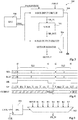
- Figure 4 is a timing diagram representing examples of the signals NFC, RAC, BB, of S-box access operations OP, and of the output value OUTPUT, during a series of accesses SA1 and SA2 using the circuit of Figure 3 .
- the value of NFC is randomly generated to equal 2
- the value of RAC is randomly generated to equal 5.
- the number NF of dummy S-box operations in the series SA1 is equal to 3.
- the total number of S-box accesses in any series is equal to NF+1
- the result of the operation NF*RAC is for example a 3-bit value that may assume a value between 0 and NF, where 0 represents the first access of the series, and NF represents the last access of the series.
- the position of the real access operation is equal to a logic AND applied bit by bit to the values "011" and "101", which gives "001", corresponding to the second access of the series.
- the busy bit BB for example goes high at a time t0 at the start of the series of access operations SA1, which comprises four S-box accesses corresponding, in sequence, to: a dummy access FA; a real access RA1; a dummy access FA; and a dummy access FA.
- the busy bit BB then for example goes low at the time t1 following the last access, and the output value OUTPUT becomes equal to the result of the real access RA1 a short time later.
- the value of NFC is randomly generated to equal 1
- the value of RAC is randomly generated to equal 4.
- the number NF of dummy S-box operations in the series SA2 is equal to 1
- the position of the real access operation in the series SA2 is equal to a logic AND applied bit by bit to the values "001" and "100", which gives "000", corresponding to the first access of the series.
- the busy bit BB for example goes high at a time t2 at the start of the series of access operations SA2, which comprises two S-box accesses corresponding, in sequence, to: a real access RA2; and a dummy access FA.
- the busy bit BB then for example goes low at the time t3 following the last access, and the output value OUTPUT becomes equal to the result of the real access RA2 a short time later.
- Figure 5 schematically illustrates part of the S-box input circuit 304 of Figure 3 in more detail according to an example embodiment.
- the circuit 304 for example comprises a multiplexer 502 having N+1 inputs for receiving the N random values from the random number generator 306, and the real input value INPUT.
- N is equal to 7, and the 7 random values are labelled R1 to R7.
- the circuit 304 also for example comprises a selection circuit (SEL) 504 that generates a selection signal for controlling the multiplexer 502 based on the control signal CTRL from the random number generator 306.
- the selection circuit 504 for example receives a clock signal CLK indicating the period of each access operation such that the selection signal can be updated at the appropriate time.
- CLK clock signal
- the random values R1 to R7 are for example refreshed after each series of S-box accesses, in other words each time the input data INPUT is updated.
- Figures 3 and 5 corresponds to a hardware implementation.
- the method of performing an S-box access described herein could be implemented in software, as will now be described in more detail with reference to Figures 6 and 7 .
- FIG. 6 schematically illustrates a processing system 600 according to an example embodiment of the present disclosure.
- the system 600 for example comprises a processing device (P) 602 coupled via a bus 604 to a memory 606 storing one or more S-boxes (S-BOXES).
- the memory 606 is for example a non-volatile memory (NVM).
- the system 600 also for example comprises, coupled to the bus 604, a volatile memory 608, which is for example a RAM (random access memory), an input/output interface (I/O INTERFACE) 610, and a random number generator (RNG) 612.
- the processing device 602 for example comprises one or more processing cores under control of instructions stored in an instruction memory, for example the memory 606 and/or 608.
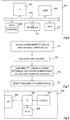
- Figure 7 is a flow diagram illustrating operations in a method of performing an S-box access according to an example embodiment of the present disclosure, and using the processing system of Figure 6 .
- N random input values and one real input value are for example loaded into the working memory of the processing device 602, the working memory for example corresponding to the RAM 608.
- the random values are for example generated by the random number generator 612, whereas the real input value is for example a result, stored to the RAM 608, of a previous operation performed by the processing device 602 involving a secret key.
- the random values NFC and RAC are generated, for example based on random values provided by the generator 612. These values are for example stored in the RAM 608.
- the processing device 602 performs 2 NFC S-box accesses, wherein one of these accesses corresponds to a real access based on the real input value, and 2 NFC - 1 of these accesses correspond to dummy accesses, and wherein the real access is positioned with respect to the dummy accesses based on the value RAC.
- Each access is for example performed by addressing the non-volatile memory 606, and in particular a lookup table stored in the non-volatile memory 606. The result of each access is stored to memory, such as to the RAM 608.
- the result corresponding to the real access is selected to be used in the cryptographic algorithm, based on the random values NFC and RAC.
- the processing device 602 selects in the RAM 608, based on the values of the random values NFC and RAC, an address corresponding to the storage location of the result of the real substitution operation.
- Figure 8 schematically illustrates a cryptographic device 800 according to an example embodiment.
- the device 800 for example comprises a processing device (P) 802 corresponding to the host processor of the cryptographic device 800.
- the processing device 802 is for example in communication with a cryptographic circuit 804 (CRYPTO), which for example corresponds to the circuit 300 of Figure 3 , or to some or all of the components of the processing system 600.
- the cryptographic device 800 also for example comprises a memory (MEM) 806 and an input/output interface (I/O) 808 in communication with processing device 802.
- MEM memory
- I/O input/output interface
- the device 800 for example corresponds to an integrated circuit card (often known as a "smart card"), portable electronics device or other type of electronics device in which a cryptographic function is to be realised.
- the input/output interface 808 may correspond to an NFC (near-field communication) interface.
- An advantage of the embodiments described herein is that the discovery of a secret key manipulated during substitution operations of a cryptographic algorithm using side channel methods can be rendered considerably more difficult. Indeed, by performing dummy accesses and positioning the real S-box access at a random position with respect to the dummy S-box accesses, this creates a dissymmetry of the leakages during each real S-box access, and it becomes very difficult for a meaningful correlation to be determined between side channel signals during the S-box accesses and the value of the secret key. Furthermore, the discovery of the secret key can be rendered even more difficult by additionally randomising the number of dummy substitution operations performed for each real substitution operation.
- An advantage of the hardware implementation of Figures 3 and 5 is that switching between dummy and real S-box accesses can be performed relatively rapidly, leading to a relatively small time overhead for the additional S-box accesses.
- NFC and RAC have respectively 2 and 3 bits
- these values could have a different number of bits depending on the value of N.
Landscapes
- Engineering & Computer Science (AREA)
- Computer Security & Cryptography (AREA)
- Computer Networks & Wireless Communication (AREA)
- Signal Processing (AREA)
- Physics & Mathematics (AREA)
- General Physics & Mathematics (AREA)
- Theoretical Computer Science (AREA)
- Storage Device Security (AREA)
Abstract
Description
- This application claims the priority benefit of French patent application number
18/51644, filed on February 26, 2018 - The present disclosure relates to the field of electronic circuits, and in particular to a device and method for accessing substitution tables during a cryptographic operation.
- Substitution tables, also known as S-boxes, define a data substitution operation performed during cryptographic algorithms. The purpose of this data substitution is to obscure the relationship between the secret key and the cipher text, and thus render it harder for the secret key to be discovered.
- One technique used by hackers wishing to recover the secret key processed by a cryptographic device is to monitor signals on side channels in order to extract certain information relating, for example, to the power consumption or the timing in the device during the execution of a cryptographic algorithm. The manipulation of the secret key during substitution operations is often targeted by hackers using side channel methods due to the relative visibility of substitution operations.
- Some solutions have been proposed providing a limited degree of protection against the use of side channel methods. There is however a need in the art for solutions providing greater protection.
- It is an aim of embodiments of the present description to at least partially address one or more needs in the prior art.
- According to one aspect, there is provided a method of implementing, by a cryptographic circuit, a substitution operation of a cryptographic algorithm, the method comprising: performing, for each substitution operation of the cryptographic algorithm, a series of substitution operations of which: one is a real substitution operation corresponding to the substitution operation of the cryptographic algorithm; and one or more others are dummy substitution operations, wherein the position of the real substitution operation among the one or more dummy substitution operations in each of said series is selected randomly.
- According to one embodiment, each substitution operation comprises addressing a memory location of a memory based on input data and reading a data value at said memory location to provide output data.
- According to one embodiment, each series of substitution operations comprises a number m of substitution operations, where m is an integer selected randomly for each series.
- According to one embodiment, the method further comprises generating a first random value for a first series of substitution operations, and using the first random value to select the number m of substitution operations in said first series.
- According to one embodiment, the method further comprises generating a second random value for a first series of substitution operations, and using the second random value to select the position of the real substitution operation among the one or more dummy substitution operations in said first series.
- According to one embodiment, performing each series of substitution operations comprises: loading a real input value and N random input values; and supplying, on consecutive S-box access operations, said real input value and m-1 of said random input values to an S-box, the order that the real input value is supplied with respect to m-1 random input values being selected based on the second random value.
- According to one embodiment, the method further comprises, for each series of substitution operations, storing an output value of each substitution operation, and selecting the output value corresponding to said real substitution operation based on said second random value.
- According to a further aspect, there is provided a non-transitory storage medium storing a computer program configured, when executed by a processing device, to implement the above method.
- According to a further aspect, there is provided a cryptographic circuit comprising: a memory circuit storing a substitution table for implementing a substitution operation of a cryptographic algorithm; and one or more circuits configured to perform, for each substitution operation of the cryptographic algorithm, a series of substitution operations using said substitution table, each series of substitution operations comprising: a real substitution operation corresponding to the substitution operation of the cryptographic algorithm; and one or more dummy substitution operations, the one or more circuits being configured to randomly select the position of the real substitution operation among the one or more dummy substitution operations in each of said series.
- According to one embodiment, the cryptographic circuit further comprises a random number generator configured to generate, for each of said series, a first random value for randomly selecting the number of dummy substitution operations to be performed in the series.
- According to one embodiment, the random number generator is further configured to generate, for each of said series, a second random value for randomly selecting the position of the real substitution operation among the dummy substitution operations.
- According to one embodiment, the cryptographic circuit further comprises a memory for storing a result of the substitution operations of each of said series.
- According to one embodiment, the one or more circuits is an S-box input circuit comprising: one or more registers configured to store a real input value corresponding to said real substitution operation and N random input values; and one or more multiplexers configured to select, for each substitution operation of each series, a value among said real input value and said N random input values to form an input to the memory circuit storing said substitution table.
- According to one embodiment, the cryptographic circuit further comprises a selection circuit configured to generate a selection signal for controlling the one or multiplexers to perform the selection of said value for each substitution operation.
- According to one embodiment, the one or more circuits comprise one or more processing devices under control of instructions stored in an instruction memory to select, for each substitution operation of each series, either said real input value or a random input value to form an input to the memory circuit storing said substitution table.
- The foregoing and other features and advantages will become apparent from the following detailed description of embodiments, given by way of illustration and not limitation with reference to the accompanying drawings, in which:
-
Figure 1 schematically illustrates a circuit for executing a cryptographic algorithm involving substitution operations according to an example embodiment; -
Figure 2 schematically illustrates an S-box according to an example embodiment; -
Figure 3 schematically illustrates a cryptographic circuit for performing S-box accesses according to an example embodiment of the present disclosure; -
Figure 4 is a timing diagram illustrating an example of signals in the circuit ofFigure 3 ; -
Figure 5 schematically illustrates part of an S-box input circuit ofFigure 3 in more detail according to an example embodiment of the present disclosure; -
Figure 6 schematically illustrates a processing system for performing S-box accesses according to an example embodiment of the present disclosure; -
Figure 7 is a flow diagram representing operations in a method of performing an S-box access according to an example embodiment of the present disclosure; and -
Figure 8 schematically illustrates a cryptographic device according to an example embodiment of the present disclosure. - Throughout the present disclosure, the term "connected" is used to designate a direct electrical connection between circuit elements, whereas the term "coupled" is used to designate an electrical connection between circuit elements that may be direct, or may be via one or more intermediate elements such as multiplexers, buffers, etc.
- Furthermore, throughout the present disclosure, the following terms will be considered to have the following definitions:
- "cryptographic algorithm" - any series of operations performed by a device that involves the manipulation of a secret value, such as a secret key, which is to be hidden from the world outside the device. Examples of cryptographic algorithms include algorithms for encrypting or decrypting plaintext/cipher-text based on a secret key, for generating a message authentication code (MAC) or other form of digital signature based on a secret algorithm and/or key, or any other type of secretive operation;
- "substitution operation" or "S-box access" - an operation of a cryptographic algorithm in which an output data value is generated based on an input data value using a substitution table, i.e. an S-box. The input and output values may have the same, or a different, number of bits. This operation is for example performed using a lookup table (LUT) stored in a memory, and the values defined in the lookup table may be fixed, or could be updated dynamically;
- "real substitution operation" - a substitution operation defined by the cryptographic algorithm that is being executed, which is for example a useful operation in that the result of the substitution will contribute towards the calculation of the output data of the cryptographic algorithm; and
- "dummy substitution operation" - a fake or false substitution operation performed in the same manner as a real substitution operation, but which is superfluous as it is performed in addition to the real substitution operations defined by the cryptographic algorithm. While the result of each dummy substitution operation may be stored to memory, it is not useful in that the result serves no purpose in relation with the cryptographic algorithm and can be discarded. As described herein, the dummy substitution operations are for example performed based on random input data.
-
Figure 1 schematically illustrates acryptographic circuit 100 according to an example embodiment. Thecircuit 100 for example receives as inputs a message (MESSAGE) to be processed and a secret key (KEY). For example, the message corresponds to plaintext to be encrypted by thecircuit 100 using the secret key, to cipher-text to be decrypted by thecircuit 100 using the secret key, or to data that is to be signed by thecircuit 100 by generating a digital signature, such as a MAC (message authentication code) based on the key. - The
circuit 100 comprises a series of hardware modules implementingvarious operations Figure 1 , theoperation 104 corresponds to a substitution operation involving one or more substitution tables (S-BOXES). -
Figure 2 schematically illustrates an example of an S-box used during the DES (data encryption standard) algorithm. As known to those skilled in the art, the DES encryption algorithm involves 8 S-boxes S1 to S8, each of which is unique.Figure 2 illustrates the DES S-box S1. - An S-box access according to the DES encryption algorithm involves inputting 6 input bits (INPUT) b5 to b0, and outputting 4 output bits (OUTPUT) b3 to b0. The S-box S1 is in the form of a lookup table having 16 columns and 4 rows. The bits b5 and b0 of the input value are for example used to select a row of the table, and the bits b4 to b1 of the input value are for example used to select a column of the table. The 4-bit value stored in the selected row and column forms the output value of the S-box.
- Of course
Figure 2 illustrates only one example of an S-box, and the principles described in the present disclosure could be applied to any type of S-box in which input data is substituted in order to generate output data based on a table of stored values. -
Figure 3 schematically illustrates acryptographic circuit 300 for implementing S-box access operations according to an example embodiment of the present disclosure. Thecircuit 300 for example forms part of thecircuit 100 ofFigure 1 . - The
circuit 300 comprises an S-box 302 receiving input data SB_IN, and providing output data SB_OUT. The S-box 302 is for example implemented by a non-volatile memory, in which the input data SB_IN provides an address input to the memory, and the output data SB_OUT corresponds to the data value stored at the addressed location in the memory. - The S-
box 302 for example corresponds to the S-box S1 ofFigure 2 , or to any other S-box of the DES encryption standard. Alternatively, the S-box 302 could correspond to an S-box used in the TDES (Triple DES), AES (advanced encryption standard) or SM4 (formerly known as SMS4) encryption standards, or in any other encryption standard. - The
circuit 300 further comprises an S-box input circuit (S-BOX INPUT CIRCUIT) 304 receiving an input value INPUT corresponding to a real substitution operation to be performed in relation with a cryptographic algorithm. For example, the input value INPUT is the result of an operation performed on the message data and the key data ofFigure 1 . - The S-
box input circuit 304 also receives N random input values (N x RANDOM), and a control signal CTRL, from a random number generator (RNG) 306. Thegenerator 306 is for example a pseudo-random number generator or a true random number generator. - The
circuit 300 further comprises an S-box output circuit (S-BOX OUTPUT CIRCUIT) 308 that receives the output data SB_OUT from the S-box 302 and also the control signal CTRL from therandom number generator 306. The S-box output circuit 308 is for example coupled to an output register (OUTPUT REGISTER) 310, which provides output data OUTPUT representing the result of the S-box access operation. In some embodiments, theinput circuit 304 and theoutput circuit 308 assert a busy bit (BB) to indicate to a host system the periods in which the S-box 302 is occupied. - In operation, for each S-box access operation to be performed in view of a corresponding substitution operation of a cryptographic algorithm, a series of S-box accesses is performed by S-
box input circuit 304. Only one of these accesses corresponds to the real S-box access relating to the substitution operation of the cryptographic algorithm. The other one or more S-box accesses correspond to dummy accesses based on the random values provided by thegenerator 306, the results of which are discarded. - For example, each time an S-box access is to be performed, the real input data value and N random input values are loaded into the S-
box input circuit 304, where N is a positive integer for example equal to at least 7 in some embodiments. The control signal CTRL generated by therandom number generator 306 for example comprises a value NFC indicating the number of dummy accesses to be implemented, and a value RAC indicating the position of the real access with respect to the dummy accesses. - For example, in one embodiment the value NFC is a 2-bit value, and the value RAC is a 3-bit value. The number NF of dummy S-box accesses in each series of S-box accesses is for example equal to:

- By randomly generating the value of NFC for each series of S-box accesses, the processing time for each real S-box access will be variable. Thus, as the duration of each S-box access is no longer predictable, the busy bit BB for example indicates to the host processing system the time periods during which the S-
box 302 is occupied. - According to some embodiments, the S-
box output circuit 308 stores each of the output values SB_OUT from the S-box 302 during each access operation to theoutput register 310. Furthermore, thecircuit 308 for example selects the real output value to form the output value OUTPUT of theregister 310 based on the control signal CTRL. In particular, the value NFC indicates the number of dummy output values provided by the S-box 302, and the value RAC indicates the position of the real output value with respect to the dummy output values. - Operation of the circuit of
Figure 3 will now be described in more detail with reference toFigure 4 . -
Figure 4 is a timing diagram representing examples of the signals NFC, RAC, BB, of S-box access operations OP, and of the output value OUTPUT, during a series of accesses SA1 and SA2 using the circuit ofFigure 3 . - In the example of
Figure 4 , during the series of accesses SA1, the value of NFC is randomly generated to equal 2, and the value of RAC is randomly generated toequal 5. Thus the number NF of dummy S-box operations in the series SA1 is equal to 3. The total number of S-box accesses in any series is equal to NF+1, and the result of the operation NF*RAC is for example a 3-bit value that may assume a value between 0 and NF, where 0 represents the first access of the series, and NF represents the last access of the series. Thus, in the example of the series of accesses SA1, the position of the real access operation is equal to a logic AND applied bit by bit to the values "011" and "101", which gives "001", corresponding to the second access of the series. - The busy bit BB for example goes high at a time t0 at the start of the series of access operations SA1, which comprises four S-box accesses corresponding, in sequence, to: a dummy access FA; a real access RA1; a dummy access FA; and a dummy access FA. The busy bit BB then for example goes low at the time t1 following the last access, and the output value OUTPUT becomes equal to the result of the real access RA1 a short time later.
- During the series of S-box accesses SA2, the value of NFC is randomly generated to equal 1, and the value of RAC is randomly generated to
equal 4. Thus the number NF of dummy S-box operations in the series SA2 is equal to 1, and the position of the real access operation in the series SA2 is equal to a logic AND applied bit by bit to the values "001" and "100", which gives "000", corresponding to the first access of the series. - The busy bit BB for example goes high at a time t2 at the start of the series of access operations SA2, which comprises two S-box accesses corresponding, in sequence, to: a real access RA2; and a dummy access FA. The busy bit BB then for example goes low at the time t3 following the last access, and the output value OUTPUT becomes equal to the result of the real access RA2 a short time later.
-
Figure 5 schematically illustrates part of the S-box input circuit 304 ofFigure 3 in more detail according to an example embodiment. Thecircuit 304 for example comprises a multiplexer 502 having N+1 inputs for receiving the N random values from therandom number generator 306, and the real input value INPUT. In the example ofFigure 5 , N is equal to 7, and the 7 random values are labelled R1 to R7. - The
circuit 304 also for example comprises a selection circuit (SEL) 504 that generates a selection signal for controlling the multiplexer 502 based on the control signal CTRL from therandom number generator 306. Theselection circuit 504 for example receives a clock signal CLK indicating the period of each access operation such that the selection signal can be updated at the appropriate time. As indicated above, depending on the number of dummy access operations in a given series of S-box accesses, the number of these random input values used during this series of accesses will vary between none and N. The random values R1 to R7 are for example refreshed after each series of S-box accesses, in other words each time the input data INPUT is updated. - The example of
Figures 3 and 5 corresponds to a hardware implementation. In alternative embodiments, the method of performing an S-box access described herein could be implemented in software, as will now be described in more detail with reference toFigures 6 and 7 . -
Figure 6 schematically illustrates aprocessing system 600 according to an example embodiment of the present disclosure. Thesystem 600 for example comprises a processing device (P) 602 coupled via abus 604 to amemory 606 storing one or more S-boxes (S-BOXES). Thememory 606 is for example a non-volatile memory (NVM). Thesystem 600 also for example comprises, coupled to thebus 604, avolatile memory 608, which is for example a RAM (random access memory), an input/output interface (I/O INTERFACE) 610, and a random number generator (RNG) 612. Theprocessing device 602 for example comprises one or more processing cores under control of instructions stored in an instruction memory, for example thememory 606 and/or 608. -
Figure 7 is a flow diagram illustrating operations in a method of performing an S-box access according to an example embodiment of the present disclosure, and using the processing system ofFigure 6 . - In an
operation 701, N random input values and one real input value are for example loaded into the working memory of theprocessing device 602, the working memory for example corresponding to theRAM 608. The random values are for example generated by therandom number generator 612, whereas the real input value is for example a result, stored to theRAM 608, of a previous operation performed by theprocessing device 602 involving a secret key. - In an
operation 702, the random values NFC and RAC are generated, for example based on random values provided by thegenerator 612. These values are for example stored in theRAM 608. - In an
operation 703, theprocessing device 602 performs 2 NFC S-box accesses, wherein one of these accesses corresponds to a real access based on the real input value, and 2 NFC - 1 of these accesses correspond to dummy accesses, and wherein the real access is positioned with respect to the dummy accesses based on the value RAC. Each access is for example performed by addressing thenon-volatile memory 606, and in particular a lookup table stored in thenon-volatile memory 606. The result of each access is stored to memory, such as to theRAM 608. - In
operation 704, the result corresponding to the real access is selected to be used in the cryptographic algorithm, based on the random values NFC and RAC. For example, theprocessing device 602 selects in theRAM 608, based on the values of the random values NFC and RAC, an address corresponding to the storage location of the result of the real substitution operation. -
Figure 8 schematically illustrates acryptographic device 800 according to an example embodiment. - The
device 800 for example comprises a processing device (P) 802 corresponding to the host processor of thecryptographic device 800. Theprocessing device 802 is for example in communication with a cryptographic circuit 804 (CRYPTO), which for example corresponds to thecircuit 300 ofFigure 3 , or to some or all of the components of theprocessing system 600. Thecryptographic device 800 also for example comprises a memory (MEM) 806 and an input/output interface (I/O) 808 in communication withprocessing device 802. - The
device 800 for example corresponds to an integrated circuit card (often known as a "smart card"), portable electronics device or other type of electronics device in which a cryptographic function is to be realised. In some embodiments, the input/output interface 808 may correspond to an NFC (near-field communication) interface. - An advantage of the embodiments described herein is that the discovery of a secret key manipulated during substitution operations of a cryptographic algorithm using side channel methods can be rendered considerably more difficult. Indeed, by performing dummy accesses and positioning the real S-box access at a random position with respect to the dummy S-box accesses, this creates a dissymmetry of the leakages during each real S-box access, and it becomes very difficult for a meaningful correlation to be determined between side channel signals during the S-box accesses and the value of the secret key. Furthermore, the discovery of the secret key can be rendered even more difficult by additionally randomising the number of dummy substitution operations performed for each real substitution operation.
- An advantage of the hardware implementation of
Figures 3 and 5 is that switching between dummy and real S-box accesses can be performed relatively rapidly, leading to a relatively small time overhead for the additional S-box accesses. - Having thus described at least one illustrative embodiment, various alterations, modifications and improvements will readily occur to those skilled in the art. For example, it will be apparent to those skilled in the art that the circuit of
Figure 5 implementing the S-box input circuit is merely one example, and that many alternative implementations would be possible. - Furthermore, while an example has been provided in which the values NFC and RAC have respectively 2 and 3 bits, it will be apparent to those skilled in the art that these values could have a different number of bits depending on the value of N.
- Furthermore, while embodiments have been described based on a single S-box, certain cryptographic algorithms, such as DES, use a plurality of S-boxes in parallel. The embodiments described herein could also be applied to each of a plurality of S-boxes operating in parallel.
- Furthermore, it will be apparent to those skilled in the art that the various features described in relation with the embodiments of
Figures 3 and6 could be combined, in alternative embodiments, in any combination. For example, it would be possible to implement the S-box access method of the present disclosure using a combination of hardware and software.
Claims (15)
- A method of implementing, by a cryptographic circuit (300, 600), a substitution operation of a cryptographic algorithm, the method comprising:
performing, for each substitution operation of the cryptographic algorithm, a series of consecutive substitution operations of which:one is a real substitution operation corresponding to the substitution operation of the cryptographic algorithm; andone or more others are dummy substitution operations, wherein the position of the real substitution operation among the one or more dummy substitution operations in each of said series is selected randomly. - The method of claim 1, wherein each substitution operation comprises addressing a memory location of a memory (302, 606) based on input data (SB_IN) and reading a data value at said memory location to provide output data (SB_OUT).
- The method of claim 1 or 2, wherein each series of substitution operations comprises a number m of substitution operations of which m-1 are dummy substitution operations, where m is an integer selected randomly for each series.
- The method of claim 3, further comprising generating a first random value (NFC) for a first series of substitution operations, and using the first random value (NFC) to select the number m of substitution operations in said first series.
- The method of any of claims 1 to 4, further comprising generating a second random value (RAC) for a first series of substitution operations, and using the second random value to select the position of the real substitution operation among the one or more dummy substitution operations in said first series.
- The method of claim 5, wherein performing each series of substitution operations comprises:loading a real input value and N random input values; andsupplying, on consecutive S-box access operations, said real input value and m-1 of said random input values to an S-box (302, 606), wherein the order that the real input value is supplied with respect to m-1 random input values is selected based on the second random value (RAC).
- The method of claim 5 or 6, further comprising, for each series of substitution operations, storing an output value (SB_OUT) of each substitution operation, and selecting the output value corresponding to said real substitution operation based on said second random value (RAC).
- A non-transitory storage medium storing a computer program configured, when executed by a processing device (602), to implement the method of any of claims 1 to 7.
- A cryptographic circuit comprising:a memory circuit (302, 606) storing a substitution table (S-BOXES) for implementing a substitution operation of a cryptographic algorithm; andone or more circuits (304, 602) configured to perform, for each substitution operation of the cryptographic algorithm, a series of consecutive substitution operations using said substitution table (S-BOX), each series of consecutive substitution operations comprising:a real substitution operation corresponding to the substitution operation of the cryptographic algorithm; andone or more dummy substitution operations, wherein the one or more circuits are configured to randomly select the position of the real substitution operation among the one or more dummy substitution operations in each of said series.
- The cryptographic circuit of claim 9, further comprising a random number generator (306, 612) configured to generate, for each of said series, a first random value (NFC) for randomly selecting the number m of substitution operations, of which m-11 are dummy substitution operations to be performed in the series.
- The cryptographic circuit of claim 10, wherein the random number generator (306, 612) is further configured to generate, for each of said series, a second random value (RAC) for randomly selecting the position of the real substitution operation among the dummy substitution operations.
- The cryptographic circuit of any of claims 9 to 11, further comprising a memory (310, 608) for storing a result of the substitution operations of each of said series.
- The cryptographic circuit of any of claims 9 to 12, wherein the one or more circuits is an S-box input circuit (304) comprising:one or more registers configured to store a real input value corresponding to said real substitution operation and N random input values; andone or more multiplexers (502) configured to select, for each substitution operation of each series, a value among said real input value and said N random input values to form an input to the memory circuit (302) storing said substitution table (S-BOXES).
- The cryptographic circuit of claim 13, further comprising a selection circuit (504) configured to generate a selection signal for controlling the one or multiplexers (502) to perform the selection of said value for each substitution operation.
- The cryptographic circuit of any of claims 9 to 12, wherein the one or more circuits comprise one or more processing devices (602) under control of instructions stored in an instruction memory (606, 608) to select, for each substitution operation of each series, either said real input value or a random input value to form an input to the memory circuit (606) storing said substitution table (S-BOXES).
Applications Claiming Priority (1)
| Application Number | Priority Date | Filing Date | Title |
|---|---|---|---|
| FR1851644A FR3078419A1 (en) | 2018-02-26 | 2018-02-26 | METHOD AND CIRCUIT FOR REALIZING A SUBSTITUTE OPERATION |
Publications (2)
| Publication Number | Publication Date |
|---|---|
| EP3531401A1 true EP3531401A1 (en) | 2019-08-28 |
| EP3531401B1 EP3531401B1 (en) | 2022-10-19 |
Family
ID=62948195
Family Applications (1)
| Application Number | Title | Priority Date | Filing Date |
|---|---|---|---|
| EP19157873.1A Active EP3531401B1 (en) | 2018-02-26 | 2019-02-18 | Method and circuit for performing a substitution operation |
Country Status (2)
| Country | Link |
|---|---|
| EP (1) | EP3531401B1 (en) |
| FR (1) | FR3078419A1 (en) |
Cited By (1)
| Publication number | Priority date | Publication date | Assignee | Title |
|---|---|---|---|---|
| CN113507357A (en) * | 2021-07-08 | 2021-10-15 | 无锡沐创集成电路设计有限公司 | Realization method and circuit module compatible with SM4 and AES algorithm S box |
Citations (2)
| Publication number | Priority date | Publication date | Assignee | Title |
|---|---|---|---|---|
| US20110296198A1 (en) * | 2010-05-27 | 2011-12-01 | Kabushiki Kaisha Toshiba | Cryptographic processing apparatus and ic card |
| FR2985624A1 (en) * | 2012-01-11 | 2013-07-12 | Inside Secure | ENCRYPTION METHOD PROTECTED AGAINST AUXILIARY CHANNEL ATTACKS |
Family Cites Families (1)
| Publication number | Priority date | Publication date | Assignee | Title |
|---|---|---|---|---|
| FR2873523B1 (en) * | 2004-07-22 | 2007-08-10 | Sagem | METHOD AND DEVICE FOR PERFORMING A CRYPTOGRAPHIC CALCULATION |
-
2018
- 2018-02-26 FR FR1851644A patent/FR3078419A1/en not_active Withdrawn
-
2019
- 2019-02-18 EP EP19157873.1A patent/EP3531401B1/en active Active
Patent Citations (2)
| Publication number | Priority date | Publication date | Assignee | Title |
|---|---|---|---|---|
| US20110296198A1 (en) * | 2010-05-27 | 2011-12-01 | Kabushiki Kaisha Toshiba | Cryptographic processing apparatus and ic card |
| FR2985624A1 (en) * | 2012-01-11 | 2013-07-12 | Inside Secure | ENCRYPTION METHOD PROTECTED AGAINST AUXILIARY CHANNEL ATTACKS |
Cited By (2)
| Publication number | Priority date | Publication date | Assignee | Title |
|---|---|---|---|---|
| CN113507357A (en) * | 2021-07-08 | 2021-10-15 | 无锡沐创集成电路设计有限公司 | Realization method and circuit module compatible with SM4 and AES algorithm S box |
| CN113507357B (en) * | 2021-07-08 | 2022-03-11 | 无锡沐创集成电路设计有限公司 | Realization method and circuit module compatible with SM4 and AES algorithm S box |
Also Published As
| Publication number | Publication date |
|---|---|
| FR3078419A1 (en) | 2019-08-30 |
| EP3531401B1 (en) | 2022-10-19 |
Similar Documents
| Publication | Publication Date | Title |
|---|---|---|
| EP3531613B1 (en) | Method and circuit for implementing a substitution table | |
| JP6244429B2 (en) | Stream cipher encryption apparatus, stream cipher decryption apparatus, stream cipher encryption method, stream cipher decryption method, and program | |
| US11824969B2 (en) | Method and circuit for performing a substitution operation | |
| CN105940439A (en) | Countermeasures against side-channel attacks on cryptographic algorithms using permutations | |
| US8010587B2 (en) | Random number generator | |
| US9288040B2 (en) | Encryption device | |
| US9565018B2 (en) | Protecting cryptographic operations using conjugacy class functions | |
| KR20120038104A (en) | Apparatus and method for generating random data | |
| US20110200190A1 (en) | Cryptography processing device and cryptography processing method | |
| JPWO2008013083A1 (en) | Pseudorandom number generator, stream cipher processor, and program | |
| US20170063524A1 (en) | Protection of a rijndael algorithm | |
| US10530567B2 (en) | Encryption device and memory device | |
| EP3531612B1 (en) | Method and device for performing substitution table operations | |
| EP3531401B1 (en) | Method and circuit for performing a substitution operation | |
| EP1629626B1 (en) | Method and apparatus for a low memory hardware implementation of the key expansion function | |
| US20240113871A1 (en) | Encryption processing apparatus, encryption processing method for encryption processing apparatus, and storage medium | |
| JP6167721B2 (en) | ENCRYPTION DEVICE, DECRYPTION DEVICE, ENCRYPTION METHOD, DECRYPTION METHOD, AND PROGRAM | |
| JP2006025366A (en) | Encryption apparatus and semiconductor integrated circuit | |
| KR100494560B1 (en) | Real time block data encryption/decryption processor using Rijndael block cipher and method therefor | |
| CA2592703A1 (en) | Communication system and communication method | |
| KR100511684B1 (en) | The pseudo random number generator | |
| KR20060110383A (en) | Multimode Encryption Device for Network Security Processors | |
| US20190384894A1 (en) | Intrinsic authentication of program code | |
| JP2005529365A (en) | AES mix column conversion | |
| KR20180021473A (en) | Encryption device |
Legal Events
| Date | Code | Title | Description |
|---|---|---|---|
| PUAI | Public reference made under article 153(3) epc to a published international application that has entered the european phase |
Free format text: ORIGINAL CODE: 0009012 |
|
| STAA | Information on the status of an ep patent application or granted ep patent |
Free format text: STATUS: REQUEST FOR EXAMINATION WAS MADE |
|
| 17P | Request for examination filed |
Effective date: 20190218 |
|
| AK | Designated contracting states |
Kind code of ref document: A1 Designated state(s): AL AT BE BG CH CY CZ DE DK EE ES FI FR GB GR HR HU IE IS IT LI LT LU LV MC MK MT NL NO PL PT RO RS SE SI SK SM TR |
|
| AX | Request for extension of the european patent |
Extension state: BA ME |
|
| STAA | Information on the status of an ep patent application or granted ep patent |
Free format text: STATUS: EXAMINATION IS IN PROGRESS |
|
| 17Q | First examination report despatched |
Effective date: 20191210 |
|
| GRAP | Despatch of communication of intention to grant a patent |
Free format text: ORIGINAL CODE: EPIDOSNIGR1 |
|
| STAA | Information on the status of an ep patent application or granted ep patent |
Free format text: STATUS: GRANT OF PATENT IS INTENDED |
|
| RIC1 | Information provided on ipc code assigned before grant |
Ipc: H04L 9/00 20060101ALI20211115BHEP Ipc: H04L 9/06 20060101ALI20211115BHEP Ipc: G09C 1/00 20060101AFI20211115BHEP |
|
| INTG | Intention to grant announced |
Effective date: 20211207 |
|
| GRAJ | Information related to disapproval of communication of intention to grant by the applicant or resumption of examination proceedings by the epo deleted |
Free format text: ORIGINAL CODE: EPIDOSDIGR1 |
|
| STAA | Information on the status of an ep patent application or granted ep patent |
Free format text: STATUS: EXAMINATION IS IN PROGRESS |
|
| INTC | Intention to grant announced (deleted) | ||
| GRAP | Despatch of communication of intention to grant a patent |
Free format text: ORIGINAL CODE: EPIDOSNIGR1 |
|
| STAA | Information on the status of an ep patent application or granted ep patent |
Free format text: STATUS: GRANT OF PATENT IS INTENDED |
|
| INTG | Intention to grant announced |
Effective date: 20220516 |
|
| GRAS | Grant fee paid |
Free format text: ORIGINAL CODE: EPIDOSNIGR3 |
|
| GRAA | (expected) grant |
Free format text: ORIGINAL CODE: 0009210 |
|
| STAA | Information on the status of an ep patent application or granted ep patent |
Free format text: STATUS: THE PATENT HAS BEEN GRANTED |
|
| AK | Designated contracting states |
Kind code of ref document: B1 Designated state(s): AL AT BE BG CH CY CZ DE DK EE ES FI FR GB GR HR HU IE IS IT LI LT LU LV MC MK MT NL NO PL PT RO RS SE SI SK SM TR |
|
| REG | Reference to a national code |
Ref country code: GB Ref legal event code: FG4D |
|
| REG | Reference to a national code |
Ref country code: CH Ref legal event code: EP |
|
| REG | Reference to a national code |
Ref country code: IE Ref legal event code: FG4D |
|
| REG | Reference to a national code |
Ref country code: AT Ref legal event code: REF Ref document number: 1526057 Country of ref document: AT Kind code of ref document: T Effective date: 20221115 |
|
| REG | Reference to a national code |
Ref country code: DE Ref legal event code: R096 Ref document number: 602019020698 Country of ref document: DE |
|
| REG | Reference to a national code |
Ref country code: LT Ref legal event code: MG9D |
|
| REG | Reference to a national code |
Ref country code: NL Ref legal event code: MP Effective date: 20221019 |
|
| REG | Reference to a national code |
Ref country code: AT Ref legal event code: MK05 Ref document number: 1526057 Country of ref document: AT Kind code of ref document: T Effective date: 20221019 |
|
| PG25 | Lapsed in a contracting state [announced via postgrant information from national office to epo] |
Ref country code: NL Free format text: LAPSE BECAUSE OF FAILURE TO SUBMIT A TRANSLATION OF THE DESCRIPTION OR TO PAY THE FEE WITHIN THE PRESCRIBED TIME-LIMIT Effective date: 20221019 |
|
| PG25 | Lapsed in a contracting state [announced via postgrant information from national office to epo] |
Ref country code: SE Free format text: LAPSE BECAUSE OF FAILURE TO SUBMIT A TRANSLATION OF THE DESCRIPTION OR TO PAY THE FEE WITHIN THE PRESCRIBED TIME-LIMIT Effective date: 20221019 Ref country code: PT Free format text: LAPSE BECAUSE OF FAILURE TO SUBMIT A TRANSLATION OF THE DESCRIPTION OR TO PAY THE FEE WITHIN THE PRESCRIBED TIME-LIMIT Effective date: 20230220 Ref country code: NO Free format text: LAPSE BECAUSE OF FAILURE TO SUBMIT A TRANSLATION OF THE DESCRIPTION OR TO PAY THE FEE WITHIN THE PRESCRIBED TIME-LIMIT Effective date: 20230119 Ref country code: LT Free format text: LAPSE BECAUSE OF FAILURE TO SUBMIT A TRANSLATION OF THE DESCRIPTION OR TO PAY THE FEE WITHIN THE PRESCRIBED TIME-LIMIT Effective date: 20221019 Ref country code: FI Free format text: LAPSE BECAUSE OF FAILURE TO SUBMIT A TRANSLATION OF THE DESCRIPTION OR TO PAY THE FEE WITHIN THE PRESCRIBED TIME-LIMIT Effective date: 20221019 Ref country code: ES Free format text: LAPSE BECAUSE OF FAILURE TO SUBMIT A TRANSLATION OF THE DESCRIPTION OR TO PAY THE FEE WITHIN THE PRESCRIBED TIME-LIMIT Effective date: 20221019 Ref country code: AT Free format text: LAPSE BECAUSE OF FAILURE TO SUBMIT A TRANSLATION OF THE DESCRIPTION OR TO PAY THE FEE WITHIN THE PRESCRIBED TIME-LIMIT Effective date: 20221019 |
|
| PG25 | Lapsed in a contracting state [announced via postgrant information from national office to epo] |
Ref country code: RS Free format text: LAPSE BECAUSE OF FAILURE TO SUBMIT A TRANSLATION OF THE DESCRIPTION OR TO PAY THE FEE WITHIN THE PRESCRIBED TIME-LIMIT Effective date: 20221019 Ref country code: PL Free format text: LAPSE BECAUSE OF FAILURE TO SUBMIT A TRANSLATION OF THE DESCRIPTION OR TO PAY THE FEE WITHIN THE PRESCRIBED TIME-LIMIT Effective date: 20221019 Ref country code: LV Free format text: LAPSE BECAUSE OF FAILURE TO SUBMIT A TRANSLATION OF THE DESCRIPTION OR TO PAY THE FEE WITHIN THE PRESCRIBED TIME-LIMIT Effective date: 20221019 Ref country code: IS Free format text: LAPSE BECAUSE OF FAILURE TO SUBMIT A TRANSLATION OF THE DESCRIPTION OR TO PAY THE FEE WITHIN THE PRESCRIBED TIME-LIMIT Effective date: 20230219 Ref country code: HR Free format text: LAPSE BECAUSE OF FAILURE TO SUBMIT A TRANSLATION OF THE DESCRIPTION OR TO PAY THE FEE WITHIN THE PRESCRIBED TIME-LIMIT Effective date: 20221019 Ref country code: GR Free format text: LAPSE BECAUSE OF FAILURE TO SUBMIT A TRANSLATION OF THE DESCRIPTION OR TO PAY THE FEE WITHIN THE PRESCRIBED TIME-LIMIT Effective date: 20230120 |
|
| REG | Reference to a national code |
Ref country code: DE Ref legal event code: R097 Ref document number: 602019020698 Country of ref document: DE |
|
| PG25 | Lapsed in a contracting state [announced via postgrant information from national office to epo] |
Ref country code: SM Free format text: LAPSE BECAUSE OF FAILURE TO SUBMIT A TRANSLATION OF THE DESCRIPTION OR TO PAY THE FEE WITHIN THE PRESCRIBED TIME-LIMIT Effective date: 20221019 Ref country code: RO Free format text: LAPSE BECAUSE OF FAILURE TO SUBMIT A TRANSLATION OF THE DESCRIPTION OR TO PAY THE FEE WITHIN THE PRESCRIBED TIME-LIMIT Effective date: 20221019 Ref country code: EE Free format text: LAPSE BECAUSE OF FAILURE TO SUBMIT A TRANSLATION OF THE DESCRIPTION OR TO PAY THE FEE WITHIN THE PRESCRIBED TIME-LIMIT Effective date: 20221019 Ref country code: DK Free format text: LAPSE BECAUSE OF FAILURE TO SUBMIT A TRANSLATION OF THE DESCRIPTION OR TO PAY THE FEE WITHIN THE PRESCRIBED TIME-LIMIT Effective date: 20221019 Ref country code: CZ Free format text: LAPSE BECAUSE OF FAILURE TO SUBMIT A TRANSLATION OF THE DESCRIPTION OR TO PAY THE FEE WITHIN THE PRESCRIBED TIME-LIMIT Effective date: 20221019 |
|
| PLBE | No opposition filed within time limit |
Free format text: ORIGINAL CODE: 0009261 |
|
| STAA | Information on the status of an ep patent application or granted ep patent |
Free format text: STATUS: NO OPPOSITION FILED WITHIN TIME LIMIT |
|
| PG25 | Lapsed in a contracting state [announced via postgrant information from national office to epo] |
Ref country code: SK Free format text: LAPSE BECAUSE OF FAILURE TO SUBMIT A TRANSLATION OF THE DESCRIPTION OR TO PAY THE FEE WITHIN THE PRESCRIBED TIME-LIMIT Effective date: 20221019 Ref country code: AL Free format text: LAPSE BECAUSE OF FAILURE TO SUBMIT A TRANSLATION OF THE DESCRIPTION OR TO PAY THE FEE WITHIN THE PRESCRIBED TIME-LIMIT Effective date: 20221019 |
|
| 26N | No opposition filed |
Effective date: 20230720 |
|
| PG25 | Lapsed in a contracting state [announced via postgrant information from national office to epo] |
Ref country code: MC Free format text: LAPSE BECAUSE OF FAILURE TO SUBMIT A TRANSLATION OF THE DESCRIPTION OR TO PAY THE FEE WITHIN THE PRESCRIBED TIME-LIMIT Effective date: 20221019 |
|
| REG | Reference to a national code |
Ref country code: CH Ref legal event code: PL |
|
| REG | Reference to a national code |
Ref country code: BE Ref legal event code: MM Effective date: 20230228 |
|
| GBPC | Gb: european patent ceased through non-payment of renewal fee |
Effective date: 20230218 |
|
| PG25 | Lapsed in a contracting state [announced via postgrant information from national office to epo] |
Ref country code: LU Free format text: LAPSE BECAUSE OF NON-PAYMENT OF DUE FEES Effective date: 20230218 Ref country code: LI Free format text: LAPSE BECAUSE OF NON-PAYMENT OF DUE FEES Effective date: 20230228 Ref country code: CH Free format text: LAPSE BECAUSE OF NON-PAYMENT OF DUE FEES Effective date: 20230228 |
|
| PG25 | Lapsed in a contracting state [announced via postgrant information from national office to epo] |
Ref country code: SI Free format text: LAPSE BECAUSE OF FAILURE TO SUBMIT A TRANSLATION OF THE DESCRIPTION OR TO PAY THE FEE WITHIN THE PRESCRIBED TIME-LIMIT Effective date: 20221019 |
|
| REG | Reference to a national code |
Ref country code: IE Ref legal event code: MM4A |
|
| PG25 | Lapsed in a contracting state [announced via postgrant information from national office to epo] |
Ref country code: GB Free format text: LAPSE BECAUSE OF NON-PAYMENT OF DUE FEES Effective date: 20230218 |
|
| PG25 | Lapsed in a contracting state [announced via postgrant information from national office to epo] |
Ref country code: IE Free format text: LAPSE BECAUSE OF NON-PAYMENT OF DUE FEES Effective date: 20230218 Ref country code: GB Free format text: LAPSE BECAUSE OF NON-PAYMENT OF DUE FEES Effective date: 20230218 Ref country code: FR Free format text: LAPSE BECAUSE OF NON-PAYMENT OF DUE FEES Effective date: 20230228 |
|
| PG25 | Lapsed in a contracting state [announced via postgrant information from national office to epo] |
Ref country code: BE Free format text: LAPSE BECAUSE OF NON-PAYMENT OF DUE FEES Effective date: 20230228 |
|
| PG25 | Lapsed in a contracting state [announced via postgrant information from national office to epo] |
Ref country code: IT Free format text: LAPSE BECAUSE OF FAILURE TO SUBMIT A TRANSLATION OF THE DESCRIPTION OR TO PAY THE FEE WITHIN THE PRESCRIBED TIME-LIMIT Effective date: 20221019 |
|
| PG25 | Lapsed in a contracting state [announced via postgrant information from national office to epo] |
Ref country code: BG Free format text: LAPSE BECAUSE OF FAILURE TO SUBMIT A TRANSLATION OF THE DESCRIPTION OR TO PAY THE FEE WITHIN THE PRESCRIBED TIME-LIMIT Effective date: 20221019 |
|
| PG25 | Lapsed in a contracting state [announced via postgrant information from national office to epo] |
Ref country code: BG Free format text: LAPSE BECAUSE OF FAILURE TO SUBMIT A TRANSLATION OF THE DESCRIPTION OR TO PAY THE FEE WITHIN THE PRESCRIBED TIME-LIMIT Effective date: 20221019 |
|
| PG25 | Lapsed in a contracting state [announced via postgrant information from national office to epo] |
Ref country code: CY Free format text: LAPSE BECAUSE OF FAILURE TO SUBMIT A TRANSLATION OF THE DESCRIPTION OR TO PAY THE FEE WITHIN THE PRESCRIBED TIME-LIMIT; INVALID AB INITIO Effective date: 20190218 |
|
| PG25 | Lapsed in a contracting state [announced via postgrant information from national office to epo] |
Ref country code: HU Free format text: LAPSE BECAUSE OF FAILURE TO SUBMIT A TRANSLATION OF THE DESCRIPTION OR TO PAY THE FEE WITHIN THE PRESCRIBED TIME-LIMIT; INVALID AB INITIO Effective date: 20190218 |
|
| PG25 | Lapsed in a contracting state [announced via postgrant information from national office to epo] |
Ref country code: TR Free format text: LAPSE BECAUSE OF FAILURE TO SUBMIT A TRANSLATION OF THE DESCRIPTION OR TO PAY THE FEE WITHIN THE PRESCRIBED TIME-LIMIT Effective date: 20221019 |
|
| PGFP | Annual fee paid to national office [announced via postgrant information from national office to epo] |
Ref country code: DE Payment date: 20260121 Year of fee payment: 8 |