EP3531115B1 - Image inspection apparatus and image inspection method - Google Patents
Image inspection apparatus and image inspection method Download PDFInfo
- Publication number
- EP3531115B1 EP3531115B1 EP19151856.2A EP19151856A EP3531115B1 EP 3531115 B1 EP3531115 B1 EP 3531115B1 EP 19151856 A EP19151856 A EP 19151856A EP 3531115 B1 EP3531115 B1 EP 3531115B1
- Authority
- EP
- European Patent Office
- Prior art keywords
- light
- emitting
- scanning
- image
- emitting position
- Prior art date
- Legal status (The legal status is an assumption and is not a legal conclusion. Google has not performed a legal analysis and makes no representation as to the accuracy of the status listed.)
- Active
Links
Images


Classifications
-
- G—PHYSICS
- G01—MEASURING; TESTING
- G01N—INVESTIGATING OR ANALYSING MATERIALS BY DETERMINING THEIR CHEMICAL OR PHYSICAL PROPERTIES
- G01N21/00—Investigating or analysing materials by the use of optical means, i.e. using sub-millimetre waves, infrared, visible or ultraviolet light
- G01N21/84—Systems specially adapted for particular applications
- G01N21/88—Investigating the presence of flaws or contamination
- G01N21/8806—Specially adapted optical and illumination features
-
- G—PHYSICS
- G01—MEASURING; TESTING
- G01B—MEASURING LENGTH, THICKNESS OR SIMILAR LINEAR DIMENSIONS; MEASURING ANGLES; MEASURING AREAS; MEASURING IRREGULARITIES OF SURFACES OR CONTOURS
- G01B11/00—Measuring arrangements characterised by the use of optical techniques
- G01B11/24—Measuring arrangements characterised by the use of optical techniques for measuring contours or curvatures
- G01B11/25—Measuring arrangements characterised by the use of optical techniques for measuring contours or curvatures by projecting a pattern, e.g. one or more lines, moiré fringes on the object
- G01B11/2513—Measuring arrangements characterised by the use of optical techniques for measuring contours or curvatures by projecting a pattern, e.g. one or more lines, moiré fringes on the object with several lines being projected in more than one direction, e.g. grids, patterns
-
- G—PHYSICS
- G01—MEASURING; TESTING
- G01B—MEASURING LENGTH, THICKNESS OR SIMILAR LINEAR DIMENSIONS; MEASURING ANGLES; MEASURING AREAS; MEASURING IRREGULARITIES OF SURFACES OR CONTOURS
- G01B11/00—Measuring arrangements characterised by the use of optical techniques
- G01B11/24—Measuring arrangements characterised by the use of optical techniques for measuring contours or curvatures
- G01B11/25—Measuring arrangements characterised by the use of optical techniques for measuring contours or curvatures by projecting a pattern, e.g. one or more lines, moiré fringes on the object
- G01B11/2518—Projection by scanning of the object
- G01B11/2527—Projection by scanning of the object with phase change by in-plane movement of the patern
-
- G—PHYSICS
- G01—MEASURING; TESTING
- G01N—INVESTIGATING OR ANALYSING MATERIALS BY DETERMINING THEIR CHEMICAL OR PHYSICAL PROPERTIES
- G01N21/00—Investigating or analysing materials by the use of optical means, i.e. using sub-millimetre waves, infrared, visible or ultraviolet light
- G01N21/17—Systems in which incident light is modified in accordance with the properties of the material investigated
- G01N21/47—Scattering, i.e. diffuse reflection
-
- G—PHYSICS
- G01—MEASURING; TESTING
- G01N—INVESTIGATING OR ANALYSING MATERIALS BY DETERMINING THEIR CHEMICAL OR PHYSICAL PROPERTIES
- G01N21/00—Investigating or analysing materials by the use of optical means, i.e. using sub-millimetre waves, infrared, visible or ultraviolet light
- G01N21/84—Systems specially adapted for particular applications
- G01N21/88—Investigating the presence of flaws or contamination
- G01N21/8851—Scan or image signal processing specially adapted therefor, e.g. for scan signal adjustment, for detecting different kinds of defects, for compensating for structures, markings, edges
-
- G—PHYSICS
- G01—MEASURING; TESTING
- G01N—INVESTIGATING OR ANALYSING MATERIALS BY DETERMINING THEIR CHEMICAL OR PHYSICAL PROPERTIES
- G01N21/00—Investigating or analysing materials by the use of optical means, i.e. using sub-millimetre waves, infrared, visible or ultraviolet light
- G01N21/17—Systems in which incident light is modified in accordance with the properties of the material investigated
- G01N21/47—Scattering, i.e. diffuse reflection
- G01N2021/4704—Angular selective
- G01N2021/4711—Multiangle measurement
-
- G—PHYSICS
- G01—MEASURING; TESTING
- G01N—INVESTIGATING OR ANALYSING MATERIALS BY DETERMINING THEIR CHEMICAL OR PHYSICAL PROPERTIES
- G01N21/00—Investigating or analysing materials by the use of optical means, i.e. using sub-millimetre waves, infrared, visible or ultraviolet light
- G01N21/84—Systems specially adapted for particular applications
- G01N21/88—Investigating the presence of flaws or contamination
- G01N21/8851—Scan or image signal processing specially adapted therefor, e.g. for scan signal adjustment, for detecting different kinds of defects, for compensating for structures, markings, edges
- G01N2021/8887—Scan or image signal processing specially adapted therefor, e.g. for scan signal adjustment, for detecting different kinds of defects, for compensating for structures, markings, edges based on image processing techniques
Definitions
- the present technology relates to an image inspection apparatus and an image inspection method for inspecting an object using a captured image.
- Patent Document 1 discloses an inspection system using an illumination device including a surface light source, and a lens, a light-shielding mask and a filter disposed between the surface light source and an inspection target.
- an illumination device including a surface light source, and a lens, a light-shielding mask and a filter disposed between the surface light source and an inspection target.
- a radiation solid angle of inspection light radiated to each point of the inspection target is formed approximately uniformly according to the lens, the light-shielding mask and the filter. Accordingly, a whole visual field can be uniformly radiated to improve object inspection accuracy.
- US 2007/019186 A1 discloses an apparatus for feature detection of a test object which includes at least one light source module and at least one image capturing unit.
- the light source module provides light to illuminate a test region of the test object, and includes a substrate, a set of light-emitting components, and a light-focusing unit.
- the light-emitting components are mounted on the substrate for emitting light in parallel directions that are generally transverse to the substrate.
- the light-emitting components are grouped into three modules arranged at different angles to the test object.
- the light-focusing unit is to be disposed between the light-emitting components and the test object, receives the light emitted by the light-emitting components, and focuses the light on the test region of the test object.
- the image capturing unit captures images from different perspectives of the test object at the test region.
- the disclosure provides an image inspection apparatus and an image inspection method capable of performing inspection of an object without a necessity for calibration between an image capturing unit and an illumination device.
- the present invention provides an image inspection apparatus comprising an image capturing unit for capturing images of an object, a transparent illumination unit which is disposed between the object and the image capturing unit, has a light-emitting surface for radiating light to the object and is configured to be able to select a light-emitting position on the light-emitting surface and control a radiation direction of the light, and a control unit for controlling the image capturing unit and the illumination unit, wherein the control unit is configured to cause the illumination unit to radiate light to the object in a first direction and cause the light directed in the first direction to scan by changing the light-emitting position on the light-emitting surface in a first scanning of the illumination unit, and cause the image capturing unit to capture images of the object during the first scanning, and wherein the control unit is configured to cause the illumination unit to radiate light to the object in a second direction different from the first direction and cause the light directed in the second direction to scan by changing the light-emitting position on the light-emitting surface in a second
- the control unit controls a light-emitting position of the illumination unit and thus can acquire information about the light-emitting position.
- the light-emitting position does not depend on a relative position between the image capturing unit and the illumination unit. That is, it is not necessary to dispose the illumination unit at a specific position with respect to the optical axis of the image capturing unit. Accordingly, an image inspection apparatus capable of inspecting an object without a necessity for calibration between an image capturing unit and an illumination device can be provided.
- the image capturing unit captures images of the object multiple times to generate a plurality of first captured images during the first scanning and captures images of the object multiple times to generate a plurality of second captured images during the second scanning.
- the control unit generates a first processing image having information about a first light-emitting position which is a light-emitting position for illuminating the measurement point of the object from the plurality of first captured images.
- the control unit generates a second processing image having information about a second light-emitting position which is a light-emitting position for illuminating the measurement point of the object from the plurality of second captured images.
- the control unit calculates the distance from the information about the first light-emitting position included in the first processing image, the information about the second light-emitting position included in the second processing image, the first direction and the second direction.
- the control unit generates a processing image from a plurality of images captured by the image capturing unit.
- a processing image including information about a light-emitting position of the illumination unit when a point (measurement point) of the surface of the object is illuminated is generated.
- the processing image includes information about the light-emitting position.
- the control unit can calculate the distance using the information.
- the illumination unit radiates light in a line form to the object during the first scanning and the second scanning.
- the control unit determines a light-emitting position of the illumination unit when the luminance of a pixel corresponding to the measurement point is maximized as the first light-emitting position from the plurality of first captured images and generates the first processing image by including the first light-emitting position in information about the pixel.
- the control unit determines a light-emitting position of the illumination unit when the luminance of the pixel corresponding to the measurement point is maximized as the second light-emitting position from the plurality of second captured images and generates the second processing image by including the second light-emitting position in information about the pixel.
- a distance can be calculated using a light sectioning method.
- the illumination unit radiates light in a striped pattern to the object and generates a state equivalent to scanning of the light by changing the phase of the striped pattern during the first scanning and the second scanning.
- the control unit generates the first processing image from the plurality of first captured images by including information about a first phase of the striped pattern in the information about the pixel as information about the first light-emitting position.
- the control unit generates the second processing image from the plurality of second captured images by including information about a second phase of the striped pattern in the information about the pixel as information about the second light-emitting position.
- the illumination unit includes a plurality of light-emitting units which are arranged in a matrix form and configured to be able to selectively emit light, and an optical system which is configured to control a radiation direction of light emitted from each of the plurality of light-emitting units to be a direction corresponding to the position of each of the plurality of light-emitting units.
- a radiation solid angle can be arbitrarily changed by selecting a light-emitting unit to emit light from the plurality of light-emitting units.
- the light-emitting unit to emit light can be selected according to a place of a visual field. Accordingly, an image inspection apparatus capable of arbitrarily setting a radiation solid angle for each place of a visual field can be realized.
- an optical part such as a slit or a half mirror can be unnecessary. Accordingly, the illumination device can be reduced in size. As a result, an image inspection apparatus capable of arbitrarily setting a radiation solid angle and being reduced in size can be realized.
- the optical system includes a plurality of micro-lenses provided to face the plurality of light-emitting units.
- an image inspection apparatus capable of being reduced in size can be realized.
- the plurality of micro-lenses are disposed such that optical axes of at least some of the plurality of micro-lenses deviate from optical axes of light-emitting units facing the at least some of the micro-lenses.
- a radiation direction of light can be controlled according to a simple configuration.
- the illumination unit is sectioned into a plurality of illumination elements. At least some of the micro-lenses are disposed at a pitch less than a pitch of the light-emitting units in at least one of the plurality of illumination elements.
- a radiation direction of light can be controlled according to a simple configuration.
- the plurality of micro-lenses are disposed such that the optical axes of at least some of the plurality of micro-lenses are inclined with respect to the optical axes of light-emitting units facing the at least some of the micro-lenses.
- the illumination unit further includes a light-shielding part configured to shield light leaking from the edge of each of the plurality of micro-lenses among light emitted from the plurality of light-emitting units.
- the possibility of light from light-emitting units leaking in an unintended direction can be reduced.
- the invention also provides an image inspection method performed by an image inspection apparatus including an image capturing unit for capturing images of an object, a transparent illumination unit which is disposed between the object and the image capturing unit, has a light-emitting surface for radiating light to the object and is configured to be able to select a light-emitting position on the light-emitting surface and control a radiation direction of the light, and a control unit for controlling the image capturing unit and the illumination unit, the image inspection method comprising a step in which the illumination unit radiates light to the object in a first direction and causes the light directed in the first direction to scan by changing the light-emitting position on the light-emitting surface in a first scanning, and the image capturing unit captures images of the object during the first scanning, a step in which the illumination unit radiates light to the object in a second direction different from the first direction and causes the light directed in the second direction to scan by changing the light-emitting position on the light-emitting surface in a second scanning, and the image
- an image inspection method capable of inspecting an object without a necessity for calibration between an image capturing unit and an illumination device can be provided.
- the step in which the image capturing unit captures images of the object during the first scanning includes a step in which the image capturing unit captures images of the object multiple times to generate a plurality of first captured images.
- the step in which the image capturing unit captures images of the object during the second scanning includes a step in which the image capturing unit captures images of the object multiple times to generate a plurality of second captured images.
- the step of calculating the distance includes: a step in which the control unit generates a first processing image having information about a first light-emitting position which is the light-emitting position for illuminating the measurement point of the object from the plurality of first captured images; a step in which the control unit generates a second processing image having information about a second light-emitting position which is the light-emitting position for illuminating the measurement point of the object from the plurality of second captured images; and a step of calculating the distance from the information about the first light-emitting position included in the first processing image, the information about the second light-emitting position included in the second processing image, the first direction and the second direction.
- a distance can be calculated using the information.
- the step in which the illumination unit radiates the light to the object includes a step in which the illumination unit radiates light in a pattern of a line form to the object.
- the step of generating the first processing image includes a step in which the control unit determines the light-emitting position of the illumination unit when the luminance of a pixel corresponding to the measurement point is maximized as the first light-emitting position from the plurality of first captured images and generates the first processing image by including the first light-emitting position in information about the pixel.
- the step of generating the second processing image includes a step in which the control unit determines the light-emitting position of the illumination unit when the luminance of the pixel corresponding to the measurement point is maximized as the second light-emitting position from the plurality of second captured images and generates the second processing image by including the second light-emitting position in information about the pixel.
- a distance can be calculated using a light sectioning method.
- the step in which the illumination unit radiates the light to the object includes a step in which the illumination unit radiates light in a striped pattern to the object and generates a state equivalent to scanning of the light by changing the phase of the striped pattern.
- the step of generating the first processing image includes a step in which the control unit generates the first processing image from the plurality of first captured images by including information about a first phase of the striped pattern in the information about the pixel as information about the first light-emitting position.
- the step of generating the second processing image includes a step in which the control unit generates the second processing image from the plurality of second captured images by including information about a second phase of the striped pattern in the information about the pixel as information about the second light-emitting position.
- a distance can be calculated using a phase shift method.
- the present invention provides an image inspection apparatus and an image inspection method capable of inspecting an object without a necessity for calibration between an image capturing unit and an illumination device.
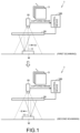
- FIG. 1 is a diagram schematically showing an image inspection apparatus 1 according to the present embodiment.
- the image inspection apparatus 1 is applied to an apparatus which captures an image of an object (hereinafter referred to as a "workpiece W") while illuminating the object and inspects the exterior (for scratches, contamination, foreign materials and the like) of the workpiece W using the acquired captured image in a production line for industrial products, and the like.
- the image inspection apparatus 1 inspects a workpiece W by detecting light reflected by the workpiece W. Accordingly, a workpiece having a surface which reflects light is applicable to the workpiece W.
- a workpiece W has a surface which diffuses and reflects light.
- a material which diffuses and reflects light may be a resin or a metal, for example. Meanwhile, it is not necessary to limit the workpiece W such that the entire surface thereof diffuses and reflects light. Only a part to which light is radiated may diffuse and reflect the light. Further, if the present embodiment is applicable, the material of the workpiece W need not be limited to a resin or a metal.
- the image inspection apparatus 1 includes a camera 10 which is an example of an image capturing unit, an illumination device 20 which is an example of an illumination unit, and a control device 100 which is an example of a control unit configured to control the camera 10 and the illumination device 20.
- the camera 10 captures an image of a workpiece W which is an object to generate a captured image of the workpiece W.
- the illumination device 20 is disposed between the camera 10 and the workpiece W and has a light-emitting surface which radiates light to the workpiece W.
- the illumination device 20 is configured to be able to control a light-emitting position on the light-emitting surface and a radiation direction of light.
- the illumination device 20 has translucency.
- the camera 10 captures an image of the workpiece W over the illumination device 20. It is desirable that the illumination device 20 have a degree of translucency at which the camera 10 can capture an image of the workpiece W through the illumination device 20.
- the illumination device 20 can change a radiation direction of light and an illumination pattern according to an instruction from the control device 100.
- the illumination device 20 radiates light such that the light is caused to scan on the surface of the workpiece W according to an instruction from the control device 100.
- the camera 10 captures images of the workpiece W to acquire a plurality of captured images.
- the control device 100 causes the illumination device 20 to radiate light to the workpiece W in a first direction in first scanning of the illumination device 20.
- the control device 100 causes light to be scanned by changing a light-emitting position in the light-emitting surface of the illumination device 20.
- the illumination device 20 radiates light to the workpiece W in a direction that forms a predetermined angle with the optical axis 11 (optical center) of the camera 10 and causes the light to scan in a +X direction in the first scanning.
- the control device 100 causes the camera 10 to capture images of the workpiece W multiple times. Accordingly, the camera 10 generates a plurality of captured images 3.
- the control device 100 causes the illumination device 20 to radiate light to the workpiece W in a direction different from the radiation direction in the first scanning. Further, the control device 100 causes light to be scanned by changing the light-emitting position on the light-emitting surface of the illumination device 20. For example, the illumination device 20 radiates light to the workpiece W in a direction reverse to the radiation direction in the first scanning and causes the light to scan in a -X direction in the second scanning.
- the control device 100 causes the camera 10 to capture images of the workpiece W multiple times as in the first scanning. Accordingly, the camera 10 generates a plurality of captured images 5.
- the control device 100 identifies a light-emitting position of the illumination device 20 when a measurement point of the surface of the workpiece W is illuminated from the images (the plurality of captured images 3 and the plurality of captured images 5) of the workpiece W captured in the first scanning and the second scanning.
- a "measurement point" is a position on the surface of the workpiece W at which a distance from the light-emitting surface will be measured.
- the control device 100 calculates a distance between the light-emitting surface of the illumination device 20 and the measurement point on the basis of the identified light-emitting position, the light radiation direction (first direction) in the first scanning and the light radiation direction (second direction) in the second scanning.
- FIG. 2 is a schematic diagram for describing a process performed by the control device shown in FIG. 1 .
- the control device 100 generates a processing image from a plurality of captured images.
- the plurality of captured images have a plurality of pixels disposed in 2 dimensions. Accordingly, the same number of pixels as the number of captured images is acquired at each pixel position.
- the control device 100 selects one pixel from such a plurality of pixels to generate a processing image.
- a processing image 4 having information about a first light-emitting position which is a light-emitting position for illuminating the measurement point of the workpiece W is generated from the plurality of captured images 3.
- a pixel PX1 positioned at a pixel position (x, y) is a pixel selected from pixels at the same pixel position (x, y) of the plurality of captured images 3.
- the pixel PX1 has information about the first light-emitting position as a pixel value.
- a processing image 6 having information about a second light-emitting position which is a light-emitting position for illuminating the measurement point of the workpiece W is generated from the plurality of captured images 5.
- a pixel PX2 positioned at a pixel position (x, y) is a pixel selected from pixels at the same pixel position (x, y) of the plurality of captured images 5.
- the pixel PX2 has information about the second light-emitting position as a pixel value.
- the position (x, y) of the pixel PX2 within the processing image 6 is the same as the pixel position (x, y) in the pixel PX1 within the processing image 4.
- the control device 100 calculates a distance between the illumination device 20 and the workpiece W for each pixel on the basis of the processing images 4 and 6. Specifically, the control device 100 calculates a distance between the light-emitting surface of the illumination device 20 and the position of the surface (measurement point) of the workpiece W on the basis of information on the first light-emitting position included in the pixel PX1 of the processing image 4, information on the second light-emitting position included in the pixel PX2 of the processing image 6, and the light radiation directions (the first direction and the second direction) in the first scanning and the second scanning. The control device 100 generates a distance image 7 including a pixel PX having the calculated distance as a pixel value.
- the information included in the pixel PX1 of the processing image 4 and the information included in the pixel PX2 at the same position as the pixel PX1 in the processing image 6 are used in order to calculate the distance between the illumination device 20 and the surface of the workpiece W.
- the radiation direction of light emitted from the illumination device 20 and the light-emitting position in the illumination device 20 are controllable. Accordingly, the control device 100 can have information about the light-emitting position and the radiation direction.
- the position of the camera 10 with respect to the illumination device 20 is not particularly limited. That is, is it not necessary to dispose the illumination device at a specific position with respect to the optical axis of the image capturing unit. Accordingly, it is possible to provide an image inspection apparatus and an image inspection method capable of inspecting an object without a necessity for calibration between the imaging capturing unit and the illumination device.
- FIG. 3 is a schematic diagram showing an example of a production line to which the image inspection apparatus 1 according to the present embodiment is applied.
- the image inspection apparatus 1 captures images of a workpiece W using the camera 10 while illuminating the workpiece W through the illumination device 20 and inspects the exterior of the workpiece W using the acquired captured images in a production line for industrial products, and the like.
- the workpiece W which is an inspection target is moved by a movable stage 300 to an inspection position at which the camera 10 and the illumination device 20 are fixed.
- the workpiece W remains still in that place until exterior inspection performed by the image inspection apparatus 1 ends.
- control device 100 captures images of the workpiece W using the camera 10 while illuminating the workpiece W through the illumination device 20 and displays the captured images on a monitor. Accordingly, an operator inspects the exterior of the workpiece W while viewing the colors of the captured images displayed on a monitor screen.
- control device 100 may perform predetermined image processing on the captured images and perform abnormality determination with respect to the workpiece W on the basis of an image processing result.
- control device 100 may include a processor such as a central processing unit (CPU) or a micro-processing unit (MPU), a random access memory (RAM), a display controller, a system controller, an input/output (I/O) controller, a hard disk, a camera interface, an input interface, a light emission interface, a communication interface, and a memory card interface.
- a processor such as a central processing unit (CPU) or a micro-processing unit (MPU), a random access memory (RAM), a display controller, a system controller, an input/output (I/O) controller, a hard disk, a camera interface, an input interface, a light emission interface, a communication interface, and a memory card interface.
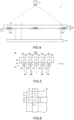
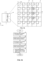
- FIG. 4 is a diagram schematically showing a configuration of the illumination device included in the image inspection apparatus 1.
- the illumination device 20 is disposed between a workpiece W and the camera 10, radiates light to the workpiece W and has translucency. Accordingly, light radiated from the illumination device 20 is reflected by the workpiece W, is transmitted by the illumination device 20 and arrives at the camera 10.
- the illumination device 20 includes a surface light source 30 and a micro-lens array 40 which is an example of an optical system.
- the surface light source 30 radiates light to the workpiece W from a light-emitting surface 35 at the side of the workpiece W. Light is radiated from a plurality of light-emitting regions arranged in a matrix form on the light-emitting surface 35 of the surface light source 30. Reflected light from the workpiece W is transmitted by a light-transmitting region other than the light-emitting regions in the surface light source 30.
- Each light-emitting region includes a light-emitting unit 31.
- the light-emitting unit 31 includes a member configured according to organic electroluminescence (hereinafter referred to as organic EL).
- organic EL organic electroluminescence
- a plurality of light-emitting units 31 are configured to be able to selectively emit light.
- a light-emitting unit 31 to emit light is selected by the control device 100 (refer to FIG. 1 ).
- the surface light source 30 is a light source using organic EL.
- any illumination device having translucency and a plurality of light-emitting units arranged in a matrix form and configured to selectively emit light is applicable to the present embodiment. That is, the illumination device 20 applicable to the present embodiment is not limited to a light source using organic EL.
- the micro-lens array 40 is disposed to face the light-emitting surface 35 of the surface light source 30.
- the micro-lens array 40 includes a plurality of lenses 41 provided to face the plurality of light-emitting units 31.
- the lenses 41 are convex lenses.
- the lenses 41 are configured to guide light emitted from the light-emitting units 31 corresponding thereto in a desired direction. That is, the micro-lens array 40 is configured to control a radiation direction of light emitted from each of the plurality of light-emitting units 31 to be a direction corresponding to the position of each light-emitting unit 31.
- a radiation solid angle may be arbitrarily changed by selecting a light-emitting unit to emit light from the plurality of light-emitting units 31.
- a light-emitting unit to emit light is selected according to a place of a visual field. Accordingly, it is possible to realize the image inspection apparatus 1 capable of arbitrarily setting a radiation solid angle for each place of a visual field. Further, since the radiation solid angle can be arbitrarily changed, an optical part such as a slit or a half mirror, for example, can be unnecessary. Accordingly, the illumination device 20 can be reduced in size. Therefore, it is possible to realize the image inspection apparatus 1 which can set a radiation solid angle for each place of a visual field and can be reduced in size.
- FIG. 5 is a schematic diagram showing a cross section of a part of an example of the illumination device according to the present embodiment.
- FIG. 6 is an enlarged schematic plan view of a part of the illumination device according to the present embodiment.
- the illumination device 20 is a transmission type sheet illumination device and includes the surface light source 30 and the micro-lens array 40.
- the surface light source 30 is a light source using organic EL.
- the surface light source 30 includes a plurality of light-emitting units arranged in a matrix form along the light-emitting surface 35.
- FIG. 5 representatively shows light-emitting units 31A to 31E.
- Each of the light-emitting units 31A to 31E has a pair of electrodes (not shown) facing each other. When a voltage is applied across the pair of electrodes, the light-emitting unit emits light.
- a light-emitting unit to emit light may be selected by selecting an electrode pair to which a voltage will be applied from a plurality of electrode pairs.
- the color of light emitted from each of the light-emitting units 31A to 31E is not limited.
- the plurality of light-emitting units 31 may emit light in the same color.
- light-emitting units capable of emitting light in different colors may be realized by combining a light-emitting unit which emits red light, a light-emitting unit which emits green light and a light-emitting unit which emits blue light.
- the micro-lens array 40 includes a plurality of lenses 41 which are a plurality of micro-lenses arranged to face the plurality of light-emitting units 31.
- the plurality of lenses 41 are arranged in a matrix form along the light-emitting surface 35.
- FIG. 5 representatively shows lenses 41A to 41E facing the light-emitting units 31A to 31E.
- the lenses 41A to 41E are planoconvex lenses.
- the surfaces of the planoconvex lenses face the light-emitting surface 35.
- the planoconvex lenses may be hemispherical lenses.
- Each lens is for controlling a radiation direction of light emitted from the corresponding light-emitting unit.
- relative positions of the optical axes of the lenses with respect to the optical axes of light-emitting units are different.
- the direction of light emitted from a lens is determined according to a direction of deviation of the optical axis of the lens with respect to the optical axis of the corresponding light-emitting unit and a deviation amount.
- the optical axis of a light-emitting unit refers to an axis which penetrates the center point of a light-emitting region and is perpendicular to the light-emitting region and the optical axis of a lens refers to an axis which penetrates the center of the lens and is perpendicular to the principal plane of the lens.
- “Deviation amount” refers to a magnitude of deviation of the optical axis of a lens with respect to the optical axis of a light-emitting unit.
- the optical axis 32C of the light-emitting unit 31C and the optical axis 42C of the lens 41C are substantially consistent with each other.
- the optical axis 42A of the lens 41A deviates from the optical axis 32A of the light-emitting unit 31A to the right on the paper (in the +X direction).
- the optical axis 42B of the lens 41B also deviates from the optical axis 32B of the light-emitting unit 31B in the +X direction.
- a deviation amount with respect to the pair of the light-emitting unit 31A and the lens 41A is greater than that with respect to the pair of the light-emitting unit 31B and the lens 41B.
- the optical axis 42D of the lens 41D deviates from the optical axis 32D of the light-emitting unit 31D to the left on the paper (in the -X direction).
- the optical axis 42E of the lens 41E also deviates from the optical axis 32E of the light-emitting unit 31E in the -X direction.
- a deviation amount with respect to the pair of the light-emitting unit 31E and the lens 41E is greater than that with respect to the pair of the light-emitting unit 31D and the lens 41D.
- the illumination device 20 includes a plurality of illumination elements 21 arranged in a matrix form. That is, the illumination device 20 is sectioned into the plurality of illumination elements 21.
- Each illumination element 21 includes a plurality of light-emitting units 31 and a plurality of lenses 41.
- each illumination element 21 may include the light-emitting units 31A to 31E and the lenses 41A to 41E shown in FIG. 5.
- FIG. 6 shows a single light-emitting unit 31 and a single lens 41 corresponding thereto included in each illumination element 21 for illustration.
- Each illumination element 21 includes a light-emitting region and a transparent region. It is possible to cause the entire illumination element 21 to emit light by causing the transparent region to emit light. Meanwhile, each illumination element 21 has translucency by including the transparent region.
- the illumination device 20 may independently turn on the plurality of illumination elements 21.
- An illumination pattern of the illumination device 20 is determined by illumination elements 21 including light-emitting units 31 to emit light (i.e., illumination elements 21 to be turned on) among the plurality of illumination elements 21.
- an illumination pattern may be determined by illumination elements 21 which are turned on among the plurality of illumination elements 21 and the wavelength of light radiated from each illumination element 21 which is turned on.
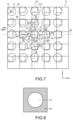
- FIG. 7 is a plan view schematically showing an example of a structure of an illumination element which is a component of the illumination device 20.
- FIG. 7 shows a planar view of the illumination element at the side of the image capturing unit (above the illumination device 20).
- the illumination element 21 includes a plurality of cells 22 arranged in a matrix form.
- “row” refers to an X direction and “column” refers to a Y direction.
- the number of cells constituting the illumination element 21 is not particularly limited.
- the number of cells 22 constituting the illumination element 21 can be determined by the resolution of a radiation direction and the resolution of a light-emitting position.
- Each cell 22 includes a light-emitting unit 31, a lens 41 and a transparent region 24.
- a light-emitting surface of the light-emitting unit 31 constitutes a light-emitting region in the cell 22.
- a plurality of light-emitting units 31 are arranged at a first pitch P1 in the X direction and the Y direction.
- a plurality of lenses 41 are arranged at a second pitch P2 in the X direction and the Y direction. Since the second pitch P2 is less than the first pitch P1 (P2 ⁇ P1), a deviation amount in the X direction between the optical axis 32 of the light-emitting unit 31 and the optical axis 42 of the lens 41 conforms to an arithmetic progression of a tolerance (P1-P2) with respect to a plurality of cells 22 aligned in the X direction (row direction).
- a deviation amount in the Y direction between the optical axis 32 of the light-emitting unit 31 and the optical axis 42 of the lens 41 conforms to the arithmetic progression of the tolerance (P1-P2) with respect to a plurality of cells 22 aligned in the Y direction (column direction).
- the plurality of light-emitting units 31 and the plurality of lenses 41 are arranged symmetrically with respect to both the X axis and the Y axis.
- axes 25 and 26 of symmetry are shown in FIG. 7 .
- the axis 25 of symmetry is an axis for representing that the plurality of light-emitting units 31 and the plurality of lenses 41 are arranged symmetrically with respect to the X axis and is parallel with the Y direction.
- the axis 26 of symmetry is an axis for representing that the plurality of light-emitting units 31 and the plurality of lenses 41 are arranged symmetrically with respect to the Y axis and is parallel with the X direction.
- a cell 22C is a cell positioned at the center of the illumination element 21.
- the cell 22C includes a light-emitting unit 31C and a lens 41C.
- the optical axis 32C of the light-emitting unit 31C and the optical axis 42C of the lens 41C overlap in the planar view. That is, both a deviation amount in the X direction and a deviation amount in the Y direction are 0 between the optical axis 32C and the optical axis 42C. Meanwhile, the optical axes 32C and 42C are positioned at the intersection of the axes 25 and 26 of symmetry.
- a deviation amount in the X direction and a deviation amount in the Y direction between the optical axis 32 of the light-emitting unit 31 and the optical axis 42 of the lens 41 are determined according to a distance in the X direction and a distance in the Y direction between the cell and the central cell 22C. Accordingly, it is possible to make a radiation direction of light different for the respective cells 22.
- the illumination element 21 may radiate light to a workpiece in a plurality of directions. Further, a radiation direction of light from the illumination element 21 may be controlled by selecting a cell to be turned on from the plurality of cells.
- the pitch of the light-emitting units 31 is the same as the pitch of the lenses 41 in the X direction and the Y direction. However, the pitch of the light-emitting units 31 may be different in the X direction and the Y direction. Similarly, the pitch of the lenses 41 may be different in the X direction and the Y direction.
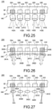
- FIG. 8 is a schematic plan view showing a configuration for a countermeasure against light leaking from the edge of the lens 41.
- FIG. 9 is a schematic cross-sectional view of the configuration shown in FIG. 8 .
- a light-shielding part 44 may be provided to surround the edge of the lens 41.
- the light-shielding part 44 is formed of a material which does not pass light or a material which attenuates light. The possibility of light from the light-emitting unit 31 leaking in an unintended direction can be reduced according to the light-shielding part 44.
- FIG. 10 is a schematic plan view showing a modified example of the configuration shown in FIG. 8 .
- the area of the light-shielding part 44 is larger than that in the configuration shown in FIG. 8 . Accordingly, the possibility of light from the light-emitting unit 31 leaking in an unintended direction can be further reduced.
- FIG. 11 is a schematic cross-sectional view showing another modified example of the configuration shown in FIG. 8 .
- the light-shielding part 44 has a configuration of surrounding the edge of the lens 41 with a sufficient height in the direction of the height (thickness) of the lens 41 in addition to the configuration shown in FIG. 10 .
- the effect of reducing light leaking from the edge of the lens 41 can be further improved.
- the surface of a workpiece is inspected using a light sectioning method.
- the illumination device 20 radiates light in a line form to a workpiece W in a certain direction and causes the light to scan.
- the camera 10 captures images of the workpiece W multiple times while the light is caused to scan to generate a plurality of captured images. As described above, light scanning is performed twice.
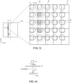
- FIG. 12 is a diagram for describing first scanning of light when the light sectioning method is performed.
- FIG. 13 is a diagram for describing an illumination pattern of the illumination device for radiation light shown in FIG. 12 .
- the configuration of the illumination element 21 shown in FIG. 13 and figures which will be described below is basically the same as the configuration shown in FIG. 5 , and thus detailed description thereof will not be repeated. Meanwhile, in the figures which will be described below, a region emitting light in the illumination device 20 and a light-emitting unit emitting light in an illumination element are represented by hatching.
- the illumination device 20 radiates light LT in a line form to a workpiece W in a direction that forms an angle ⁇ with respect to the optical axis 11 of the camera 10 and causes the light LT to scan in the +X direction. While the light LT scans, the camera 10 captures images of the surface of the workpiece W multiple times. Accordingly, a plurality of captured images are acquired.
- FIG. 13 shows a state of the illumination device 20 during scanning of light.
- a straight line L1 shown in FIG. 13 is a virtual straight light for representing X coordinates of the optical axis of the camera 10 and is a straight line parallel with the Y axis.
- the illumination device 20 turns on a plurality of illumination elements 21 aligned in the Y direction.
- FIG. 13 shows a state in which a plurality of illumination elements 21 positioned in the -X direction and separated from the straight line L1 by a distance d1 are turned on.
- three light-emitting units 31 arranged in a specific column e.g., column C2
- the illumination device 20 is able to radiate light in a line form in the Y direction to a desired place of the surface of the workpiece W in a direction at an angle ⁇ to the optical axis 11 of the camera 10.
- FIG. 14 is a diagram for describing second scanning of light when the light sectioning method is performed.
- FIG. 15 is a diagram for describing an illumination pattern of the illumination device for radiation of light shown in FIG. 14 .
- the illumination device 20 radiates the light LT in a line form to the workpiece W in a reverse direction of the light radiation direction in the first scanning.
- the direction in which the light is radiated is at an angle ⁇ to the optical axis 11 of the camera 10.
- the illumination device 20 causes the light LT to scan in the -X direction, for example. However, the illumination device 20 may cause the light LT to scan in the +X direction as in the first scanning. While the light LT scans, the camera 10 captures images of the surface of the workpiece W. Accordingly, a plurality of captured images are acquired.
- FIG. 15 shows a state in which a plurality of illumination elements 21 positioned in the +X direction and separated from the straight line L1 by a distance d2 are turned on.
- three light-emitting units 31 arranged in a specific column e.g., column C4 emit light.
- the light-emitting units 31 and the lenses 41 are arranged symmetrically with respect to the axis 25 of symmetry when the column C2 and the column C4 are compared with each other.
- the illumination device 20 is able to radiate light in a line form in the Y direction to a desired place of the surface of the workpiece W in a direction which is reverse to the light radiation direction in the first scanning and forms the angle ⁇ to the optical axis 11 of the camera 10.
- FIG. 16 is a flowchart showing a distance calculation method included in an inspection method according to embodiment 1.
- the distance calculation method according to embodiment 1 will be described below with reference to FIGS. 2 and 16 .
- the illumination device 20 performs first scanning of light and the camera 10 captures images of a workpiece W n times (n is an integer equal to or greater than 2). Accordingly, n images (n captured images 3) are acquired.
- step S2 the control device 100 generates the processing image 4 from the n images acquired through the process of step S1. Specifically, the control device 100 identifies a pixel having a maximum luminance from the n captured images for each pixel position (x, y). In addition, the control device 100 includes a distance d1 (refer to FIGS. 12 and 13 ) when the images are acquired in information on the pixel.
- the distance d1 represents a first light-emitting position of the illumination device 20 when the luminance of a pixel (pixel at the pixel position (x, y)) corresponding to a measurement point on the surface of the workpiece W is maximized.
- Each pixel in the processing image 4 has information on the distance d1 which gives a highest luminance value as a pixel value. Meanwhile, the processing image 4 is referred to as "d1 image" in FIG. 16 .
- step S3 the illumination device 20 performs second scanning of light and the camera 10 captures images of the workpiece W n times. Accordingly n images are acquired.
- step S4 the control device 100 generates the processing image 6 from the n images (n captured images 5) acquired through the process of step S3.
- step S4 the control device 100 generates the processing image 6 from the n images (n captured images 5) acquired through the process of step S3.
- the control device 100 identifies a pixel having a maximum luminance from the n captured images for each pixel position (x, y).
- the control device 100 includes a distance d2 (refer to FIGS. 14 and 15 ) when the images are acquired in pixel information.
- the distance d2 represents a second light-emitting position of the illumination device 20 when the luminance of the pixel (pixel at the pixel position (x, y)) corresponding to the measurement point on the surface of the workpiece W is maximized.
- Each pixel in the processing image 6 has information on the distance d2 which gives a highest luminance value as a pixel value. Meanwhile, the processing image 6 is referred to as "d2 image" in FIG. 16 .
- step S5 the control device 100 calculates a distance D corresponding to a pixel of each coordinates (x, y) using the d1 image (processing image 4) and the d2 image (processing image 6).
- the distance D is a distance between the light-emitting surface 35 of the illumination device 20 and the measurement point on the surface of the workpiece W corresponding to the pixel of the coordinates (x, y).
- FIG. 17 is a diagram describing the principle of the distance calculation method according to embodiment 1.
- a measurement point 13 corresponds to a position on the surface of the workpiece W corresponding to the pixel of the coordinates (x, y).
- the pixel PX1 in the processing image 4 (d1 image) and the pixel PX2 in the processing image 6 (d2 image) are pixels corresponding to the measurement point 13.
- a straight line 12 penetrates the measurement point 13 and is parallel with a central line 28 (a straight line which penetrates the center of the light-emitting surface 35 and is perpendicular to the light-emitting surface 35) of the illumination device 20.
- a distance between the central line 28 of the illumination device 20 and the straight line 12 is set to d
- the following equations (1) and (2) are established.
- d D ⁇ tan ⁇
- D d 1 + d 2 / 2 ⁇ tan ⁇ ⁇ is an emission direction of light from the illumination device 20.
- the control device 100 controls a direction in which light is emitted from the illumination device 20 by controlling the illumination device 20. Accordingly, the control device 100 can be aware of the value of the angle ⁇ .
- the distances d1 and d2 are information included in the pixels of the processing image 4 and the pixels of the processing image 6 and are determined according to conditions of scanning of light performed by the illumination device 20.
- the equation (4) does not include the distance d, the equation (4) is established with respect to an arbitrary position on the surface of the workpiece W. It is possible to calculate the distance D between the light-emitting surface 35 of the illumination device 20 and an arbitrary position on the surface of the workpiece W on the basis of the distance d1 (first light-emitting position), the distance d2 (second light-emitting position) and the angle ⁇ (radiation direction of light) by using the equation (4).
- the distances d1 and d2 are distances from the center of the light-emitting surface 35. Since the plurality of illumination elements 21 are arranged in a matrix form, the distances d1 and d2 can be determined. Accordingly, it is possible to perform inspection of an object without a necessity for calibration between the image capturing unit and the illumination device.
- a range of one edge to the other edge of a light-emitting region in the light-emitting surface may be scanned (whole scanning).
- the scanning range may be limited.
- the value of the angle ⁇ which determines a radiation direction of light may be varied according to the shape of a workpiece W. A plurality of trials may be performed while changing the value of the angle ⁇ and results may be integrated.
- the scanning direction is the X direction in the above description
- scanning in the Y direction may be performed.
- the X direction (X axis) may be substituted by the Y direction (Y axis) and the axis 25 of symmetry may be substituted by the axis 26 of symmetry.
- Measurement according to scanning in the X direction and measurement according to scanning in the Y direction may be tried and results thereof may be integrated.
- three of the five light-emitting units 31 included in one column of the illumination element 21 are turned on in the above-described description. However, all of the (5) light-emitting units 31 included in one column may be caused to emit light. Alternatively, only one light-emitting unit 31 positioned at the center of one column may be caused to emit light.
- the surface of a workpiece is inspected using a phase shift method.
- the illumination device 20 radiates light in a striped pattern to a workpiece W in a certain direction and causes the light to scan.
- the camera 10 captures images of the workpiece W multiple times while the light is caused to scan to generate a plurality of captured images. As in embodiment 1, light scanning is performed twice.
- FIG. 18 is a diagram for describing first scanning of light when the phase shift method is performed.
- FIG. 19 is a diagram for describing an illumination pattern of the illumination device for radiation of light shown in FIG. 18 .
- the illumination device 20 radiates light LT to a workpiece W in a direction that forms an angle ⁇ with respect to the optical axis 11 of the camera 10.
- the camera 10 captures images of the surface of the workpiece W.
- the illumination device 20 radiates a light in a striped pattern (light-and-shade pattern) to the workpiece W while changing the phase of the striped pattern. Accordingly, a state equivalent to scanning of light in a striped pattern on the surface of the workpiece W may be generated. Since the illumination pattern is a periodic pattern, the illumination device 20 may change the phase by one period. In the example shown in FIG. 18 , the illumination pattern is scanned in the +X direction.
- the illumination device 20 turns on illumination elements 21 in a plurality of columns such that light and shade are alternately generated in the X direction.
- L represents a length corresponding to the period of the striped pattern.
- the illumination device 20 may be controlled such that the intensity of light emission changes according to a sine wave.
- three light-emitting units 31 arranged in a specific column e.g., column C2 emit light in each of the plurality of illumination elements 21.
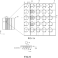
- FIG. 20 is a diagram for describing second scanning of light when the phase shift method is performed.
- FIG. 21 is a diagram for describing an illumination pattern of the illumination device for radiation of light shown in FIG. 20 .
- the illumination device 20 radiates light LT to the workpiece W in a direction reverse to the radiation direction of light in the first scanning.
- a direction in which light is radiated forms an angle ⁇ to the optical axis of the camera 10.
- the illumination device 20 causes the light LT to scan in the -X direction, for example. However, the illumination device 20 may cause the light LT to scan in the +X direction as in the first scanning.
- the camera 10 captures images of the surface of the workpiece W multiple times while the light LT is caused to scan.
- three light-emitting units 31 arranged in a specific column emit light in each of the plurality of illumination elements 21.
- the illumination device 20 can radiate light in a direction which is reverse to the radiation direction of light in the first scanning and forms the angle ⁇ to the optical axis 11 of the camera 10.
- FIG. 22 is a flowchart showing a distance calculation method included in an inspection method according to embodiment 2.
- the distance calculation method according to embodiment 2 will be described below with reference to FIGS. 2 and 22 .
- the illumination device 20 performs first scanning of light. That is, the illumination device 20 changes the phase of an illumination pattern by one period, for example. A change amount of the phase is not particularly limited.
- the camera 10 captures images of the workpiece W n times (n is an integer equal to or greater than 2). Accordingly, n images are acquired.
- step S12 the control device 100 generates the processing image 4 having a phase ⁇ of the illumination pattern (striped pattern) as a pixel value from the n images (n captured images 3) acquired through the process of step S11.
- phase image 1 For example, it is assumed that light is emitted according to a sine-wave pattern in the light-emitting surface (light-emitting surface 35) of the illumination device 20.
- a maximum point of a sine wave represents a maximum value of illumination intensity
- a minimum point of the sine wave represents a minimum value of illumination intensity
- an intermediate point between the maximum point and the minimum point of the sine wave represents an intermediate value of illumination intensity.
- the processing image 4 is referred to as "phase image 1" in FIG. 22 .
- FIG. 23 is a schematic diagram for describing a method of obtaining a phase of an illumination pattern.
- a certain point A1 on the light-emitting surface 35 is correlated with a point B1 on the surface of a workpiece W.
- images of the surface of the workpiece W is captured using the camera 10 while changing the phase of a light emission pattern by 90° and luminance values (concentration values) of pixels may be recorded.
- luminance values concentration values
- the fitted sine wave is represented as sin(x-a) when a reference wave is sin(x).
- the value a is a phase. That is, the method of obtaining a phase of an illumination pattern is a method of obtaining a phase difference from the reference wave. With respect to a point B2 on the surface of the workpiece W, a phase is also obtained through the same method.
- a luminance value has an error. Accordingly, the number of points representing a luminance value increases as a phase change decreases, and thus a phase with higher accuracy can be obtained.
- the illumination device 20 performs second scanning of light and the camera 10 captures images of the workpiece W n times in step S13. Accordingly, n images are acquired.
- the control device 100 generates the processing image 6 having a phase ⁇ of the illumination pattern as a pixel value from the n images (n captured images 5) obtained through the process of step S13.
- the process of step S13 is the same as the process of step S12 (refer to FIG. 23 ). Meanwhile, the processing image 6 is referred to as "phase image 2" in FIG. 22 .
- step S15 the control device 100 calculates a distance D corresponding to a pixel of each coordinates (x,y) using phase image 1 (processing image 4) and phase image 2(processing image 6).
- FIG. 24 is a diagram describing the principle of the distance calculation method according to embodiment 2.
- the equation (4) is also established.
- Distances d1 and d2 are represented according to the following equations (5) and (6).
- the phases ⁇ and ⁇ are pixel values (phase values) included in pixels of the processing image 4 and pixels of the processing image 6. Accordingly, it is possible to calculate the distance D by putting the equations (5) and (6) into the equation 4.
- a relative distance from a virtual plane 50 parallel with the light-emitting surface 35 can be calculated through the phase shift method.
- the distance D is the relative distance.
- FIG. 24 shows a single virtual plane (virtual plane 50), a plurality of candidates at specific intervals and in parallel with the light-emitting surface 35 may be present as virtual planes.
- FIG. 25 is a schematic diagram showing a cross section of a part of an illumination device 120 according to modified example 1.
- the illumination device 120 includes a micro-lens array 140 instead of the micro-lens array 40.
- the micro-lens array 140 includes a plurality of lenses 141 which are a plurality of micro-lenses disposed to face a plurality of light-emitting units 31.
- FIG. 25 representatively shows lenses 141A to 141E facing light-emitting units 31A to 31E.
- Each of the lenses 141A to 141E is a rod lens.
- angles of the optical axes (optical axes 142A to 142E) of the lenses to the optical axes (optical axes 32A to 32E) of the light-emitting units 31 are different. It is possible to change emission angles (angles to the optical axes of the lenses) of light emitted from emission surfaces of the rod lenses by changing incident angles of light to incident surfaces of the rod lenses. Accordingly, an emission direction of light can be changed for each light-emitting unit in the illumination device 120. It is possible to increase a distance between a workpiece W and the illumination device 120, in which the shape of the workpiece W can be inspected by using rod lenses.
- FIG. 26 is a schematic diagram showing a cross section of a part of an illumination device 220 according to modified example 2.
- the illumination device 220 includes a micro-lens array 240 instead of the micro-lens array 40.
- the micro-lens array 240 includes a plurality of lenses 241 which are a plurality of micro-lenses disposed to face a plurality of light-emitting units 31.
- FIG. 26 representatively shows lenses 241A to 241E facing light-emitting units 31A to 31E.
- Each of the lenses 241A to 241E is a concave lens.
- angles of the optical axes of the lenses to the optical axes of the light-emitting units 31 are different. It is possible to change emission angles (angles to the optical axes of the lenses) of light emitted from the concave lenses by changing angles of the optical axes (optical axes 242A to 242E) of the lenses to the optical axes (optical axes 32A to 32E) of the light-emitting units.
- FIG. 27 is a schematic diagram showing a cross section of a part of an illumination device 320 according to modified example 3.
- the illumination device 320 includes a micro-lens array 340 instead of the micro-lens array 40.
- the micro-lens array 340 includes a plurality of lenses 341 which are a plurality of micro-lenses disposed to face a plurality of light-emitting units 31.
- FIG. 27 representatively shows lenses 341A to 341E facing light-emitting units 31A to 31E.
- the lenses 41A to 41E in the configuration of FIG. 3 are substituted by the lenses 341A to 341E and the optical axes 42A to 42E are substituted by optical axes 342A to 342E.
- Each of the lenses 341A to 341E is a convex lens.
- the shape of each of the lenses 341A to 341E differs from the shapes of the lenses 41A to 41E. As in the example shown in FIG.
- illumination elements include a plurality of cells 22 arranged in a matrix form. It is possible to change inclination angles of the optical axes of the lenses to the optical axes of the light-emitting units according to positions of the cells in the plurality of cells 22. Further, the angle of the optical axis of a lens to the X axis and the angle of the optical axis of a lens to the Y axis may be different for each cell.
- the light-shielding part 44 (refer to FIGS. 8 to 11 ) may be provided at the edges of the lenses in the micro-lens arrays 140, 240 and 340 shown in FIGS. 25 to 27 .
Landscapes
- Physics & Mathematics (AREA)
- General Physics & Mathematics (AREA)
- General Health & Medical Sciences (AREA)
- Chemical & Material Sciences (AREA)
- Analytical Chemistry (AREA)
- Biochemistry (AREA)
- Life Sciences & Earth Sciences (AREA)
- Health & Medical Sciences (AREA)
- Immunology (AREA)
- Pathology (AREA)
- Engineering & Computer Science (AREA)
- Computer Vision & Pattern Recognition (AREA)
- Signal Processing (AREA)
- Investigating Materials By The Use Of Optical Means Adapted For Particular Applications (AREA)
- Length Measuring Devices By Optical Means (AREA)
Applications Claiming Priority (1)
| Application Number | Priority Date | Filing Date | Title |
|---|---|---|---|
| JP2018030930A JP6939640B2 (ja) | 2018-02-23 | 2018-02-23 | 画像検査装置および画像検査方法 |
Publications (2)
| Publication Number | Publication Date |
|---|---|
| EP3531115A1 EP3531115A1 (en) | 2019-08-28 |
| EP3531115B1 true EP3531115B1 (en) | 2023-07-05 |
Family
ID=65030993
Family Applications (1)
| Application Number | Title | Priority Date | Filing Date |
|---|---|---|---|
| EP19151856.2A Active EP3531115B1 (en) | 2018-02-23 | 2019-01-15 | Image inspection apparatus and image inspection method |
Country Status (4)
| Country | Link |
|---|---|
| US (1) | US11536667B2 (enExample) |
| EP (1) | EP3531115B1 (enExample) |
| JP (2) | JP6939640B2 (enExample) |
| CN (1) | CN110186927B (enExample) |
Families Citing this family (3)
| Publication number | Priority date | Publication date | Assignee | Title |
|---|---|---|---|---|
| JP7665291B2 (ja) * | 2020-03-30 | 2025-04-21 | 株式会社島津製作所 | 走査型プローブ顕微鏡および走査型プローブ顕微鏡における光軸調整方法 |
| JP7392582B2 (ja) * | 2020-06-12 | 2023-12-06 | オムロン株式会社 | 検査システムおよび検査方法 |
| CN115790402B (zh) * | 2022-10-25 | 2023-07-21 | 北京泊菲莱科技有限公司 | 一种球型光源尺寸测量方法及装置 |
Family Cites Families (16)
| Publication number | Priority date | Publication date | Assignee | Title |
|---|---|---|---|---|
| US6618123B2 (en) * | 2000-10-20 | 2003-09-09 | Matsushita Electric Industrial Co., Ltd. | Range-finder, three-dimensional measuring method and light source apparatus |
| US7193697B2 (en) * | 2005-07-25 | 2007-03-20 | Chroma Ate Inc. | Apparatus for feature detection |
| WO2007026690A1 (ja) * | 2005-08-31 | 2007-03-08 | Ccs Inc. | 同軸光照射装置 |
| JP2008185380A (ja) * | 2007-01-29 | 2008-08-14 | Nikon Corp | 形状測定装置 |
| JP2009164033A (ja) * | 2008-01-09 | 2009-07-23 | Konica Minolta Holdings Inc | 有機エレクトロルミネッセンス素子の製造方法、有機エレクトロルミネッセンス素子、表示装置及び照明装置 |
| JP5055191B2 (ja) * | 2008-04-24 | 2012-10-24 | パナソニック株式会社 | 3次元形状計測方法および装置 |
| JP2014096253A (ja) * | 2012-11-08 | 2014-05-22 | Yamagata Prefecture | 透視性を有する面状光源及びそれを用いた撮像方法 |
| US20150015701A1 (en) * | 2013-07-10 | 2015-01-15 | Faro Technologies, Inc. | Triangulation scanner having motorized elements |
| DE102013111761B4 (de) * | 2013-10-25 | 2018-02-15 | Gerhard Schubert Gmbh | Verfahren und Scanner zum berührungslosen Ermitteln der Position und dreidimensionalen Form von Produkten auf einer laufenden Fläche |
| JP2015148583A (ja) * | 2014-02-10 | 2015-08-20 | 稔 新村 | パターン投影用発光装置 |
| JP6424020B2 (ja) | 2014-06-09 | 2018-11-14 | 株式会社キーエンス | 画像検査装置、画像検査方法、画像検査プログラム及びコンピュータで読み取り可能な記録媒体並びに記録した機器 |
| JP5866586B1 (ja) | 2015-09-22 | 2016-02-17 | マシンビジョンライティング株式会社 | 検査用照明装置及び検査システム |
| CN108604053B (zh) * | 2015-10-21 | 2021-11-02 | 普林斯顿光电子股份有限公司 | 编码图案投影仪 |
| KR102409084B1 (ko) * | 2017-03-17 | 2022-06-15 | 도레이 카부시키가이샤 | 원통체 표면 검사 장치 및 원통체 표면 검사 방법 |
| US10542245B2 (en) * | 2017-05-24 | 2020-01-21 | Lg Electronics Inc. | Mobile terminal and method for controlling the same |
| US20180367722A1 (en) * | 2017-06-14 | 2018-12-20 | Canon Kabushiki Kaisha | Image acquisition device and image acquisition method |
-
2018
- 2018-02-23 JP JP2018030930A patent/JP6939640B2/ja active Active
-
2019
- 2019-01-11 CN CN201910026835.7A patent/CN110186927B/zh not_active Expired - Fee Related
- 2019-01-15 EP EP19151856.2A patent/EP3531115B1/en active Active
- 2019-01-15 US US16/247,597 patent/US11536667B2/en active Active
-
2021
- 2021-09-02 JP JP2021143272A patent/JP7176600B2/ja active Active
Also Published As
| Publication number | Publication date |
|---|---|
| CN110186927B (zh) | 2022-03-04 |
| US11536667B2 (en) | 2022-12-27 |
| CN110186927A (zh) | 2019-08-30 |
| JP7176600B2 (ja) | 2022-11-22 |
| JP6939640B2 (ja) | 2021-09-22 |
| JP2021183989A (ja) | 2021-12-02 |
| JP2019144202A (ja) | 2019-08-29 |
| EP3531115A1 (en) | 2019-08-28 |
| US20190265170A1 (en) | 2019-08-29 |
Similar Documents
| Publication | Publication Date | Title |
|---|---|---|
| EP3531116B1 (en) | Image inspection apparatus and image inspection method | |
| EP3537214B1 (en) | Image inspection device | |
| EP2381215B1 (en) | Shape measurement apparatus and calibration method | |
| US10909702B2 (en) | Inspection device | |
| EP3524967B1 (en) | Image inspection device and lighting device | |
| EP3531115B1 (en) | Image inspection apparatus and image inspection method | |
| JP7444352B2 (ja) | タイル型ledディスプレイスクリーンの較正用の色度計測方法及び装置 | |
| JP6341335B2 (ja) | 二次元測色装置 | |
| JP6698451B2 (ja) | 観察装置 | |
| JP7143740B2 (ja) | 画像検査装置および照明装置 | |
| US20190243213A1 (en) | Image inspection device and illumination device | |
| EP4246204A1 (en) | Calibration target, fourier ptychographic imaging system and method for calibrating a fourier ptychographic imaging system | |
| KR20240026229A (ko) | 이차원 분광 장치, 관찰 시스템, 관리 시스템, 정보 처리 장치 및 프로그램 | |
| JP2006153775A (ja) | 位置ずれ検出方法、位置ずれ検出装置、位置ずれ検出/調整装置、傾き検出/調整装置、位置調整方法及び位置調整装置 |
Legal Events
| Date | Code | Title | Description |
|---|---|---|---|
| PUAI | Public reference made under article 153(3) epc to a published international application that has entered the european phase |
Free format text: ORIGINAL CODE: 0009012 |
|
| STAA | Information on the status of an ep patent application or granted ep patent |
Free format text: STATUS: REQUEST FOR EXAMINATION WAS MADE |
|
| 17P | Request for examination filed |
Effective date: 20190115 |
|
| AK | Designated contracting states |
Kind code of ref document: A1 Designated state(s): AL AT BE BG CH CY CZ DE DK EE ES FI FR GB GR HR HU IE IS IT LI LT LU LV MC MK MT NL NO PL PT RO RS SE SI SK SM TR |
|
| AX | Request for extension of the european patent |
Extension state: BA ME |
|
| RBV | Designated contracting states (corrected) |
Designated state(s): AL AT BE BG CH CY CZ DE DK EE ES FI FR GB GR HR HU IE IS IT LI LT LU LV MC MK MT NL NO PL PT RO RS SE SI SK SM TR |
|
| STAA | Information on the status of an ep patent application or granted ep patent |
Free format text: STATUS: EXAMINATION IS IN PROGRESS |
|
| 17Q | First examination report despatched |
Effective date: 20210623 |
|
| RIC1 | Information provided on ipc code assigned before grant |
Ipc: G01B 11/25 20060101ALI20221202BHEP Ipc: G01N 21/88 20060101AFI20221202BHEP |
|
| GRAP | Despatch of communication of intention to grant a patent |
Free format text: ORIGINAL CODE: EPIDOSNIGR1 |
|
| STAA | Information on the status of an ep patent application or granted ep patent |
Free format text: STATUS: GRANT OF PATENT IS INTENDED |
|
| INTG | Intention to grant announced |
Effective date: 20230127 |
|
| RIN1 | Information on inventor provided before grant (corrected) |
Inventor name: INAZUMI, SHINGO Inventor name: KATO, YUTAKA |
|
| GRAS | Grant fee paid |
Free format text: ORIGINAL CODE: EPIDOSNIGR3 |
|
| GRAA | (expected) grant |
Free format text: ORIGINAL CODE: 0009210 |
|
| STAA | Information on the status of an ep patent application or granted ep patent |
Free format text: STATUS: THE PATENT HAS BEEN GRANTED |
|
| AK | Designated contracting states |
Kind code of ref document: B1 Designated state(s): AL AT BE BG CH CY CZ DE DK EE ES FI FR GB GR HR HU IE IS IT LI LT LU LV MC MK MT NL NO PL PT RO RS SE SI SK SM TR |
|
| REG | Reference to a national code |
Ref country code: CH Ref legal event code: EP |
|
| REG | Reference to a national code |
Ref country code: AT Ref legal event code: REF Ref document number: 1585280 Country of ref document: AT Kind code of ref document: T Effective date: 20230715 |
|
| REG | Reference to a national code |
Ref country code: DE Ref legal event code: R096 Ref document number: 602019031946 Country of ref document: DE |
|
| REG | Reference to a national code |
Ref country code: IE Ref legal event code: FG4D |
|
| REG | Reference to a national code |
Ref country code: LT Ref legal event code: MG9D |
|
| REG | Reference to a national code |
Ref country code: NL Ref legal event code: MP Effective date: 20230705 |
|
| REG | Reference to a national code |
Ref country code: AT Ref legal event code: MK05 Ref document number: 1585280 Country of ref document: AT Kind code of ref document: T Effective date: 20230705 |
|
| PG25 | Lapsed in a contracting state [announced via postgrant information from national office to epo] |
Ref country code: NL Free format text: LAPSE BECAUSE OF FAILURE TO SUBMIT A TRANSLATION OF THE DESCRIPTION OR TO PAY THE FEE WITHIN THE PRESCRIBED TIME-LIMIT Effective date: 20230705 |
|
| PG25 | Lapsed in a contracting state [announced via postgrant information from national office to epo] |
Ref country code: GR Free format text: LAPSE BECAUSE OF FAILURE TO SUBMIT A TRANSLATION OF THE DESCRIPTION OR TO PAY THE FEE WITHIN THE PRESCRIBED TIME-LIMIT Effective date: 20231006 |
|
| PG25 | Lapsed in a contracting state [announced via postgrant information from national office to epo] |
Ref country code: ES Free format text: LAPSE BECAUSE OF FAILURE TO SUBMIT A TRANSLATION OF THE DESCRIPTION OR TO PAY THE FEE WITHIN THE PRESCRIBED TIME-LIMIT Effective date: 20230705 |
|
| PG25 | Lapsed in a contracting state [announced via postgrant information from national office to epo] |
Ref country code: IS Free format text: LAPSE BECAUSE OF FAILURE TO SUBMIT A TRANSLATION OF THE DESCRIPTION OR TO PAY THE FEE WITHIN THE PRESCRIBED TIME-LIMIT Effective date: 20231105 |
|
| PG25 | Lapsed in a contracting state [announced via postgrant information from national office to epo] |
Ref country code: SE Free format text: LAPSE BECAUSE OF FAILURE TO SUBMIT A TRANSLATION OF THE DESCRIPTION OR TO PAY THE FEE WITHIN THE PRESCRIBED TIME-LIMIT Effective date: 20230705 Ref country code: RS Free format text: LAPSE BECAUSE OF FAILURE TO SUBMIT A TRANSLATION OF THE DESCRIPTION OR TO PAY THE FEE WITHIN THE PRESCRIBED TIME-LIMIT Effective date: 20230705 Ref country code: PT Free format text: LAPSE BECAUSE OF FAILURE TO SUBMIT A TRANSLATION OF THE DESCRIPTION OR TO PAY THE FEE WITHIN THE PRESCRIBED TIME-LIMIT Effective date: 20231106 Ref country code: NO Free format text: LAPSE BECAUSE OF FAILURE TO SUBMIT A TRANSLATION OF THE DESCRIPTION OR TO PAY THE FEE WITHIN THE PRESCRIBED TIME-LIMIT Effective date: 20231005 Ref country code: LV Free format text: LAPSE BECAUSE OF FAILURE TO SUBMIT A TRANSLATION OF THE DESCRIPTION OR TO PAY THE FEE WITHIN THE PRESCRIBED TIME-LIMIT Effective date: 20230705 Ref country code: LT Free format text: LAPSE BECAUSE OF FAILURE TO SUBMIT A TRANSLATION OF THE DESCRIPTION OR TO PAY THE FEE WITHIN THE PRESCRIBED TIME-LIMIT Effective date: 20230705 Ref country code: IS Free format text: LAPSE BECAUSE OF FAILURE TO SUBMIT A TRANSLATION OF THE DESCRIPTION OR TO PAY THE FEE WITHIN THE PRESCRIBED TIME-LIMIT Effective date: 20231105 Ref country code: HR Free format text: LAPSE BECAUSE OF FAILURE TO SUBMIT A TRANSLATION OF THE DESCRIPTION OR TO PAY THE FEE WITHIN THE PRESCRIBED TIME-LIMIT Effective date: 20230705 Ref country code: GR Free format text: LAPSE BECAUSE OF FAILURE TO SUBMIT A TRANSLATION OF THE DESCRIPTION OR TO PAY THE FEE WITHIN THE PRESCRIBED TIME-LIMIT Effective date: 20231006 Ref country code: FI Free format text: LAPSE BECAUSE OF FAILURE TO SUBMIT A TRANSLATION OF THE DESCRIPTION OR TO PAY THE FEE WITHIN THE PRESCRIBED TIME-LIMIT Effective date: 20230705 Ref country code: ES Free format text: LAPSE BECAUSE OF FAILURE TO SUBMIT A TRANSLATION OF THE DESCRIPTION OR TO PAY THE FEE WITHIN THE PRESCRIBED TIME-LIMIT Effective date: 20230705 Ref country code: AT Free format text: LAPSE BECAUSE OF FAILURE TO SUBMIT A TRANSLATION OF THE DESCRIPTION OR TO PAY THE FEE WITHIN THE PRESCRIBED TIME-LIMIT Effective date: 20230705 |
|
| PG25 | Lapsed in a contracting state [announced via postgrant information from national office to epo] |
Ref country code: PL Free format text: LAPSE BECAUSE OF FAILURE TO SUBMIT A TRANSLATION OF THE DESCRIPTION OR TO PAY THE FEE WITHIN THE PRESCRIBED TIME-LIMIT Effective date: 20230705 |
|
| REG | Reference to a national code |
Ref country code: DE Ref legal event code: R097 Ref document number: 602019031946 Country of ref document: DE |
|
| PG25 | Lapsed in a contracting state [announced via postgrant information from national office to epo] |
Ref country code: SM Free format text: LAPSE BECAUSE OF FAILURE TO SUBMIT A TRANSLATION OF THE DESCRIPTION OR TO PAY THE FEE WITHIN THE PRESCRIBED TIME-LIMIT Effective date: 20230705 Ref country code: RO Free format text: LAPSE BECAUSE OF FAILURE TO SUBMIT A TRANSLATION OF THE DESCRIPTION OR TO PAY THE FEE WITHIN THE PRESCRIBED TIME-LIMIT Effective date: 20230705 Ref country code: EE Free format text: LAPSE BECAUSE OF FAILURE TO SUBMIT A TRANSLATION OF THE DESCRIPTION OR TO PAY THE FEE WITHIN THE PRESCRIBED TIME-LIMIT Effective date: 20230705 Ref country code: DK Free format text: LAPSE BECAUSE OF FAILURE TO SUBMIT A TRANSLATION OF THE DESCRIPTION OR TO PAY THE FEE WITHIN THE PRESCRIBED TIME-LIMIT Effective date: 20230705 Ref country code: CZ Free format text: LAPSE BECAUSE OF FAILURE TO SUBMIT A TRANSLATION OF THE DESCRIPTION OR TO PAY THE FEE WITHIN THE PRESCRIBED TIME-LIMIT Effective date: 20230705 Ref country code: SK Free format text: LAPSE BECAUSE OF FAILURE TO SUBMIT A TRANSLATION OF THE DESCRIPTION OR TO PAY THE FEE WITHIN THE PRESCRIBED TIME-LIMIT Effective date: 20230705 |
|
| PLBE | No opposition filed within time limit |
Free format text: ORIGINAL CODE: 0009261 |
|
| STAA | Information on the status of an ep patent application or granted ep patent |
Free format text: STATUS: NO OPPOSITION FILED WITHIN TIME LIMIT |
|
| PG25 | Lapsed in a contracting state [announced via postgrant information from national office to epo] |
Ref country code: IT Free format text: LAPSE BECAUSE OF FAILURE TO SUBMIT A TRANSLATION OF THE DESCRIPTION OR TO PAY THE FEE WITHIN THE PRESCRIBED TIME-LIMIT Effective date: 20230705 |
|
| 26N | No opposition filed |
Effective date: 20240408 |
|
| PG25 | Lapsed in a contracting state [announced via postgrant information from national office to epo] |
Ref country code: SI Free format text: LAPSE BECAUSE OF FAILURE TO SUBMIT A TRANSLATION OF THE DESCRIPTION OR TO PAY THE FEE WITHIN THE PRESCRIBED TIME-LIMIT Effective date: 20230705 |
|
| PG25 | Lapsed in a contracting state [announced via postgrant information from national office to epo] |
Ref country code: MC Free format text: LAPSE BECAUSE OF FAILURE TO SUBMIT A TRANSLATION OF THE DESCRIPTION OR TO PAY THE FEE WITHIN THE PRESCRIBED TIME-LIMIT Effective date: 20230705 |
|
| PG25 | Lapsed in a contracting state [announced via postgrant information from national office to epo] |
Ref country code: MC Free format text: LAPSE BECAUSE OF FAILURE TO SUBMIT A TRANSLATION OF THE DESCRIPTION OR TO PAY THE FEE WITHIN THE PRESCRIBED TIME-LIMIT Effective date: 20230705 |
|
| REG | Reference to a national code |
Ref country code: CH Ref legal event code: PL |
|
| PG25 | Lapsed in a contracting state [announced via postgrant information from national office to epo] |
Ref country code: LU Free format text: LAPSE BECAUSE OF NON-PAYMENT OF DUE FEES Effective date: 20240115 |
|
| GBPC | Gb: european patent ceased through non-payment of renewal fee |
Effective date: 20240115 |
|
| PG25 | Lapsed in a contracting state [announced via postgrant information from national office to epo] |
Ref country code: LU Free format text: LAPSE BECAUSE OF NON-PAYMENT OF DUE FEES Effective date: 20240115 |
|
| PG25 | Lapsed in a contracting state [announced via postgrant information from national office to epo] |
Ref country code: GB Free format text: LAPSE BECAUSE OF NON-PAYMENT OF DUE FEES Effective date: 20240115 |
|
| PG25 | Lapsed in a contracting state [announced via postgrant information from national office to epo] |
Ref country code: BE Free format text: LAPSE BECAUSE OF NON-PAYMENT OF DUE FEES Effective date: 20240131 |
|
| PG25 | Lapsed in a contracting state [announced via postgrant information from national office to epo] |
Ref country code: FR Free format text: LAPSE BECAUSE OF NON-PAYMENT OF DUE FEES Effective date: 20240131 |
|
| PG25 | Lapsed in a contracting state [announced via postgrant information from national office to epo] |
Ref country code: CH Free format text: LAPSE BECAUSE OF NON-PAYMENT OF DUE FEES Effective date: 20240131 |
|
| PG25 | Lapsed in a contracting state [announced via postgrant information from national office to epo] |
Ref country code: GB Free format text: LAPSE BECAUSE OF NON-PAYMENT OF DUE FEES Effective date: 20240115 Ref country code: FR Free format text: LAPSE BECAUSE OF NON-PAYMENT OF DUE FEES Effective date: 20240131 Ref country code: CH Free format text: LAPSE BECAUSE OF NON-PAYMENT OF DUE FEES Effective date: 20240131 Ref country code: BE Free format text: LAPSE BECAUSE OF NON-PAYMENT OF DUE FEES Effective date: 20240131 |
|
| REG | Reference to a national code |
Ref country code: BE Ref legal event code: MM Effective date: 20240131 |
|
| PG25 | Lapsed in a contracting state [announced via postgrant information from national office to epo] |
Ref country code: BG Free format text: LAPSE BECAUSE OF FAILURE TO SUBMIT A TRANSLATION OF THE DESCRIPTION OR TO PAY THE FEE WITHIN THE PRESCRIBED TIME-LIMIT Effective date: 20230705 |
|
| PG25 | Lapsed in a contracting state [announced via postgrant information from national office to epo] |
Ref country code: BG Free format text: LAPSE BECAUSE OF FAILURE TO SUBMIT A TRANSLATION OF THE DESCRIPTION OR TO PAY THE FEE WITHIN THE PRESCRIBED TIME-LIMIT Effective date: 20230705 |
|
| PG25 | Lapsed in a contracting state [announced via postgrant information from national office to epo] |
Ref country code: IE Free format text: LAPSE BECAUSE OF NON-PAYMENT OF DUE FEES Effective date: 20240115 |
|
| PG25 | Lapsed in a contracting state [announced via postgrant information from national office to epo] |
Ref country code: IE Free format text: LAPSE BECAUSE OF NON-PAYMENT OF DUE FEES Effective date: 20240115 |
|
| PG25 | Lapsed in a contracting state [announced via postgrant information from national office to epo] |
Ref country code: CY Free format text: LAPSE BECAUSE OF FAILURE TO SUBMIT A TRANSLATION OF THE DESCRIPTION OR TO PAY THE FEE WITHIN THE PRESCRIBED TIME-LIMIT; INVALID AB INITIO Effective date: 20190115 |
|
| PG25 | Lapsed in a contracting state [announced via postgrant information from national office to epo] |
Ref country code: HU Free format text: LAPSE BECAUSE OF FAILURE TO SUBMIT A TRANSLATION OF THE DESCRIPTION OR TO PAY THE FEE WITHIN THE PRESCRIBED TIME-LIMIT; INVALID AB INITIO Effective date: 20190115 |
|
| PG25 | Lapsed in a contracting state [announced via postgrant information from national office to epo] |
Ref country code: TR Free format text: LAPSE BECAUSE OF FAILURE TO SUBMIT A TRANSLATION OF THE DESCRIPTION OR TO PAY THE FEE WITHIN THE PRESCRIBED TIME-LIMIT Effective date: 20230705 |
|
| PGFP | Annual fee paid to national office [announced via postgrant information from national office to epo] |
Ref country code: DE Payment date: 20260120 Year of fee payment: 8 |