EP3529706B1 - Gpu-fernkommunikation mit ausgelösten operationen - Google Patents
Gpu-fernkommunikation mit ausgelösten operationen Download PDFInfo
- Publication number
- EP3529706B1 EP3529706B1 EP17862965.5A EP17862965A EP3529706B1 EP 3529706 B1 EP3529706 B1 EP 3529706B1 EP 17862965 A EP17862965 A EP 17862965A EP 3529706 B1 EP3529706 B1 EP 3529706B1
- Authority
- EP
- European Patent Office
- Prior art keywords
- gpu
- remote communications
- network remote
- generated network
- communications command
- Prior art date
- Legal status (The legal status is an assumption and is not a legal conclusion. Google has not performed a legal analysis and makes no representation as to the accuracy of the status listed.)
- Active
Links
- 238000004891 communication Methods 0.000 title claims description 61
- 230000001960 triggered effect Effects 0.000 title description 2
- 230000015654 memory Effects 0.000 claims description 73
- 238000000034 method Methods 0.000 claims description 23
- 238000012545 processing Methods 0.000 claims description 18
- 230000005540 biological transmission Effects 0.000 claims description 5
- 230000004044 response Effects 0.000 claims 2
- 230000002093 peripheral effect Effects 0.000 description 9
- 230000008901 benefit Effects 0.000 description 6
- 238000010586 diagram Methods 0.000 description 4
- 238000012546 transfer Methods 0.000 description 4
- 238000013459 approach Methods 0.000 description 3
- 238000004519 manufacturing process Methods 0.000 description 3
- 230000003287 optical effect Effects 0.000 description 2
- 239000004065 semiconductor Substances 0.000 description 2
- 230000011664 signaling Effects 0.000 description 2
- 239000011800 void material Substances 0.000 description 2
- 238000003491 array Methods 0.000 description 1
- 230000003139 buffering effect Effects 0.000 description 1
- 238000004590 computer program Methods 0.000 description 1
- 238000013461 design Methods 0.000 description 1
- 230000006870 function Effects 0.000 description 1
- 238000003780 insertion Methods 0.000 description 1
- 230000037431 insertion Effects 0.000 description 1
- 230000003993 interaction Effects 0.000 description 1
- 230000007246 mechanism Effects 0.000 description 1
- 238000012544 monitoring process Methods 0.000 description 1
- 239000007787 solid Substances 0.000 description 1
- 238000012360 testing method Methods 0.000 description 1
Images


Classifications
-
- G—PHYSICS
- G06—COMPUTING; CALCULATING OR COUNTING
- G06F—ELECTRIC DIGITAL DATA PROCESSING
- G06F13/00—Interconnection of, or transfer of information or other signals between, memories, input/output devices or central processing units
- G06F13/38—Information transfer, e.g. on bus
-
- G—PHYSICS
- G06—COMPUTING; CALCULATING OR COUNTING
- G06F—ELECTRIC DIGITAL DATA PROCESSING
- G06F15/00—Digital computers in general; Data processing equipment in general
- G06F15/16—Combinations of two or more digital computers each having at least an arithmetic unit, a program unit and a register, e.g. for a simultaneous processing of several programs
- G06F15/163—Interprocessor communication
- G06F15/173—Interprocessor communication using an interconnection network, e.g. matrix, shuffle, pyramid, star, snowflake
- G06F15/17306—Intercommunication techniques
- G06F15/17331—Distributed shared memory [DSM], e.g. remote direct memory access [RDMA]
-
- G—PHYSICS
- G06—COMPUTING; CALCULATING OR COUNTING
- G06F—ELECTRIC DIGITAL DATA PROCESSING
- G06F13/00—Interconnection of, or transfer of information or other signals between, memories, input/output devices or central processing units
- G06F13/38—Information transfer, e.g. on bus
- G06F13/382—Information transfer, e.g. on bus using universal interface adapter
-
- G—PHYSICS
- G06—COMPUTING; CALCULATING OR COUNTING
- G06T—IMAGE DATA PROCESSING OR GENERATION, IN GENERAL
- G06T1/00—General purpose image data processing
- G06T1/20—Processor architectures; Processor configuration, e.g. pipelining
-
- H—ELECTRICITY
- H04—ELECTRIC COMMUNICATION TECHNIQUE
- H04L—TRANSMISSION OF DIGITAL INFORMATION, e.g. TELEGRAPHIC COMMUNICATION
- H04L47/00—Traffic control in data switching networks
- H04L47/50—Queue scheduling
-
- H—ELECTRICITY
- H04—ELECTRIC COMMUNICATION TECHNIQUE
- H04L—TRANSMISSION OF DIGITAL INFORMATION, e.g. TELEGRAPHIC COMMUNICATION
- H04L49/00—Packet switching elements
- H04L49/90—Buffering arrangements
- H04L49/9063—Intermediate storage in different physical parts of a node or terminal
Definitions
- Direct Memory Access is a technique by which the main memory of a computer system can be accessed by certain peripheral hardware directly, without individual read/write operations executed by the central processing unit (CPU).
- peripheral hardware can include graphics processors (GPUs), network interface controllers (NICs) or other devices, such as other kinds of input/output (I/O) devices.
- Remote Direct Memory Access is a technique by which one computer or processing device can access the main memory of another computer or processing device over a network, without involving the CPU or operating system of either computer.
- DMA and RDMA can have the advantage of allowing a CPU to perform other functions during a data transfer between the main memory and the hardware subsystem, or between main memories of two computer systems.
- Both DMA and RDMA can also have the advantage of increasing data transfer rate over techniques requiring more intervention from the CPU, and can reduce or eliminate buffering.
- GPUs typically cannot control network devices.
- a CPU-based communication library or other software running on the CPU can be required to communicate between distributed GPUs. Constructing communications network commands, such as read and write request packets or put and get commands, using a GPU results in poor performance as this operation is serial in nature and cannot be effectively parallelized across the GPU.
- US2016/117277 EP1 discloses a method for interaction by a central processing unit (CPU) and peripheral devices in a computer includes allocating, in a memory, a work queue for controlling a first peripheral device of the computer.
- the CPU prepares a work request for insertion in the allocated work queue, the work request specifying an operation for execution by the first peripheral device.
- a second peripheral device of the computer submits an instruction to the first peripheral device to execute the work request that was prepared by the CPU and thereby to perform the operation specified by the work request.
- Multi-node GPU clusters are computer clusters where each of the connected computers includes one or more GPUs.
- Various operations of a GPU cluster may require RDMA communication of the output of one GPU in the cluster for consumption by a GPU in a different node of the cluster.
- GPUs currently cannot source RDMA communications without the help of critical path software running on aCPU, and cannot efficiently generate communications network commands.
- GPU-GPU RDMA is typically inefficient, and typically requires a CPU to initiate the communications. This can be undesirable, as one potential advantage of RDMA is to free the CPU for other tasks.
- FIG. 1 is a block diagram of an example device 100 in which one or more disclosed embodiments can be implemented.
- the device 100 can include, for example, a computer, a gaming device, a handheld device, a set-top box, a television, a mobile phone, or a tablet computer.
- the device 100 includes a processor 102, a memory 104, a storage 106, one or more input devices 108, and one or more output devices 110.
- the device 100 can also optionally include an input driver 112 and an output driver 114. It is understood that the device 100 can include additional components not shown in Figure 1 .
- the processor 102 can include a central processing unit (CPU), a graphics processing unit (GPU), a CPU and GPU located on the same die, or one or more processor cores, wherein each processor core can be a CPU or a GPU.
- the memory 104 can be located on the same die as the processor 102, or can be located separately from the processor 102.
- the memory 104 can include a volatile or non-volatile memory, for example, random access memory (RAM), dynamic RAM, or a cache.
- the storage 106 can include a fixed or removable storage, for example, a hard disk drive, a solid state drive, an optical disk, or a flash drive.
- the input devices 108 can include a keyboard, a keypad, a touch screen, a touch pad, a detector, a microphone, an accelerometer, a gyroscope, a biometric scanner, or a network connection (e.g., a wireless local area network card for transmission and/or reception of wireless IEEE 802 signals).
- the output devices 110 can include a display, a speaker, a printer, a haptic feedback device, one or more lights, an antenna, or a network connection (e.g., a wireless local area network card for transmission and/or reception of wireless IEEE 802 signals).
- the input driver 112 communicates with the processor 102 and the input devices 108, and permits the processor 102 to receive input from the input devices 108.
- the output driver 114 communicates with the processor 102 and the output devices 110, and permits the processor 102 to send output to the output devices 110. It is noted that the input driver 112 and the output driver 114 are optional components, and that the device 100 will operate in the same manner if the input driver 112 and the output driver 114 are not present.
- FIG. 2 is a system diagram showing an example topology 200 which illustrates aspects of GPU remote communication.
- Topology 200 includes CPU 210, GPU 220, system memory 230, NIC 240, local interconnect 250 and computer communications network 260.
- CPU 210 includes any suitable general purpose processing unit or processor core.
- GPU 220 includes any suitable graphics processing unit or graphics processor core.
- CPU 210 and GPU 220 can be disposed on separate dies or packages, or can be cores on the same die, such as in an accelerated processing unit (APU).
- CPU 210 and GPU 220 can be implemented, for example, on a single die as processor 102 (shown and described with respect to FIG. 1 .)
- System memory 230 includes any suitable non-transitory computer readable memory, such as a random access memory (RAM).
- System memory 230 can be implemented, for example, as memory 104 (shown and described with respect to FIG. 1 .)
- System memory 230 is in communication with CPU 210 and CPU 220 over local interconnect 250.
- Local interconnect 250 can include any suitable bus or other medium for interconnecting peripheral devices within a computer, such as a Peripheral Component Interconnect Express (PCIe) bus.
- PCIe Peripheral Component Interconnect Express
- Network 260 includes any suitable computer communications network for communicating with a remote system, such as an InfiniBand network, and/or the Internet or any portion thereof, using RDMA.
- the RDMA target can be a memory in a system which includes another GPU in this example.
- the RDMA target can also be any consumer of output data from GPU 220.
- NIC 240 is coupled to local interconnect 230, and provides communications to network 260 for CPU 210, GPU 220, and system memory 230 via local interconnect 250.
- Example topology 200 employs a NIC for these communications. Communications to network 260 can also be provided by any other suitable I/O device.
- NIC 240 includes a device memory 245.
- CPU 210 generates one or more remote put commands 215 and stores them in the device memory 245 of NIC 240 over local interconnect 250.
- the remote put commands 215 are stored in the device memory 245 of the NIC 240.
- Remote put commands can also be stored in any suitable memory, such as system memory 230. Remote put commands are used for this example, and other examples herein.
- Other network messages or communications operations that support triggered semantics can also be used, including but not limited to, collective operations, remote get commands, and two-sided send/receive pairs.
- Remote put commands 215 include information relating to the RDMA target destination, and to the data to be sent.
- remote put command 215' includes metadata 216' which specifies the RDMA target destination such that the data is properly directed to the target by the NIC. Metadata 216' can also include a counter value or other information relating to a trigger condition for put command 215' (as will be described further herein), and can also include other information. Remote put command 215' also includes buffer pointer 217', which points to an address or address range in a send buffer 235 in system memory 230.
- Each remote put command 215 is also associated with a trigger, by which NIC 240 determines when to execute the command.
- remote put command 215' is associated with a counter value 218'.
- Remote put command 215" can be associated with a different counter value 218", as well as a buffer pointer 217" and metadata 216".
- Counter values are used as triggers in this example.
- the trigger can also be any suitable predefined event, such as the GPU setting a flag or other register, in the device memory 245 or system memory 230, which corresponds to the desired pending put command or the next pending put command in a queue depending on the desired implementation.
- CPU 210 pre-generates remote put commands 215 which can include metadata indicating a target, a pointer indicating a source, a threshold value indicating the number of triggers to wait for before sending the message, and/or any other protocol specific information needed to send a network message to a remote target.
- This command packet can be communicated to the NIC via a command interface and can be stored in internal NIC memory or in global system memory.
- the NIC can assign a counter from a pool of local memory or from global system memory to each message to track the number of triggers received from a GPU.
- GPU 220 executes a kernel during its operation, which can yield data for transfer to a remote GPU over network 260. If such data becomes available, GPU 220 writes the data to send buffer 235 of system memory 230.
- the send buffer is implemented in system memory.
- the send buffer could also be implemented in any suitable memory, such as in a local memory of GPU 220, possibly depending upon the availability of such memory in a particular implementation.
- GPU 220 After the data in the send buffer 235 is visible to NIC 240, GPU 220 signals NIC 240 to execute one of the pending put commands 215.
- the GPU can use appropriate memory fences to ensure that all modified data has been flushed to the send buffer and is visible to the NIC.
- GPU 220 performs an operation signaling the NIC 240 to decrement the counter 218" associated with put command 215".
- the operation can be a global atomic memory update, a memory-mapped register write, or any other suitable triggering mechanism.
- the counter variable can be stored in device memory 245, or any other suitable location.
- NIC 240 executes remote put command 215" and transmits the data at the location in send buffer 235 which is pointed to by buffer pointer 217" to a RDMA target indicated by metadata 216" over network 260.
- the pseudocode of table 1 uses global atomics to activate a put operation for the NIC by a GPU.
- the NIC can efficiently wait on the counter using mwait-like semantics where the NIC does not need to poll on the memory address and can receive a notification when the memory value changes. This can have the advantage of avoiding unnecessary transfer of control of the cache line between the NIC cache and the GPU cache. This example assumes a unified, HSA-like address space.
- the pseudocode of table 2 uses a two-stage notification with local LDS synchronization and a global flag. This approach synchronizes within a workgroup using a local counter before having a single workitem trigger the message by writing to a global signal. This approach can be subject to control divergence. This approach also simplifies the design of the NIC using a flag which can be implemented as a simple memory-mapped doorbell register.
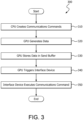
- Figure 3 is a flow chart showing an example method 300 which illustrates aspects of GPU remote communication, and can be employed, for example, using example topology 200 and/or example device 100.
- a CPU (such as CPU 210) of a computer system generates one or more communications commands, such as remote put commands (such as remote put commands 215), and stores these commands in a queue on a NIC (such as NIC 240) or other interface device.
- Each communications command includes a pointer to a send buffer.
- the send buffer is a portion of a system memory (such as system memory 230) of the computer system in this example.
- the send buffer could also be a portion of a GPU local memory, or another memory, in other implementations.
- a GPU (such as GPU 220) of the computer system generates data for communication to a GPU of another computer system.
- the GPU can execute a kernel which yields data for consumption by a remote GPU.
- the GPU stores the generated data in the send buffer.
- the GPU signals the NIC that data is ready in the send buffer.
- the GPU signals that data is ready to send by decrementing a counter variable stored in a memory, such as the NIC's device memory, or system memory.
- the GPU can signal the NIC or other interface device that data is ready in the send buffer in any other suitable way, such as by setting a value of a register in the device memory of the NIC or in the main system memory.
- the interface device executes one of the communications commands based on the signal from the GPU. For example, if the signal is a decremented counter variable associated with a pre-generated put command, the interface device can compare the counter variable to a threshold included in the communications commands. If the counter variable matches the value of a stored threshold of one of the plurality of commands, the NIC executes that command. Executing the communications command causes the NIC to transmit data in the send buffer (e.g., at a location pointed to by a pointer in the communications command) to a target specified in the communications command (e.g., memory of a remote GPU) over a computer communications network.
- the send buffer e.g., at a location pointed to by a pointer in the communications command
- a target specified in the communications command e.g., memory of a remote GPU
- step 310 is shown sequentially with steps 320-350.
- CPU creation of communications commands can also occur at any suitable time prior to, and independent of the other steps. This can have the advantage of removing the CPU from the critical path of RDMA operations.
- Figure 4 is a flow chart showing an example method 400 which illustrates aspects of GPU remote communication, and can be employed for example using a GPU in example topology 200 and/or example device 100.
- a GPU executes a kernel and generates data for transmission to a remote memory location over a computer communications network.
- the remote memory location may be a device memory of a remote GPU, system memory of a remote device that is accessible to a remote GPU, or any suitable RDMA target.
- the GPU On a condition 420 that the data is available (e.g., the GPU has completed executing the kernel or a particular workgroup, yielding data for transmission to a remote memory), the GPU writes the data to a send buffer in step 430.
- the send buffer is implemented in system memory.
- the send buffer can also be implemented in any suitable memory, such as a device memory of the GPU.
- the GPU triggers an interface device to transmit the data in the send buffer over a computer communications network to the remote GPU or other target using any suitable signaling technique, such as those described herein.
- the GPU may decrement a counter variable to signal the interface device to execute a pre-stored remote put command having an associated threshold value which matches the decremented counter variable.
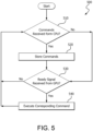
- Figure 5 is a flow chart showing an example method 500 which illustrates aspects of GPU remote communication, and can be employed for example using a NIC in example topology 200 and/or example device 100.
- the NIC On a condition 510 that a NIC receives pre-generated remote put commands from a CPU, the NIC stores the remote put commands in its device memory in step 520. Otherwise, or after storing the remote put commands, the NIC determines whether a data ready signal has been received from a GPU. For example, the NIC may compare the value of a counter variable in system memory, which can be decremented by the GPU, to a threshold value of one or more of the remote put commands, or may test the value of a flag or doorbell buffer which can be set by the GPU.
- the NIC executes the pre-stored remote put command to transmit data stored in a send buffer at an address indicated by a pointer in the remote put command over a computer communications network to a memory in a remote system, such as a GPU memory, system memory, or other suitable RDMA target.
- a remote system such as a GPU memory, system memory, or other suitable RDMA target.
- the NIC can then resume monitoring for new ready signals from the GPU or pre-generated communications commands from the CPU.
- Steps 510 and 520 do not necessarily execute sequentially with steps 530 and 540.
- the NIC can monitor for a ready signal from the GPU in step 530 indefinitely without receiving any additional pre-generated put commands in step 510.
- CPU creation of communications commands can occur at any suitable time prior to, and independent of the other steps. This can have the advantage of removing the CPU from the critical path of RDMA operations.
- Figure 6 is a flow chart showing an example method 600 which illustrates aspects of GPU remote communication, and can be employed for example using a CPU in example topology 200 and/or example device 100.
- a future communications pattern for the output of a GPU is determined or predicted.
- a CPU generates one or more communications commands based on the communications pattern.
- the communications commands can be remote put commands, for example, and can include a pointer to a send buffer which will store data from a GPU, information indicating a destination for the data, and possibly a counter value or other trigger information.
- the CPU transmits the communications commands to an NIC or other suitable interface device for storage in a device memory of the NIC or other suitable memory.
- processors include, by way of example, a general purpose processor, a special purpose processor, a conventional processor, a digital signal processor (DSP), a plurality of microprocessors, one or more microprocessors in association with a DSP core, a controller, a microcontroller, Application Specific Integrated Circuits (ASICs), Field Programmable Gate Arrays (FPGAs) circuits, any other type of integrated circuit (IC), and/or a state machine.
- DSP digital signal processor
- ASICs Application Specific Integrated Circuits
- FPGAs Field Programmable Gate Arrays
- Such processors can be manufactured by configuring a manufacturing process using the results of processed hardware description language (HDL) instructions and other intermediary data including netlists (such instructions capable of being stored on a computer readable media). The results of such processing can be maskworks that are then used in a semiconductor manufacturing process to manufacture a processor which implements aspects of the embodiments.
- HDL hardware description language
- non-transitory computer-readable storage mediums include a read only memory (ROM), a random access memory (RAM), a register, cache memory, semiconductor memory devices, magnetic media such as internal hard disks and removable disks, magneto-optical media, and optical media such as CD-ROM disks, and digital versatile disks (DVDs).
- ROM read only memory
- RAM random access memory
- register cache memory
- semiconductor memory devices magnetic media such as internal hard disks and removable disks, magneto-optical media, and optical media such as CD-ROM disks, and digital versatile disks (DVDs).
Landscapes
- Engineering & Computer Science (AREA)
- Theoretical Computer Science (AREA)
- Physics & Mathematics (AREA)
- General Physics & Mathematics (AREA)
- General Engineering & Computer Science (AREA)
- Signal Processing (AREA)
- Computer Networks & Wireless Communication (AREA)
- Computer Hardware Design (AREA)
- Mathematical Physics (AREA)
- Software Systems (AREA)
- Computer And Data Communications (AREA)
- Information Transfer Systems (AREA)
- Data Exchanges In Wide-Area Networks (AREA)
- Bus Control (AREA)
Claims (15)
- Verfahren zum Übertragen von Daten, das Verfahren umfassend:Empfangen, durch eine Schnittstellenvorrichtung (240), eines vorgenerierten Netzwerkfernkommunikationsbefehls (215) von einer zentralen Verarbeitungseinheit (CPU) (210), wobei der vorgenerierte Netzwerkfernkommunikationsbefehl einen Schwellenwert einschließt, der eine Anzahl von Auslösern angibt, um vor einem Ausführen des vorgenerierten Netzwerkfernkommunikationsbefehls zu warten;Empfangen, durch die Schnittstellenvorrichtung, eines Signals von einer Grafikverarbeitungseinheit (GPU) (220), das angibt, dass Daten in einem Speicher bereit sind, wobei das Signal einen Auslöser umfasst;Bestimmen, dass, nach dem Empfangen des Auslösers von der GPU, eine Anzahl von Auslösern, die durch die Schnittstellenvorrichtung empfangen werden, mit dem Schwellenwert übereinstimmt, der in dem vorgenerierten Netzwerkfernkommunikationsbefehl eingeschlossen ist; undals Reaktion auf das Bestimmen, Ausführen, durch die Schnittstellenvorrichtung, des vorgenerierten Netzwerkfernkommunikationsbefehls, um die Daten über ein Netzwerk an eine Zielvorrichtung zu übertragen.
- Verfahren nach Anspruch 1, wobei der vorgenerierte Netzwerkfernkommunikationsbefehl einen PUT-Befehl (215) und/oder einen Zählervariablenschwellenwert und/oder einen Zeiger auf eine Adresse in dem Speicher umfasst.
- Verfahren nach Anspruch 1, wobei das Signal eine Änderung eines Werts einer Zählervariable angibt.
- Verfahren nach Anspruch 1, wobei der vorgenerierte Netzwerkfernkommunikationsbefehl Informationen umfasst, die die Zielvorrichtung angeben.
- Verfahren nach Anspruch 4, wobei die Informationen Metadaten umfassen.
- Verfahren nach Anspruch 1, wobei die Schnittstellenvorrichtung einen Netzwerkschnittstellencontroller (NIC) (240) umfasst.
- Schnittstellenvorrichtung (240) zum Übertragen von Daten, die Vorrichtung umfassend:Empfängerschaltung, die konfiguriert ist, um einen vorgenerierten Netzwerkfernkommunikationsbefehl (215) von einer zentralen Verarbeitungseinheit (CPU) (210) zu empfangen, wobei der vorgenerierte Netzwerkfernkommunikationsbefehl einen Schwellenwert einschließt, der eine Anzahl von Auslösern angibt, um vor dem Ausführen des vorgenerierten Netzwerkfernkommunikationsbefehls zu warten;wobei die Empfängerschaltung ferner konfiguriert ist, um ein Signal von einer Grafikverarbeitungseinheit (GPU) (220) zu empfangen, das angibt, dass Daten in einem Speicher bereit sind, wobei das Signal einen Auslöser umfasst;Verarbeitungsschaltung, die konfiguriert ist, um zu bestimmen, dass, nachdem die Empfängerschaltung den Auslöser von der GPU empfängt, eine Anzahl von Auslösern, die durch die Empfängerschaltung empfangen werden, mit dem Schwellenwert übereinstimmt, der in dem vorgenerierten Netzwerkfernkommunikationsbefehl gespeichert ist, und, als Reaktion auf das Bestimmen, Ausführen des vorgenerierten Netzwerkfernkommunikationsbefehls; undSenderschaltung, die konfiguriert ist, um die Daten auf eine Zielvorrichtung über ein Netzwerk basierend auf dem vorgenerierten Netzwerkfernkommunikationsbefehl zu übertragen.
- Vorrichtung nach Anspruch 7, wobei der vorgenerierte Netzwerkfernkommunikationsbefehl einen PUT-Befehl und/oder einen Zählervariablenschwellenwert und/oder einen Zeiger auf eine Adresse in dem Speicher umfasst.
- Vorrichtung nach Anspruch 7, wobei das Signal eine Änderung eines Werts einer Zählervariable angibt.
- Vorrichtung nach Anspruch 7, wobei der vorgenerierte Fernkommunikationsnetzwerkbefehl Informationen umfasst, die die Zielvorrichtung angeben.
- Vorrichtung nach Anspruch 10, wobei die Informationen Metadaten umfassen.
- Vorrichtung nach Anspruch 7, wobei die Schnittstellenvorrichtung einen Netzwerkschnittstellencontroller (NIC) (240) umfasst.
- System zum Übertragen von Daten, das System umfassend:eine Schnittstellenvorrichtung (240);eine zentrale Verarbeitungseinheit (CPU) (210); undeine Grafikverarbeitungseinheit (GPU) (220);wobei:die CPU umfassend die Verarbeitungsschaltung, die konfiguriert ist, um einen vorgenerierten Netzwerkfernkommunikationsbefehl zu generieren, und die Senderschaltung, die konfiguriert ist, um den vorgenerierten Netzwerkfernkommunikationsbefehl an die Schnittstellenvorrichtung zu übertragen, wobei der vorgenerierte Netzwerkfernkommunikationsbefehl einen Schwellenwert einschließt, der eine Anzahl von Auslösern angibt, um vor dem Ausführen des vorgenerierten Netzwerkfernkommunikationsbefehls zu warten; unddie GPU umfassend die Verarbeitungsschaltung, die konfiguriert ist, um Daten für eine Übertragung an eine Zielvorrichtung über ein Netzwerk zu generieren, eine Speicherungsschaltung, die konfiguriert ist, um Daten in einem Puffer zu speichern, und die Senderschaltung, die konfiguriert ist, um an die Schnittstellenvorrichtung zu signalisieren, dass die Daten in dem Puffer gespeichert werden, sodass die Schnittstellenvorrichtung den vorgenerierten Netzwerkfernkommunikationsbefehl ausführt.
- System nach Anspruch 13, wobei die CPU und die GPU auf einem einzigen Chip und/oder innerhalb des selben Pakets angeordnet sind.
- System nach Anspruch 13, wobei die Schnittstellenvorrichtung einen Netzwerkschnittstellencontroller (NIC) (240) umfasst.
Applications Claiming Priority (2)
| Application Number | Priority Date | Filing Date | Title |
|---|---|---|---|
| US15/297,079 US10936533B2 (en) | 2016-10-18 | 2016-10-18 | GPU remote communication with triggered operations |
| PCT/US2017/052250 WO2018075182A1 (en) | 2016-10-18 | 2017-09-19 | Gpu remote communication with triggered operations |
Publications (3)
| Publication Number | Publication Date |
|---|---|
| EP3529706A1 EP3529706A1 (de) | 2019-08-28 |
| EP3529706A4 EP3529706A4 (de) | 2020-03-25 |
| EP3529706B1 true EP3529706B1 (de) | 2023-03-22 |
Family
ID=61904564
Family Applications (1)
| Application Number | Title | Priority Date | Filing Date |
|---|---|---|---|
| EP17862965.5A Active EP3529706B1 (de) | 2016-10-18 | 2017-09-19 | Gpu-fernkommunikation mit ausgelösten operationen |
Country Status (6)
| Country | Link |
|---|---|
| US (1) | US10936533B2 (de) |
| EP (1) | EP3529706B1 (de) |
| JP (1) | JP6961686B2 (de) |
| KR (1) | KR102245247B1 (de) |
| CN (1) | CN109690512B (de) |
| WO (1) | WO2018075182A1 (de) |
Families Citing this family (14)
| Publication number | Priority date | Publication date | Assignee | Title |
|---|---|---|---|---|
| US10534606B2 (en) | 2011-12-08 | 2020-01-14 | Oracle International Corporation | Run-length encoding decompression |
| US11113054B2 (en) | 2013-09-10 | 2021-09-07 | Oracle International Corporation | Efficient hardware instructions for single instruction multiple data processors: fast fixed-length value compression |
| US10599488B2 (en) | 2016-06-29 | 2020-03-24 | Oracle International Corporation | Multi-purpose events for notification and sequence control in multi-core processor systems |
| US10380058B2 (en) | 2016-09-06 | 2019-08-13 | Oracle International Corporation | Processor core to coprocessor interface with FIFO semantics |
| US10783102B2 (en) | 2016-10-11 | 2020-09-22 | Oracle International Corporation | Dynamically configurable high performance database-aware hash engine |
| US10459859B2 (en) | 2016-11-28 | 2019-10-29 | Oracle International Corporation | Multicast copy ring for database direct memory access filtering engine |
| US10725947B2 (en) | 2016-11-29 | 2020-07-28 | Oracle International Corporation | Bit vector gather row count calculation and handling in direct memory access engine |
| US20190044809A1 (en) * | 2017-08-30 | 2019-02-07 | Intel Corporation | Technologies for managing a flexible host interface of a network interface controller |
| US11429413B2 (en) * | 2018-03-30 | 2022-08-30 | Intel Corporation | Method and apparatus to manage counter sets in a network interface controller |
| US10740163B2 (en) | 2018-06-28 | 2020-08-11 | Advanced Micro Devices, Inc. | Network packet templating for GPU-initiated communication |
| US10795840B2 (en) | 2018-11-12 | 2020-10-06 | At&T Intellectual Property I, L.P. | Persistent kernel for graphics processing unit direct memory access network packet processing |
| DE112020002497T5 (de) * | 2019-05-23 | 2022-04-28 | Hewlett Packard Enterprise Development Lp | System und verfahren zur dynamischen zuweisung von reduktionsmotoren |
| US11182221B1 (en) * | 2020-12-18 | 2021-11-23 | SambaNova Systems, Inc. | Inter-node buffer-based streaming for reconfigurable processor-as-a-service (RPaaS) |
| US11960813B2 (en) | 2021-08-02 | 2024-04-16 | Advanced Micro Devices, Inc. | Automatic redistribution layer via generation |
Family Cites Families (27)
| Publication number | Priority date | Publication date | Assignee | Title |
|---|---|---|---|---|
| US5278956A (en) | 1990-01-22 | 1994-01-11 | Vlsi Technology, Inc. | Variable sized FIFO memory and programmable trigger level therefor for use in a UART or the like |
| US8766993B1 (en) | 2005-04-06 | 2014-07-01 | Teradici Corporation | Methods and apparatus for enabling multiple remote displays |
| JP4439491B2 (ja) | 2006-05-24 | 2010-03-24 | 株式会社ソニー・コンピュータエンタテインメント | マルチグラフィックスプロセッサシステム、グラフィックスプロセッサおよびデータ転送方法 |
| US8269782B2 (en) | 2006-11-10 | 2012-09-18 | Sony Computer Entertainment Inc. | Graphics processing apparatus |
| US8131814B1 (en) | 2008-07-11 | 2012-03-06 | Hewlett-Packard Development Company, L.P. | Dynamic pinning remote direct memory access |
| US20100013839A1 (en) * | 2008-07-21 | 2010-01-21 | Rawson Andrew R | Integrated GPU, NIC and Compression Hardware for Hosted Graphics |
| CN101539902B (zh) * | 2009-05-05 | 2012-03-28 | 中国科学院计算技术研究所 | 多计算机系统中节点的dma设备及通信方法 |
| US20100325372A1 (en) * | 2009-06-17 | 2010-12-23 | Housty Oswin E | Parallel training of dynamic random access memory channel controllers |
| US8937622B2 (en) * | 2010-09-20 | 2015-01-20 | Qualcomm Incorporated | Inter-processor communication techniques in a multiple-processor computing platform |
| US8902228B2 (en) * | 2011-09-19 | 2014-12-02 | Qualcomm Incorporated | Optimizing resolve performance with tiling graphics architectures |
| US9830288B2 (en) | 2011-12-19 | 2017-11-28 | Nvidia Corporation | System and method for transmitting graphics rendered on a primary computer to a secondary computer |
| WO2013095475A1 (en) * | 2011-12-21 | 2013-06-27 | Intel Corporation | Apparatus and method for memory-hierarchy aware producer-consumer instruction |
| US9171348B2 (en) * | 2012-01-23 | 2015-10-27 | Google Inc. | Rendering content on computing systems |
| ITRM20120094A1 (it) | 2012-03-14 | 2013-09-14 | Istituto Naz Di Fisica Nuclea Re | Scheda di interfaccia di rete per nodo di rete di calcolo parallelo su gpu, e relativo metodo di comunicazione internodale |
| US9602437B1 (en) * | 2012-10-03 | 2017-03-21 | Tracey M. Bernath | System and method for accelerating network applications using an enhanced network interface and massively parallel distributed processing |
| US9582402B2 (en) | 2013-05-01 | 2017-02-28 | Advanced Micro Devices, Inc. | Remote task queuing by networked computing devices |
| US10134102B2 (en) * | 2013-06-10 | 2018-11-20 | Sony Interactive Entertainment Inc. | Graphics processing hardware for using compute shaders as front end for vertex shaders |
| WO2015130282A1 (en) * | 2014-02-27 | 2015-09-03 | Hewlett-Packard Development Company, L. P. | Communication between integrated graphics processing units |
| US10218645B2 (en) * | 2014-04-08 | 2019-02-26 | Mellanox Technologies, Ltd. | Low-latency processing in a network node |
| US10331595B2 (en) * | 2014-10-23 | 2019-06-25 | Mellanox Technologies, Ltd. | Collaborative hardware interaction by multiple entities using a shared queue |
| US9582463B2 (en) | 2014-12-09 | 2017-02-28 | Intel Corporation | Heterogeneous input/output (I/O) using remote direct memory access (RDMA) and active message |
| US9779466B2 (en) * | 2015-05-07 | 2017-10-03 | Microsoft Technology Licensing, Llc | GPU operation |
| US10248610B2 (en) * | 2015-06-23 | 2019-04-02 | Mellanox Technologies, Ltd. | Enforcing transaction order in peer-to-peer interactions |
| US10445850B2 (en) * | 2015-08-26 | 2019-10-15 | Intel Corporation | Technologies for offloading network packet processing to a GPU |
| US10210593B2 (en) * | 2016-01-28 | 2019-02-19 | Qualcomm Incorporated | Adaptive context switching |
| US10331590B2 (en) * | 2016-06-30 | 2019-06-25 | Intel Corporation | Graphics processing unit (GPU) as a programmable packet transfer mechanism |
| US10410313B2 (en) * | 2016-08-05 | 2019-09-10 | Qualcomm Incorporated | Dynamic foveation adjustment |
-
2016
- 2016-10-18 US US15/297,079 patent/US10936533B2/en active Active
-
2017
- 2017-09-19 KR KR1020197007796A patent/KR102245247B1/ko active IP Right Grant
- 2017-09-19 JP JP2019517022A patent/JP6961686B2/ja active Active
- 2017-09-19 EP EP17862965.5A patent/EP3529706B1/de active Active
- 2017-09-19 WO PCT/US2017/052250 patent/WO2018075182A1/en unknown
- 2017-09-19 CN CN201780056487.7A patent/CN109690512B/zh active Active
Also Published As
| Publication number | Publication date |
|---|---|
| CN109690512B (zh) | 2023-07-18 |
| US10936533B2 (en) | 2021-03-02 |
| KR102245247B1 (ko) | 2021-04-27 |
| EP3529706A1 (de) | 2019-08-28 |
| EP3529706A4 (de) | 2020-03-25 |
| WO2018075182A1 (en) | 2018-04-26 |
| US20180107627A1 (en) | 2018-04-19 |
| CN109690512A (zh) | 2019-04-26 |
| KR20190058483A (ko) | 2019-05-29 |
| JP6961686B2 (ja) | 2021-11-05 |
| JP2019532427A (ja) | 2019-11-07 |
Similar Documents
| Publication | Publication Date | Title |
|---|---|---|
| EP3529706B1 (de) | Gpu-fernkommunikation mit ausgelösten operationen | |
| US9881680B2 (en) | Multi-host power controller (MHPC) of a flash-memory-based storage device | |
| US20160371222A1 (en) | COHERENCY DRIVEN ENHANCEMENTS TO A PERIPHERAL COMPONENT INTERCONNECT (PCI) EXPRESS (PCIe) TRANSACTION LAYER | |
| US20170123670A1 (en) | Method and systems of controlling memory-to-memory copy operations | |
| WO2019141157A1 (zh) | 一种核间数据传输的装置和方法 | |
| EP3134805B1 (de) | Latenzbasierte energiemoduseinheiten zur steuerung von leistungsmodi von prozessorkernen sowie entsprechende verfahren und systeme | |
| US20170178275A1 (en) | Method and system for using solid state device as eviction pad for graphics processing unit | |
| CN116601616A (zh) | 一种数据处理装置、方法及相关设备 | |
| US8959296B2 (en) | Method and apparatus for centralized timestamp processing | |
| US9880748B2 (en) | Bifurcated memory management for memory elements | |
| US11210248B2 (en) | System direct memory access engine offload | |
| JP6396625B1 (ja) | 複数のマスタデバイス間の条件付き介入を使用したキャッシュコヒーレンシの維持 | |
| WO2023009308A1 (en) | Hierarchical state save and restore for device with varying power states | |
| US10445275B2 (en) | System on chip having integrated solid state graphics controllers | |
| JP2021064166A (ja) | メモリ制御装置、および制御方法 |
Legal Events
| Date | Code | Title | Description |
|---|---|---|---|
| STAA | Information on the status of an ep patent application or granted ep patent |
Free format text: STATUS: THE INTERNATIONAL PUBLICATION HAS BEEN MADE |
|
| PUAI | Public reference made under article 153(3) epc to a published international application that has entered the european phase |
Free format text: ORIGINAL CODE: 0009012 |
|
| STAA | Information on the status of an ep patent application or granted ep patent |
Free format text: STATUS: REQUEST FOR EXAMINATION WAS MADE |
|
| 17P | Request for examination filed |
Effective date: 20190326 |
|
| AK | Designated contracting states |
Kind code of ref document: A1 Designated state(s): AL AT BE BG CH CY CZ DE DK EE ES FI FR GB GR HR HU IE IS IT LI LT LU LV MC MK MT NL NO PL PT RO RS SE SI SK SM TR |
|
| AX | Request for extension of the european patent |
Extension state: BA ME |
|
| DAV | Request for validation of the european patent (deleted) | ||
| DAX | Request for extension of the european patent (deleted) | ||
| A4 | Supplementary search report drawn up and despatched |
Effective date: 20200226 |
|
| RIC1 | Information provided on ipc code assigned before grant |
Ipc: G06F 13/38 20060101AFI20200220BHEP |
|
| STAA | Information on the status of an ep patent application or granted ep patent |
Free format text: STATUS: EXAMINATION IS IN PROGRESS |
|
| 17Q | First examination report despatched |
Effective date: 20210222 |
|
| STAA | Information on the status of an ep patent application or granted ep patent |
Free format text: STATUS: EXAMINATION IS IN PROGRESS |
|
| GRAP | Despatch of communication of intention to grant a patent |
Free format text: ORIGINAL CODE: EPIDOSNIGR1 |
|
| STAA | Information on the status of an ep patent application or granted ep patent |
Free format text: STATUS: GRANT OF PATENT IS INTENDED |
|
| INTG | Intention to grant announced |
Effective date: 20221007 |
|
| GRAS | Grant fee paid |
Free format text: ORIGINAL CODE: EPIDOSNIGR3 |
|
| GRAA | (expected) grant |
Free format text: ORIGINAL CODE: 0009210 |
|
| STAA | Information on the status of an ep patent application or granted ep patent |
Free format text: STATUS: THE PATENT HAS BEEN GRANTED |
|
| AK | Designated contracting states |
Kind code of ref document: B1 Designated state(s): AL AT BE BG CH CY CZ DE DK EE ES FI FR GB GR HR HU IE IS IT LI LT LU LV MC MK MT NL NO PL PT RO RS SE SI SK SM TR |
|
| REG | Reference to a national code |
Ref country code: GB Ref legal event code: FG4D |
|
| REG | Reference to a national code |
Ref country code: CH Ref legal event code: EP |
|
| REG | Reference to a national code |
Ref country code: IE Ref legal event code: FG4D |
|
| REG | Reference to a national code |
Ref country code: DE Ref legal event code: R096 Ref document number: 602017067084 Country of ref document: DE |
|
| REG | Reference to a national code |
Ref country code: AT Ref legal event code: REF Ref document number: 1555728 Country of ref document: AT Kind code of ref document: T Effective date: 20230415 |
|
| REG | Reference to a national code |
Ref country code: LT Ref legal event code: MG9D |
|
| P01 | Opt-out of the competence of the unified patent court (upc) registered |
Effective date: 20230530 |
|
| REG | Reference to a national code |
Ref country code: NL Ref legal event code: MP Effective date: 20230322 |
|
| PG25 | Lapsed in a contracting state [announced via postgrant information from national office to epo] |
Ref country code: RS Free format text: LAPSE BECAUSE OF FAILURE TO SUBMIT A TRANSLATION OF THE DESCRIPTION OR TO PAY THE FEE WITHIN THE PRESCRIBED TIME-LIMIT Effective date: 20230322 Ref country code: NO Free format text: LAPSE BECAUSE OF FAILURE TO SUBMIT A TRANSLATION OF THE DESCRIPTION OR TO PAY THE FEE WITHIN THE PRESCRIBED TIME-LIMIT Effective date: 20230622 Ref country code: LV Free format text: LAPSE BECAUSE OF FAILURE TO SUBMIT A TRANSLATION OF THE DESCRIPTION OR TO PAY THE FEE WITHIN THE PRESCRIBED TIME-LIMIT Effective date: 20230322 Ref country code: LT Free format text: LAPSE BECAUSE OF FAILURE TO SUBMIT A TRANSLATION OF THE DESCRIPTION OR TO PAY THE FEE WITHIN THE PRESCRIBED TIME-LIMIT Effective date: 20230322 Ref country code: HR Free format text: LAPSE BECAUSE OF FAILURE TO SUBMIT A TRANSLATION OF THE DESCRIPTION OR TO PAY THE FEE WITHIN THE PRESCRIBED TIME-LIMIT Effective date: 20230322 |
|
| REG | Reference to a national code |
Ref country code: AT Ref legal event code: MK05 Ref document number: 1555728 Country of ref document: AT Kind code of ref document: T Effective date: 20230322 |
|
| PG25 | Lapsed in a contracting state [announced via postgrant information from national office to epo] |
Ref country code: SE Free format text: LAPSE BECAUSE OF FAILURE TO SUBMIT A TRANSLATION OF THE DESCRIPTION OR TO PAY THE FEE WITHIN THE PRESCRIBED TIME-LIMIT Effective date: 20230322 Ref country code: NL Free format text: LAPSE BECAUSE OF FAILURE TO SUBMIT A TRANSLATION OF THE DESCRIPTION OR TO PAY THE FEE WITHIN THE PRESCRIBED TIME-LIMIT Effective date: 20230322 Ref country code: GR Free format text: LAPSE BECAUSE OF FAILURE TO SUBMIT A TRANSLATION OF THE DESCRIPTION OR TO PAY THE FEE WITHIN THE PRESCRIBED TIME-LIMIT Effective date: 20230623 Ref country code: FI Free format text: LAPSE BECAUSE OF FAILURE TO SUBMIT A TRANSLATION OF THE DESCRIPTION OR TO PAY THE FEE WITHIN THE PRESCRIBED TIME-LIMIT Effective date: 20230322 |
|
| PG25 | Lapsed in a contracting state [announced via postgrant information from national office to epo] |
Ref country code: SM Free format text: LAPSE BECAUSE OF FAILURE TO SUBMIT A TRANSLATION OF THE DESCRIPTION OR TO PAY THE FEE WITHIN THE PRESCRIBED TIME-LIMIT Effective date: 20230322 Ref country code: RO Free format text: LAPSE BECAUSE OF FAILURE TO SUBMIT A TRANSLATION OF THE DESCRIPTION OR TO PAY THE FEE WITHIN THE PRESCRIBED TIME-LIMIT Effective date: 20230322 Ref country code: PT Free format text: LAPSE BECAUSE OF FAILURE TO SUBMIT A TRANSLATION OF THE DESCRIPTION OR TO PAY THE FEE WITHIN THE PRESCRIBED TIME-LIMIT Effective date: 20230724 Ref country code: ES Free format text: LAPSE BECAUSE OF FAILURE TO SUBMIT A TRANSLATION OF THE DESCRIPTION OR TO PAY THE FEE WITHIN THE PRESCRIBED TIME-LIMIT Effective date: 20230322 Ref country code: EE Free format text: LAPSE BECAUSE OF FAILURE TO SUBMIT A TRANSLATION OF THE DESCRIPTION OR TO PAY THE FEE WITHIN THE PRESCRIBED TIME-LIMIT Effective date: 20230322 Ref country code: AT Free format text: LAPSE BECAUSE OF FAILURE TO SUBMIT A TRANSLATION OF THE DESCRIPTION OR TO PAY THE FEE WITHIN THE PRESCRIBED TIME-LIMIT Effective date: 20230322 |
|
| PGFP | Annual fee paid to national office [announced via postgrant information from national office to epo] |
Ref country code: GB Payment date: 20230912 Year of fee payment: 7 |
|
| PG25 | Lapsed in a contracting state [announced via postgrant information from national office to epo] |
Ref country code: SK Free format text: LAPSE BECAUSE OF FAILURE TO SUBMIT A TRANSLATION OF THE DESCRIPTION OR TO PAY THE FEE WITHIN THE PRESCRIBED TIME-LIMIT Effective date: 20230322 Ref country code: PL Free format text: LAPSE BECAUSE OF FAILURE TO SUBMIT A TRANSLATION OF THE DESCRIPTION OR TO PAY THE FEE WITHIN THE PRESCRIBED TIME-LIMIT Effective date: 20230322 Ref country code: IS Free format text: LAPSE BECAUSE OF FAILURE TO SUBMIT A TRANSLATION OF THE DESCRIPTION OR TO PAY THE FEE WITHIN THE PRESCRIBED TIME-LIMIT Effective date: 20230722 |
|
| REG | Reference to a national code |
Ref country code: DE Ref legal event code: R097 Ref document number: 602017067084 Country of ref document: DE |
|
| PLBE | No opposition filed within time limit |
Free format text: ORIGINAL CODE: 0009261 |
|
| STAA | Information on the status of an ep patent application or granted ep patent |
Free format text: STATUS: NO OPPOSITION FILED WITHIN TIME LIMIT |
|
| PG25 | Lapsed in a contracting state [announced via postgrant information from national office to epo] |
Ref country code: SI Free format text: LAPSE BECAUSE OF FAILURE TO SUBMIT A TRANSLATION OF THE DESCRIPTION OR TO PAY THE FEE WITHIN THE PRESCRIBED TIME-LIMIT Effective date: 20230322 Ref country code: DK Free format text: LAPSE BECAUSE OF FAILURE TO SUBMIT A TRANSLATION OF THE DESCRIPTION OR TO PAY THE FEE WITHIN THE PRESCRIBED TIME-LIMIT Effective date: 20230322 Ref country code: CZ Free format text: LAPSE BECAUSE OF FAILURE TO SUBMIT A TRANSLATION OF THE DESCRIPTION OR TO PAY THE FEE WITHIN THE PRESCRIBED TIME-LIMIT Effective date: 20230322 |
|
| 26N | No opposition filed |
Effective date: 20240102 |
|
| PGFP | Annual fee paid to national office [announced via postgrant information from national office to epo] |
Ref country code: DE Payment date: 20240308 Year of fee payment: 7 |
|
| REG | Reference to a national code |
Ref country code: CH Ref legal event code: PL |