EP3528286A1 - Display device and manufacturing method therefor - Google Patents
Display device and manufacturing method therefor Download PDFInfo
- Publication number
- EP3528286A1 EP3528286A1 EP17881307.7A EP17881307A EP3528286A1 EP 3528286 A1 EP3528286 A1 EP 3528286A1 EP 17881307 A EP17881307 A EP 17881307A EP 3528286 A1 EP3528286 A1 EP 3528286A1
- Authority
- EP
- European Patent Office
- Prior art keywords
- polysilicon
- display device
- conductive layer
- pixel
- patterned
- Prior art date
- Legal status (The legal status is an assumption and is not a legal conclusion. Google has not performed a legal analysis and makes no representation as to the accuracy of the status listed.)
- Granted
Links
Images


Classifications
-
- H—ELECTRICITY
- H10—SEMICONDUCTOR DEVICES; ELECTRIC SOLID-STATE DEVICES NOT OTHERWISE PROVIDED FOR
- H10D—INORGANIC ELECTRIC SEMICONDUCTOR DEVICES
- H10D86/00—Integrated devices formed in or on insulating or conducting substrates, e.g. formed in silicon-on-insulator [SOI] substrates or on stainless steel or glass substrates
-
- G—PHYSICS
- G09—EDUCATION; CRYPTOGRAPHY; DISPLAY; ADVERTISING; SEALS
- G09G—ARRANGEMENTS OR CIRCUITS FOR CONTROL OF INDICATING DEVICES USING STATIC MEANS TO PRESENT VARIABLE INFORMATION
- G09G3/00—Control arrangements or circuits, of interest only in connection with visual indicators other than cathode-ray tubes
- G09G3/20—Control arrangements or circuits, of interest only in connection with visual indicators other than cathode-ray tubes for presentation of an assembly of a number of characters, e.g. a page, by composing the assembly by combination of individual elements arranged in a matrix no fixed position being assigned to or needed to be assigned to the individual characters or partial characters
-
- H—ELECTRICITY
- H10—SEMICONDUCTOR DEVICES; ELECTRIC SOLID-STATE DEVICES NOT OTHERWISE PROVIDED FOR
- H10D—INORGANIC ELECTRIC SEMICONDUCTOR DEVICES
- H10D30/00—Field-effect transistors [FET]
- H10D30/60—Insulated-gate field-effect transistors [IGFET]
- H10D30/67—Thin-film transistors [TFT]
- H10D30/6729—Thin-film transistors [TFT] characterised by the electrodes
- H10D30/673—Thin-film transistors [TFT] characterised by the electrodes characterised by the shapes, relative sizes or dispositions of the gate electrodes
- H10D30/6733—Multi-gate TFTs
-
- H—ELECTRICITY
- H10—SEMICONDUCTOR DEVICES; ELECTRIC SOLID-STATE DEVICES NOT OTHERWISE PROVIDED FOR
- H10D—INORGANIC ELECTRIC SEMICONDUCTOR DEVICES
- H10D84/00—Integrated devices formed in or on semiconductor substrates that comprise only semiconducting layers, e.g. on Si wafers or on GaAs-on-Si wafers
-
- H—ELECTRICITY
- H10—SEMICONDUCTOR DEVICES; ELECTRIC SOLID-STATE DEVICES NOT OTHERWISE PROVIDED FOR
- H10D—INORGANIC ELECTRIC SEMICONDUCTOR DEVICES
- H10D84/00—Integrated devices formed in or on semiconductor substrates that comprise only semiconducting layers, e.g. on Si wafers or on GaAs-on-Si wafers
- H10D84/01—Manufacture or treatment
-
- H—ELECTRICITY
- H10—SEMICONDUCTOR DEVICES; ELECTRIC SOLID-STATE DEVICES NOT OTHERWISE PROVIDED FOR
- H10D—INORGANIC ELECTRIC SEMICONDUCTOR DEVICES
- H10D86/00—Integrated devices formed in or on insulating or conducting substrates, e.g. formed in silicon-on-insulator [SOI] substrates or on stainless steel or glass substrates
- H10D86/01—Manufacture or treatment
- H10D86/021—Manufacture or treatment of multiple TFTs
- H10D86/0221—Manufacture or treatment of multiple TFTs comprising manufacture, treatment or patterning of TFT semiconductor bodies
-
- H—ELECTRICITY
- H10—SEMICONDUCTOR DEVICES; ELECTRIC SOLID-STATE DEVICES NOT OTHERWISE PROVIDED FOR
- H10D—INORGANIC ELECTRIC SEMICONDUCTOR DEVICES
- H10D86/00—Integrated devices formed in or on insulating or conducting substrates, e.g. formed in silicon-on-insulator [SOI] substrates or on stainless steel or glass substrates
- H10D86/40—Integrated devices formed in or on insulating or conducting substrates, e.g. formed in silicon-on-insulator [SOI] substrates or on stainless steel or glass substrates characterised by multiple TFTs
- H10D86/441—Interconnections, e.g. scanning lines
-
- H—ELECTRICITY
- H10—SEMICONDUCTOR DEVICES; ELECTRIC SOLID-STATE DEVICES NOT OTHERWISE PROVIDED FOR
- H10D—INORGANIC ELECTRIC SEMICONDUCTOR DEVICES
- H10D86/00—Integrated devices formed in or on insulating or conducting substrates, e.g. formed in silicon-on-insulator [SOI] substrates or on stainless steel or glass substrates
- H10D86/40—Integrated devices formed in or on insulating or conducting substrates, e.g. formed in silicon-on-insulator [SOI] substrates or on stainless steel or glass substrates characterised by multiple TFTs
- H10D86/481—Integrated devices formed in or on insulating or conducting substrates, e.g. formed in silicon-on-insulator [SOI] substrates or on stainless steel or glass substrates characterised by multiple TFTs integrated with passive devices, e.g. auxiliary capacitors
-
- H—ELECTRICITY
- H10—SEMICONDUCTOR DEVICES; ELECTRIC SOLID-STATE DEVICES NOT OTHERWISE PROVIDED FOR
- H10D—INORGANIC ELECTRIC SEMICONDUCTOR DEVICES
- H10D86/00—Integrated devices formed in or on insulating or conducting substrates, e.g. formed in silicon-on-insulator [SOI] substrates or on stainless steel or glass substrates
- H10D86/40—Integrated devices formed in or on insulating or conducting substrates, e.g. formed in silicon-on-insulator [SOI] substrates or on stainless steel or glass substrates characterised by multiple TFTs
- H10D86/60—Integrated devices formed in or on insulating or conducting substrates, e.g. formed in silicon-on-insulator [SOI] substrates or on stainless steel or glass substrates characterised by multiple TFTs wherein the TFTs are in active matrices
-
- H—ELECTRICITY
- H10—SEMICONDUCTOR DEVICES; ELECTRIC SOLID-STATE DEVICES NOT OTHERWISE PROVIDED FOR
- H10P—GENERIC PROCESSES OR APPARATUS FOR THE MANUFACTURE OR TREATMENT OF DEVICES COVERED BY CLASS H10
- H10P14/00—Formation of materials, e.g. in the shape of layers or pillars
- H10P14/40—Formation of materials, e.g. in the shape of layers or pillars of conductive or resistive materials
- H10P14/416—Formation of materials, e.g. in the shape of layers or pillars of conductive or resistive materials of highly doped semiconductor materials, e.g. polysilicon layers or amorphous silicon layers
-
- G—PHYSICS
- G09—EDUCATION; CRYPTOGRAPHY; DISPLAY; ADVERTISING; SEALS
- G09G—ARRANGEMENTS OR CIRCUITS FOR CONTROL OF INDICATING DEVICES USING STATIC MEANS TO PRESENT VARIABLE INFORMATION
- G09G2300/00—Aspects of the constitution of display devices
- G09G2300/04—Structural and physical details of display devices
- G09G2300/0404—Matrix technologies
- G09G2300/0408—Integration of the drivers onto the display substrate
-
- G—PHYSICS
- G09—EDUCATION; CRYPTOGRAPHY; DISPLAY; ADVERTISING; SEALS
- G09G—ARRANGEMENTS OR CIRCUITS FOR CONTROL OF INDICATING DEVICES USING STATIC MEANS TO PRESENT VARIABLE INFORMATION
- G09G2300/00—Aspects of the constitution of display devices
- G09G2300/04—Structural and physical details of display devices
- G09G2300/0421—Structural details of the set of electrodes
- G09G2300/0426—Layout of electrodes and connections
-
- G—PHYSICS
- G09—EDUCATION; CRYPTOGRAPHY; DISPLAY; ADVERTISING; SEALS
- G09G—ARRANGEMENTS OR CIRCUITS FOR CONTROL OF INDICATING DEVICES USING STATIC MEANS TO PRESENT VARIABLE INFORMATION
- G09G2300/00—Aspects of the constitution of display devices
- G09G2300/08—Active matrix structure, i.e. with use of active elements, inclusive of non-linear two terminal elements, in the pixels together with light emitting or modulating elements
-
- G—PHYSICS
- G09—EDUCATION; CRYPTOGRAPHY; DISPLAY; ADVERTISING; SEALS
- G09G—ARRANGEMENTS OR CIRCUITS FOR CONTROL OF INDICATING DEVICES USING STATIC MEANS TO PRESENT VARIABLE INFORMATION
- G09G2310/00—Command of the display device
- G09G2310/02—Addressing, scanning or driving the display screen or processing steps related thereto
- G09G2310/0264—Details of driving circuits
- G09G2310/0267—Details of drivers for scan electrodes, other than drivers for liquid crystal, plasma or OLED displays
Definitions
- the present invention relates to the field of display technology and, in particular, to a display device and a method for fabricating the display device.
- the gate-in-panel (GIP) technology is often adopted to directly integrate gate drive circuits (i.e., GIP circuits) in a display panel consisting typically of a display area for displaying images and a non-display area surrounding the display area.
- GIP circuits gate drive circuits
- a display panel consisting typically of a display area for displaying images and a non-display area surrounding the display area.
- a plurality of scan lines and a plurality of data lines crossing the scan lines are arranged, thus defining an array of pixel cells.
- the GIP circuits are provided in the non-display area and are connected to the pixel cells via the scan lines.
- display panels are increasingly diversified in terms of shape.
- display panels having different shapes such as polygonal and circular.
- watches typically use circular display panels.
- the number of pixels in each column and in each row is the same.
- it is impossible for a polygonal or circular display panel as the number of pixels may vary across different columns or rows in such display panels.
- the present invention provides a method for manufacturing a display device, comprising:
- the method may further comprise, during the patterning the polysilicon layer to form a plurality of polysilicon blocks, patterning the polysilicon layer to form a plurality of first plates of a plurality of pixel capacitors and a plurality of sources and drains of a plurality of thin film transistors.
- the method may further comprise, during the implanting ions into the plurality of polysilicon blocks, implanting ions into the first plates of the plurality of pixel capacitors.
- the method may further comprise, during patterning the first conductive layer to form a plurality of data lines, patterning the first conductive layer to form a plurality of second plates of the plurality of pixel capacitors and a plurality of gates of the plurality of thin film transistors.
- the method may further comprise, subsequent to the patterning the first conductive layer to form a plurality of data lines, forming a second conductive layer over the patterned first conductive layer and patterning the second conductive layer to form a plurality of pixel connection lines and a plurality of power lines.
- the method may further comprise, prior to the forming a second conductive layer over the patterned first conductive layer and subsequent to the patterning the first conductive layer to form a plurality of data lines, forming a plurality of contact holes in the polysilicon blocks for connecting of the power lines to the polysilicon blocks.
- an overlapped area of the data line and the polysilicon block may be adjusted based on a number of pixel cells connected to the data line.
- a corresponding display device comprising a substrate; and a patterned polysilicon layer, a patterned gate insulating layer and a patterned first conductive layer, stacked on the substrate in sequence, wherein the patterned polysilicon layer comprises a plurality of polysilicon blocks doped with impurities, the patterned first conductive layer comprising a plurality of data lines, each of the plurality of data lines partially overlapping a corresponding polysilicon block of the plurality of polysilicon blocks to form a compensating capacitor.
- the display device may further comprise a plurality of pixel cells each comprising a thin film transistor and a pixel capacitor, wherein sources and drains of the thin film transistors and first plates of the plurality of pixel capacitors are fabricated in the same process as the polysilicon blocks, and wherein gates of the thin film transistors and second plates of the pixel capacitors are fabricated in the same process as the data lines.
- the display device may further comprise a plurality of test circuits, wherein each of the data lines has a first end connected to a corresponding pixel cell of the plurality of pixel cells and a second end connected to a corresponding test circuit of the test circuits.
- the display device may further comprise a plurality of GIP circuits, a plurality of pixel connection lines and a plurality of power lines, the pixel connection lines and the power lines being situated in the same layer and made of the same material, the power lines being connected to the pixel cells and configured to provide pixel cells with a power supply signal, the pixel connection lines being configured to connect the pixel cells to the GIP circuits.
- the compensating capacitor may be provided to compensate for a parasitic capacitance of the data line, and wherein a compensating capacitance of the compensating capacitor is proportional to an overlapped area of the data line and the polysilicon block.
- the overlapped area of the data line and the polysilicon block may be related to a number of the pixel cells connected to the data line.
- the overlapped area between the doped polysilicon layer and the first conductive layer provides a compensating capacitor for the data line, so that a footprint of the compensating capacitor is reduced and hence the connection between the scan line and GIP circuit is facilitated.
- a method for manufacturing a display device includes the steps of:
- a substrate 100 is provided.
- the substrate 100 includes a display area and a non-display area surrounding the display area.
- the display area is formed with a pixel array including a plurality of pixel cells 101 arranged in a pattern of array.
- Each pixel cell 101 has a pixel capacitor and a thin film transistor (not shown).
- the non-display area is formed with a plurality of GIP circuits 140 and test circuits 150.
- a polysilicon layer is formed on the substrate 100 and patterned by an etching process to form a plurality of first plates (not shown) of the pixel capacitors in the pixel cells 101, sources and drains (not shown) of the thin film transistors in the pixel cells 101, and a plurality of polysilicon blocks 110 outside the pixel cells 101.
- the polysilicon blocks 110 are formed between the pixel cells 101 and the test circuits 150.
- the polysilicon blocks 110 are all formed in the non-display area.
- boron or phosphorus ions are implanted into the first plates of the pixel capacitors and into the polysilicon blocks 110.
- the first plate and the polysilicon block 110 are doped by ion implantation, the conductivity of the first plates and polysilicon blocks 110 are improved.
- a gate insulating layer is formed over the patterned polysilicon layer and is then patterned.
- a first conductive layer is formed over the patterned gate insulating layer and is then patterned by an etching process to form second plates (not shown) of the pixel capacitors, gates (not shown) of the thin film transistors and a plurality of data lines 120.
- Each of the data lines 120 is connected to a corresponding one of the pixel cells 101 at one end and to a corresponding one of the test circuits 150 at the other end.
- the data lines 120 partially overlap a corresponding one of the polysilicon blocks 110 to provide a compensating capacitor.
- the compensating capacitor has a capacitance proportional to an overlapped area of the data line 120 and the polysilicon block 110.
- the overlapped area of the data line 120 and the polysilicon block 110 could be adjusted according to the number of pixel cells 101 in connection with the corresponding data line 120.
- a contact hole fabrication process is performed to form a plurality of contact holes 110a in the polysilicon blocks 110.
- the contact holes 110a terminate within the polysilicon blocks 110, i.e., having a depth smaller than a thickness of the polysilicon blocks 110, so that the polysilicon blocks 110 are exposed at the bottoms of the contact holes 110a.
- a second conductive layer is formed over the patterned first conductive layer and is then patterned by an etching process to form power lines 131 and pixel connection lines 132.
- the power lines 131 are connected to the polysilicon blocks 110 via the contact holes 110a and the pixel connection lines 132 are configured to connect the pixel cells 101 to the GIP circuits 140.
- the materials of the first conductive layer and the second conductive layer are not limited to any particular materials and may be selected according to practical needs.
- the materials from which the first conductive layer and the second conductive layer are fabricated include transparent conductive materials such as indium tin oxide (ITO), indium zinc oxide (IZO), zirconium-doped zinc oxide (ZZO), fluorine-doped tin oxide (FTO), nano silver or the like and non-transparent conductive materials such as silver (Ag), aluminum (Al), tungsten, silver alloys, aluminum alloys or the like.
- each of the compensating capacitors is constructed with one plate provided by the conductive layer and another plate provided by a polysilicon block.
- both of the plates of compensating capacitor are provided by conductive layers.
- the compensating capacitor since one plate of the compensating capacitor is provided by a polysilicon block 110, the compensating capacitor has a reduced foot print and can be fabricated more easily. Moreover, the fabrication of the display device can be accomplished by using a two-metal process (involving the formation of two metal layers), dispensing with the need to employ a three-metal process (involving the formation of three metal layers).
- the display device 10 includes a substrate 100, a patterned polysilicon layer, a patterned gate insulating layer and a patterned first conductive layer stacked on the substrate 100 in sequence.
- the patterned polysilicon layer includes a plurality of polysilicon blocks 110.
- the patterned first conductive layer includes a plurality of data lines 120 each having a part overlapping a corresponding one of the polysilicon blocks 110 to form a compensating capacitor.
- the display device 10 also includes a plurality of scan lines (not shown) for providing scan signals and a plurality of data lines 120 for providing data signals.
- the scan lines cross the data lines 120 to form a plurality of pixel cells 101 each arranged in an array.
- Each of pixel cells 101 includes a pixel capacitor (not shown) and a thin film transistor (not shown).
- Second plates of the pixel capacitors and gates of the thin film transistors, together with data lines 120 (all located in the first conductive layer), are manufactured in the same process.
- First plates of the pixel capacitors and sources and drains of the thin film transistors and the polysilicon blocks 110 are fabricated in the same process.
- the patterned polysilicon layer and the patterned first conductive layer are partially overlapped (i.e., the data lines 120 partially overlapping with a corresponding one of the polysilicon blocks 110).
- the overlapped area of the polysilicon layer and the first conductive layer provides the opposing plates of the compensating capacitors, with the gate insulating layer between the polysilicon layer and the first conductive layer acting as the insulating dielectric of the compensating capacitor.
- the compensating capacitance is provided to compensate for parasitic capacitances of the data lines 120.
- the compensating capacitance of each of the compensating capacitors is proportional to an overlapped area of a corresponding one of the data lines 120 and a corresponding one of the polysilicon blocks 110.
- the overlapped area of the data line 120 and the polysilicon block 110 is related to the number of pixel cells 101 in connection with the data line 120. The more pixel cells 101 connected to the data line 120 are, the smaller overlapped area of the data line 120 and the polysilicon block 110 is, and hence the compensating capacitance the compensating capacitor provides is smaller. On the contrary, fewer pixel cells 101 connected to the data line 120, the greater the overlapped area of the data line 120 and the polysilicon block 110 is, and therefore the compensating capacitance provided by the compensating capacitor would be greater.
- a data signal supplied to the pixel cells 101 from the data line 120 is also applied to one plate of the compensating capacitor, to compensate a parasitic capacitance compensation of the data line 120. Since the compensating capacitances provided by the compensating capacitors depend on the numbers of pixel cells 101 connected to the data lines 120, the parasitic capacitance compensation for the data lines 120 could be effectively achieved even if the number of pixel cells in different columns is different. Thus, display unevenness could be always avoided.
- the display device 10 further includes a plurality of power lines 131 connected at one end to the pixel cells 101 so as to provide the pixel cells with a power supply signal. Additionally, a plurality of contact holes 110a are provided in the polysilicon blocks 110. The power lines 131 are connected to the polysilicon blocks 110 via the contact holes 110a.
- the display device 10 further includes a plurality of pixel connection lines 132 and GIP circuits 140.
- the pixel connection lines 132 connect the pixel cells 101 to the GIP circuits 140.
- the pixel connection lines 132 and the power lines 131 are fabricated (both in the second conductive layer) in the same process.
- the display device 10 further includes test circuits 150.
- the data lines 120 are connected at one end to the pixel cells 101 and to the test circuits 150 at the other end.
- the test circuits 150 provide test signals for determining whether the display device 10 displays images normally.
- the display device in this embodiment could be a liquid crystal display (LCD) device, a plasma display panel (PDP), a vacuum fluorescent display (VFD) device, an organic light-emitting display (OLED) device, a flexible display device or a display device of another type, and the present application is not limited to any particular type of the display device.
- LCD liquid crystal display
- PDP plasma display panel
- VFD vacuum fluorescent display
- OLED organic light-emitting display
- the overlapped area between the doped polysilicon layer and the first conductive layer provides a compensating capacitor for the data line, so that the footprint of the compensating capacitor is reduced and hence the connection between the scan line and GIP circuit is facilitated.
Landscapes
- Engineering & Computer Science (AREA)
- Devices For Indicating Variable Information By Combining Individual Elements (AREA)
- Physics & Mathematics (AREA)
- Computer Hardware Design (AREA)
- General Physics & Mathematics (AREA)
- Theoretical Computer Science (AREA)
- Liquid Crystal (AREA)
- Thin Film Transistor (AREA)
Abstract
Description
- The present invention relates to the field of display technology and, in particular, to a display device and a method for fabricating the display device.
- In recent years, the rapid development and increasingly broad application of information technology, wireless mobile communications and information appliances are increasing our dependence on electronic products and have brought about the development of various display technologies and a boom in the field of display devices. Due to the advantages of completely flat, lightweight, slim and power-efficient, the display devices are being widely used.
- In the manufacturing of a lower-cost narrow-bezel display device, the gate-in-panel (GIP) technology is often adopted to directly integrate gate drive circuits (i.e., GIP circuits) in a display panel consisting typically of a display area for displaying images and a non-display area surrounding the display area. In the display area, a plurality of scan lines and a plurality of data lines crossing the scan lines are arranged, thus defining an array of pixel cells. The GIP circuits are provided in the non-display area and are connected to the pixel cells via the scan lines.
- With the development of display technology, display panels are increasingly diversified in terms of shape. As a result, in addition to the traditional rectangular ones, there are also display panels having different shapes such as polygonal and circular. For example, watches typically use circular display panels. In a rectangular display panel, the number of pixels in each column and in each row is the same. However, it is impossible for a polygonal or circular display panel, as the number of pixels may vary across different columns or rows in such display panels.
- Data lines associated with pixel columns containing different numbers of pixels will be inconsistent with one another in terms of parasitic capacitance, which may lead to display unevenness of the display device and necessitates the use of compensating capacitors for parasitic capacitance compensation so as to improve display evenness. However, compensating capacitors employed in conventional display devices have bulky footprints, which hinder the connection between scan lines and GIP circuits and are unfavorable for a narrow bezel.
- Therefore, there is an urgent need in the art for a solution to hindered connection between scan lines and GIP circuits in conventional display devices due to excessively large footprints of compensating capacitors used therein.
- It is an object of the present invention to provide a display device and a method for fabricating it, which entail a solution to hindered connection between scan lines and GIP circuits in conventional display devices due to excessively large footprints of compensating capacitors used therein.
- To this end, the present invention provides a method for manufacturing a display device, comprising:
- providing a substrate;
- forming a polysilicon layer on the substrate;
- patterning the polysilicon layer to form a plurality of polysilicon blocks;
- implanting ions into the plurality of polysilicon blocks;
- forming a gate insulating layer over the plurality of polysilicon blocks;
- forming a first conductive layer on the gate insulating layer; and
- patterning the first conductive layer to form a plurality of data lines each of plurality of data lines partially overlapping a corresponding polysilicon block of the polysilicon blocks so as to form the plurality of compensating capacitors.
- Optionally, the method may further comprise, during the patterning the polysilicon layer to form a plurality of polysilicon blocks, patterning the polysilicon layer to form a plurality of first plates of a plurality of pixel capacitors and a plurality of sources and drains of a plurality of thin film transistors.
- Optionally, the method may further comprise, during the implanting ions into the plurality of polysilicon blocks, implanting ions into the first plates of the plurality of pixel capacitors.
- Optionally, the method may further comprise, during patterning the first conductive layer to form a plurality of data lines, patterning the first conductive layer to form a plurality of second plates of the plurality of pixel capacitors and a plurality of gates of the plurality of thin film transistors.
- Optionally, the method may further comprise, subsequent to the patterning the first conductive layer to form a plurality of data lines, forming a second conductive layer over the patterned first conductive layer and patterning the second conductive layer to form a plurality of pixel connection lines and a plurality of power lines.
- Optionally, the method may further comprise, prior to the forming a second conductive layer over the patterned first conductive layer and subsequent to the patterning the first conductive layer to form a plurality of data lines, forming a plurality of contact holes in the polysilicon blocks for connecting of the power lines to the polysilicon blocks.
- Optionally, in the method, for each of the data lines, an overlapped area of the data line and the polysilicon block may be adjusted based on a number of pixel cells connected to the data line.
- Optionally, in the method, the smaller the number of pixel cells connected to the data line is, the greater the overlapped area of the data line and the corresponding polysilicon block may be. Additionally, the greater the number of pixel cells connected to the data line is, the smaller the overlapped area between the data line and the corresponding polysilicon block may be.
- In the present invention, there is also provided a corresponding display device, comprising a substrate; and a patterned polysilicon layer, a patterned gate insulating layer and a patterned first conductive layer, stacked on the substrate in sequence, wherein the patterned polysilicon layer comprises a plurality of polysilicon blocks doped with impurities, the patterned first conductive layer comprising a plurality of data lines, each of the plurality of data lines partially overlapping a corresponding polysilicon block of the plurality of polysilicon blocks to form a compensating capacitor.
- Optionally, the display device may further comprise a plurality of pixel cells each comprising a thin film transistor and a pixel capacitor, wherein sources and drains of the thin film transistors and first plates of the plurality of pixel capacitors are fabricated in the same process as the polysilicon blocks, and wherein gates of the thin film transistors and second plates of the pixel capacitors are fabricated in the same process as the data lines.
- Optionally, the display device may further comprise a plurality of test circuits, wherein each of the data lines has a first end connected to a corresponding pixel cell of the plurality of pixel cells and a second end connected to a corresponding test circuit of the test circuits.
- Optionally, the display device may further comprise a plurality of GIP circuits, a plurality of pixel connection lines and a plurality of power lines, the pixel connection lines and the power lines being situated in the same layer and made of the same material, the power lines being connected to the pixel cells and configured to provide pixel cells with a power supply signal, the pixel connection lines being configured to connect the pixel cells to the GIP circuits.
- Optionally, in the display device, the compensating capacitor may be provided to compensate for a parasitic capacitance of the data line, and wherein a compensating capacitance of the compensating capacitor is proportional to an overlapped area of the data line and the polysilicon block.
- Optionally, in the display device, the overlapped area of the data line and the polysilicon block may be related to a number of the pixel cells connected to the data line.
- In summary, in the display device and the method of the present invention, the overlapped area between the doped polysilicon layer and the first conductive layer provides a compensating capacitor for the data line, so that a footprint of the compensating capacitor is reduced and hence the connection between the scan line and GIP circuit is facilitated.
-
-
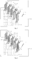
Fig. 1 schematically illustrates a structure resulting from a first step in a method for manufacturing a display device according to an embodiment of the present invention. -
Fig. 2 schematically illustrates a structure resulting from a third step in a method for manufacturing a display device according to an embodiment of the present invention. -
Fig. 3 schematically illustrates a structure resulting from a sixth step in a method for manufacturing a display device according to an embodiment of the present invention. -
Fig. 4 schematically illustrates a structure resulting from a contact hole fabrication process in a method for manufacturing a display device according to an embodiment of the present invention. -
Fig. 5 schematically illustrates a structure resulting from the patterning of a second conductive layer in a method for manufacturing a display device according to an embodiment of the present invention. - The present invention will be described in greater detail below with reference to specific embodiments which are to be read in conjunction with the accompanying drawings. Features and advantages of the invention will be more readily apparent from the following detailed description and from the drawings which are presented in a very simplified form not necessarily presented to scale, with the only intention to facilitate convenience and clarity in explaining the embodiments.
- With combined reference to
Figs. 1 to 5 , a method for manufacturing a display device according to the present invention includes the steps of: - 1) providing a
substrate 100; - 2) forming a polysilicon layer on the
substrate 100; - 3) patterning the polysilicon layer to form a plurality of
polysilicon blocks 110; - 4) implanting ions into the
polysilicon blocks 110; - 5) forming a gate insulating layer (not shown) over the plurality of
polysilicon blocks 110; - 6) forming a first conductive layer on the gate insulating layer; and
- 7) patterning the first conductive layer to form a plurality of
data lines 120, the plurality ofdata lines 120 partially overlapping thepolysilicon blocks 110 to provide compensating capacitors. - Specifically, first of all, as shown in
Fig. 1 , asubstrate 100 is provided. Thesubstrate 100 includes a display area and a non-display area surrounding the display area. The display area is formed with a pixel array including a plurality ofpixel cells 101 arranged in a pattern of array. Eachpixel cell 101 has a pixel capacitor and a thin film transistor (not shown). The non-display area is formed with a plurality ofGIP circuits 140 andtest circuits 150. - Subsequently, as shown in
Fig. 2 , a polysilicon layer is formed on thesubstrate 100 and patterned by an etching process to form a plurality of first plates (not shown) of the pixel capacitors in thepixel cells 101, sources and drains (not shown) of the thin film transistors in thepixel cells 101, and a plurality of polysilicon blocks 110 outside thepixel cells 101. In the embodiment illustrated inFig. 2 , thepolysilicon blocks 110 are formed between thepixel cells 101 and thetest circuits 150. Preferably, the polysilicon blocks 110 are all formed in the non-display area. - Next, boron or phosphorus ions are implanted into the first plates of the pixel capacitors and into the polysilicon blocks 110. The first plate and the
polysilicon block 110 are doped by ion implantation, the conductivity of the first plates andpolysilicon blocks 110 are improved. - After that, a gate insulating layer is formed over the patterned polysilicon layer and is then patterned.
- Thereafter, as shown in
Fig. 3 , a first conductive layer is formed over the patterned gate insulating layer and is then patterned by an etching process to form second plates (not shown) of the pixel capacitors, gates (not shown) of the thin film transistors and a plurality of data lines 120. Each of thedata lines 120 is connected to a corresponding one of thepixel cells 101 at one end and to a corresponding one of thetest circuits 150 at the other end. The data lines 120 partially overlap a corresponding one of the polysilicon blocks 110 to provide a compensating capacitor. - The compensating capacitor has a capacitance proportional to an overlapped area of the
data line 120 and thepolysilicon block 110. - In this embodiment, the overlapped area of the
data line 120 and thepolysilicon block 110 could be adjusted according to the number ofpixel cells 101 in connection with the correspondingdata line 120. Thefewer pixel cells 101 connected to thedata line 120 are, the smaller parasitic capacitance thedata line 120 will have, and hence the greater compensating capacitance will be required to be provided by the compensating capacitor, which corresponds to a greater overlapped area of thedata line 120 and thepolysilicon block 110. On the contrary, themore pixel cells 101 connected to thedata line 120 are, the larger a parasitic capacitance thedata line 120 will have, and hence the smaller a compensating capacitance will be required to be provided by the compensating capacitor, which corresponds to a smaller overlapped area of thedata line 120 and thepolysilicon block 110. - During the manufacturing process of the display device, for any of the
data lines 120, if it is designed to be connected to a relatively small number ofpixel cells 101, then an overlapped area of thedata line 120 and acorresponding polysilicon block 110 should be increased. On the contrary, if it is designed to be connected to a relatively large number ofpixel cells 101, then an overlapped area between thedata line 120 and acorresponding polysilicon block 110 has to be reduced. - Thereafter, as shown in
Fig. 4 , a contact hole fabrication process is performed to form a plurality ofcontact holes 110a in the polysilicon blocks 110. Thecontact holes 110a terminate within the polysilicon blocks 110, i.e., having a depth smaller than a thickness of the polysilicon blocks 110, so that the polysilicon blocks 110 are exposed at the bottoms of thecontact holes 110a. - Finally, as shown in
Fig. 5 , a second conductive layer is formed over the patterned first conductive layer and is then patterned by an etching process to formpower lines 131 and pixel connection lines 132. Thepower lines 131 are connected to the polysilicon blocks 110 via the contact holes 110a and thepixel connection lines 132 are configured to connect thepixel cells 101 to theGIP circuits 140. - According to the present invention, the materials of the first conductive layer and the second conductive layer are not limited to any particular materials and may be selected according to practical needs. Examples of the materials from which the first conductive layer and the second conductive layer are fabricated include transparent conductive materials such as indium tin oxide (ITO), indium zinc oxide (IZO), zirconium-doped zinc oxide (ZZO), fluorine-doped tin oxide (FTO), nano silver or the like and non-transparent conductive materials such as silver (Ag), aluminum (Al), tungsten, silver alloys, aluminum alloys or the like.
- In the resulting
display device 10, each of the compensating capacitors is constructed with one plate provided by the conductive layer and another plate provided by a polysilicon block. In traditional display devices, both of the plates of compensating capacitor are provided by conductive layers. - In the above method, since one plate of the compensating capacitor is provided by a
polysilicon block 110, the compensating capacitor has a reduced foot print and can be fabricated more easily. Moreover, the fabrication of the display device can be accomplished by using a two-metal process (involving the formation of two metal layers), dispensing with the need to employ a three-metal process (involving the formation of three metal layers). - In the present invention, a corresponding display device is provided. Further referring to
Fig. 5 , thedisplay device 10 includes asubstrate 100, a patterned polysilicon layer, a patterned gate insulating layer and a patterned first conductive layer stacked on thesubstrate 100 in sequence. The patterned polysilicon layer includes a plurality of polysilicon blocks 110. The patterned first conductive layer includes a plurality ofdata lines 120 each having a part overlapping a corresponding one of the polysilicon blocks 110 to form a compensating capacitor. - Specifically, the
display device 10 also includes a plurality of scan lines (not shown) for providing scan signals and a plurality ofdata lines 120 for providing data signals. The scan lines cross thedata lines 120 to form a plurality ofpixel cells 101 each arranged in an array. Each ofpixel cells 101 includes a pixel capacitor (not shown) and a thin film transistor (not shown). Second plates of the pixel capacitors and gates of the thin film transistors, together with data lines 120 (all located in the first conductive layer), are manufactured in the same process. First plates of the pixel capacitors and sources and drains of the thin film transistors and the polysilicon blocks 110 (all located in the polysilicon layer) are fabricated in the same process. - With continued reference to
Fig. 5 , the patterned polysilicon layer and the patterned first conductive layer are partially overlapped (i.e., thedata lines 120 partially overlapping with a corresponding one of the polysilicon blocks 110). The overlapped area of the polysilicon layer and the first conductive layer provides the opposing plates of the compensating capacitors, with the gate insulating layer between the polysilicon layer and the first conductive layer acting as the insulating dielectric of the compensating capacitor. - In this embodiment, the compensating capacitance is provided to compensate for parasitic capacitances of the data lines 120. The compensating capacitance of each of the compensating capacitors is proportional to an overlapped area of a corresponding one of the
data lines 120 and a corresponding one of the polysilicon blocks 110. The overlapped area of thedata line 120 and thepolysilicon block 110 is related to the number ofpixel cells 101 in connection with thedata line 120. Themore pixel cells 101 connected to thedata line 120 are, the smaller overlapped area of thedata line 120 and thepolysilicon block 110 is, and hence the compensating capacitance the compensating capacitor provides is smaller. On the contrary,fewer pixel cells 101 connected to thedata line 120, the greater the overlapped area of thedata line 120 and thepolysilicon block 110 is, and therefore the compensating capacitance provided by the compensating capacitor would be greater. - A data signal supplied to the
pixel cells 101 from thedata line 120 is also applied to one plate of the compensating capacitor, to compensate a parasitic capacitance compensation of thedata line 120. Since the compensating capacitances provided by the compensating capacitors depend on the numbers ofpixel cells 101 connected to thedata lines 120, the parasitic capacitance compensation for thedata lines 120 could be effectively achieved even if the number of pixel cells in different columns is different. Thus, display unevenness could be always avoided. - In conjunction with
Figs. 4 and5 , thedisplay device 10 further includes a plurality ofpower lines 131 connected at one end to thepixel cells 101 so as to provide the pixel cells with a power supply signal. Additionally, a plurality ofcontact holes 110a are provided in the polysilicon blocks 110. Thepower lines 131 are connected to the polysilicon blocks 110 via thecontact holes 110a. - Further referring to
Fig. 5 , thedisplay device 10 further includes a plurality ofpixel connection lines 132 andGIP circuits 140. Thepixel connection lines 132 connect thepixel cells 101 to theGIP circuits 140. In this embodiment, thepixel connection lines 132 and thepower lines 131 are fabricated (both in the second conductive layer) in the same process. - Further referring to
Fig. 5 , thedisplay device 10 further includestest circuits 150. The data lines 120 are connected at one end to thepixel cells 101 and to thetest circuits 150 at the other end. Thetest circuits 150 provide test signals for determining whether thedisplay device 10 displays images normally. - The display device in this embodiment could be a liquid crystal display (LCD) device, a plasma display panel (PDP), a vacuum fluorescent display (VFD) device, an organic light-emitting display (OLED) device, a flexible display device or a display device of another type, and the present application is not limited to any particular type of the display device.
- In summary, in the display device and the method of the present invention, the overlapped area between the doped polysilicon layer and the first conductive layer provides a compensating capacitor for the data line, so that the footprint of the compensating capacitor is reduced and hence the connection between the scan line and GIP circuit is facilitated.
- The description presented above is merely that of some preferred embodiments of the present invention and does not limit the scope thereof in any sense. Any and all changes and modifications made by those of ordinary skill in the art based on the above teachings fall within the scope as defined in the appended claims.
Claims (14)
- A display device, comprising:a substrate; anda patterned polysilicon layer, a patterned gate insulating layer and a patterned first conductive layer, stacked on the substrate in sequence, the patterned polysilicon layer comprising a plurality of polysilicon blocks doped with impurities, the patterned first conductive layer comprising a plurality of data lines, each of the plurality of data lines partially overlapping a corresponding polysilicon block of the plurality of polysilicon blocks to form a compensating capacitor.
- The display device of claim 1, further comprising a plurality of pixel cells each comprising a thin film transistor and a pixel capacitor, the patterned polysilicon layer further comprises a plurality of sources and drains of the thin film transistors of the plurality of pixel cells and a plurality of first plates of the pixel capacitors of the plurality of pixel cells, and the patterned first conductive layer further comprises gates of the thin film transistors of the plurality of pixel cells and a plurality of second plates of the pixel capacitors of the plurality of pixel cells.
- The display device of claim 2, further comprising a plurality of test circuits, wherein each of the data lines has a first end connected to a corresponding pixel cell of the plurality of pixel cells and a second end connected to a corresponding test circuit of the plurality of test circuits.
- The display device of claim 2, further comprising a plurality of GIP circuits, a plurality of pixel connection lines and a plurality of power lines, the plurality of pixel connection lines and power lines being situated in a same layer and made of a same material, the plurality of power lines being connected to the plurality of pixel cells to provide the plurality of pixel cells with a power supply signal, the plurality of pixel connection lines connecting the plurality of pixel cells to the plurality of GIP circuits.
- The display device of claim 1, wherein the compensating capacitor is provided to compensate for a parasitic capacitance of the data line, and a compensating capacitance of the compensating capacitor is proportional to an overlapped area of the data line and the polysilicon block.
- The display device of claim 5, wherein the overlapped area of the data line and the polysilicon block is related to a number of the pixel cells connected to the data line.
- A method for manufacturing a display device, comprising:providing a substrate;forming a polysilicon layer on the substrate;patterning the polysilicon layer to form a plurality of polysilicon blocks;implanting ions into the plurality of polysilicon blocks;forming a gate insulating layer over the plurality of polysilicon blocks;forming a first conductive layer on the gate insulating layer; andpatterning the first conductive layer to form a plurality of data lines, each of plurality of data lines partially overlapping a corresponding polysilicon block of the polysilicon blocks to form a compensating capacitor.
- The method for manufacturing a display device of claim 7, further comprising, during the patterning the polysilicon layer to form a plurality of polysilicon blocks, patterning the polysilicon layer to form a plurality of first plates of a plurality of pixel capacitors and a plurality of sources and drains of a plurality of thin film transistors.
- The method for manufacturing a display device of claim 8, further comprising, during the implanting ions into the plurality of polysilicon blocks, implanting ions into the first plates of the plurality of pixel capacitors.
- The method for manufacturing a display device of claim 8, further comprising, during patterning the first conductive layer to form a plurality of data lines, patterning the first conductive layer to form a plurality of second plates of the plurality of pixel capacitors and a plurality of gates of the plurality of thin film transistors.
- The method for manufacturing a display device of claim 7, further comprising, subsequent to the patterning the first conductive layer to form a plurality of data lines, forming a second conductive layer over the patterned first conductive layer and patterning the second conductive layer to form a plurality of pixel connection lines and a plurality of power lines.
- The method for manufacturing a display device of claim 11, further comprising, prior to the forming a second conductive layer over the patterned first conductive layer and subsequent to the patterning the first conductive layer to form the plurality of data lines, forming a plurality of contact holes in the polysilicon blocks for connecting the power lines to the polysilicon blocks.
- The method for manufacturing a display device of claim 7, wherein an overlapped area of the data line and the polysilicon block is determined by a number of pixel cells connected to the data line.
- The method for manufacturing a display device of claim 13, wherein the overlapped area of the data line and the polysilicon block is inversely related to the number of pixel cells connected to the data line.
Applications Claiming Priority (2)
| Application Number | Priority Date | Filing Date | Title |
|---|---|---|---|
| CN201611147363.3A CN108231790B (en) | 2016-12-13 | 2016-12-13 | Display device and its manufacturing method |
| PCT/CN2017/115604 WO2018108069A1 (en) | 2016-12-13 | 2017-12-12 | Display device and manufacturing method therefor |
Publications (3)
| Publication Number | Publication Date |
|---|---|
| EP3528286A1 true EP3528286A1 (en) | 2019-08-21 |
| EP3528286A4 EP3528286A4 (en) | 2019-11-27 |
| EP3528286B1 EP3528286B1 (en) | 2024-03-27 |
Family
ID=62557951
Family Applications (1)
| Application Number | Title | Priority Date | Filing Date |
|---|---|---|---|
| EP17881307.7A Active EP3528286B1 (en) | 2016-12-13 | 2017-12-12 | Display device and manufacturing method therefor |
Country Status (7)
| Country | Link |
|---|---|
| US (1) | US10797089B2 (en) |
| EP (1) | EP3528286B1 (en) |
| JP (1) | JP6758427B2 (en) |
| KR (1) | KR102174662B1 (en) |
| CN (1) | CN108231790B (en) |
| TW (1) | TWI663718B (en) |
| WO (1) | WO2018108069A1 (en) |
Families Citing this family (4)
| Publication number | Priority date | Publication date | Assignee | Title |
|---|---|---|---|---|
| CN109523963B (en) | 2018-11-21 | 2020-10-16 | 惠科股份有限公司 | Display device's drive circuit and display device |
| CN111123597B (en) * | 2020-01-11 | 2025-09-23 | 鸿富锦精密工业(深圳)有限公司 | Array substrate, display panel and display device |
| CN114464644B (en) * | 2020-11-09 | 2025-03-21 | 京东方科技集团股份有限公司 | Display substrate and display device |
| KR20220140093A (en) | 2021-04-08 | 2022-10-18 | 삼성디스플레이 주식회사 | Display apparatus |
Family Cites Families (29)
| Publication number | Priority date | Publication date | Assignee | Title |
|---|---|---|---|---|
| JP4096585B2 (en) | 2001-03-19 | 2008-06-04 | セイコーエプソン株式会社 | Display device manufacturing method, display device, and electronic apparatus |
| KR100831235B1 (en) | 2002-06-07 | 2008-05-22 | 삼성전자주식회사 | Thin film transistor substrate |
| KR20060041949A (en) | 2004-04-15 | 2006-05-12 | 미쓰비시덴키 가부시키가이샤 | Driving circuit having offset compensation function and liquid crystal display device using the same |
| KR100662989B1 (en) * | 2004-08-20 | 2006-12-28 | 삼성에스디아이 주식회사 | Display device having an inspection circuit |
| KR100647774B1 (en) | 2004-11-04 | 2006-11-23 | 엘지.필립스 엘시디 주식회사 | Polysilicon Thin Film Transistor Substrate and Manufacturing Method |
| CN101536064B (en) | 2006-11-21 | 2011-06-15 | 夏普株式会社 | Active matrix substrate, display panel, and display |
| CN101286515A (en) | 2007-04-13 | 2008-10-15 | 群康科技(深圳)有限公司 | Thin film transistor substrate and manufacturing method thereof |
| CN101779227B (en) | 2007-10-24 | 2012-03-28 | 夏普株式会社 | Display panel and display |
| JP2010249955A (en) * | 2009-04-13 | 2010-11-04 | Global Oled Technology Llc | Display device |
| KR101736319B1 (en) * | 2010-12-14 | 2017-05-17 | 삼성디스플레이 주식회사 | Organic light emitting display device and manufacturing method of the same |
| KR101825643B1 (en) * | 2011-01-10 | 2018-02-06 | 삼성디스플레이 주식회사 | Organic light emitting display device |
| CN102368499B (en) * | 2011-10-27 | 2014-04-16 | 深圳市华星光电技术有限公司 | TFT array substrate and liquid crystal panel |
| JP5997958B2 (en) | 2012-07-23 | 2016-09-28 | 株式会社ジャパンディスプレイ | Display device and array substrate |
| CN103296030B (en) * | 2012-07-25 | 2015-12-09 | 上海天马微电子有限公司 | TFT-LCD array substrate |
| JP6196456B2 (en) * | 2013-04-01 | 2017-09-13 | シナプティクス・ジャパン合同会社 | Display device and source driver IC |
| CN103325688A (en) | 2013-06-17 | 2013-09-25 | 深圳市华星光电技术有限公司 | Method for forming channel of thin film transistor and compensating circuit |
| CN103915431B (en) | 2013-06-17 | 2017-10-20 | 上海天马微电子有限公司 | TFT array substrate, display device and array substrate manufacturing method |
| US9190005B2 (en) * | 2014-03-05 | 2015-11-17 | Innolux Corporation | Display panel |
| JP2015227974A (en) * | 2014-06-02 | 2015-12-17 | 株式会社ジャパンディスプレイ | Display device |
| CN104064601B (en) | 2014-06-30 | 2017-12-26 | 上海天马微电子有限公司 | TFT, TFT array substrate, manufacturing method of TFT array substrate, display panel and display device |
| US10283040B2 (en) * | 2015-02-03 | 2019-05-07 | Sharp Kabushiki Kaisha | Data signal line drive circuit, data signal line drive method and display device |
| KR102293411B1 (en) * | 2015-05-08 | 2021-08-25 | 삼성디스플레이 주식회사 | Nonsquare display |
| KR102507151B1 (en) * | 2015-08-27 | 2023-03-08 | 티씨엘 차이나 스타 옵토일렉트로닉스 테크놀로지 컴퍼니 리미티드 | Display device and manufacturing method thereof |
| KR20170028464A (en) * | 2015-09-03 | 2017-03-14 | 삼성디스플레이 주식회사 | Display apparatus |
| CN105204248A (en) | 2015-10-10 | 2015-12-30 | 重庆京东方光电科技有限公司 | Array substrate and display device |
| CN105513528B (en) | 2016-02-04 | 2018-06-22 | 京东方科技集团股份有限公司 | Capacitor compensating circuit, display base plate, display device and capacitance compensation method |
| KR102503164B1 (en) * | 2016-04-05 | 2023-02-24 | 삼성디스플레이 주식회사 | Display panel and method of manufacturing the same |
| CN106449651B (en) * | 2016-09-12 | 2019-05-21 | 厦门天马微电子有限公司 | Dot structure and display device |
| KR102430809B1 (en) * | 2017-09-29 | 2022-08-09 | 엘지디스플레이 주식회사 | Double sided display |
-
2016
- 2016-12-13 CN CN201611147363.3A patent/CN108231790B/en active Active
-
2017
- 2017-12-12 EP EP17881307.7A patent/EP3528286B1/en active Active
- 2017-12-12 US US16/313,619 patent/US10797089B2/en active Active
- 2017-12-12 WO PCT/CN2017/115604 patent/WO2018108069A1/en not_active Ceased
- 2017-12-12 JP JP2018567934A patent/JP6758427B2/en active Active
- 2017-12-12 KR KR1020197012509A patent/KR102174662B1/en active Active
- 2017-12-13 TW TW106143757A patent/TWI663718B/en active
Also Published As
| Publication number | Publication date |
|---|---|
| WO2018108069A1 (en) | 2018-06-21 |
| US10797089B2 (en) | 2020-10-06 |
| JP2020500321A (en) | 2020-01-09 |
| CN108231790B (en) | 2019-09-17 |
| KR20190054172A (en) | 2019-05-21 |
| CN108231790A (en) | 2018-06-29 |
| US20190326334A1 (en) | 2019-10-24 |
| JP6758427B2 (en) | 2020-09-23 |
| TWI663718B (en) | 2019-06-21 |
| KR102174662B1 (en) | 2020-11-05 |
| EP3528286A4 (en) | 2019-11-27 |
| TW201838159A (en) | 2018-10-16 |
| EP3528286B1 (en) | 2024-03-27 |
Similar Documents
| Publication | Publication Date | Title |
|---|---|---|
| US10042495B2 (en) | Touch display panel, manufacturing method thereof, driving method thereof and touch display device | |
| US10665644B2 (en) | Organic light emitting display panel and fabricating method thereof, display device | |
| US10254876B2 (en) | Array substrate, fabricating method thereof and display device | |
| CN103293811B (en) | A kind of array base palte and preparation method thereof, display unit | |
| US9117679B2 (en) | Organic light emitting diode, touch display device and method for fabricating the same | |
| EP3664138B1 (en) | Wiring structure and preparation method therefor, oled array substrate and display device | |
| US20160372490A1 (en) | Array substrate and manufacturing method thereof, and display panel | |
| CN104393021A (en) | Pixel structure, transparent touch screen and preparation method and display device therefore | |
| EP2991121B1 (en) | Array substrate, method for manufacturing array substrate and display device | |
| US10797089B2 (en) | Display device having compensating capacitor and method of manufacturing the same | |
| JP2004110034A (en) | Display device substrate, liquid crystal display device, and method of manufacturing liquid crystal display device | |
| CN105068373A (en) | Manufacturing method of TFT (Thin Film Transistor) substrate structure | |
| TW201013279A (en) | Liquid crystal display and method of manufacturing the same | |
| US20220238614A1 (en) | Display substrates and manufacturing methods thereof, and display devices | |
| WO2017049842A1 (en) | Array substrate, manufacturing method thereof, and display device | |
| TW201401522A (en) | Thin film transistor substrate containing MOS and manufacturing method thereof | |
| US20140346511A1 (en) | Array substrate, manufacturing method, and display device thereof | |
| CN100394295C (en) | Thin-film semiconductor device and manufacturing method thereof, electro-optic device and electronic equipment | |
| CN103681692A (en) | Array substrate, production method thereof and display device | |
| CN113380863B (en) | Display panel and electronic device | |
| US6757033B2 (en) | Liquid crystal display device and method for manufacturing the same | |
| JP2003332041A (en) | Electro-optical devices and electronic equipment | |
| KR102037514B1 (en) | Thin Film Transistor Panel For Flat Panel Display Device And Method For Manufacturing The Same | |
| US20160370671A1 (en) | Array substrate, manufacturing method thereof, and display device | |
| CN108400140B (en) | Array substrate and manufacturing method thereof |
Legal Events
| Date | Code | Title | Description |
|---|---|---|---|
| STAA | Information on the status of an ep patent application or granted ep patent |
Free format text: STATUS: THE INTERNATIONAL PUBLICATION HAS BEEN MADE |
|
| PUAI | Public reference made under article 153(3) epc to a published international application that has entered the european phase |
Free format text: ORIGINAL CODE: 0009012 |
|
| STAA | Information on the status of an ep patent application or granted ep patent |
Free format text: STATUS: REQUEST FOR EXAMINATION WAS MADE |
|
| 17P | Request for examination filed |
Effective date: 20190430 |
|
| AK | Designated contracting states |
Kind code of ref document: A1 Designated state(s): AL AT BE BG CH CY CZ DE DK EE ES FI FR GB GR HR HU IE IS IT LI LT LU LV MC MK MT NL NO PL PT RO RS SE SI SK SM TR |
|
| AX | Request for extension of the european patent |
Extension state: BA ME |
|
| A4 | Supplementary search report drawn up and despatched |
Effective date: 20191028 |
|
| RIC1 | Information provided on ipc code assigned before grant |
Ipc: G09G 3/36 20060101ALI20191022BHEP Ipc: H01L 27/12 20060101AFI20191022BHEP |
|
| DAV | Request for validation of the european patent (deleted) | ||
| DAX | Request for extension of the european patent (deleted) | ||
| STAA | Information on the status of an ep patent application or granted ep patent |
Free format text: STATUS: EXAMINATION IS IN PROGRESS |
|
| 17Q | First examination report despatched |
Effective date: 20211013 |
|
| GRAP | Despatch of communication of intention to grant a patent |
Free format text: ORIGINAL CODE: EPIDOSNIGR1 |
|
| STAA | Information on the status of an ep patent application or granted ep patent |
Free format text: STATUS: GRANT OF PATENT IS INTENDED |
|
| RIC1 | Information provided on ipc code assigned before grant |
Ipc: G09G 3/36 20060101ALI20231108BHEP Ipc: G09G 3/20 20060101ALI20231108BHEP Ipc: H01L 27/12 20060101AFI20231108BHEP |
|
| INTG | Intention to grant announced |
Effective date: 20231212 |
|
| GRAS | Grant fee paid |
Free format text: ORIGINAL CODE: EPIDOSNIGR3 |
|
| GRAA | (expected) grant |
Free format text: ORIGINAL CODE: 0009210 |
|
| STAA | Information on the status of an ep patent application or granted ep patent |
Free format text: STATUS: THE PATENT HAS BEEN GRANTED |
|
| AK | Designated contracting states |
Kind code of ref document: B1 Designated state(s): AL AT BE BG CH CY CZ DE DK EE ES FI FR GB GR HR HU IE IS IT LI LT LU LV MC MK MT NL NO PL PT RO RS SE SI SK SM TR |
|
| REG | Reference to a national code |
Ref country code: GB Ref legal event code: FG4D |
|
| REG | Reference to a national code |
Ref country code: CH Ref legal event code: EP |
|
| REG | Reference to a national code |
Ref country code: DE Ref legal event code: R096 Ref document number: 602017080479 Country of ref document: DE |
|
| REG | Reference to a national code |
Ref country code: IE Ref legal event code: FG4D |
|
| PG25 | Lapsed in a contracting state [announced via postgrant information from national office to epo] |
Ref country code: LT Free format text: LAPSE BECAUSE OF FAILURE TO SUBMIT A TRANSLATION OF THE DESCRIPTION OR TO PAY THE FEE WITHIN THE PRESCRIBED TIME-LIMIT Effective date: 20240327 |
|
| REG | Reference to a national code |
Ref country code: LT Ref legal event code: MG9D |
|
| PG25 | Lapsed in a contracting state [announced via postgrant information from national office to epo] |
Ref country code: GR Free format text: LAPSE BECAUSE OF FAILURE TO SUBMIT A TRANSLATION OF THE DESCRIPTION OR TO PAY THE FEE WITHIN THE PRESCRIBED TIME-LIMIT Effective date: 20240628 |
|
| PG25 | Lapsed in a contracting state [announced via postgrant information from national office to epo] |
Ref country code: HR Free format text: LAPSE BECAUSE OF FAILURE TO SUBMIT A TRANSLATION OF THE DESCRIPTION OR TO PAY THE FEE WITHIN THE PRESCRIBED TIME-LIMIT Effective date: 20240327 Ref country code: RS Free format text: LAPSE BECAUSE OF FAILURE TO SUBMIT A TRANSLATION OF THE DESCRIPTION OR TO PAY THE FEE WITHIN THE PRESCRIBED TIME-LIMIT Effective date: 20240627 |
|
| PG25 | Lapsed in a contracting state [announced via postgrant information from national office to epo] |
Ref country code: RS Free format text: LAPSE BECAUSE OF FAILURE TO SUBMIT A TRANSLATION OF THE DESCRIPTION OR TO PAY THE FEE WITHIN THE PRESCRIBED TIME-LIMIT Effective date: 20240627 Ref country code: NO Free format text: LAPSE BECAUSE OF FAILURE TO SUBMIT A TRANSLATION OF THE DESCRIPTION OR TO PAY THE FEE WITHIN THE PRESCRIBED TIME-LIMIT Effective date: 20240627 Ref country code: LT Free format text: LAPSE BECAUSE OF FAILURE TO SUBMIT A TRANSLATION OF THE DESCRIPTION OR TO PAY THE FEE WITHIN THE PRESCRIBED TIME-LIMIT Effective date: 20240327 Ref country code: HR Free format text: LAPSE BECAUSE OF FAILURE TO SUBMIT A TRANSLATION OF THE DESCRIPTION OR TO PAY THE FEE WITHIN THE PRESCRIBED TIME-LIMIT Effective date: 20240327 Ref country code: GR Free format text: LAPSE BECAUSE OF FAILURE TO SUBMIT A TRANSLATION OF THE DESCRIPTION OR TO PAY THE FEE WITHIN THE PRESCRIBED TIME-LIMIT Effective date: 20240628 Ref country code: FI Free format text: LAPSE BECAUSE OF FAILURE TO SUBMIT A TRANSLATION OF THE DESCRIPTION OR TO PAY THE FEE WITHIN THE PRESCRIBED TIME-LIMIT Effective date: 20240327 Ref country code: BG Free format text: LAPSE BECAUSE OF FAILURE TO SUBMIT A TRANSLATION OF THE DESCRIPTION OR TO PAY THE FEE WITHIN THE PRESCRIBED TIME-LIMIT Effective date: 20240327 |
|
| REG | Reference to a national code |
Ref country code: NL Ref legal event code: MP Effective date: 20240327 |
|
| PG25 | Lapsed in a contracting state [announced via postgrant information from national office to epo] |
Ref country code: SE Free format text: LAPSE BECAUSE OF FAILURE TO SUBMIT A TRANSLATION OF THE DESCRIPTION OR TO PAY THE FEE WITHIN THE PRESCRIBED TIME-LIMIT Effective date: 20240327 Ref country code: LV Free format text: LAPSE BECAUSE OF FAILURE TO SUBMIT A TRANSLATION OF THE DESCRIPTION OR TO PAY THE FEE WITHIN THE PRESCRIBED TIME-LIMIT Effective date: 20240327 |
|
| PG25 | Lapsed in a contracting state [announced via postgrant information from national office to epo] |
Ref country code: NL Free format text: LAPSE BECAUSE OF FAILURE TO SUBMIT A TRANSLATION OF THE DESCRIPTION OR TO PAY THE FEE WITHIN THE PRESCRIBED TIME-LIMIT Effective date: 20240327 |
|
| REG | Reference to a national code |
Ref country code: AT Ref legal event code: MK05 Ref document number: 1670759 Country of ref document: AT Kind code of ref document: T Effective date: 20240327 |
|
| PG25 | Lapsed in a contracting state [announced via postgrant information from national office to epo] |
Ref country code: NL Free format text: LAPSE BECAUSE OF FAILURE TO SUBMIT A TRANSLATION OF THE DESCRIPTION OR TO PAY THE FEE WITHIN THE PRESCRIBED TIME-LIMIT Effective date: 20240327 |
|
| PG25 | Lapsed in a contracting state [announced via postgrant information from national office to epo] |
Ref country code: IS Free format text: LAPSE BECAUSE OF FAILURE TO SUBMIT A TRANSLATION OF THE DESCRIPTION OR TO PAY THE FEE WITHIN THE PRESCRIBED TIME-LIMIT Effective date: 20240727 |
|
| PG25 | Lapsed in a contracting state [announced via postgrant information from national office to epo] |
Ref country code: SM Free format text: LAPSE BECAUSE OF FAILURE TO SUBMIT A TRANSLATION OF THE DESCRIPTION OR TO PAY THE FEE WITHIN THE PRESCRIBED TIME-LIMIT Effective date: 20240327 Ref country code: PT Free format text: LAPSE BECAUSE OF FAILURE TO SUBMIT A TRANSLATION OF THE DESCRIPTION OR TO PAY THE FEE WITHIN THE PRESCRIBED TIME-LIMIT Effective date: 20240729 |
|
| PG25 | Lapsed in a contracting state [announced via postgrant information from national office to epo] |
Ref country code: ES Free format text: LAPSE BECAUSE OF FAILURE TO SUBMIT A TRANSLATION OF THE DESCRIPTION OR TO PAY THE FEE WITHIN THE PRESCRIBED TIME-LIMIT Effective date: 20240327 |
|
| PG25 | Lapsed in a contracting state [announced via postgrant information from national office to epo] |
Ref country code: CZ Free format text: LAPSE BECAUSE OF FAILURE TO SUBMIT A TRANSLATION OF THE DESCRIPTION OR TO PAY THE FEE WITHIN THE PRESCRIBED TIME-LIMIT Effective date: 20240327 Ref country code: EE Free format text: LAPSE BECAUSE OF FAILURE TO SUBMIT A TRANSLATION OF THE DESCRIPTION OR TO PAY THE FEE WITHIN THE PRESCRIBED TIME-LIMIT Effective date: 20240327 |
|
| PG25 | Lapsed in a contracting state [announced via postgrant information from national office to epo] |
Ref country code: AT Free format text: LAPSE BECAUSE OF FAILURE TO SUBMIT A TRANSLATION OF THE DESCRIPTION OR TO PAY THE FEE WITHIN THE PRESCRIBED TIME-LIMIT Effective date: 20240327 |
|
| PG25 | Lapsed in a contracting state [announced via postgrant information from national office to epo] |
Ref country code: PL Free format text: LAPSE BECAUSE OF FAILURE TO SUBMIT A TRANSLATION OF THE DESCRIPTION OR TO PAY THE FEE WITHIN THE PRESCRIBED TIME-LIMIT Effective date: 20240327 |
|
| PG25 | Lapsed in a contracting state [announced via postgrant information from national office to epo] |
Ref country code: SK Free format text: LAPSE BECAUSE OF FAILURE TO SUBMIT A TRANSLATION OF THE DESCRIPTION OR TO PAY THE FEE WITHIN THE PRESCRIBED TIME-LIMIT Effective date: 20240327 |
|
| PG25 | Lapsed in a contracting state [announced via postgrant information from national office to epo] |
Ref country code: SM Free format text: LAPSE BECAUSE OF FAILURE TO SUBMIT A TRANSLATION OF THE DESCRIPTION OR TO PAY THE FEE WITHIN THE PRESCRIBED TIME-LIMIT Effective date: 20240327 Ref country code: SK Free format text: LAPSE BECAUSE OF FAILURE TO SUBMIT A TRANSLATION OF THE DESCRIPTION OR TO PAY THE FEE WITHIN THE PRESCRIBED TIME-LIMIT Effective date: 20240327 Ref country code: RO Free format text: LAPSE BECAUSE OF FAILURE TO SUBMIT A TRANSLATION OF THE DESCRIPTION OR TO PAY THE FEE WITHIN THE PRESCRIBED TIME-LIMIT Effective date: 20240327 Ref country code: PT Free format text: LAPSE BECAUSE OF FAILURE TO SUBMIT A TRANSLATION OF THE DESCRIPTION OR TO PAY THE FEE WITHIN THE PRESCRIBED TIME-LIMIT Effective date: 20240729 Ref country code: PL Free format text: LAPSE BECAUSE OF FAILURE TO SUBMIT A TRANSLATION OF THE DESCRIPTION OR TO PAY THE FEE WITHIN THE PRESCRIBED TIME-LIMIT Effective date: 20240327 Ref country code: IS Free format text: LAPSE BECAUSE OF FAILURE TO SUBMIT A TRANSLATION OF THE DESCRIPTION OR TO PAY THE FEE WITHIN THE PRESCRIBED TIME-LIMIT Effective date: 20240727 Ref country code: ES Free format text: LAPSE BECAUSE OF FAILURE TO SUBMIT A TRANSLATION OF THE DESCRIPTION OR TO PAY THE FEE WITHIN THE PRESCRIBED TIME-LIMIT Effective date: 20240327 Ref country code: EE Free format text: LAPSE BECAUSE OF FAILURE TO SUBMIT A TRANSLATION OF THE DESCRIPTION OR TO PAY THE FEE WITHIN THE PRESCRIBED TIME-LIMIT Effective date: 20240327 Ref country code: CZ Free format text: LAPSE BECAUSE OF FAILURE TO SUBMIT A TRANSLATION OF THE DESCRIPTION OR TO PAY THE FEE WITHIN THE PRESCRIBED TIME-LIMIT Effective date: 20240327 Ref country code: AT Free format text: LAPSE BECAUSE OF FAILURE TO SUBMIT A TRANSLATION OF THE DESCRIPTION OR TO PAY THE FEE WITHIN THE PRESCRIBED TIME-LIMIT Effective date: 20240327 |
|
| REG | Reference to a national code |
Ref country code: DE Ref legal event code: R079 Ref document number: 602017080479 Country of ref document: DE Free format text: PREVIOUS MAIN CLASS: H01L0027120000 Ipc: H10D0086000000 |
|
| PG25 | Lapsed in a contracting state [announced via postgrant information from national office to epo] |
Ref country code: IT Free format text: LAPSE BECAUSE OF FAILURE TO SUBMIT A TRANSLATION OF THE DESCRIPTION OR TO PAY THE FEE WITHIN THE PRESCRIBED TIME-LIMIT Effective date: 20240327 |
|
| PG25 | Lapsed in a contracting state [announced via postgrant information from national office to epo] |
Ref country code: IT Free format text: LAPSE BECAUSE OF FAILURE TO SUBMIT A TRANSLATION OF THE DESCRIPTION OR TO PAY THE FEE WITHIN THE PRESCRIBED TIME-LIMIT Effective date: 20240327 |
|
| REG | Reference to a national code |
Ref country code: DE Ref legal event code: R097 Ref document number: 602017080479 Country of ref document: DE |
|
| PG25 | Lapsed in a contracting state [announced via postgrant information from national office to epo] |
Ref country code: DK Free format text: LAPSE BECAUSE OF FAILURE TO SUBMIT A TRANSLATION OF THE DESCRIPTION OR TO PAY THE FEE WITHIN THE PRESCRIBED TIME-LIMIT Effective date: 20240327 |
|
| PG25 | Lapsed in a contracting state [announced via postgrant information from national office to epo] |
Ref country code: DK Free format text: LAPSE BECAUSE OF FAILURE TO SUBMIT A TRANSLATION OF THE DESCRIPTION OR TO PAY THE FEE WITHIN THE PRESCRIBED TIME-LIMIT Effective date: 20240327 |
|
| PLBE | No opposition filed within time limit |
Free format text: ORIGINAL CODE: 0009261 |
|
| STAA | Information on the status of an ep patent application or granted ep patent |
Free format text: STATUS: NO OPPOSITION FILED WITHIN TIME LIMIT |
|
| 26N | No opposition filed |
Effective date: 20250103 |
|
| PG25 | Lapsed in a contracting state [announced via postgrant information from national office to epo] |
Ref country code: SI Free format text: LAPSE BECAUSE OF FAILURE TO SUBMIT A TRANSLATION OF THE DESCRIPTION OR TO PAY THE FEE WITHIN THE PRESCRIBED TIME-LIMIT Effective date: 20240327 |
|
| PG25 | Lapsed in a contracting state [announced via postgrant information from national office to epo] |
Ref country code: MC Free format text: LAPSE BECAUSE OF FAILURE TO SUBMIT A TRANSLATION OF THE DESCRIPTION OR TO PAY THE FEE WITHIN THE PRESCRIBED TIME-LIMIT Effective date: 20240327 |
|
| REG | Reference to a national code |
Ref country code: CH Ref legal event code: PL |
|
| PG25 | Lapsed in a contracting state [announced via postgrant information from national office to epo] |
Ref country code: LU Free format text: LAPSE BECAUSE OF NON-PAYMENT OF DUE FEES Effective date: 20241212 |
|
| REG | Reference to a national code |
Ref country code: BE Ref legal event code: MM Effective date: 20241231 |
|
| PG25 | Lapsed in a contracting state [announced via postgrant information from national office to epo] |
Ref country code: BE Free format text: LAPSE BECAUSE OF NON-PAYMENT OF DUE FEES Effective date: 20241231 |
|
| PG25 | Lapsed in a contracting state [announced via postgrant information from national office to epo] |
Ref country code: CH Free format text: LAPSE BECAUSE OF NON-PAYMENT OF DUE FEES Effective date: 20241231 |
|
| PG25 | Lapsed in a contracting state [announced via postgrant information from national office to epo] |
Ref country code: IE Free format text: LAPSE BECAUSE OF NON-PAYMENT OF DUE FEES Effective date: 20241212 |
|
| PGFP | Annual fee paid to national office [announced via postgrant information from national office to epo] |
Ref country code: GB Payment date: 20251229 Year of fee payment: 9 |
|
| PGFP | Annual fee paid to national office [announced via postgrant information from national office to epo] |
Ref country code: FR Payment date: 20251230 Year of fee payment: 9 |
|
| PGFP | Annual fee paid to national office [announced via postgrant information from national office to epo] |
Ref country code: DE Payment date: 20251231 Year of fee payment: 9 |