EP3527564A1 - Novel heterocyclic compound and organic light emitting element using same - Google Patents
Novel heterocyclic compound and organic light emitting element using same Download PDFInfo
- Publication number
- EP3527564A1 EP3527564A1 EP18741013.9A EP18741013A EP3527564A1 EP 3527564 A1 EP3527564 A1 EP 3527564A1 EP 18741013 A EP18741013 A EP 18741013A EP 3527564 A1 EP3527564 A1 EP 3527564A1
- Authority
- EP
- European Patent Office
- Prior art keywords
- group
- light emitting
- layer
- formula
- compound
- Prior art date
- Legal status (The legal status is an assumption and is not a legal conclusion. Google has not performed a legal analysis and makes no representation as to the accuracy of the status listed.)
- Granted
Links
- 150000002391 heterocyclic compounds Chemical class 0.000 title description 4
- 150000001875 compounds Chemical class 0.000 claims description 102
- -1 cyano, biphenylyl Chemical group 0.000 claims description 54
- 239000011368 organic material Substances 0.000 claims description 41
- 238000002347 injection Methods 0.000 claims description 39
- 239000007924 injection Substances 0.000 claims description 39
- 125000003118 aryl group Chemical group 0.000 claims description 25
- 229910052760 oxygen Inorganic materials 0.000 claims description 13
- 125000004093 cyano group Chemical group *C#N 0.000 claims description 10
- 229910052717 sulfur Inorganic materials 0.000 claims description 10
- 125000001997 phenyl group Chemical group [H]C1=C([H])C([H])=C(*)C([H])=C1[H] 0.000 claims description 5
- 125000000732 arylene group Chemical group 0.000 claims description 4
- 125000005549 heteroarylene group Chemical group 0.000 claims description 4
- 125000006819 (C2-60) heteroaryl group Chemical group 0.000 claims description 3
- 150000001923 cyclic compounds Chemical class 0.000 abstract 1
- 239000010410 layer Substances 0.000 description 124
- 238000006243 chemical reaction Methods 0.000 description 37
- 239000000463 material Substances 0.000 description 30
- 230000032258 transport Effects 0.000 description 28
- 239000007858 starting material Substances 0.000 description 27
- 125000004432 carbon atom Chemical group C* 0.000 description 21
- 230000000052 comparative effect Effects 0.000 description 18
- 230000005525 hole transport Effects 0.000 description 14
- 125000001424 substituent group Chemical group 0.000 description 14
- 239000000758 substrate Substances 0.000 description 14
- TXCDCPKCNAJMEE-UHFFFAOYSA-N dibenzofuran Chemical compound C1=CC=C2C3=CC=CC=C3OC2=C1 TXCDCPKCNAJMEE-UHFFFAOYSA-N 0.000 description 10
- IYYZUPMFVPLQIF-UHFFFAOYSA-N dibenzothiophene Chemical compound C1=CC=C2C3=CC=CC=C3SC2=C1 IYYZUPMFVPLQIF-UHFFFAOYSA-N 0.000 description 10
- 125000000217 alkyl group Chemical group 0.000 description 9
- 125000000623 heterocyclic group Chemical group 0.000 description 9
- 229910052782 aluminium Inorganic materials 0.000 description 8
- XAGFODPZIPBFFR-UHFFFAOYSA-N aluminium Chemical compound [Al] XAGFODPZIPBFFR-UHFFFAOYSA-N 0.000 description 8
- BWHMMNNQKKPAPP-UHFFFAOYSA-L potassium carbonate Chemical compound [K+].[K+].[O-]C([O-])=O BWHMMNNQKKPAPP-UHFFFAOYSA-L 0.000 description 8
- XLYOFNOQVPJJNP-UHFFFAOYSA-N water Substances O XLYOFNOQVPJJNP-UHFFFAOYSA-N 0.000 description 8
- 125000003342 alkenyl group Chemical group 0.000 description 7
- 125000000753 cycloalkyl group Chemical group 0.000 description 7
- 238000000034 method Methods 0.000 description 7
- 239000007787 solid Substances 0.000 description 7
- XEKOWRVHYACXOJ-UHFFFAOYSA-N Ethyl acetate Chemical compound CCOC(C)=O XEKOWRVHYACXOJ-UHFFFAOYSA-N 0.000 description 6
- 239000010406 cathode material Substances 0.000 description 6
- 239000010405 anode material Substances 0.000 description 5
- 150000004982 aromatic amines Chemical class 0.000 description 5
- 230000000694 effects Effects 0.000 description 5
- PQXKHYXIUOZZFA-UHFFFAOYSA-M lithium fluoride Chemical compound [Li+].[F-] PQXKHYXIUOZZFA-UHFFFAOYSA-M 0.000 description 5
- 229910052751 metal Inorganic materials 0.000 description 5
- 239000002184 metal Substances 0.000 description 5
- JYEUMXHLPRZUAT-UHFFFAOYSA-N 1,2,3-triazine Chemical group C1=CN=NN=C1 JYEUMXHLPRZUAT-UHFFFAOYSA-N 0.000 description 4
- LFQSCWFLJHTTHZ-UHFFFAOYSA-N Ethanol Chemical compound CCO LFQSCWFLJHTTHZ-UHFFFAOYSA-N 0.000 description 4
- 238000000151 deposition Methods 0.000 description 4
- 239000012153 distilled water Substances 0.000 description 4
- 125000004185 ester group Chemical group 0.000 description 4
- 125000001072 heteroaryl group Chemical group 0.000 description 4
- 238000004770 highest occupied molecular orbital Methods 0.000 description 4
- 229910000027 potassium carbonate Inorganic materials 0.000 description 4
- TYJJADVDDVDEDZ-UHFFFAOYSA-M potassium hydrogencarbonate Chemical compound [K+].OC([O-])=O TYJJADVDDVDEDZ-UHFFFAOYSA-M 0.000 description 4
- 239000000243 solution Substances 0.000 description 4
- 238000007740 vapor deposition Methods 0.000 description 4
- 0 *1c(cccc2)c2-c2c1cccc2 Chemical compound *1c(cccc2)c2-c2c1cccc2 0.000 description 3
- CSCPPACGZOOCGX-UHFFFAOYSA-N Acetone Chemical compound CC(C)=O CSCPPACGZOOCGX-UHFFFAOYSA-N 0.000 description 3
- WEVYAHXRMPXWCK-UHFFFAOYSA-N Acetonitrile Chemical compound CC#N WEVYAHXRMPXWCK-UHFFFAOYSA-N 0.000 description 3
- ZOXJGFHDIHLPTG-UHFFFAOYSA-N Boron Chemical group [B] ZOXJGFHDIHLPTG-UHFFFAOYSA-N 0.000 description 3
- KFZMGEQAYNKOFK-UHFFFAOYSA-N Isopropanol Chemical compound CC(C)O KFZMGEQAYNKOFK-UHFFFAOYSA-N 0.000 description 3
- OKKJLVBELUTLKV-UHFFFAOYSA-N Methanol Chemical compound OC OKKJLVBELUTLKV-UHFFFAOYSA-N 0.000 description 3
- CZPWVGJYEJSRLH-UHFFFAOYSA-N Pyrimidine Chemical compound C1=CN=CN=C1 CZPWVGJYEJSRLH-UHFFFAOYSA-N 0.000 description 3
- BQCADISMDOOEFD-UHFFFAOYSA-N Silver Chemical compound [Ag] BQCADISMDOOEFD-UHFFFAOYSA-N 0.000 description 3
- YTPLMLYBLZKORZ-UHFFFAOYSA-N Thiophene Chemical group C=1C=CSC=1 YTPLMLYBLZKORZ-UHFFFAOYSA-N 0.000 description 3
- 125000002877 alkyl aryl group Chemical group 0.000 description 3
- 239000000956 alloy Substances 0.000 description 3
- 229910045601 alloy Inorganic materials 0.000 description 3
- 125000003710 aryl alkyl group Chemical group 0.000 description 3
- 125000001769 aryl amino group Chemical group 0.000 description 3
- IOJUPLGTWVMSFF-UHFFFAOYSA-N benzothiazole Chemical group C1=CC=C2SC=NC2=C1 IOJUPLGTWVMSFF-UHFFFAOYSA-N 0.000 description 3
- 125000006267 biphenyl group Chemical group 0.000 description 3
- 125000002915 carbonyl group Chemical group [*:2]C([*:1])=O 0.000 description 3
- 238000000576 coating method Methods 0.000 description 3
- 229920001940 conductive polymer Polymers 0.000 description 3
- 239000002019 doping agent Substances 0.000 description 3
- 125000003983 fluorenyl group Chemical group C1(=CC=CC=2C3=CC=CC=C3CC12)* 0.000 description 3
- RAXXELZNTBOGNW-UHFFFAOYSA-N imidazole Natural products C1=CNC=N1 RAXXELZNTBOGNW-UHFFFAOYSA-N 0.000 description 3
- 125000005462 imide group Chemical group 0.000 description 3
- 238000004519 manufacturing process Methods 0.000 description 3
- 150000002739 metals Chemical class 0.000 description 3
- 239000000203 mixture Substances 0.000 description 3
- 239000012044 organic layer Substances 0.000 description 3
- 238000002360 preparation method Methods 0.000 description 3
- 229910052709 silver Inorganic materials 0.000 description 3
- 239000004332 silver Substances 0.000 description 3
- 125000003808 silyl group Chemical group [H][Si]([H])([H])[*] 0.000 description 3
- 239000010409 thin film Substances 0.000 description 3
- TVIVIEFSHFOWTE-UHFFFAOYSA-K tri(quinolin-8-yloxy)alumane Chemical compound [Al+3].C1=CN=C2C([O-])=CC=CC2=C1.C1=CN=C2C([O-])=CC=CC2=C1.C1=CN=C2C([O-])=CC=CC2=C1 TVIVIEFSHFOWTE-UHFFFAOYSA-K 0.000 description 3
- 125000005916 2-methylpentyl group Chemical group 0.000 description 2
- UJOBWOGCFQCDNV-UHFFFAOYSA-N 9H-carbazole Chemical compound C1=CC=C2C3=CC=CC=C3NC2=C1 UJOBWOGCFQCDNV-UHFFFAOYSA-N 0.000 description 2
- OYPRJOBELJOOCE-UHFFFAOYSA-N Calcium Chemical compound [Ca] OYPRJOBELJOOCE-UHFFFAOYSA-N 0.000 description 2
- GYHNNYVSQQEPJS-UHFFFAOYSA-N Gallium Chemical compound [Ga] GYHNNYVSQQEPJS-UHFFFAOYSA-N 0.000 description 2
- WHXSMMKQMYFTQS-UHFFFAOYSA-N Lithium Chemical compound [Li] WHXSMMKQMYFTQS-UHFFFAOYSA-N 0.000 description 2
- 239000007983 Tris buffer Substances 0.000 description 2
- HCHKCACWOHOZIP-UHFFFAOYSA-N Zinc Chemical compound [Zn] HCHKCACWOHOZIP-UHFFFAOYSA-N 0.000 description 2
- 125000003282 alkyl amino group Chemical group 0.000 description 2
- MWPLVEDNUUSJAV-UHFFFAOYSA-N anthracene Chemical compound C1=CC=CC2=CC3=CC=CC=C3C=C21 MWPLVEDNUUSJAV-UHFFFAOYSA-N 0.000 description 2
- 125000005264 aryl amine group Chemical group 0.000 description 2
- QVGXLLKOCUKJST-UHFFFAOYSA-N atomic oxygen Chemical compound [O] QVGXLLKOCUKJST-UHFFFAOYSA-N 0.000 description 2
- 229910052791 calcium Inorganic materials 0.000 description 2
- 239000011575 calcium Substances 0.000 description 2
- WDECIBYCCFPHNR-UHFFFAOYSA-N chrysene Chemical compound C1=CC=CC2=CC=C3C4=CC=CC=C4C=CC3=C21 WDECIBYCCFPHNR-UHFFFAOYSA-N 0.000 description 2
- 150000004696 coordination complex Chemical class 0.000 description 2
- 239000003599 detergent Substances 0.000 description 2
- GVEPBJHOBDJJJI-UHFFFAOYSA-N fluoranthrene Natural products C1=CC(C2=CC=CC=C22)=C3C2=CC=CC3=C1 GVEPBJHOBDJJJI-UHFFFAOYSA-N 0.000 description 2
- 229910052733 gallium Inorganic materials 0.000 description 2
- 125000005843 halogen group Chemical group 0.000 description 2
- 125000005241 heteroarylamino group Chemical group 0.000 description 2
- 230000006872 improvement Effects 0.000 description 2
- AMGQUBHHOARCQH-UHFFFAOYSA-N indium;oxotin Chemical class [In].[Sn]=O AMGQUBHHOARCQH-UHFFFAOYSA-N 0.000 description 2
- 229910052744 lithium Inorganic materials 0.000 description 2
- 229910044991 metal oxide Inorganic materials 0.000 description 2
- 150000004706 metal oxides Chemical class 0.000 description 2
- 125000002950 monocyclic group Chemical group 0.000 description 2
- WCPAKWJPBJAGKN-UHFFFAOYSA-N oxadiazole Chemical group C1=CON=N1 WCPAKWJPBJAGKN-UHFFFAOYSA-N 0.000 description 2
- 239000001301 oxygen Substances 0.000 description 2
- NFHFRUOZVGFOOS-UHFFFAOYSA-N palladium;triphenylphosphane Chemical compound [Pd].C1=CC=CC=C1P(C=1C=CC=CC=1)C1=CC=CC=C1.C1=CC=CC=C1P(C=1C=CC=CC=1)C1=CC=CC=C1.C1=CC=CC=C1P(C=1C=CC=CC=1)C1=CC=CC=C1.C1=CC=CC=C1P(C=1C=CC=CC=1)C1=CC=CC=C1 NFHFRUOZVGFOOS-UHFFFAOYSA-N 0.000 description 2
- 125000002080 perylenyl group Chemical group C1(=CC=C2C=CC=C3C4=CC=CC5=CC=CC(C1=C23)=C45)* 0.000 description 2
- 238000005240 physical vapour deposition Methods 0.000 description 2
- BASFCYQUMIYNBI-UHFFFAOYSA-N platinum Chemical compound [Pt] BASFCYQUMIYNBI-UHFFFAOYSA-N 0.000 description 2
- 229920000553 poly(phenylenevinylene) Polymers 0.000 description 2
- 229920000767 polyaniline Polymers 0.000 description 2
- 125000003367 polycyclic group Chemical group 0.000 description 2
- SCVFZCLFOSHCOH-UHFFFAOYSA-M potassium acetate Chemical compound [K+].CC([O-])=O SCVFZCLFOSHCOH-UHFFFAOYSA-M 0.000 description 2
- BBEAQIROQSPTKN-UHFFFAOYSA-N pyrene Chemical compound C1=CC=C2C=CC3=CC=CC4=CC=C1C2=C43 BBEAQIROQSPTKN-UHFFFAOYSA-N 0.000 description 2
- 230000004044 response Effects 0.000 description 2
- 238000006467 substitution reaction Methods 0.000 description 2
- 125000001973 tert-pentyl group Chemical group [H]C([H])([H])C([H])([H])C(*)(C([H])([H])[H])C([H])([H])[H] 0.000 description 2
- 238000005406 washing Methods 0.000 description 2
- 229910052725 zinc Inorganic materials 0.000 description 2
- 239000011701 zinc Substances 0.000 description 2
- 235000014692 zinc oxide Nutrition 0.000 description 2
- UWRZIZXBOLBCON-VOTSOKGWSA-N (e)-2-phenylethenamine Chemical compound N\C=C\C1=CC=CC=C1 UWRZIZXBOLBCON-VOTSOKGWSA-N 0.000 description 1
- YJTKZCDBKVTVBY-UHFFFAOYSA-N 1,3-Diphenylbenzene Chemical group C1=CC=CC=C1C1=CC=CC(C=2C=CC=CC=2)=C1 YJTKZCDBKVTVBY-UHFFFAOYSA-N 0.000 description 1
- BCMCBBGGLRIHSE-UHFFFAOYSA-N 1,3-benzoxazole Chemical compound C1=CC=C2OC=NC2=C1 BCMCBBGGLRIHSE-UHFFFAOYSA-N 0.000 description 1
- 125000000355 1,3-benzoxazolyl group Chemical group O1C(=NC2=C1C=CC=C2)* 0.000 description 1
- RYHBNJHYFVUHQT-UHFFFAOYSA-N 1,4-Dioxane Chemical compound C1COCCO1 RYHBNJHYFVUHQT-UHFFFAOYSA-N 0.000 description 1
- FCEHBMOGCRZNNI-UHFFFAOYSA-N 1-benzothiophene Chemical group C1=CC=C2SC=CC2=C1 FCEHBMOGCRZNNI-UHFFFAOYSA-N 0.000 description 1
- 125000004973 1-butenyl group Chemical group C(=CCC)* 0.000 description 1
- 125000006218 1-ethylbutyl group Chemical group [H]C([H])([H])C([H])([H])C([H])([H])C([H])(*)C([H])([H])C([H])([H])[H] 0.000 description 1
- 125000006023 1-pentenyl group Chemical group 0.000 description 1
- 125000006017 1-propenyl group Chemical group 0.000 description 1
- MYKQKWIPLZEVOW-UHFFFAOYSA-N 11h-benzo[a]carbazole Chemical group C1=CC2=CC=CC=C2C2=C1C1=CC=CC=C1N2 MYKQKWIPLZEVOW-UHFFFAOYSA-N 0.000 description 1
- HYZJCKYKOHLVJF-UHFFFAOYSA-N 1H-benzimidazole Chemical compound C1=CC=C2NC=NC2=C1 HYZJCKYKOHLVJF-UHFFFAOYSA-N 0.000 description 1
- 125000004974 2-butenyl group Chemical group C(C=CC)* 0.000 description 1
- 125000006176 2-ethylbutyl group Chemical group [H]C([H])([H])C([H])([H])C([H])(C([H])([H])*)C([H])([H])C([H])([H])[H] 0.000 description 1
- 125000006024 2-pentenyl group Chemical group 0.000 description 1
- 125000003903 2-propenyl group Chemical group [H]C([*])([H])C([H])=C([H])[H] 0.000 description 1
- 125000004975 3-butenyl group Chemical group C(CC=C)* 0.000 description 1
- 125000006027 3-methyl-1-butenyl group Chemical group 0.000 description 1
- DDTHMESPCBONDT-UHFFFAOYSA-N 4-(4-oxocyclohexa-2,5-dien-1-ylidene)cyclohexa-2,5-dien-1-one Chemical compound C1=CC(=O)C=CC1=C1C=CC(=O)C=C1 DDTHMESPCBONDT-UHFFFAOYSA-N 0.000 description 1
- 125000004920 4-methyl-2-pentyl group Chemical group CC(CC(C)*)C 0.000 description 1
- ZCYVEMRRCGMTRW-UHFFFAOYSA-N 7553-56-2 Chemical compound [I] ZCYVEMRRCGMTRW-UHFFFAOYSA-N 0.000 description 1
- 239000005725 8-Hydroxyquinoline Substances 0.000 description 1
- ZYASLTYCYTYKFC-UHFFFAOYSA-N 9-methylidenefluorene Chemical compound C1=CC=C2C(=C)C3=CC=CC=C3C2=C1 ZYASLTYCYTYKFC-UHFFFAOYSA-N 0.000 description 1
- ROFVEXUMMXZLPA-UHFFFAOYSA-N Bipyridyl Chemical group N1=CC=CC=C1C1=CC=CC=N1 ROFVEXUMMXZLPA-UHFFFAOYSA-N 0.000 description 1
- AYHGAQGOMUQMTR-UHFFFAOYSA-N Brc(cc1)ccc1-c1nc(-c2ccccc2)nc(-c2ccccc2)n1 Chemical compound Brc(cc1)ccc1-c1nc(-c2ccccc2)nc(-c2ccccc2)n1 AYHGAQGOMUQMTR-UHFFFAOYSA-N 0.000 description 1
- WKBOTKDWSSQWDR-UHFFFAOYSA-N Bromine atom Chemical compound [Br] WKBOTKDWSSQWDR-UHFFFAOYSA-N 0.000 description 1
- VDCYYIVVWLQWBT-UHFFFAOYSA-N CC(C)(C(C)(C)OBc(c1c(cc2)c3ccccc3[o]1)c2-c(cc1)ccc1-c(cc1)ccc1C#N)O Chemical compound CC(C)(C(C)(C)OBc(c1c(cc2)c3ccccc3[o]1)c2-c(cc1)ccc1-c(cc1)ccc1C#N)O VDCYYIVVWLQWBT-UHFFFAOYSA-N 0.000 description 1
- GZLSEEQVEOCTSM-UHFFFAOYSA-N CC(C)(c1c2)c(cc(cc3)C#N)c3-c1ccc2-c1ccc2[s]c3ccccc3c2c1-c(cc1)ccc1-c1nc(-c2ccccc2)nc(-c2ccccc2)c1 Chemical compound CC(C)(c1c2)c(cc(cc3)C#N)c3-c1ccc2-c1ccc2[s]c3ccccc3c2c1-c(cc1)ccc1-c1nc(-c2ccccc2)nc(-c2ccccc2)c1 GZLSEEQVEOCTSM-UHFFFAOYSA-N 0.000 description 1
- BXDYPWNCEZXSKJ-UHFFFAOYSA-N CC(C)(c1c2)c3cc(C#N)ccc3-c1ccc2-c(c1c(cc2)[s]c3ccccc13)c2-c(cc1)ccc1-c1nc(-c2ccccc2)nc(-c2ccccc2)n1 Chemical compound CC(C)(c1c2)c3cc(C#N)ccc3-c1ccc2-c(c1c(cc2)[s]c3ccccc13)c2-c(cc1)ccc1-c1nc(-c2ccccc2)nc(-c2ccccc2)n1 BXDYPWNCEZXSKJ-UHFFFAOYSA-N 0.000 description 1
- BTRQTWKLKFFPPH-UHFFFAOYSA-N CC1(C)OB(c(c2c(cc3)c4ccccc4[o]2)c3-c(cc2)ccc2-c(cc2)ccc2C#N)OC1(C)C Chemical compound CC1(C)OB(c(c2c(cc3)c4ccccc4[o]2)c3-c(cc2)ccc2-c(cc2)ccc2C#N)OC1(C)C BTRQTWKLKFFPPH-UHFFFAOYSA-N 0.000 description 1
- KFNLLTYTXWTENN-UHFFFAOYSA-N CC1(C)c2cc(C#N)ccc2-c(cc2)c1cc2-c(ccc1c2[s]c3ccccc13)c2-c(cc1)ccc1-c1nc(-c2ccccc2)nc(-c2ccccc2)c1 Chemical compound CC1(C)c2cc(C#N)ccc2-c(cc2)c1cc2-c(ccc1c2[s]c3ccccc13)c2-c(cc1)ccc1-c1nc(-c2ccccc2)nc(-c2ccccc2)c1 KFNLLTYTXWTENN-UHFFFAOYSA-N 0.000 description 1
- JQBSFAFQYSMGQE-UHFFFAOYSA-N CC1(C)c2cc(C#N)ccc2-c(cc2)c1cc2-c1ccc2[o]c3ccccc3c2c1-c(cc1)ccc1-c1cc(-c2ccccc2)nc(-c2ccccc2)n1 Chemical compound CC1(C)c2cc(C#N)ccc2-c(cc2)c1cc2-c1ccc2[o]c3ccccc3c2c1-c(cc1)ccc1-c1cc(-c2ccccc2)nc(-c2ccccc2)n1 JQBSFAFQYSMGQE-UHFFFAOYSA-N 0.000 description 1
- ZAMOUSCENKQFHK-UHFFFAOYSA-N Chlorine atom Chemical compound [Cl] ZAMOUSCENKQFHK-UHFFFAOYSA-N 0.000 description 1
- VYZAMTAEIAYCRO-UHFFFAOYSA-N Chromium Chemical compound [Cr] VYZAMTAEIAYCRO-UHFFFAOYSA-N 0.000 description 1
- RYGMFSIKBFXOCR-UHFFFAOYSA-N Copper Chemical compound [Cu] RYGMFSIKBFXOCR-UHFFFAOYSA-N 0.000 description 1
- YZCKVEUIGOORGS-OUBTZVSYSA-N Deuterium Chemical group [2H] YZCKVEUIGOORGS-OUBTZVSYSA-N 0.000 description 1
- PXGOKWXKJXAPGV-UHFFFAOYSA-N Fluorine Chemical compound FF PXGOKWXKJXAPGV-UHFFFAOYSA-N 0.000 description 1
- YLQBMQCUIZJEEH-UHFFFAOYSA-N Furan Chemical group C=1C=COC=1 YLQBMQCUIZJEEH-UHFFFAOYSA-N 0.000 description 1
- 229910052688 Gadolinium Inorganic materials 0.000 description 1
- DGAQECJNVWCQMB-PUAWFVPOSA-M Ilexoside XXIX Chemical compound C[C@@H]1CC[C@@]2(CC[C@@]3(C(=CC[C@H]4[C@]3(CC[C@@H]5[C@@]4(CC[C@@H](C5(C)C)OS(=O)(=O)[O-])C)C)[C@@H]2[C@]1(C)O)C)C(=O)O[C@H]6[C@@H]([C@H]([C@@H]([C@H](O6)CO)O)O)O.[Na+] DGAQECJNVWCQMB-PUAWFVPOSA-M 0.000 description 1
- FYYHWMGAXLPEAU-UHFFFAOYSA-N Magnesium Chemical compound [Mg] FYYHWMGAXLPEAU-UHFFFAOYSA-N 0.000 description 1
- DABHMFNONOUPRY-UHFFFAOYSA-N N#Cc(cc1)ccc1-c(c1c(cc2)[o]c3c1cccc3)c2-c1nc(-c2ccccc2)nc(-c2ccccc2)c1 Chemical compound N#Cc(cc1)ccc1-c(c1c(cc2)[o]c3c1cccc3)c2-c1nc(-c2ccccc2)nc(-c2ccccc2)c1 DABHMFNONOUPRY-UHFFFAOYSA-N 0.000 description 1
- OTCAMOGDWLWDFE-UHFFFAOYSA-N N#Cc(cc1)ccc1-c(c1c(cc2)[s]c3ccccc13)c2-c(cc1)ccc1-c1nc(-c2cc(-c3ccccc3)ccc2)nc(-c2ccccc2)n1 Chemical compound N#Cc(cc1)ccc1-c(c1c(cc2)[s]c3ccccc13)c2-c(cc1)ccc1-c1nc(-c2cc(-c3ccccc3)ccc2)nc(-c2ccccc2)n1 OTCAMOGDWLWDFE-UHFFFAOYSA-N 0.000 description 1
- HHNOCXNUYDNUNP-UHFFFAOYSA-N N#Cc(cc1)ccc1-c(c1c(cc2)[s]c3ccccc13)c2-c1nc(-c(cccc2)c2-c2ccccc2)nc(-c2ccccc2)n1 Chemical compound N#Cc(cc1)ccc1-c(c1c(cc2)[s]c3ccccc13)c2-c1nc(-c(cccc2)c2-c2ccccc2)nc(-c2ccccc2)n1 HHNOCXNUYDNUNP-UHFFFAOYSA-N 0.000 description 1
- ZMZZJGFTTILJBL-UHFFFAOYSA-N N#Cc(cc1)ccc1-c(c1c(cc2)[s]c3ccccc13)c2-c1nc(-c2ccccc2)nc(-c2ccccc2)c1 Chemical compound N#Cc(cc1)ccc1-c(c1c(cc2)[s]c3ccccc13)c2-c1nc(-c2ccccc2)nc(-c2ccccc2)c1 ZMZZJGFTTILJBL-UHFFFAOYSA-N 0.000 description 1
- YOGWQNXTIVZNAB-UHFFFAOYSA-N N#Cc(cc1)ccc1-c(cc1)ccc1-c(c1c(cc2)[s]c3ccccc13)c2-c(cc1)ccc1-c1nc(-c2ccccc2)nc(-c2ccccc2)n1 Chemical compound N#Cc(cc1)ccc1-c(cc1)ccc1-c(c1c(cc2)[s]c3ccccc13)c2-c(cc1)ccc1-c1nc(-c2ccccc2)nc(-c2ccccc2)n1 YOGWQNXTIVZNAB-UHFFFAOYSA-N 0.000 description 1
- AXGRJCZRLWWWCA-UHFFFAOYSA-N N#Cc(cc1)ccc1-c(cc1)ccc1-c(ccc1c2[o]c3c1cccc3)c2-c(cc1)ccc1-c1nc(-c2ccccc2)nc(-c2ccccc2)n1 Chemical compound N#Cc(cc1)ccc1-c(cc1)ccc1-c(ccc1c2[o]c3c1cccc3)c2-c(cc1)ccc1-c1nc(-c2ccccc2)nc(-c2ccccc2)n1 AXGRJCZRLWWWCA-UHFFFAOYSA-N 0.000 description 1
- XFZOSIXTQYHESE-UHFFFAOYSA-N N#Cc(cc1)ccc1-c(cc1)ccc1-c(ccc1c2[o]c3ccccc13)c2-c1nc(-c(cc2)ccc2-c2ccccc2)nc(-c2ccccc2)n1 Chemical compound N#Cc(cc1)ccc1-c(cc1)ccc1-c(ccc1c2[o]c3ccccc13)c2-c1nc(-c(cc2)ccc2-c2ccccc2)nc(-c2ccccc2)n1 XFZOSIXTQYHESE-UHFFFAOYSA-N 0.000 description 1
- HXEITHQWSYRPDJ-UHFFFAOYSA-N N#Cc(cc1)ccc1-c(cc1)ccc1-c(ccc1c2[s]c3c1cccc3)c2-c(cc1)ccc1-c1nc(-c2ccccc2)nc(-c2ccccc2)c1 Chemical compound N#Cc(cc1)ccc1-c(cc1)ccc1-c(ccc1c2[s]c3c1cccc3)c2-c(cc1)ccc1-c1nc(-c2ccccc2)nc(-c2ccccc2)c1 HXEITHQWSYRPDJ-UHFFFAOYSA-N 0.000 description 1
- DXTXYFHFGPIBMM-UHFFFAOYSA-N N#Cc(cc1)ccc1-c(cc1)ccc1-c1ccc2[o]c3ccccc3c2c1-c(cc1)ccc1-c1nc(-c2ccccc2)nc(-c2ccccc2)c1 Chemical compound N#Cc(cc1)ccc1-c(cc1)ccc1-c1ccc2[o]c3ccccc3c2c1-c(cc1)ccc1-c1nc(-c2ccccc2)nc(-c2ccccc2)c1 DXTXYFHFGPIBMM-UHFFFAOYSA-N 0.000 description 1
- HLUFJLWDLYIORQ-UHFFFAOYSA-N N#Cc(cc1)ccc1-c(cc1)ccc1-c1ccc2[s]c3ccccc3c2c1-c(cc1)ccc1-c1nc(-c2ccccc2)nc(-c2ccccc2)c1 Chemical compound N#Cc(cc1)ccc1-c(cc1)ccc1-c1ccc2[s]c3ccccc3c2c1-c(cc1)ccc1-c1nc(-c2ccccc2)nc(-c2ccccc2)c1 HLUFJLWDLYIORQ-UHFFFAOYSA-N 0.000 description 1
- BMDAFWHFDAUABN-UHFFFAOYSA-N N#Cc(cc1)ccc1-c(cc1-c(cc2)ccc2-c2nc(-c3ccccc3)nc(-c3ccccc3)n2)cc2c1[s]c1ccccc21 Chemical compound N#Cc(cc1)ccc1-c(cc1-c(cc2)ccc2-c2nc(-c3ccccc3)nc(-c3ccccc3)n2)cc2c1[s]c1ccccc21 BMDAFWHFDAUABN-UHFFFAOYSA-N 0.000 description 1
- ANIYZPZZRBABMG-UHFFFAOYSA-N N#Cc(cc1)ccc1-c(cc1-c2nc(-c3ccccc3)nc(-c3ccccc3)n2)cc2c1[s]c1ccccc21 Chemical compound N#Cc(cc1)ccc1-c(cc1-c2nc(-c3ccccc3)nc(-c3ccccc3)n2)cc2c1[s]c1ccccc21 ANIYZPZZRBABMG-UHFFFAOYSA-N 0.000 description 1
- GPCAPEYKGOXEOF-UHFFFAOYSA-N N#Cc(cc1)ccc1-c1ccc2[o]c3ccccc3c2c1-c(cc1)ccc1-c1nc(-c2ccccc2)nc(-c2ccccc2)c1 Chemical compound N#Cc(cc1)ccc1-c1ccc2[o]c3ccccc3c2c1-c(cc1)ccc1-c1nc(-c2ccccc2)nc(-c2ccccc2)c1 GPCAPEYKGOXEOF-UHFFFAOYSA-N 0.000 description 1
- OVIPXOKQMLSUAQ-UHFFFAOYSA-N N#Cc(cc1)ccc1-c1ccc2[s]c3ccccc3c2c1-c(cc1)ccc1-c1nc(-c2ccccc2)nc(-c2ccccc2)c1 Chemical compound N#Cc(cc1)ccc1-c1ccc2[s]c3ccccc3c2c1-c(cc1)ccc1-c1nc(-c2ccccc2)nc(-c2ccccc2)c1 OVIPXOKQMLSUAQ-UHFFFAOYSA-N 0.000 description 1
- ZCQWOFVYLHDMMC-UHFFFAOYSA-N Oxazole Chemical compound C1=COC=N1 ZCQWOFVYLHDMMC-UHFFFAOYSA-N 0.000 description 1
- YXLXNENXOJSQEI-UHFFFAOYSA-L Oxine-copper Chemical compound [Cu+2].C1=CN=C2C([O-])=CC=CC2=C1.C1=CN=C2C([O-])=CC=CC2=C1 YXLXNENXOJSQEI-UHFFFAOYSA-L 0.000 description 1
- 229920001609 Poly(3,4-ethylenedioxythiophene) Polymers 0.000 description 1
- ZLMJMSJWJFRBEC-UHFFFAOYSA-N Potassium Chemical compound [K] ZLMJMSJWJFRBEC-UHFFFAOYSA-N 0.000 description 1
- NRCMAYZCPIVABH-UHFFFAOYSA-N Quinacridone Chemical compound N1C2=CC=CC=C2C(=O)C2=C1C=C1C(=O)C3=CC=CC=C3NC1=C2 NRCMAYZCPIVABH-UHFFFAOYSA-N 0.000 description 1
- 229910052772 Samarium Inorganic materials 0.000 description 1
- XOLBLPGZBRYERU-UHFFFAOYSA-N SnO2 Inorganic materials O=[Sn]=O XOLBLPGZBRYERU-UHFFFAOYSA-N 0.000 description 1
- FZWLAAWBMGSTSO-UHFFFAOYSA-N Thiazole Chemical group C1=CSC=N1 FZWLAAWBMGSTSO-UHFFFAOYSA-N 0.000 description 1
- ATJFFYVFTNAWJD-UHFFFAOYSA-N Tin Chemical compound [Sn] ATJFFYVFTNAWJD-UHFFFAOYSA-N 0.000 description 1
- RTAQQCXQSZGOHL-UHFFFAOYSA-N Titanium Chemical compound [Ti] RTAQQCXQSZGOHL-UHFFFAOYSA-N 0.000 description 1
- 101000841210 Xenopus laevis Endothelin-3 receptor Proteins 0.000 description 1
- 229910052769 Ytterbium Inorganic materials 0.000 description 1
- DGEZNRSVGBDHLK-UHFFFAOYSA-N [1,10]phenanthroline Chemical group C1=CN=C2C3=NC=CC=C3C=CC2=C1 DGEZNRSVGBDHLK-UHFFFAOYSA-N 0.000 description 1
- 125000003545 alkoxy group Chemical group 0.000 description 1
- 125000005332 alkyl sulfoxy group Chemical group 0.000 description 1
- 125000005377 alkyl thioxy group Chemical group 0.000 description 1
- 125000003277 amino group Chemical group 0.000 description 1
- 150000001454 anthracenes Chemical class 0.000 description 1
- 125000002178 anthracenyl group Chemical group C1(=CC=CC2=CC3=CC=CC=C3C=C12)* 0.000 description 1
- PYKYMHQGRFAEBM-UHFFFAOYSA-N anthraquinone Natural products CCC(=O)c1c(O)c2C(=O)C3C(C=CC=C3O)C(=O)c2cc1CC(=O)OC PYKYMHQGRFAEBM-UHFFFAOYSA-N 0.000 description 1
- 150000004056 anthraquinones Chemical class 0.000 description 1
- RJGDLRCDCYRQOQ-UHFFFAOYSA-N anthrone Chemical compound C1=CC=C2C(=O)C3=CC=CC=C3CC2=C1 RJGDLRCDCYRQOQ-UHFFFAOYSA-N 0.000 description 1
- 150000003974 aralkylamines Chemical group 0.000 description 1
- 125000005165 aryl thioxy group Chemical group 0.000 description 1
- 125000003609 aryl vinyl group Chemical group 0.000 description 1
- 125000004104 aryloxy group Chemical group 0.000 description 1
- 229910052788 barium Inorganic materials 0.000 description 1
- DSAJWYNOEDNPEQ-UHFFFAOYSA-N barium atom Chemical compound [Ba] DSAJWYNOEDNPEQ-UHFFFAOYSA-N 0.000 description 1
- 230000008901 benefit Effects 0.000 description 1
- 125000003785 benzimidazolyl group Chemical group N1=C(NC2=C1C=CC=C2)* 0.000 description 1
- 125000000499 benzofuranyl group Chemical group O1C(=CC2=C1C=CC=C2)* 0.000 description 1
- 125000001164 benzothiazolyl group Chemical group S1C(=NC2=C1C=CC=C2)* 0.000 description 1
- GQVWHWAWLPCBHB-UHFFFAOYSA-L beryllium;benzo[h]quinolin-10-olate Chemical compound [Be+2].C1=CC=NC2=C3C([O-])=CC=CC3=CC=C21.C1=CC=NC2=C3C([O-])=CC=CC3=CC=C21 GQVWHWAWLPCBHB-UHFFFAOYSA-L 0.000 description 1
- UFVXQDWNSAGPHN-UHFFFAOYSA-K bis[(2-methylquinolin-8-yl)oxy]-(4-phenylphenoxy)alumane Chemical compound [Al+3].C1=CC=C([O-])C2=NC(C)=CC=C21.C1=CC=C([O-])C2=NC(C)=CC=C21.C1=CC([O-])=CC=C1C1=CC=CC=C1 UFVXQDWNSAGPHN-UHFFFAOYSA-K 0.000 description 1
- 229920001400 block copolymer Polymers 0.000 description 1
- 229910052796 boron Inorganic materials 0.000 description 1
- GDTBXPJZTBHREO-UHFFFAOYSA-N bromine Substances BrBr GDTBXPJZTBHREO-UHFFFAOYSA-N 0.000 description 1
- 229910052794 bromium Inorganic materials 0.000 description 1
- 125000000484 butyl group Chemical group [H]C([*])([H])C([H])([H])C([H])([H])C([H])([H])[H] 0.000 description 1
- VDUYJZPOIPAZTR-UHFFFAOYSA-N c1ccc2[o]c3ccscc3c2c1 Chemical compound c1ccc2[o]c3ccscc3c2c1 VDUYJZPOIPAZTR-UHFFFAOYSA-N 0.000 description 1
- 229910052792 caesium Inorganic materials 0.000 description 1
- TVFDJXOCXUVLDH-UHFFFAOYSA-N caesium atom Chemical compound [Cs] TVFDJXOCXUVLDH-UHFFFAOYSA-N 0.000 description 1
- 150000001716 carbazoles Chemical class 0.000 description 1
- 125000000609 carbazolyl group Chemical group C1(=CC=CC=2C3=CC=CC=C3NC12)* 0.000 description 1
- 239000000460 chlorine Substances 0.000 description 1
- 229910052801 chlorine Inorganic materials 0.000 description 1
- XOYLJNJLGBYDTH-UHFFFAOYSA-M chlorogallium Chemical compound [Ga]Cl XOYLJNJLGBYDTH-UHFFFAOYSA-M 0.000 description 1
- 239000011248 coating agent Substances 0.000 description 1
- 229910052802 copper Inorganic materials 0.000 description 1
- 239000010949 copper Substances 0.000 description 1
- 125000006165 cyclic alkyl group Chemical group 0.000 description 1
- 125000001995 cyclobutyl group Chemical group [H]C1([H])C([H])([H])C([H])(*)C1([H])[H] 0.000 description 1
- 125000000582 cycloheptyl group Chemical group [H]C1([H])C([H])([H])C([H])([H])C([H])([H])C([H])(*)C([H])([H])C1([H])[H] 0.000 description 1
- 125000000113 cyclohexyl group Chemical group [H]C1([H])C([H])([H])C([H])([H])C([H])(*)C([H])([H])C1([H])[H] 0.000 description 1
- 125000004210 cyclohexylmethyl group Chemical group [H]C([H])(*)C1([H])C([H])([H])C([H])([H])C([H])([H])C([H])([H])C1([H])[H] 0.000 description 1
- 125000000640 cyclooctyl group Chemical group [H]C1([H])C([H])([H])C([H])([H])C([H])([H])C([H])(*)C([H])([H])C([H])([H])C1([H])[H] 0.000 description 1
- 125000001511 cyclopentyl group Chemical group [H]C1([H])C([H])([H])C([H])([H])C([H])(*)C1([H])[H] 0.000 description 1
- 125000004851 cyclopentylmethyl group Chemical group C1(CCCC1)C* 0.000 description 1
- 125000001559 cyclopropyl group Chemical group [H]C1([H])C([H])([H])C1([H])* 0.000 description 1
- 229910052805 deuterium Inorganic materials 0.000 description 1
- 150000004826 dibenzofurans Chemical class 0.000 description 1
- IYYZUPMFVPLQIF-ALWQSETLSA-N dibenzothiophene Chemical group C1=CC=CC=2[34S]C3=C(C=21)C=CC=C3 IYYZUPMFVPLQIF-ALWQSETLSA-N 0.000 description 1
- BKMIWBZIQAAZBD-UHFFFAOYSA-N diindenoperylene Chemical compound C12=C3C4=CC=C2C2=CC=CC=C2C1=CC=C3C1=CC=C2C3=CC=CC=C3C3=CC=C4C1=C32 BKMIWBZIQAAZBD-UHFFFAOYSA-N 0.000 description 1
- 238000003618 dip coating Methods 0.000 description 1
- 125000001495 ethyl group Chemical group [H]C([H])([H])C([H])([H])* 0.000 description 1
- 238000001704 evaporation Methods 0.000 description 1
- 239000010408 film Substances 0.000 description 1
- 150000002219 fluoranthenes Chemical class 0.000 description 1
- YLQWCDOCJODRMT-UHFFFAOYSA-N fluoren-9-one Chemical compound C1=CC=C2C(=O)C3=CC=CC=C3C2=C1 YLQWCDOCJODRMT-UHFFFAOYSA-N 0.000 description 1
- 229910052731 fluorine Inorganic materials 0.000 description 1
- 239000011737 fluorine Substances 0.000 description 1
- 150000002240 furans Chemical class 0.000 description 1
- UIWYJDYFSGRHKR-UHFFFAOYSA-N gadolinium atom Chemical compound [Gd] UIWYJDYFSGRHKR-UHFFFAOYSA-N 0.000 description 1
- 239000011521 glass Substances 0.000 description 1
- PCHJSUWPFVWCPO-UHFFFAOYSA-N gold Chemical compound [Au] PCHJSUWPFVWCPO-UHFFFAOYSA-N 0.000 description 1
- 229910052737 gold Inorganic materials 0.000 description 1
- 239000010931 gold Substances 0.000 description 1
- 230000005283 ground state Effects 0.000 description 1
- 229910052736 halogen Inorganic materials 0.000 description 1
- 150000002367 halogens Chemical class 0.000 description 1
- 125000003187 heptyl group Chemical group [H]C([*])([H])C([H])([H])C([H])([H])C([H])([H])C([H])([H])C([H])([H])C([H])([H])[H] 0.000 description 1
- 125000005842 heteroatom Chemical group 0.000 description 1
- 125000004051 hexyl group Chemical group [H]C([H])([H])C([H])([H])C([H])([H])C([H])([H])C([H])([H])C([H])([H])* 0.000 description 1
- 150000002430 hydrocarbons Chemical group 0.000 description 1
- 125000002887 hydroxy group Chemical group [H]O* 0.000 description 1
- 125000002883 imidazolyl group Chemical group 0.000 description 1
- 229910052738 indium Inorganic materials 0.000 description 1
- APFVFJFRJDLVQX-UHFFFAOYSA-N indium atom Chemical compound [In] APFVFJFRJDLVQX-UHFFFAOYSA-N 0.000 description 1
- 229910003437 indium oxide Inorganic materials 0.000 description 1
- PJXISJQVUVHSOJ-UHFFFAOYSA-N indium(iii) oxide Chemical class [O-2].[O-2].[O-2].[In+3].[In+3] PJXISJQVUVHSOJ-UHFFFAOYSA-N 0.000 description 1
- 125000001041 indolyl group Chemical group 0.000 description 1
- 238000007641 inkjet printing Methods 0.000 description 1
- 239000011630 iodine Substances 0.000 description 1
- 229910052740 iodine Inorganic materials 0.000 description 1
- 229910052741 iridium Inorganic materials 0.000 description 1
- GKOZUEZYRPOHIO-UHFFFAOYSA-N iridium atom Chemical compound [Ir] GKOZUEZYRPOHIO-UHFFFAOYSA-N 0.000 description 1
- 125000000959 isobutyl group Chemical group [H]C([H])([H])C([H])(C([H])([H])[H])C([H])([H])* 0.000 description 1
- 125000004491 isohexyl group Chemical group C(CCC(C)C)* 0.000 description 1
- 125000001972 isopentyl group Chemical group [H]C([H])([H])C([H])(C([H])([H])[H])C([H])([H])C([H])([H])* 0.000 description 1
- 125000000555 isopropenyl group Chemical group [H]\C([H])=C(\*)C([H])([H])[H] 0.000 description 1
- 125000001449 isopropyl group Chemical group [H]C([H])([H])C([H])(*)C([H])([H])[H] 0.000 description 1
- 125000002183 isoquinolinyl group Chemical group C1(=NC=CC2=CC=CC=C12)* 0.000 description 1
- 125000000842 isoxazolyl group Chemical group 0.000 description 1
- 229910052749 magnesium Inorganic materials 0.000 description 1
- 239000011777 magnesium Substances 0.000 description 1
- XNUVVHVFAAQPQY-UHFFFAOYSA-L manganese(2+) quinolin-8-olate Chemical compound N1=CC=CC2=CC=CC(=C12)[O-].[Mn+2].N1=CC=CC2=CC=CC(=C12)[O-] XNUVVHVFAAQPQY-UHFFFAOYSA-L 0.000 description 1
- 125000002496 methyl group Chemical group [H]C([H])([H])* 0.000 description 1
- 125000004108 n-butyl group Chemical group [H]C([H])([H])C([H])([H])C([H])([H])C([H])([H])* 0.000 description 1
- 125000003136 n-heptyl group Chemical group [H]C([H])([H])C([H])([H])C([H])([H])C([H])([H])C([H])([H])C([H])([H])C([H])([H])* 0.000 description 1
- 125000001280 n-hexyl group Chemical group C(CCCCC)* 0.000 description 1
- 125000000740 n-pentyl group Chemical group [H]C([H])([H])C([H])([H])C([H])([H])C([H])([H])C([H])([H])* 0.000 description 1
- 125000004123 n-propyl group Chemical group [H]C([H])([H])C([H])([H])C([H])([H])* 0.000 description 1
- 150000002790 naphthalenes Chemical class 0.000 description 1
- 125000001624 naphthyl group Chemical group 0.000 description 1
- 125000001971 neopentyl group Chemical group [H]C([*])([H])C(C([H])([H])[H])(C([H])([H])[H])C([H])([H])[H] 0.000 description 1
- 125000002560 nitrile group Chemical group 0.000 description 1
- 125000000449 nitro group Chemical group [O-][N+](*)=O 0.000 description 1
- 229910052757 nitrogen Inorganic materials 0.000 description 1
- 125000004433 nitrogen atom Chemical group N* 0.000 description 1
- QJGQUHMNIGDVPM-UHFFFAOYSA-N nitrogen group Chemical group [N] QJGQUHMNIGDVPM-UHFFFAOYSA-N 0.000 description 1
- 125000002347 octyl group Chemical group [H]C([*])([H])C([H])([H])C([H])([H])C([H])([H])C([H])([H])C([H])([H])C([H])([H])C([H])([H])[H] 0.000 description 1
- 125000001715 oxadiazolyl group Chemical group 0.000 description 1
- 125000002971 oxazolyl group Chemical group 0.000 description 1
- MPQXHAGKBWFSNV-UHFFFAOYSA-N oxidophosphanium Chemical group [PH3]=O MPQXHAGKBWFSNV-UHFFFAOYSA-N 0.000 description 1
- 125000004430 oxygen atom Chemical group O* 0.000 description 1
- 229960003540 oxyquinoline Drugs 0.000 description 1
- 150000002964 pentacenes Chemical class 0.000 description 1
- 125000003538 pentan-3-yl group Chemical group [H]C([H])([H])C([H])([H])C([H])(*)C([H])([H])C([H])([H])[H] 0.000 description 1
- 125000001147 pentyl group Chemical group C(CCCC)* 0.000 description 1
- 230000002093 peripheral effect Effects 0.000 description 1
- FVDOBFPYBSDRKH-UHFFFAOYSA-N perylene-3,4,9,10-tetracarboxylic acid Chemical compound C=12C3=CC=C(C(O)=O)C2=C(C(O)=O)C=CC=1C1=CC=C(C(O)=O)C2=C1C3=CC=C2C(=O)O FVDOBFPYBSDRKH-UHFFFAOYSA-N 0.000 description 1
- CSHWQDPOILHKBI-UHFFFAOYSA-N peryrene Natural products C1=CC(C2=CC=CC=3C2=C2C=CC=3)=C3C2=CC=CC3=C1 CSHWQDPOILHKBI-UHFFFAOYSA-N 0.000 description 1
- 150000002987 phenanthrenes Chemical class 0.000 description 1
- 125000005561 phenanthryl group Chemical group 0.000 description 1
- 125000001484 phenothiazinyl group Chemical group C1(=CC=CC=2SC3=CC=CC=C3NC12)* 0.000 description 1
- XPPWLXNXHSNMKC-UHFFFAOYSA-N phenylboron Chemical group [B]C1=CC=CC=C1 XPPWLXNXHSNMKC-UHFFFAOYSA-N 0.000 description 1
- 125000004592 phthalazinyl group Chemical group C1(=NN=CC2=CC=CC=C12)* 0.000 description 1
- 229910052697 platinum Inorganic materials 0.000 description 1
- 229920002098 polyfluorene Polymers 0.000 description 1
- 229920000642 polymer Polymers 0.000 description 1
- 229920000128 polypyrrole Polymers 0.000 description 1
- 229920000123 polythiophene Polymers 0.000 description 1
- 229910052700 potassium Inorganic materials 0.000 description 1
- 239000011591 potassium Substances 0.000 description 1
- 235000011056 potassium acetate Nutrition 0.000 description 1
- 230000008569 process Effects 0.000 description 1
- 125000001436 propyl group Chemical group [H]C([*])([H])C([H])([H])C([H])([H])[H] 0.000 description 1
- 125000003373 pyrazinyl group Chemical group 0.000 description 1
- 150000003220 pyrenes Chemical class 0.000 description 1
- 125000001725 pyrenyl group Chemical group 0.000 description 1
- PBMFSQRYOILNGV-UHFFFAOYSA-N pyridazine Chemical group C1=CC=NN=C1 PBMFSQRYOILNGV-UHFFFAOYSA-N 0.000 description 1
- 125000004076 pyridyl group Chemical group 0.000 description 1
- 229940083082 pyrimidine derivative acting on arteriolar smooth muscle Drugs 0.000 description 1
- 150000003230 pyrimidines Chemical class 0.000 description 1
- 125000000714 pyrimidinyl group Chemical group 0.000 description 1
- 125000000168 pyrrolyl group Chemical group 0.000 description 1
- 125000002294 quinazolinyl group Chemical group N1=C(N=CC2=CC=CC=C12)* 0.000 description 1
- MCJGNVYPOGVAJF-UHFFFAOYSA-N quinolin-8-ol Chemical compound C1=CN=C2C(O)=CC=CC2=C1 MCJGNVYPOGVAJF-UHFFFAOYSA-N 0.000 description 1
- 125000002943 quinolinyl group Chemical group N1=C(C=CC2=CC=CC=C12)* 0.000 description 1
- 125000001567 quinoxalinyl group Chemical group N1=C(C=NC2=CC=CC=C12)* 0.000 description 1
- YYMBJDOZVAITBP-UHFFFAOYSA-N rubrene Chemical compound C1=CC=CC=C1C(C1=C(C=2C=CC=CC=2)C2=CC=CC=C2C(C=2C=CC=CC=2)=C11)=C(C=CC=C2)C2=C1C1=CC=CC=C1 YYMBJDOZVAITBP-UHFFFAOYSA-N 0.000 description 1
- KZUNJOHGWZRPMI-UHFFFAOYSA-N samarium atom Chemical compound [Sm] KZUNJOHGWZRPMI-UHFFFAOYSA-N 0.000 description 1
- 238000007650 screen-printing Methods 0.000 description 1
- 125000002914 sec-butyl group Chemical group [H]C([H])([H])C([H])([H])C([H])(*)C([H])([H])[H] 0.000 description 1
- 125000003548 sec-pentyl group Chemical group [H]C([H])([H])C([H])([H])C([H])([H])C([H])(*)C([H])([H])[H] 0.000 description 1
- 229910052710 silicon Inorganic materials 0.000 description 1
- 239000002356 single layer Substances 0.000 description 1
- 229910052708 sodium Inorganic materials 0.000 description 1
- 239000011734 sodium Substances 0.000 description 1
- 239000002904 solvent Substances 0.000 description 1
- 238000004528 spin coating Methods 0.000 description 1
- 150000003413 spiro compounds Chemical class 0.000 description 1
- 125000003003 spiro group Chemical group 0.000 description 1
- 239000007921 spray Substances 0.000 description 1
- 238000004544 sputter deposition Methods 0.000 description 1
- 125000003011 styrenyl group Chemical group [H]\C(*)=C(/[H])C1=C([H])C([H])=C([H])C([H])=C1[H] 0.000 description 1
- 125000005504 styryl group Chemical group 0.000 description 1
- 125000004434 sulfur atom Chemical group 0.000 description 1
- 238000010345 tape casting Methods 0.000 description 1
- 125000000999 tert-butyl group Chemical group [H]C([H])([H])C(*)(C([H])([H])[H])C([H])([H])[H] 0.000 description 1
- JLBRGNFGBDNNSF-UHFFFAOYSA-N tert-butyl(dimethyl)borane Chemical group CB(C)C(C)(C)C JLBRGNFGBDNNSF-UHFFFAOYSA-N 0.000 description 1
- 125000001113 thiadiazolyl group Chemical group 0.000 description 1
- 229930192474 thiophene Natural products 0.000 description 1
- IBBLKSWSCDAPIF-UHFFFAOYSA-N thiopyran Chemical compound S1C=CC=C=C1 IBBLKSWSCDAPIF-UHFFFAOYSA-N 0.000 description 1
- 229910052718 tin Inorganic materials 0.000 description 1
- 229910052719 titanium Inorganic materials 0.000 description 1
- 239000010936 titanium Substances 0.000 description 1
- KWQNQSDKCINQQP-UHFFFAOYSA-K tri(quinolin-8-yloxy)gallane Chemical compound C1=CN=C2C(O[Ga](OC=3C4=NC=CC=C4C=CC=3)OC=3C4=NC=CC=C4C=CC=3)=CC=CC2=C1 KWQNQSDKCINQQP-UHFFFAOYSA-K 0.000 description 1
- 150000003852 triazoles Chemical class 0.000 description 1
- 125000001425 triazolyl group Chemical group 0.000 description 1
- LALRXNPLTWZJIJ-UHFFFAOYSA-N triethylborane Chemical group CCB(CC)CC LALRXNPLTWZJIJ-UHFFFAOYSA-N 0.000 description 1
- WXRGABKACDFXMG-UHFFFAOYSA-N trimethylborane Chemical group CB(C)C WXRGABKACDFXMG-UHFFFAOYSA-N 0.000 description 1
- 125000000026 trimethylsilyl group Chemical group [H]C([H])([H])[Si]([*])(C([H])([H])[H])C([H])([H])[H] 0.000 description 1
- MXSVLWZRHLXFKH-UHFFFAOYSA-N triphenylborane Chemical group C1=CC=CC=C1B(C=1C=CC=CC=1)C1=CC=CC=C1 MXSVLWZRHLXFKH-UHFFFAOYSA-N 0.000 description 1
- 238000001771 vacuum deposition Methods 0.000 description 1
- 229910052720 vanadium Inorganic materials 0.000 description 1
- GPPXJZIENCGNKB-UHFFFAOYSA-N vanadium Chemical compound [V]#[V] GPPXJZIENCGNKB-UHFFFAOYSA-N 0.000 description 1
- 125000000391 vinyl group Chemical group [H]C([*])=C([H])[H] 0.000 description 1
- 229920002554 vinyl polymer Polymers 0.000 description 1
- NAWDYIZEMPQZHO-UHFFFAOYSA-N ytterbium Chemical compound [Yb] NAWDYIZEMPQZHO-UHFFFAOYSA-N 0.000 description 1
- 229910052727 yttrium Inorganic materials 0.000 description 1
- VWQVUPCCIRVNHF-UHFFFAOYSA-N yttrium atom Chemical compound [Y] VWQVUPCCIRVNHF-UHFFFAOYSA-N 0.000 description 1
- YVTHLONGBIQYBO-UHFFFAOYSA-N zinc indium(3+) oxygen(2-) Chemical class [O--].[Zn++].[In+3] YVTHLONGBIQYBO-UHFFFAOYSA-N 0.000 description 1
- RNWHGQJWIACOKP-UHFFFAOYSA-N zinc;oxygen(2-) Chemical class [O-2].[Zn+2] RNWHGQJWIACOKP-UHFFFAOYSA-N 0.000 description 1
- HTPBWAPZAJWXKY-UHFFFAOYSA-L zinc;quinolin-8-olate Chemical compound [Zn+2].C1=CN=C2C([O-])=CC=CC2=C1.C1=CN=C2C([O-])=CC=CC2=C1 HTPBWAPZAJWXKY-UHFFFAOYSA-L 0.000 description 1
Images

Classifications
-
- C—CHEMISTRY; METALLURGY
- C07—ORGANIC CHEMISTRY
- C07D—HETEROCYCLIC COMPOUNDS
- C07D251/00—Heterocyclic compounds containing 1,3,5-triazine rings
- C07D251/02—Heterocyclic compounds containing 1,3,5-triazine rings not condensed with other rings
- C07D251/12—Heterocyclic compounds containing 1,3,5-triazine rings not condensed with other rings having three double bonds between ring members or between ring members and non-ring members
- C07D251/14—Heterocyclic compounds containing 1,3,5-triazine rings not condensed with other rings having three double bonds between ring members or between ring members and non-ring members with hydrogen or carbon atoms directly attached to at least one ring carbon atom
- C07D251/24—Heterocyclic compounds containing 1,3,5-triazine rings not condensed with other rings having three double bonds between ring members or between ring members and non-ring members with hydrogen or carbon atoms directly attached to at least one ring carbon atom to three ring carbon atoms
-
- C—CHEMISTRY; METALLURGY
- C07—ORGANIC CHEMISTRY
- C07D—HETEROCYCLIC COMPOUNDS
- C07D307/00—Heterocyclic compounds containing five-membered rings having one oxygen atom as the only ring hetero atom
- C07D307/77—Heterocyclic compounds containing five-membered rings having one oxygen atom as the only ring hetero atom ortho- or peri-condensed with carbocyclic rings or ring systems
- C07D307/91—Dibenzofurans; Hydrogenated dibenzofurans
-
- C—CHEMISTRY; METALLURGY
- C07—ORGANIC CHEMISTRY
- C07D—HETEROCYCLIC COMPOUNDS
- C07D333/00—Heterocyclic compounds containing five-membered rings having one sulfur atom as the only ring hetero atom
- C07D333/50—Heterocyclic compounds containing five-membered rings having one sulfur atom as the only ring hetero atom condensed with carbocyclic rings or ring systems
- C07D333/76—Dibenzothiophenes
-
- C—CHEMISTRY; METALLURGY
- C07—ORGANIC CHEMISTRY
- C07D—HETEROCYCLIC COMPOUNDS
- C07D405/00—Heterocyclic compounds containing both one or more hetero rings having oxygen atoms as the only ring hetero atoms, and one or more rings having nitrogen as the only ring hetero atom
- C07D405/02—Heterocyclic compounds containing both one or more hetero rings having oxygen atoms as the only ring hetero atoms, and one or more rings having nitrogen as the only ring hetero atom containing two hetero rings
- C07D405/04—Heterocyclic compounds containing both one or more hetero rings having oxygen atoms as the only ring hetero atoms, and one or more rings having nitrogen as the only ring hetero atom containing two hetero rings directly linked by a ring-member-to-ring-member bond
-
- C—CHEMISTRY; METALLURGY
- C07—ORGANIC CHEMISTRY
- C07D—HETEROCYCLIC COMPOUNDS
- C07D405/00—Heterocyclic compounds containing both one or more hetero rings having oxygen atoms as the only ring hetero atoms, and one or more rings having nitrogen as the only ring hetero atom
- C07D405/02—Heterocyclic compounds containing both one or more hetero rings having oxygen atoms as the only ring hetero atoms, and one or more rings having nitrogen as the only ring hetero atom containing two hetero rings
- C07D405/10—Heterocyclic compounds containing both one or more hetero rings having oxygen atoms as the only ring hetero atoms, and one or more rings having nitrogen as the only ring hetero atom containing two hetero rings linked by a carbon chain containing aromatic rings
-
- C—CHEMISTRY; METALLURGY
- C07—ORGANIC CHEMISTRY
- C07D—HETEROCYCLIC COMPOUNDS
- C07D405/00—Heterocyclic compounds containing both one or more hetero rings having oxygen atoms as the only ring hetero atoms, and one or more rings having nitrogen as the only ring hetero atom
- C07D405/14—Heterocyclic compounds containing both one or more hetero rings having oxygen atoms as the only ring hetero atoms, and one or more rings having nitrogen as the only ring hetero atom containing three or more hetero rings
-
- C—CHEMISTRY; METALLURGY
- C07—ORGANIC CHEMISTRY
- C07D—HETEROCYCLIC COMPOUNDS
- C07D409/00—Heterocyclic compounds containing two or more hetero rings, at least one ring having sulfur atoms as the only ring hetero atoms
- C07D409/02—Heterocyclic compounds containing two or more hetero rings, at least one ring having sulfur atoms as the only ring hetero atoms containing two hetero rings
- C07D409/10—Heterocyclic compounds containing two or more hetero rings, at least one ring having sulfur atoms as the only ring hetero atoms containing two hetero rings linked by a carbon chain containing aromatic rings
-
- C—CHEMISTRY; METALLURGY
- C07—ORGANIC CHEMISTRY
- C07D—HETEROCYCLIC COMPOUNDS
- C07D409/00—Heterocyclic compounds containing two or more hetero rings, at least one ring having sulfur atoms as the only ring hetero atoms
- C07D409/14—Heterocyclic compounds containing two or more hetero rings, at least one ring having sulfur atoms as the only ring hetero atoms containing three or more hetero rings
-
- H—ELECTRICITY
- H10—SEMICONDUCTOR DEVICES; ELECTRIC SOLID-STATE DEVICES NOT OTHERWISE PROVIDED FOR
- H10K—ORGANIC ELECTRIC SOLID-STATE DEVICES
- H10K50/00—Organic light-emitting devices
-
- H—ELECTRICITY
- H10—SEMICONDUCTOR DEVICES; ELECTRIC SOLID-STATE DEVICES NOT OTHERWISE PROVIDED FOR
- H10K—ORGANIC ELECTRIC SOLID-STATE DEVICES
- H10K50/00—Organic light-emitting devices
- H10K50/10—OLEDs or polymer light-emitting diodes [PLED]
- H10K50/14—Carrier transporting layers
- H10K50/16—Electron transporting layers
-
- H—ELECTRICITY
- H10—SEMICONDUCTOR DEVICES; ELECTRIC SOLID-STATE DEVICES NOT OTHERWISE PROVIDED FOR
- H10K—ORGANIC ELECTRIC SOLID-STATE DEVICES
- H10K50/00—Organic light-emitting devices
- H10K50/10—OLEDs or polymer light-emitting diodes [PLED]
- H10K50/17—Carrier injection layers
- H10K50/171—Electron injection layers
-
- H—ELECTRICITY
- H10—SEMICONDUCTOR DEVICES; ELECTRIC SOLID-STATE DEVICES NOT OTHERWISE PROVIDED FOR
- H10K—ORGANIC ELECTRIC SOLID-STATE DEVICES
- H10K85/00—Organic materials used in the body or electrodes of devices covered by this subclass
- H10K85/60—Organic compounds having low molecular weight
- H10K85/649—Aromatic compounds comprising a hetero atom
- H10K85/654—Aromatic compounds comprising a hetero atom comprising only nitrogen as heteroatom
-
- H—ELECTRICITY
- H10—SEMICONDUCTOR DEVICES; ELECTRIC SOLID-STATE DEVICES NOT OTHERWISE PROVIDED FOR
- H10K—ORGANIC ELECTRIC SOLID-STATE DEVICES
- H10K85/00—Organic materials used in the body or electrodes of devices covered by this subclass
- H10K85/60—Organic compounds having low molecular weight
- H10K85/649—Aromatic compounds comprising a hetero atom
- H10K85/657—Polycyclic condensed heteroaromatic hydrocarbons
- H10K85/6574—Polycyclic condensed heteroaromatic hydrocarbons comprising only oxygen in the heteroaromatic polycondensed ring system, e.g. cumarine dyes
-
- H—ELECTRICITY
- H10—SEMICONDUCTOR DEVICES; ELECTRIC SOLID-STATE DEVICES NOT OTHERWISE PROVIDED FOR
- H10K—ORGANIC ELECTRIC SOLID-STATE DEVICES
- H10K85/00—Organic materials used in the body or electrodes of devices covered by this subclass
- H10K85/60—Organic compounds having low molecular weight
- H10K85/649—Aromatic compounds comprising a hetero atom
- H10K85/657—Polycyclic condensed heteroaromatic hydrocarbons
- H10K85/6576—Polycyclic condensed heteroaromatic hydrocarbons comprising only sulfur in the heteroaromatic polycondensed ring system, e.g. benzothiophene
-
- H—ELECTRICITY
- H10—SEMICONDUCTOR DEVICES; ELECTRIC SOLID-STATE DEVICES NOT OTHERWISE PROVIDED FOR
- H10K—ORGANIC ELECTRIC SOLID-STATE DEVICES
- H10K99/00—Subject matter not provided for in other groups of this subclass
-
- H—ELECTRICITY
- H10—SEMICONDUCTOR DEVICES; ELECTRIC SOLID-STATE DEVICES NOT OTHERWISE PROVIDED FOR
- H10K—ORGANIC ELECTRIC SOLID-STATE DEVICES
- H10K50/00—Organic light-emitting devices
- H10K50/10—OLEDs or polymer light-emitting diodes [PLED]
- H10K50/11—OLEDs or polymer light-emitting diodes [PLED] characterised by the electroluminescent [EL] layers
Definitions
- the present invention relates to a novel heterocyclic compound and an organic light emitting device comprising the same.
- an organic light emitting phenomenon refers to a phenomenon where electric energy is converted into light energy by using an organic material.
- the organic light emitting device using the organic light emitting phenomenon has characteristics such as a wide viewing angle, an excellent contrast, a fast response time, an excellent luminance, driving voltage and response speed, and thus many studies have proceeded.
- the organic light emitting device generally has a structure which comprises an anode, a cathode, and an organic material layer interposed between the anode and the cathode.
- the organic material layer frequently have a multilayered structure that comprises different materials in order to enhance efficiency and stability of the organic light emitting device, and for example, the organic material layer may be formed of a hole injection layer, a hole transport layer, a light emitting layer, an electron transport layer, an electron injection layer and the like.
- the holes are injected from an anode into the organic material layer and the electrons are injected from the cathode into the organic material layer, and when the injected holes and the electrons meet each other, an exciton is formed, and light is emitted when the exciton falls to a ground state again.
- Patent Literature 0001 Korean Patent Laid-open Publication No. 10-2000-0051826
- the present invention also provides an organic light emitting device comprising a first electrode; a second electrode provided at a side opposite to the first electrode; and at least one layer of the organic material layers provided between the first electrode and the second electrode, wherein the at least one layer of the organic material layers includes a compound of the present invention.
- the compound represented by the Formula 1 can be used as a material of an organic material layer of an organic light emitting device, and can achieve an improvement of the efficiency, a low driving voltage and/or an improvement of the lifetime characteristic when applied to the organic light emitting device.
- the compound represented by the Formula 1 can be used as hole injection, hole transport, hole injection and transport, light emission, electron transport, or electron injection materials.
- the present invention provides a compound represented by Formula 1 below: in Formula 1 above,
- substituted or unsubstituted means that substitution is performed by one or more substituent groups selected from the group consisting of deuterium; a halogen group; a nitrile group; a nitro group; a hydroxyl group; a carbonyl group; an ester group; an imide group; an amino group; a phosphine oxide group; an alkoxy group; an aryloxy group; an alkylthioxy group; an arylthioxy group; an alkylsulfoxy group; an arylsulfoxy group; a silyl group; a boron group; an alkyl group; a cycloalkyl group; an alkenyl group; an aryl group; an aralkyl group; an aralkenyl group; an alkylaryl group; an alkylamine group; an aralkylamine group; a heteroarylamine group; an arylamine group; an arylphosphine oxide group; an alkoxy group
- substituted group where two or more substituent groups are linked may be a biphenyl group. That is, the biphenyl group may be an aryl group, or may be interpreted as a substituent group where two phenyl groups are connected.
- the number of carbon atoms in a carbonyl group is not particularly limited, but is preferably 1 to 40 carbon atoms.
- the carbonyl group may be compounds having the following structures, but is not limited thereto.
- the ester group may have a structure in which oxygen of the ester group may be substituted by a straight-chain, branched-chain, or cyclic alkyl group having 1 to 25 carbon atoms, or an aryl group having 6 to 25 carbon atoms.
- the ester group may be compounds having the following structures, but is not limited thereto.
- the number of carbon atoms in an imide group is not particularly limited, but is preferably 1 to 25.
- the imide group may be compounds having the following structures, but is not limited thereto.
- the silyl group specifically includes a trimethylsilyl group, a triethylsilyl group, a t-butyldimethylsilyl group, a vinyldimethylsilyl group, a propyldimethylsilyl group, a triphenylsilyl group, a diphenylsilyl group, a phenylsilyl group, and the like, but is not limited thereto.
- the boron group specifically includes a trimethylboron group, a triethylboron group, a t-butyldimethylboron group, a triphenylboron group, a phenylboron group, and the like, but is not limited thereto.
- examples of a halogen group include fluorine, chlorine, bromine, or iodine.
- an alkyl group may be a straight chain or a branched chain, and the number of carbon atoms thereof is not particularly limited, but is preferably 1 to 40. According to one embodiment, the alkyl group has 1 to 20 carbon atoms. According to another embodiment, the alkyl group has 1 to 10 carbon atoms. According to still another embodiment, the alkyl group has 1 to 6 carbon atoms.
- alkyl group examples include methyl, ethyl, propyl, n-propyl, isopropyl, butyl, n-butyl, isobutyl, tert-butyl, sec-butyl, 1-methyl-butyl, 1-ethyl-butyl, pentyl, n-pentyl, isopentyl, neopentyl, tert-pentyl, hexyl, n-hexyl, 1-methylpentyl, 2-methylpentyl, 4-methyl-2-pentyl, 3,3-dimethylbutyl, 2-ethylbutyl, heptyl, n-heptyl, 1-methylhexyl, cyclopentylmethyl, cyclohexylmethyl, octyl, n-octyl, tert-octyl, 1-methylheptyl, 2-ethylhexyl, 2-
- the alkenyl group may be a straight chain or a branched chain, and the number of carbon atoms thereof is not particularly limited, but is preferably 2 to 40. According to one embodiment, the alkenyl group has 2 to 20 carbon atoms. According to another embodiment, the alkenyl group has 2 to 10 carbon atoms. According to still another embodiment, the alkenyl group has 2 to 6 carbon atoms.
- Specific examples thereof include vinyl, 1-propenyl, isopropenyl, 1-butenyl, 2-butenyl, 3-butenyl, 1-pentenyl, 2-pentenyl, 3-pentenyl, 3-methyl-1-butenyl, 1,3-butadienyl, allyl, 1-phenylvinyl-1-yl, 2-phenylvinyl-1-yl, 2,2-diphenylvinyl-1-yl, 2-phenyl-2-(naphthyl-1-yl)vinyl-1-yl, 2,2-bis(diphenyl-1-yl)vinyl-1-yl, a stilbenyl group, a styrenyl group, and the like, but are not limited thereto.
- a cycloalkyl group is not particularly limited, but the number of carbon atoms thereof is preferably 3 to 60. According to one embodiment, the cycloalkyl group has 3 to 30 carbon atoms. According to another embodiment, the cycloalkyl group has 3 to 20 carbon atoms. According to another embodiment, the cycloalkyl group has 3 to 6 carbon atoms.
- cyclopropyl examples thereof include cyclopropyl, cyclobutyl, cyclopentyl, 3-methylcyclopentyl, 2,3-dimethylcyclopentyl, cyclohexyl, 3-methylcyclohexyl, 4-methylcyclohexyl, 2,3-dimethylcyclohexyl, 3,4,5-trimethylcyclohexyl, 4-tert-butylcyclohexyl, cycloheptyl, cyclooctyl, and the like, but are not limited thereto.
- the aryl group is not particularly limited, but preferably has 6 to 60 carbon atoms, and may be a monocyclic aryl group or a polycyclic aryl group. According to one embodiment, the aryl group has 6 to 30 carbon atoms. According to one embodiment, the aryl group has 6 to 20 carbon atoms.
- the aryl group may be a phenyl group, a biphenyl group, a terphenyl group or the like as the monocyclic aryl group, but is not limited thereto.
- polycyclic aryl group examples include a naphthyl group, an anthracenyl group, a phenanthryl group, a pyrenyl group, a perylenyl group, a chrycenyl group, a fluorenyl group or the like, but is not limited thereto.
- a fluorenyl group may be substituted, and two substituent groups may be linked with each other to form a spiro structure.
- the fluorenyl group is substituted, and the like can be formed.
- the structure is not limited thereto.
- the heterocyclic group is a heterocyclic group containing at least one of O, N, Si and S as a heteroatom, and the number of carbon atoms thereof is not particularly limited, but is preferably 2 to 60.
- the heterocyclic group include a thiophene group, a furan group, a pyrrole group, an imidazole group, a thiazole group, an oxazole group, an oxadiazole group, a triazole group, a pyridyl group, a bipyridyl group, a pyrimidyl group, a triazine group, an acridyl group, a pyridazine group, a pyrazinyl group, a quinolinyl group, a quinazoline group, a quinoxalinyl group, a phthalazinyl group, a pyridopyrimidinyl group, a pyridopyr
- the aryl group in the aralkyl group, the aralkenyl group, the alkylaryl group, and the arylamine group is the same as the aforementioned examples of the aryl group.
- the alkyl group in the aralkyl group, the alkylaryl group and the alkylamine group is the same as the aforementioned examples of the alkyl group.
- the heteroaryl in the heteroarylamines can be applied to the aforementioned description of the heterocyclic group.
- the alkenyl group in the aralkenyl group is the same as the aforementioned examples of the alkenyl group.
- the aforementioned description of the aryl group may be applied except that the arylene is a divalent group.
- the aforementioned description of the heterocyclic group can be applied except that the heteroarylene is a divalent group.
- the aforementioned description of the aryl group or cycloalkyl group can be applied except that the hydrocarbon ring is not a monovalent group but formed by combining two substituent groups.
- the aforementioned description of the heterocyclic group can be applied, except that the heterocycle is not a monovalent group but formed by combining two substituent groups.
- X 2 , X 3 and X 4 may be N, and the remainder is CH. That is, the compound represented by the Formula 1 may be represented by any one of Formulas 1-1 to 1-3 below.
- L 1 and L 2 are each independently a single bond, or any one selected from the group consisting of the following:
- L 1 and L 2 may be each independently a single bond
- R 1 and R 2 may be each independently any one selected from the group consisting of the following:
- R 1 and R 2 may be each independently or
- each R 3 may be independently any one selected from the group consisting of phenyl substituted with one or two cyano, biphenylyl substituted with one or two cyano, terphenylyl substituted with one or two cyano, or dimethylfluorenyl substituted with one or two cyano.
- the compound represented by the Formula 1 is any one selected from the group consisting of the following:
- the compound represented by the Formula 1 can be prepared by sequentially performing the following Reaction Scheme 1, Reaction Scheme 2, Reaction Scheme 3, and Reaction Scheme 4.
- the above preparation method can be further specified in the preparation example to be described later. in Reaction Schemes 1 to 4,
- the present invention provides an organic light emitting device comprising the compound represented by Formula 1.
- the present invention provides an organic light emitting device comprising a first electrode; a second electrode provided at a side opposite to the first electrode; and at least one layer of organic material layers provided between the first electrode and the second electrode, wherein the at least one layer of the organic material layers includes a compound represented by Formula 1.
- the organic material layer of the organic light emitting device of the present invention may have a single layer structure, but it may have a multilayered structure in which two or more organic material layers are stacked.
- the organic light emitting device of the present invention may have a structure comprising a hole injection layer, a hole transport layer, a light emitting layer, an electron transport layer, an electron injection layer and the like as the organic material layer.
- the structure of the organic light emitting device is not limited thereto, and it may include a smaller number of organic layers.
- the organic material layer may include a hole injection layer, a hole transport layer, or a layer simultaneously performing hole injection and transport, wherein the hole injection layer, the hole transport layer, and the layer simultaneously performing hole injection and transport include a compound represented by Formula 1.
- the organic material layer may include a light emitting layer, wherein the light emitting layer includes a compound represented by Formula 1.
- the organic material layer may include an electron transport layer or an electron injection layer, wherein the electron transport layer or the electron injection layer include a compound represented by Formula 1.
- the electron transport layer, the electron injection layer and the layer simultaneously performing an electron injection and an electron transport include a compound represented by Formula 1.
- the compound represented by Formula I according to the present invention has excellent thermal stability and has a deep HOMO level of 6.0 eV or more, high triplet energy (ET), and hole stability.
- an n-type dopant used in the art can be mixed and used.
- the organic material layer may include a light emitting layer or an electron transport layer, wherein the electron transport layer may include a compound represented by Formula 1.
- the organic light emitting device according to the present invention may be a normal type organic light emitting device in which an anode, at least one organic material layer, and a cathode are sequentially stacked on a substrate. Further, the organic light emitting device according to the present invention may be an inverted type organic light emitting device in which a cathode, at least one organic material layer and an anode are sequentially stacked on a substrate. For example, the structure of an organic light emitting device according to an embodiment of the present invention is illustrated in FIGS. 1 and 2 .
- FIG. 1 shows an example of an organic light emitting device comprising a substrate 1, an anode 2, a light emitting layer 3, and a cathode 4.
- the compound represented by Formula 1 may be included in the light emitting layer.
- FIG. 2 shows an example of an organic light emitting device comprising a substrate 1, an anode 2, a hole injection layer 5, a hole transport layer 6, a light emitting layer 7, an electron transport layer 8, and a cathode 4.
- the compound represented by Formula 1 may be included in at least one layer of the hole injection layer, the hole transport layer, the light emitting layer and the electron transport layer.
- the organic light emitting device according to the present invention may be manufactured by materials and methods known in the art, except that at least one layer of the organic material layers includes the compound represented by Formula 1.
- the organic material layers may be formed of the same material or different materials.
- the organic light emitting device can be manufactured by sequentially stacking a first electrode, an organic material layer and a second electrode on a substrate.
- the organic light emitting device may be manufactured by depositing a metal, metal oxides having conductivity, or an alloy thereof on the substrate by using a PVD (physical vapor deposition) method such as a sputtering method or an e-beam evaporation method to form the anode, forming an organic material layer including the hole injection layer, the hole transport layer, the light emitting layer, and the electron transport layer thereon, and then depositing a material that can be used as the cathode thereon.
- the organic light emitting device may be manufactured by sequentially depositing a cathode material, an organic material layer and an anode material on a substrate.
- the compound represented by Formula 1 may be formed into an organic layer by a solution coating method as well as a vacuum deposition method at the time of manufacturing an organic light emitting element.
- the solution coating method means a spin coating, a dip coating, a doctor blading, an inkjet printing, a screen printing, a spray method, a roll coating, or the like, but is not limited thereto.
- the organic light emitting device may be manufactured by sequentially depositing a cathode material, an organic material layer, and an anode material on a substrate (International Publication WO 2003/012890 ).
- the manufacturing method is not limited thereto.
- the first electrode is an anode and the second electrode is a cathode, or the first electrode is a cathode and the second electrode is an anode.
- anode material generally, a material having a large work function is preferably used so that holes can be smoothly injected into the organic material layer.
- the anode material include metals such as vanadium, chrome, copper, zinc, and gold, or an alloy thereof; metal oxides such as zinc oxides, indium oxides, indium tin oxides (ITO), and indium zinc oxides (IZO); a combination of metals and oxides, such as ZnO:AI or SNO 2 :Sb; conductive polymers such as poly(3-methylthiophene), poly[3,4-(ethylene-1,2-dioxy)thiophene](PEDOT), polypyrrole, and polyaniline, and the like, but are not limited thereto.
- the cathode material generally, a material having a small work function is preferably used so that electrons can be easily injected into the organic material layer.
- the cathode material include metals such as magnesium, calcium, sodium, potassium, titanium, indium, yttrium, lithium, gadolinium, aluminum, silver, tin, and lead, or an alloy thereof; a multilayered structure material such as LiF/AI or LiO 2 /Al, and the like, but are not limited thereto.
- the hole injection layer is a layer for injecting holes from the electrode
- the hole injection material is preferably a compound which has an ability of transporting the holes, a hole injecting effect in the anode and an excellent hole injecting effect to the light emitting layer or the light emitting material, prevents movement of an exciton generated in the light emitting layer to the electron injection layer or the electron injection material, and has an excellent thin film forming ability.
- a HOMO (highest occupied molecular orbital) of the hole injection material is between the work function of the anode material and a HOMO of a peripheral organic material layer.
- the hole injection material examples include metal porphyrine, oligothiophene, an arylamine-based organic material, a hexanitrilehexaazatriphenylene-based organic material, a quinacridone-based organic material, a perylene-based organic material, anthraquinone, polyaniline and polythiophene-based conductive polymer, and the like, but are not limited thereto.
- the hole transport layer is a layer that receives holes from a hole injection layer and transports the holes to the light emitting layer.
- the hole transport material is suitably a material having large mobility to the holes, which may receive holes from the anode or the hole injection layer and transfer the holes to the light emitting layer.
- Specific examples thereof include an arylamine-based organic material, a conductive polymer, a block copolymer in which a conjugate portion and a non-conjugate portion are present together, and the like, but are not limited thereto.
- the light emitting material is a material capable of emitting light in the visible light region by combining holes and electrons respectively transported from the hole transport layer and the electron transport layer, and having good quantum efficiency for fluorescence or phosphorescence.
- Specific examples include 8-hydroxy-quinoline aluminum complex (Alq 3 ); carbazole-based compounds; dimerized styryl compounds; BAlq; 10-hydroxybenzoquinoline-metal compounds; benzoxazole, benzothiazole and benzimidazole-based compunds; poly(p-phenylenevinylene)(PPV)-based polymers; spiro compounds; polyfluorene, rubrene, and the like, but are not limited thereto.
- Alq 3 8-hydroxy-quinoline aluminum complex
- carbazole-based compounds dimerized styryl compounds
- BAlq 10-hydroxybenzoquinoline-metal compounds
- benzoxazole, benzothiazole and benzimidazole-based compunds poly(p-phenylene
- the light emitting layer may include a host material and a dopant material.
- the host material may be a fused aromatic ring derivative, a heterocycle-containing compound or the like.
- the fused aromatic ring derivatives include anthracene derivatives, pyrene derivatives, naphthalene derivatives, pentacene derivatives, phenanthrene compounds, and fluoranthene compounds.
- heterocyclic compounds include carbazole derivatives, dibenzofuran derivatives, ladder-type furan compounds, pyrimidine derivatives, and the like, but are not limited thereto.
- the dopant material examples include an aromatic amine derivative, a styrylamine compound, a boron complex, a fluoranthene compound, a metal complex, and the like.
- aromatic amine derivatives include substituted or unsubstituted fused aromatic ring derivatives having an arylamino group, examples thereof include pyrene, anthracene, chrysene, and periflanthene having the arylamino group, and the like
- the styrylamine compound is a compound where at least one arylvinyl group is substituted in substituted or unsubstituted arylamine, in which one or two or more substituent groups selected from the group consisting of an aryl group, a silyl group, an alkyl group, a cycloalkyl group, and an arylamino group are substituted or unsubstituted.
- examples thereof include styrylamine, styryldiamine, styryltriamine, styryltetramine, and the like, but are not limited thereto.
- examples of the metal complex include an iridium complex, a platinum complex, and the like, but are not limited thereto.
- the electron transport layer is a layer receiving the electrons from the electron injection layer and transporting the electrons to the light emitting layer
- the electron transport material is a material that can receive the electrons well from the cathode and transport the electrons to the light emitting layer, and a material having large mobility to the electrons is suitable.
- Specific examples thereof include an 8-hydroxyquinoline Al complex; a complex including Alq 3 ; an organic radical compound; a hydroxyflavone-metal complex, and the like, but are not limited thereto.
- the electron transport layer may be used together with a predetermined desired cathode material as used according to the prior art.
- an example of an appropriate cathode material is a general material having the low work function and followed by an aluminum layer or a silver layer. Specific examples thereof include cesium, barium, calcium, ytterbium, and samarium, and each case is followed by the aluminum layer or the silver layer.
- the electron injection layer is a layer injecting the electrons from the electrode, and a compound which has an ability of transporting the electrons, an electron injecting effect from the cathode, and an excellent electron injecting effect to the light emitting layer or the light emitting material, prevents movement of an exciton generated in the light emitting layer to the hole injection layer, and has an excellent thin film forming ability is preferable.
- fluorenone anthraquinodimethane, diphenoquinone, thiopyran dioxide, oxazole, oxadiazole, triazole, imidazole, perylene tetracarboxylic acid, fluorenylidene methane, anthrone, and the like, and its derivative, a metal complex compound, a nitrogen-containing 5-membered cycle derivative, and the like, but are not limited thereto.
- Examples of the metal complex compound include 8-hydroxyquinolinato lithium, bis(8-hydroxyquinolinato)zinc, bis(8-hydroxyquinolinato)copper, bis(8-hydroxyquinolinato)manganese, tris(8-hydroxyquinolinato)aluminum, tris(2-methyl-8-hydroxyquinolinato)aluminum, tris(8-hydroxyquinolinato)gallium, bis(10-hydroxybenzo[h]quinolinato)beryllium, bis(10-hydroxybenzo[h]quinolinato)zinc, bis(2-methyl-8-quinolinato)chlorogallium, bis(2-methyl-8-quinolinato)(o-cresolato)gallium, bis(2-methyl-8-quinolinato)(1-naphtholato)aluminum, bis(2-methyl-8-quinolinato)(2-naphtholato)gallium, and the like, but are not limited thereto.
- the organic light emitting device may be a front side emission type, a back side emission type, or a double side emission type according to the used material.
- the compound represented by Formula 1 may be included in an organic solar cell or an organic transistor in addition to an organic light emitting device.
- a glass substrate on which a thin film of ITO (indium tin oxide) was coated in a thickness of 1,000 ⁇ was put into distilled water containing the detergent dissolved therein and washed by the ultrasonic wave.
- the used detergent was a product commercially available from Fisher Co. and the distilled water was one which had been twice filtered by using a filter commercially available from Millipore Co.
- the ITO was washed for 30 minutes, and ultrasonic washing was then repeated twice for 10 minutes by using distilled water. After the washing with distilled water was completed, the substrate was ultrasonically washed with isopropyl alcohol, acetone, and methanol solvent, and dried, after which it was transported to a plasma cleaner. Then, the substrate was cleaned with oxygen plasma for 5 minutes, and then transferred to a vacuum evaporator.
- a compound HI-A below was thermally vacuum-deposited in a thickness of 600 ⁇ to form a hole injection layer.
- a compound HAT (50 ⁇ ) below and a compound HT-A (600 ⁇ ) below were sequentially vacuum-deposited on the hole injection layer to form a hole transport.
- a compound BH below and a compound BD below were vacuum-deposited at a weight ratio of 25: 1 on the electron transport layer in a film thickness of 20 nm to form a light emitting layer.
- Example 1 The compound E1 of Example 1 and a compound LIQ below were vacuum-deposited at a weight ratio of 1: 1 on the light emitting layer in a thickness of 350 ⁇ to form an electron injection and transport layer.
- the vapor deposition rate of the organic material was maintained at 0.4 to 0.9 ⁇ /sec
- the vapor deposition rate of lithium fluoride of the cathode was maintained at 0.3 ⁇ /sec
- the vapor deposition rate of aluminum was maintained at 2 ⁇ /sec
- the degree of vacuum during vapor deposition was maintained at 1 ⁇ 10 -7 ⁇ 5 ⁇ 10 -5 torr to manufacture an organic light emitting device.
- the organic light emitting devices were manufactured in the same manner as in Experimental Example 1, except that the compounds E2 to E22 of Examples 2 to 22 were used instead of the compound E1 of Example 1.
- the organic light emitting devices were manufactured in the same manner as in Experimental Example 1, except that the above compounds ET-A to ET-K were used instead of the compound E1 of Example 1.
- the driving voltage and light emitting efficiency were measured at the current density of 10 mA/cm 2 for the organic light emitting devices manufactured in the Examples and Comparative Examples, and the time (T90) at which the luminance became 90% relative to the initial luminance at the current density of 20 mA/cm 2 was measured.
- T90 time at which the luminance became 90% relative to the initial luminance at the current density of 20 mA/cm 2 was measured.
- Tables 1 and 2 The above results are shown in Tables 1 and 2.
- the compound represented by Formula 1 according to the present invention can be used for an organic material layer capable of simultaneously performing electron injection and electron transport of the organic light-emitting device.
Abstract
Description
- This application claims the benefit of priority from Korean Patent Application No.
10-2017-0009884 on filed January 20, 2017 10-2018-0001717 on filed January 5, 2018 - The present invention relates to a novel heterocyclic compound and an organic light emitting device comprising the same.
- In general, an organic light emitting phenomenon refers to a phenomenon where electric energy is converted into light energy by using an organic material. The organic light emitting device using the organic light emitting phenomenon has characteristics such as a wide viewing angle, an excellent contrast, a fast response time, an excellent luminance, driving voltage and response speed, and thus many studies have proceeded.
- The organic light emitting device generally has a structure which comprises an anode, a cathode, and an organic material layer interposed between the anode and the cathode. The organic material layer frequently have a multilayered structure that comprises different materials in order to enhance efficiency and stability of the organic light emitting device, and for example, the organic material layer may be formed of a hole injection layer, a hole transport layer, a light emitting layer, an electron transport layer, an electron injection layer and the like. In the structure of the organic light emitting device, if a voltage is applied between two electrodes, the holes are injected from an anode into the organic material layer and the electrons are injected from the cathode into the organic material layer, and when the injected holes and the electrons meet each other, an exciton is formed, and light is emitted when the exciton falls to a ground state again.
- There is a continuing need for the development of new materials for the organic materials used in such organic light emitting devices.
- (Patent Literature 0001) Korean Patent Laid-open Publication No.
10-2000-0051826 - It is an object of the present invention to provide a novel heterocyclic compound and an organic light emitting device comprising the same.
- In order to achieve the above object, the present invention provides a compound represented by Formula 1 below:

- X1 is O or S,
- X2, X3 and X4 are each independently N or CH,
- L1 and L2 are each independently a single bond; or a substituted or unsubstituted C6-60 arylene; or a substituted or unsubstituted C2-60 heteroarylene containing at least one of N, O and S,
- R1 and R2 are each independently a substituted or unsubstituted C6-60 aryl; or a substituted or unsubstituted C2-60 heteroaryl containing at least one of N, O and S,
- R3 is each independently a C6-60 aryl substituted with one or two cyano, and
- n is an integer of 1 or 2.
- The present invention also provides an organic light emitting device comprising a first electrode; a second electrode provided at a side opposite to the first electrode; and at least one layer of the organic material layers provided between the first electrode and the second electrode, wherein the at least one layer of the organic material layers includes a compound of the present invention.
- The compound represented by the Formula 1 can be used as a material of an organic material layer of an organic light emitting device, and can achieve an improvement of the efficiency, a low driving voltage and/or an improvement of the lifetime characteristic when applied to the organic light emitting device. In particular, the compound represented by the Formula 1 can be used as hole injection, hole transport, hole injection and transport, light emission, electron transport, or electron injection materials.
-
-
FIG. 1 shows an example of an organic light emitting device comprising asubstrate 1, ananode 2, alight emitting layer 3, and acathode 4. -
FIG. 2 shows an example of an organic light emitting device comprising asubstrate 1, ananode 2, ahole injection layer 5, ahole transport layer 6, alight emitting layer 7, anelectron transport layer 8, and acathode 4. - Hereinafter, the present invention will be described in more detail to help understanding of the present invention.
- The present invention provides a compound represented by Formula 1 below:

- X1 is O or S,
- X2, X3 and X4 are each independently N or -CH,
- L1 and L2 are each independently a single bond; or a substituted or unsubstituted C6-60 arylene; or a substituted or unsubstituted C2-60 heteroarylene containing at least one of N, O and S,
- R1 and R2 are each independently a substituted or unsubstituted C6-60 aryl; or a substituted or unsubstituted C2-60 heteroaryl containing at least one of N, O and S,
- R3 is each independently a C6-60 aryl substituted with one or two cyano, and
- n is an integer of 1 or 2.
- In the present specification, or

- As used herein, the term "substituted or unsubstituted" means that substitution is performed by one or more substituent groups selected from the group consisting of deuterium; a halogen group; a nitrile group; a nitro group; a hydroxyl group; a carbonyl group; an ester group; an imide group; an amino group; a phosphine oxide group; an alkoxy group; an aryloxy group; an alkylthioxy group; an arylthioxy group; an alkylsulfoxy group; an arylsulfoxy group; a silyl group; a boron group; an alkyl group; a cycloalkyl group; an alkenyl group; an aryl group; an aralkyl group; an aralkenyl group; an alkylaryl group; an alkylamine group; an aralkylamine group; a heteroarylamine group; an arylamine group; an arylphosphine group; or a heterocyclic group containing at least one of N, O, and S atoms, or there is no substituent group, or substitution is performed by a substituent group where two or more substituent groups of the exemplified substituent groups are linked or there is no substituent group. For example, the term "substituent group where two or more substituent groups are linked" may be a biphenyl group. That is, the biphenyl group may be an aryl group, or may be interpreted as a substituent group where two phenyl groups are connected.
- In the present specification, the number of carbon atoms in a carbonyl group is not particularly limited, but is preferably 1 to 40 carbon atoms. Specifically, the carbonyl group may be compounds having the following structures, but is not limited thereto.


- In the present specification, the ester group may have a structure in which oxygen of the ester group may be substituted by a straight-chain, branched-chain, or cyclic alkyl group having 1 to 25 carbon atoms, or an aryl group having 6 to 25 carbon atoms. Specifically, the ester group may be compounds having the following structures, but is not limited thereto.


- In the present specification, the number of carbon atoms in an imide group is not particularly limited, but is preferably 1 to 25. Specifically, the imide group may be compounds having the following structures, but is not limited thereto.


- In the present specification, the silyl group specifically includes a trimethylsilyl group, a triethylsilyl group, a t-butyldimethylsilyl group, a vinyldimethylsilyl group, a propyldimethylsilyl group, a triphenylsilyl group, a diphenylsilyl group, a phenylsilyl group, and the like, but is not limited thereto.
- In the present specification, the boron group specifically includes a trimethylboron group, a triethylboron group, a t-butyldimethylboron group, a triphenylboron group, a phenylboron group, and the like, but is not limited thereto.
- In the present specification, examples of a halogen group include fluorine, chlorine, bromine, or iodine.
- In the present specification, an alkyl group may be a straight chain or a branched chain, and the number of carbon atoms thereof is not particularly limited, but is preferably 1 to 40. According to one embodiment, the alkyl group has 1 to 20 carbon atoms. According to another embodiment, the alkyl group has 1 to 10 carbon atoms. According to still another embodiment, the alkyl group has 1 to 6 carbon atoms. Specific examples of the alkyl group include methyl, ethyl, propyl, n-propyl, isopropyl, butyl, n-butyl, isobutyl, tert-butyl, sec-butyl, 1-methyl-butyl, 1-ethyl-butyl, pentyl, n-pentyl, isopentyl, neopentyl, tert-pentyl, hexyl, n-hexyl, 1-methylpentyl, 2-methylpentyl, 4-methyl-2-pentyl, 3,3-dimethylbutyl, 2-ethylbutyl, heptyl, n-heptyl, 1-methylhexyl, cyclopentylmethyl, cyclohexylmethyl, octyl, n-octyl, tert-octyl, 1-methylheptyl, 2-ethylhexyl, 2-propylpentyl, n-nonyl, 2,2-dimethylheptyl, 1-ethyl-propyl, 1,1-dimethyl-propyl, isohexyl, 2-methylpentyl, 4-methylhexyl, 5-methylhexyl, and the like, but are not limited thereto.
- In the present specification, the alkenyl group may be a straight chain or a branched chain, and the number of carbon atoms thereof is not particularly limited, but is preferably 2 to 40. According to one embodiment, the alkenyl group has 2 to 20 carbon atoms. According to another embodiment, the alkenyl group has 2 to 10 carbon atoms. According to still another embodiment, the alkenyl group has 2 to 6 carbon atoms. Specific examples thereof include vinyl, 1-propenyl, isopropenyl, 1-butenyl, 2-butenyl, 3-butenyl, 1-pentenyl, 2-pentenyl, 3-pentenyl, 3-methyl-1-butenyl, 1,3-butadienyl, allyl, 1-phenylvinyl-1-yl, 2-phenylvinyl-1-yl, 2,2-diphenylvinyl-1-yl, 2-phenyl-2-(naphthyl-1-yl)vinyl-1-yl, 2,2-bis(diphenyl-1-yl)vinyl-1-yl, a stilbenyl group, a styrenyl group, and the like, but are not limited thereto.
- In the present specification, a cycloalkyl group is not particularly limited, but the number of carbon atoms thereof is preferably 3 to 60. According to one embodiment, the cycloalkyl group has 3 to 30 carbon atoms. According to another embodiment, the cycloalkyl group has 3 to 20 carbon atoms. According to another embodiment, the cycloalkyl group has 3 to 6 carbon atoms. Specific examples thereof include cyclopropyl, cyclobutyl, cyclopentyl, 3-methylcyclopentyl, 2,3-dimethylcyclopentyl, cyclohexyl, 3-methylcyclohexyl, 4-methylcyclohexyl, 2,3-dimethylcyclohexyl, 3,4,5-trimethylcyclohexyl, 4-tert-butylcyclohexyl, cycloheptyl, cyclooctyl, and the like, but are not limited thereto.
- In the present specification, the aryl group is not particularly limited, but preferably has 6 to 60 carbon atoms, and may be a monocyclic aryl group or a polycyclic aryl group. According to one embodiment, the aryl group has 6 to 30 carbon atoms. According to one embodiment, the aryl group has 6 to 20 carbon atoms. The aryl group may be a phenyl group, a biphenyl group, a terphenyl group or the like as the monocyclic aryl group, but is not limited thereto. Examples of the polycyclic aryl group include a naphthyl group, an anthracenyl group, a phenanthryl group, a pyrenyl group, a perylenyl group, a chrycenyl group, a fluorenyl group or the like, but is not limited thereto.
- In the present specification, a fluorenyl group may be substituted, and two substituent groups may be linked with each other to form a spiro structure. In the case where the fluorenyl group is substituted,

- In the present specification, the heterocyclic group is a heterocyclic group containing at least one of O, N, Si and S as a heteroatom, and the number of carbon atoms thereof is not particularly limited, but is preferably 2 to 60. Examples of the heterocyclic group include a thiophene group, a furan group, a pyrrole group, an imidazole group, a thiazole group, an oxazole group, an oxadiazole group, a triazole group, a pyridyl group, a bipyridyl group, a pyrimidyl group, a triazine group, an acridyl group, a pyridazine group, a pyrazinyl group, a quinolinyl group, a quinazoline group, a quinoxalinyl group, a phthalazinyl group, a pyridopyrimidinyl group, a pyridopyrazinyl group, a pyrazinopyrazinyl group, an isoquinoline group, an indole group, a carbazole group, a benzoxazole group, a benzimidazole group, a benzothiazole group, a benzocarbazole group, a benzothiophene group, a dibenzothiophene group, a benzofuranyl group, a phenanthroline group, an isoxazolyl group, an oxadiazolyl group, a thiadiazolyl group, a benzothiazolyl group, a phenothiazinyl group, a dibenzofuranyl group, and the like, but are not limited thereto.
- In the present specification, the aryl group in the aralkyl group, the aralkenyl group, the alkylaryl group, and the arylamine group is the same as the aforementioned examples of the aryl group. In the present specification, the alkyl group in the aralkyl group, the alkylaryl group and the alkylamine group is the same as the aforementioned examples of the alkyl group. In the present specification, the heteroaryl in the heteroarylamines can be applied to the aforementioned description of the heterocyclic group. In the present specification, the alkenyl group in the aralkenyl group is the same as the aforementioned examples of the alkenyl group. In the present specification, the aforementioned description of the aryl group may be applied except that the arylene is a divalent group. In the present specification, the aforementioned description of the heterocyclic group can be applied except that the heteroarylene is a divalent group. In the present specification, the aforementioned description of the aryl group or cycloalkyl group can be applied except that the hydrocarbon ring is not a monovalent group but formed by combining two substituent groups. In the present specification, the aforementioned description of the heterocyclic group can be applied, except that the heterocycle is not a monovalent group but formed by combining two substituent groups.
- In
Formula 1, preferably, at least two of X2, X3 and X4 may be N, and the remainder is CH. That is, the compound represented by theFormula 1 may be represented by any one of Formulas 1-1 to 1-3 below.


- Preferably, L1 and L2 are each independently a single bond, or any one selected from the group consisting of the following:


- More preferably, L1 and L2 may be each independently a single bond,

- Preferably, R1 and R2 may be each independently any one selected from the group consisting of the following:


- More preferably, R1 and R2 may be each independently


- Preferably, each R3 may be independently any one selected from the group consisting of phenyl substituted with one or two cyano, biphenylyl substituted with one or two cyano, terphenylyl substituted with one or two cyano, or dimethylfluorenyl substituted with one or two cyano.
- Preferably, the compound represented by the
Formula 1 is any one selected from the group consisting of the following:


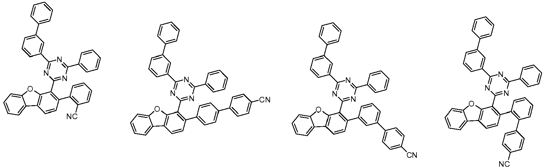


- The compound represented by the
Formula 1 can be prepared by sequentially performing the followingReaction Scheme 1,Reaction Scheme 2,Reaction Scheme 3, andReaction Scheme 4. The above preparation method can be further specified in the preparation example to be described later.


Reaction Schemes 1 to 4, - X1, X2, X3, X4, L1, L2, R1, R2, R3 and n are as defined above, and
- Y1, Y2, and Y3 are halogen.
- In addition, the present invention provides an organic light emitting device comprising the compound represented by
Formula 1. In one example, the present invention provides an organic light emitting device comprising a first electrode; a second electrode provided at a side opposite to the first electrode; and at least one layer of organic material layers provided between the first electrode and the second electrode, wherein the at least one layer of the organic material layers includes a compound represented byFormula 1. - The organic material layer of the organic light emitting device of the present invention may have a single layer structure, but it may have a multilayered structure in which two or more organic material layers are stacked. For example, the organic light emitting device of the present invention may have a structure comprising a hole injection layer, a hole transport layer, a light emitting layer, an electron transport layer, an electron injection layer and the like as the organic material layer. However, the structure of the organic light emitting device is not limited thereto, and it may include a smaller number of organic layers.
- Further, the organic material layer may include a hole injection layer, a hole transport layer, or a layer simultaneously performing hole injection and transport, wherein the hole injection layer, the hole transport layer, and the layer simultaneously performing hole injection and transport include a compound represented by
Formula 1. - Further, the organic material layer may include a light emitting layer, wherein the light emitting layer includes a compound represented by
Formula 1. - Further, the organic material layer may include an electron transport layer or an electron injection layer, wherein the electron transport layer or the electron injection layer include a compound represented by
Formula 1. - Further, the electron transport layer, the electron injection layer and the layer simultaneously performing an electron injection and an electron transport include a compound represented by
Formula 1. In particular, the compound represented by Formula I according to the present invention has excellent thermal stability and has a deep HOMO level of 6.0 eV or more, high triplet energy (ET), and hole stability. Further, when the compound represented byFormula 1 is used for an organic layer capable of performing electron injection and electron transport at the same time, an n-type dopant used in the art can be mixed and used. - Further, the organic material layer may include a light emitting layer or an electron transport layer, wherein the electron transport layer may include a compound represented by
Formula 1. - Further, the organic light emitting device according to the present invention may be a normal type organic light emitting device in which an anode, at least one organic material layer, and a cathode are sequentially stacked on a substrate. Further, the organic light emitting device according to the present invention may be an inverted type organic light emitting device in which a cathode, at least one organic material layer and an anode are sequentially stacked on a substrate. For example, the structure of an organic light emitting device according to an embodiment of the present invention is illustrated in
FIGS. 1 and 2 . -
FIG. 1 shows an example of an organic light emitting device comprising asubstrate 1, ananode 2, alight emitting layer 3, and acathode 4. In such a structure, the compound represented byFormula 1 may be included in the light emitting layer. -
FIG. 2 shows an example of an organic light emitting device comprising asubstrate 1, ananode 2, ahole injection layer 5, ahole transport layer 6, alight emitting layer 7, anelectron transport layer 8, and acathode 4. In such a structure, the compound represented byFormula 1 may be included in at least one layer of the hole injection layer, the hole transport layer, the light emitting layer and the electron transport layer. - The organic light emitting device according to the present invention may be manufactured by materials and methods known in the art, except that at least one layer of the organic material layers includes the compound represented by
Formula 1. In addition, when the organic light emitting device includes a plurality of organic material layers, the organic material layers may be formed of the same material or different materials. - For example, the organic light emitting device according to the present invention can be manufactured by sequentially stacking a first electrode, an organic material layer and a second electrode on a substrate. In this case, the organic light emitting device may be manufactured by depositing a metal, metal oxides having conductivity, or an alloy thereof on the substrate by using a PVD (physical vapor deposition) method such as a sputtering method or an e-beam evaporation method to form the anode, forming an organic material layer including the hole injection layer, the hole transport layer, the light emitting layer, and the electron transport layer thereon, and then depositing a material that can be used as the cathode thereon. In addition to such a method, the organic light emitting device may be manufactured by sequentially depositing a cathode material, an organic material layer and an anode material on a substrate.
- In addition, the compound represented by
Formula 1 may be formed into an organic layer by a solution coating method as well as a vacuum deposition method at the time of manufacturing an organic light emitting element. Herein, the solution coating method means a spin coating, a dip coating, a doctor blading, an inkjet printing, a screen printing, a spray method, a roll coating, or the like, but is not limited thereto. - In addition to such a method, the organic light emitting device may be manufactured by sequentially depositing a cathode material, an organic material layer, and an anode material on a substrate (International Publication
WO 2003/012890 ). However, the manufacturing method is not limited thereto. - For example, the first electrode is an anode and the second electrode is a cathode, or the first electrode is a cathode and the second electrode is an anode.
- As the anode material, generally, a material having a large work function is preferably used so that holes can be smoothly injected into the organic material layer. Specific examples of the anode material include metals such as vanadium, chrome, copper, zinc, and gold, or an alloy thereof; metal oxides such as zinc oxides, indium oxides, indium tin oxides (ITO), and indium zinc oxides (IZO); a combination of metals and oxides, such as ZnO:AI or SNO2:Sb; conductive polymers such as poly(3-methylthiophene), poly[3,4-(ethylene-1,2-dioxy)thiophene](PEDOT), polypyrrole, and polyaniline, and the like, but are not limited thereto.
- As the cathode material, generally, a material having a small work function is preferably used so that electrons can be easily injected into the organic material layer. Specific examples of the cathode material include metals such as magnesium, calcium, sodium, potassium, titanium, indium, yttrium, lithium, gadolinium, aluminum, silver, tin, and lead, or an alloy thereof; a multilayered structure material such as LiF/AI or LiO2/Al, and the like, but are not limited thereto.
- The hole injection layer is a layer for injecting holes from the electrode, and the hole injection material is preferably a compound which has an ability of transporting the holes, a hole injecting effect in the anode and an excellent hole injecting effect to the light emitting layer or the light emitting material, prevents movement of an exciton generated in the light emitting layer to the electron injection layer or the electron injection material, and has an excellent thin film forming ability. It is preferable that a HOMO (highest occupied molecular orbital) of the hole injection material is between the work function of the anode material and a HOMO of a peripheral organic material layer. Specific examples of the hole injection material include metal porphyrine, oligothiophene, an arylamine-based organic material, a hexanitrilehexaazatriphenylene-based organic material, a quinacridone-based organic material, a perylene-based organic material, anthraquinone, polyaniline and polythiophene-based conductive polymer, and the like, but are not limited thereto.
- The hole transport layer is a layer that receives holes from a hole injection layer and transports the holes to the light emitting layer. The hole transport material is suitably a material having large mobility to the holes, which may receive holes from the anode or the hole injection layer and transfer the holes to the light emitting layer. Specific examples thereof include an arylamine-based organic material, a conductive polymer, a block copolymer in which a conjugate portion and a non-conjugate portion are present together, and the like, but are not limited thereto.
- The light emitting material is a material capable of emitting light in the visible light region by combining holes and electrons respectively transported from the hole transport layer and the electron transport layer, and having good quantum efficiency for fluorescence or phosphorescence. Specific examples include 8-hydroxy-quinoline aluminum complex (Alq3); carbazole-based compounds; dimerized styryl compounds; BAlq; 10-hydroxybenzoquinoline-metal compounds; benzoxazole, benzothiazole and benzimidazole-based compunds; poly(p-phenylenevinylene)(PPV)-based polymers; spiro compounds; polyfluorene, rubrene, and the like, but are not limited thereto.
- The light emitting layer may include a host material and a dopant material. The host material may be a fused aromatic ring derivative, a heterocycle-containing compound or the like. Specific examples of the fused aromatic ring derivatives include anthracene derivatives, pyrene derivatives, naphthalene derivatives, pentacene derivatives, phenanthrene compounds, and fluoranthene compounds. Examples of heterocyclic compounds include carbazole derivatives, dibenzofuran derivatives, ladder-type furan compounds, pyrimidine derivatives, and the like, but are not limited thereto.
- Examples of the dopant material include an aromatic amine derivative, a styrylamine compound, a boron complex, a fluoranthene compound, a metal complex, and the like. Specific examples of the aromatic amine derivatives include substituted or unsubstituted fused aromatic ring derivatives having an arylamino group, examples thereof include pyrene, anthracene, chrysene, and periflanthene having the arylamino group, and the like, the styrylamine compound is a compound where at least one arylvinyl group is substituted in substituted or unsubstituted arylamine, in which one or two or more substituent groups selected from the group consisting of an aryl group, a silyl group, an alkyl group, a cycloalkyl group, and an arylamino group are substituted or unsubstituted. Specific examples thereof include styrylamine, styryldiamine, styryltriamine, styryltetramine, and the like, but are not limited thereto. Further, examples of the metal complex include an iridium complex, a platinum complex, and the like, but are not limited thereto.
- The electron transport layer is a layer receiving the electrons from the electron injection layer and transporting the electrons to the light emitting layer, the electron transport material is a material that can receive the electrons well from the cathode and transport the electrons to the light emitting layer, and a material having large mobility to the electrons is suitable. Specific examples thereof include an 8-hydroxyquinoline Al complex; a complex including Alq3; an organic radical compound; a hydroxyflavone-metal complex, and the like, but are not limited thereto. The electron transport layer may be used together with a predetermined desired cathode material as used according to the prior art. Particularly, an example of an appropriate cathode material is a general material having the low work function and followed by an aluminum layer or a silver layer. Specific examples thereof include cesium, barium, calcium, ytterbium, and samarium, and each case is followed by the aluminum layer or the silver layer.
- The electron injection layer is a layer injecting the electrons from the electrode, and a compound which has an ability of transporting the electrons, an electron injecting effect from the cathode, and an excellent electron injecting effect to the light emitting layer or the light emitting material, prevents movement of an exciton generated in the light emitting layer to the hole injection layer, and has an excellent thin film forming ability is preferable. Specific examples thereof include fluorenone, anthraquinodimethane, diphenoquinone, thiopyran dioxide, oxazole, oxadiazole, triazole, imidazole, perylene tetracarboxylic acid, fluorenylidene methane, anthrone, and the like, and its derivative, a metal complex compound, a nitrogen-containing 5-membered cycle derivative, and the like, but are not limited thereto.
- Examples of the metal complex compound include 8-hydroxyquinolinato lithium, bis(8-hydroxyquinolinato)zinc, bis(8-hydroxyquinolinato)copper, bis(8-hydroxyquinolinato)manganese, tris(8-hydroxyquinolinato)aluminum, tris(2-methyl-8-hydroxyquinolinato)aluminum, tris(8-hydroxyquinolinato)gallium, bis(10-hydroxybenzo[h]quinolinato)beryllium, bis(10-hydroxybenzo[h]quinolinato)zinc, bis(2-methyl-8-quinolinato)chlorogallium, bis(2-methyl-8-quinolinato)(o-cresolato)gallium, bis(2-methyl-8-quinolinato)(1-naphtholato)aluminum, bis(2-methyl-8-quinolinato)(2-naphtholato)gallium, and the like, but are not limited thereto.
- The organic light emitting device according to the present invention may be a front side emission type, a back side emission type, or a double side emission type according to the used material.
- In addition, the compound represented by
Formula 1 may be included in an organic solar cell or an organic transistor in addition to an organic light emitting device. - The preparation of the compound represented by
Formula 1 and the organic light emitting device comprising the same will be described in detail in the following examples. However, these examples are presented for illustrative purposes only, and the scope of the present invention is not limited thereto. -

- After a compound represented by Formula E1-P1-A (10.0 g, 38.0 mmol) and a compound represented by Formula E1-P1-B (10.0 g, 38.0 mmol) were completely dissolved in THF (100 mL), potassium carbonate (15.8 g, 114.0 mmol) was dissolved in 60 mL water and added thereto. Tetrakis triphenylphosphine palladium (1.3 g, 1.14 mmol) was added thereto, and then the mixture was heated and stirred for 8 hours. After the temperature was lowered to room temperature and the reaction was terminated, the potassium carbonate solution was removed and a white solid was filtered. The filtered white solid was washed twice with THF and ethyl acetate each time to prepare a compound represented by the Formula E1-P1 (13.5g, yield 89%).
MS[M+H]+=402
- After a compound represented by Formula E1-P1 (13.5 g, 33.6 mmol) was completely dissolved in acetonitrile (130 mL), potassium carbonate (13.9 g, 100.9 mmol) was dissolved in 55 mL water and added thereto. A compound represented by the Formula E1-P2-A (10.2 g, 33.6 mmol) was added dropwise to the reaction solution. After termination of the reaction, the potassium carbonate solution was removed and a white solid was filtered. The filtered white solid was washed twice with ethanol and water each time to prepare a compound represented by the Formula E1-P2 (20.9 g, yield 91%).
MS[M+H]+=684
- After a compound represented by the Formula E1-P2 (20.0 g, 29.3 mmol) and a compound represented by Formula E1-P3-A (7.5 g, 29.3 mmol) were completely dissolved in dioxane (200 mL), potassium acetate (8.6 g, 87.8 mmol) was added thereto, and then the mixture was heated and stirred. After the temperature was lowered to room temperature and the reaction was terminated, the potassium carbonate solution was removed and filtered to remove potassium carbonate. The white solid was washed twice with ethanol each time to prepare the compound represented by the Formula E1-P3 (12.7 g, yield 85%).
MS [M+H]+=512
- After a compound represented by Formula E1-P3 (12.0 g, 23.5 mmol) and a compound represented by Formula E1-A (6.3 g, 23.5 mmol) were completely dissolved in THF (120 mL), potassium carbonate (9.7 g, 70.4 mmol) was dissolved in 40 mL water and added thereto. Tetrakis triphenylphosphine palladium (0.8 g, 0.74 mmol) was added thereto, and then the mixture was heated and stirred for 8 hours. After the temperature was lowered to room temperature and the reaction was terminated, the potassium carbonate solution was removed and a white solid was filtered. The filtered white solid was washed twice with THF and ethyl acetate each time to prepare a compound represented by the Formula E1 (11.1 g, yield 77%).
MS[M+H]+=617 -

- The compound represented by the Formula E2-P1 was prepared in the same manner as in E1-P1 of Example 1, except that the respective starting materials were changed to those shown in the above Reaction Scheme.
MS [M+H]+=362
- The compound represented by the Formula E2-P2 was prepared in the same manner as in E2-P2 of Example 1, except that the respective starting materials were changed to those shown in the above Reaction Scheme.
MS [M+H]+=644
- The compound represented by the Formula E2-P3 was prepared in the same manner as in E1-P3 of Example 1, except that the respective starting materials were changed to those shown in the above Reaction Scheme.
MS [M+H]+=472
- The compound represented by the Formula E2 was prepared in the same manner as in E1 of Example 1, except that the respective starting materials were changed to those shown in the above Reaction Scheme.
MS [M+H]+=653 -

- The compound represented by the Formula E3-P1 was prepared in the same manner as in E1-P1 of Example 1, except that the respective starting materials were changed to those shown in the above Reaction Scheme.
MS [M+H]+=463
- The compound represented by the Formula E3-P2 was prepared in the same manner as in E1-P2 of Example 1, except that the respective starting materials were changed to those shown in the above Reaction Scheme.
MS [M+H]+=745
- The compound represented by the Formula E3-P3 was prepared in the same manner as in E1-P3 of Example 1, except that the respective starting materials were changed to those shown in the above Reaction Scheme.
MS [M+H]+=573
- The compound represented by the Formula E3 was prepared in the same manner as in E1 of Example 1, except that the respective starting materials were changed to those shown in the above Reaction Scheme.
MS [M+H]+=754 -

- The compound represented by the Formula E4 was prepared in the same manner as in E1 of Example 1, except that the respective starting materials were changed to those shown in the above Reaction Scheme.
MS [M+H]+=667 -

- The compound represented by the Formula E5 was prepared in the same manner as in E1 of Example 1, except that the respective starting materials were changed to those shown in the above Reaction Scheme.
MS [M+H]+=693 -

- The compound represented by the Formula E6 was prepared in the same manner as in E1 of Example 1, except that the respective starting materials were changed to those shown in the above Reaction Scheme.
MS [M+H]+=653 -

- The compound represented by the Formula E7 was prepared in the same manner as in E1 of Example 1, except that the respective starting materials were changed to those shown in the above Reaction Scheme.
MS [M+H]+=693 -

- The compound represented by the Formula E8 was prepared in the same manner as in E1 of Example 1, except that the respective starting materials were changed to those shown in the above Reaction Scheme.
MS [M+H]+=652 -

- The compound represented by the Formula E9 was prepared in the same manner as in E1 of Example 1, except that the respective starting materials were changed to those shown in the above Reaction Scheme.
MS [M+H]+=693 -

- The compound represented by the Formula E10 was prepared in the same manner as in E1 of Example 1, except that the respective starting materials were changed to those shown in the above Reaction Scheme.
MS [M+H]+=653 -

- The compound represented by the Formula E11 was prepared in the same manner as in E1 of Example 1, except that the respective starting materials were changed to those shown in the above Reaction Scheme.
MS [M+H]+=693 -

- The compound represented by the Formula E12 was prepared in the same manner as in E1 of Example 1, except that the respective starting materials were changed to those shown in the above Reaction Scheme.
MS [M+H]+=653 -

- The compound represented by the Formula E13 was prepared in the same manner as in E1 of Example 1, except that the respective starting materials were changed to those shown in the above Reaction Scheme.
MS [M+H]+=653 -

- The compound represented by the Formula E14 was prepared in the same manner as in E1 of Example 1, except that the respective starting materials were changed to those shown in the above Reaction Scheme.
MS [M+H]+=652 -

- The compound represented by the Formula E15 was prepared in the same manner as in E1 of Example 1, except that the respective starting materials were changed to those shown in the above Reaction Scheme.
MS [M+H]+=577 -

- The compound represented by the Formula E16 was prepared in the same manner as in E1 of Example 1, except that the respective starting materials were changed to those shown in the above Reaction Scheme.
MS [M+H]+=693 -

- The compound represented by the Formula E17 was prepared in the same manner as in E1 of Example 1, except that the respective starting materials were changed to those shown in the above Reaction Scheme.
MS [M+H]+=577 -

- The compound represented by the Formula E18 was prepared in the same manner as in E1 of Example 1, except that the respective starting materials were changed to those shown in the above Reaction Scheme.
MS [M+H]+=567 -

- The compound represented by the Formula E19 was prepared in the same manner as in E1 of Example 1, except that the respective starting materials were changed to those shown in the above Reaction Scheme.
MS [M+H]+=593 -

- The compound represented by the Formula E20 was prepared in the same manner as in E1 of Example 1, except that the respective starting materials were changed to those shown in the above Reaction Scheme.
MS [M+H]+=745 -

- The compound represented by the Formula E21 was prepared in the same manner as in E1 of Example 1, except that the respective starting materials were changed to those shown in the above Reaction Scheme.
MS [M+H]+=669 -

- The compound represented by the Formula E22 was prepared in the same manner as in E1 of Example 1, except that the respective starting materials were changed to those shown in the above Reaction Scheme.
MS [M+H]+=709 - A glass substrate on which a thin film of ITO (indium tin oxide) was coated in a thickness of 1,000 Å was put into distilled water containing the detergent dissolved therein and washed by the ultrasonic wave. The used detergent was a product commercially available from Fisher Co. and the distilled water was one which had been twice filtered by using a filter commercially available from Millipore Co. The ITO was washed for 30 minutes, and ultrasonic washing was then repeated twice for 10 minutes by using distilled water. After the washing with distilled water was completed, the substrate was ultrasonically washed with isopropyl alcohol, acetone, and methanol solvent, and dried, after which it was transported to a plasma cleaner. Then, the substrate was cleaned with oxygen plasma for 5 minutes, and then transferred to a vacuum evaporator.
- On the ITO transparent electrode thus prepared, a compound HI-A below was thermally vacuum-deposited in a thickness of 600 Å to form a hole injection layer. A compound HAT (50 Å) below and a compound HT-A (600 Å) below were sequentially vacuum-deposited on the hole injection layer to form a hole transport.
- Then, a compound BH below and a compound BD below were vacuum-deposited at a weight ratio of 25: 1 on the electron transport layer in a film thickness of 20 nm to form a light emitting layer.
- The compound E1 of Example 1 and a compound LIQ below were vacuum-deposited at a weight ratio of 1: 1 on the light emitting layer in a thickness of 350 Å to form an electron injection and transport layer. A lithium fluoride (LiF) in a thickness of 10 Å and aluminum in a thickness of 1,000 Å were sequentially deposited on the electron injection and transport layer to form a cathode.
- In the above process, the vapor deposition rate of the organic material was maintained at 0.4 to 0.9 Å/sec, the vapor deposition rate of lithium fluoride of the cathode was maintained at 0.3 Å/sec, the vapor deposition rate of aluminum was maintained at 2 Å/sec, and the degree of vacuum during vapor deposition was maintained at 1×10⁻⁷∼5×10⁻⁵ torr to manufacture an organic light emitting device.


- The organic light emitting devices were manufactured in the same manner as in Experimental Example 1, except that the compounds E2 to E22 of Examples 2 to 22 were used instead of the compound E1 of Example 1.


- The organic light emitting devices were manufactured in the same manner as in Experimental Example 1, except that the above compounds ET-A to ET-K were used instead of the compound E1 of Example 1.
- The driving voltage and light emitting efficiency were measured at the current density of 10 mA/cm2 for the organic light emitting devices manufactured in the Examples and Comparative Examples, and the time (T90) at which the luminance became 90% relative to the initial luminance at the current density of 20 mA/cm2 was measured. The above results are shown in Tables 1 and 2.
[Table 1] Class Voltage (V@10 mA/cm2) Efficiency (cd/A@10 mA/cm2) Color coordinate (x, y) Lifetime(h) T90 at 20 mA/cm2) Experimental Example 1(E1) 4.47 5.01 (0.142, 0.096) 270 Experimental Example 2(E2) 4.50 4.95 (0.142, 0.096) 300 Experimental Example 3(E3) 4.66 4.80 (0.142, 0.096) 410 Experimental Example 4(E4) 4.51 4.94 (0.142, 0.096) 314 Experimental Example 5(E5) 4.45 5.05 (0.142, 0.096) 266 Experimental Example 6(E6) 4.40 5.10 (0.142, 0.097) 245 Experimental Example 7(E7) 4.39 5.08 (0.142, 0.096) 239 Experimental Example 8(E8) 4.39 5.11 (0.142, 0.099) 230 Experimental Example 9(E9) 4.41 5.09 (0.142, 0.096) 255 Experimental Example 10(E10) 4.43 5.06 (0.142, 0.099) 261 Experimental Example 11 (E11) 4.42 5.13 (0.142, 0.096) 244 Experimental Example 12(E12) 4.33 5.08 (0.142, 0.097) 240 Experimental Example 13(E13) 4.48 5.03 (0.142, 0.096) 284 Experimental Example 14(E14) 4.37 5.11 (0.142, 0.096) 266 Experimental Example 15(E15) 4.47 4.99 (0.142, 0.096) 299 Experimental Example 16(E16) 4.40 5.15 (0.142, 0.097) 235 Experimental Example 17(E17) 4.33 5.20 (0.142, 0.096) 233 Experimental Example 18(E18) 4.47 5.00 (0.142, 0.096) 301 Experimental Example 19(E19) 4.32 5.18 (0.142, 0.096) 231 Experimental Example 20(E20) 4.41 5.07 (0.142, 0.095) 287 Experimental Example 21(E21) 4.40 5.08 (0.142, 255 Experimental Example 22(E22) 4.41 5.12 (0.142, 0.096) 260 [Table 2] Class Voltage (V@10 mA/cm2) Efficiency (cd/A@10 mA/cm2) Color coordinate (x, y) Lifetime(h) T90 at 20 mA/cm2) Comparative Example 1(ET-A) 6.00 3.14 (0.142, 0.096) 170 Comparative Example 2(ET-B) 5.12 3.77 (0.142, 0.096) 142 Comparative Example 3(ET-C) 5.01 3.83 (0.142, 0.096) 88 Comparative Example 4(ET-D) 5.16 3.83 (0.142, 0.096) 55 Comparative Example 5(ET-E) 5.07 3.80 (0.142, 0.096) 74 Comparative Example 6(ET-F) 5.05 3.81 (0.142, 0.096) 73 Comparative Example 7(ET-G) 5.11 3.76 (0.142, 0.097) 80 Comparative Example 8(ET-H) 5.89 3.04 (0.142, 180 Comparative Example 9(ET-I) 5.12 3.69 (0.142, 0.096) 91 Comparative Example 10(ET-J) 6.10 3.04 (0.142, 0.099) 20 Comparative Example 11(ET-K) 6.18 3.90 (0.142, 0.096) 19 - As shown in Table 1, it was confirmed that the compound represented by
Formula 1 according to the present invention can be used for an organic material layer capable of simultaneously performing electron injection and electron transport of the organic light-emitting device. - In addition, when comparing the Experimental Examples in Table 1 and the Comparative Experimental Examples 2, 3, 4, 8 and 9 in Table 2, it was confirmed that the compounds of
Formula 1 according to the present invention were remarkably excellent in terms of driving voltage, efficiency, and lifetime of the organic light emitting device as compared with a compound in which a triazine (or pyrimidine) and a heteroaryl group different from theFormula 1 were substituted in dibenzofuran (or dibenzothiophene). - Further, when comparing the Experimental Examples in Table 1 and the Comparative Experimental Example 1 in Table 2, it was confirmed that the compounds of
Formula 1 according to the present invention were remarkably excellent in terms of driving voltage, efficiency, and lifetime of the organic light emitting device as compared with a compound in which a cyano group and a heteroaryl group different from theFormula 1 were substituted in dibenzofuran (or dibenzothiophene). - Further, when comparing the Experimental Examples in Table 1 and the Comparative Experimental Examples 5, 6 and 7 in Table 2, it was confirmed that the compounds of
Formula 1 according to the present invention were remarkably excellent in terms of driving voltage, efficiency, and lifetime of the organic light emitting device as compared with a compound in which only a triazine (or pyrimidine) was substituted in dibenzofuran (or dibenzothiophene). - Further, when comparing the Experimental Examples in Table 1 and the Comparative Experimental Example 10 in Table 2, it was confirmed that the compounds of
Formula 1 according to the present invention were remarkably excellent in terms of driving voltage, efficiency, and lifetime of the organic light emitting device as compared with a compound in which only a heteroaryl group other than cyano group was substituted in dibenzofuran (or dibenzothiophene). - Further, when comparing the Experimental Examples in Table 1 and the Comparative Experimental Example 11 in Table 2, it was confirmed that the compounds of
Formula 1 according to the present invention were remarkably excellent in terms of driving voltage, efficiency, and lifetime of the organic light emitting device as compared in which triazine (or pyrimidine) and a cyano group each are substituted in different phenyl groups of dibenzofuran (or dibenzothiophene).[Explanation of Sign] 1: substrate, 2: anode, 3: light emitting layer 4: cathode 5: hole injection layer 6: hole transport layer 7: light emitting layer 8: electron transport layer
Claims (10)
- A compound represented by Formula 1 below:
 X1 is O or S,X2, X3 and X4 are each independently N or CH,L1 and L2 are each independently a single bond; or a substituted or unsubstituted C6-60 arylene; or a substituted or unsubstituted C2-60 heteroarylene containing at least one of N, O and S,R1 and R2 are each independently a substituted or unsubstituted C6-60 aryl; or a substituted or unsubstituted C2-60 heteroaryl containing at least one of N, O and S,R3 is each independently a C6-60 aryl substituted with one or two cyano, andn is an integer of 1 or 2.
 - The compound of claim 1, wherein at least two of X2, X3 and X4 are N.
- The compound of claim 1, wherein
L1 and L2 are each independently a single bond, or any one selected from the group consisting of the following:


- The compound of claim 1, wherein
L1 and L2 are each independently a single bond,
- The compound of claim 1, wherein
R1 and R2 are each independently any one selected from the group consisting of the following:


- The compound of claim 1, wherein
R1 and R2 are each independently

- The compound of claim 1, wherein
each R3 is independently any one selected from the group consisting of phenyl substituted with one or two cyano, biphenylyl substituted with one or two cyano, terphenylyl substituted with one or two cyano, or dimethylfluorenyl substituted with one or two cyano. - The compound of claim 1, wherein
the compound represented by Formula 1 is any one selected from the group consisting of the following:


- An organic light emitting device comprising a first electrode; a second electrode provided at a side opposite to the first electrode; and at least one layer of the organic material layers provided between the first electrode and the second electrode, wherein the at least one layer of the organic material layers includes a compound according to any one of claims 1 to 8.
- The organic light emitting device of claim, 9, wherein the organic material layer comprising the compound is an electron injection layer; an electron transport layer; or a layer simultaneously performing electron injection and electron transport.
Applications Claiming Priority (3)
| Application Number | Priority Date | Filing Date | Title |
|---|---|---|---|
| KR20170009884 | 2017-01-20 | ||
| KR1020180001717A KR102003351B1 (en) | 2017-01-20 | 2018-01-05 | Novel hetero-cyclic compound and organic light emitting device comprising the same |
| PCT/KR2018/000486 WO2018135798A1 (en) | 2017-01-20 | 2018-01-10 | Novel heterocyclic compound and organic light emitting element using same |
Publications (3)
| Publication Number | Publication Date |
|---|---|
| EP3527564A1 true EP3527564A1 (en) | 2019-08-21 |
| EP3527564A4 EP3527564A4 (en) | 2019-11-20 |
| EP3527564B1 EP3527564B1 (en) | 2022-03-02 |
Family
ID=63048391
Family Applications (1)
| Application Number | Title | Priority Date | Filing Date |
|---|---|---|---|
| EP18741013.9A Active EP3527564B1 (en) | 2017-01-20 | 2018-01-10 | Novel heterocyclic compound and organic light emitting element using same |
Country Status (6)
| Country | Link |
|---|---|
| US (1) | US11228001B2 (en) |
| EP (1) | EP3527564B1 (en) |
| JP (1) | JP6801162B2 (en) |
| KR (1) | KR102003351B1 (en) |
| CN (1) | CN110023306B (en) |
| TW (1) | TWI695833B (en) |
Families Citing this family (6)
| Publication number | Priority date | Publication date | Assignee | Title |
|---|---|---|---|---|
| KR102017790B1 (en) | 2017-04-13 | 2019-09-03 | 주식회사 엘지화학 | Novel hetero-cyclic compound and organic light emitting device comprising the same |
| KR102536248B1 (en) | 2017-06-21 | 2023-05-25 | 삼성디스플레이 주식회사 | Heterocyclic compound and organic light emitting device comprising the same |
| KR102415376B1 (en) | 2017-08-04 | 2022-07-01 | 삼성디스플레이 주식회사 | Condensed-cyclic compound and organic light emitting device comprising the same |
| KR102536246B1 (en) * | 2018-03-23 | 2023-05-25 | 삼성디스플레이 주식회사 | Heterocyclic compound and organic light emitting device comprising the same |
| KR102341241B1 (en) * | 2018-11-23 | 2021-12-20 | 주식회사 엘지화학 | Novel compound and organic light emitting device comprising the same |
| CN111018847A (en) * | 2019-10-31 | 2020-04-17 | 陕西莱特光电材料股份有限公司 | Nitrogen-containing compound, electronic component, and electronic device |
Family Cites Families (23)
| Publication number | Priority date | Publication date | Assignee | Title |
|---|---|---|---|---|
| KR100430549B1 (en) | 1999-01-27 | 2004-05-10 | 주식회사 엘지화학 | New organomattalic complex molecule for the fabrication of organic light emitting diodes |
| DE10135513B4 (en) | 2001-07-20 | 2005-02-24 | Novaled Gmbh | Light-emitting component with organic layers |
| US9484539B2 (en) * | 2012-07-19 | 2016-11-01 | Lg Chem, Ltd. | Polycyclic compound and organic electronic device comprising the same |
| WO2014017844A1 (en) | 2012-07-26 | 2014-01-30 | 주식회사 동진쎄미켐 | Organic light-emitting compound comprising acridine derivatives, and organic light-emitting device comprising same |
| KR101672074B1 (en) | 2013-05-07 | 2016-11-02 | 주식회사 엘지화학 | Hetero-cyclic compound and organic electronic device comprising the same |
| KR102167042B1 (en) * | 2013-09-06 | 2020-10-19 | 삼성디스플레이 주식회사 | Condensed compound and organic light emitting diode comprising the same |
| KR102191991B1 (en) * | 2013-09-06 | 2020-12-17 | 삼성디스플레이 주식회사 | Condensed compound and organic light emitting diode comprising the same |
| KR102145888B1 (en) | 2013-12-13 | 2020-08-20 | 삼성디스플레이 주식회사 | Triazine-based compounds and organic light-emitting devices comprising the same |
| TW201542500A (en) * | 2013-12-26 | 2015-11-16 | 羅門哈斯電子材料韓國公司 | An organic electroluminescent compound and an organic electroluminescent device comprising the same |
| JP6890975B2 (en) | 2014-05-05 | 2021-06-18 | メルク パテント ゲーエムベーハー | Materials for OLED devices |
| US9732069B2 (en) | 2014-05-21 | 2017-08-15 | Samsung Electronics Co., Ltd. | Carbazole compound and organic light emitting device including the same |
| US10297762B2 (en) | 2014-07-09 | 2019-05-21 | Universal Display Corporation | Organic electroluminescent materials and devices |
| US10644247B2 (en) * | 2015-02-06 | 2020-05-05 | Universal Display Corporation | Organic electroluminescent materials and devices |
| JP5831654B1 (en) | 2015-02-13 | 2015-12-09 | コニカミノルタ株式会社 | Aromatic heterocycle derivative, organic electroluminescence device using the same, illumination device and display device |
| KR102342339B1 (en) * | 2015-03-18 | 2021-12-22 | 에스에프씨주식회사 | Novel organic compounds for organic light-emitting diode and organic light-emitting diode including the same |
| EP3072943B1 (en) | 2015-03-26 | 2018-05-02 | Idemitsu Kosan Co., Ltd. | Dibenzofuran/carbazole-substituted benzonitriles |
| KR102486381B1 (en) * | 2015-08-13 | 2023-01-09 | 삼성전자주식회사 | Condensed cyclic compound and organic light emitting device including the same |
| KR102541267B1 (en) * | 2015-10-05 | 2023-06-12 | 삼성전자주식회사 | Condensed cyclic compound and organic light emitting device including the same |
| US11329230B2 (en) * | 2016-04-29 | 2022-05-10 | Samsung Display Co., Ltd. | Organic light-emitting device |
| KR20180001290A (en) * | 2016-06-27 | 2018-01-04 | 삼성전자주식회사 | Condensed cyclic compound, mixture including the same and organic light emitting device including the same |
| KR101849747B1 (en) * | 2016-07-20 | 2018-05-31 | 주식회사 엘지화학 | Novel hetero-cyclic compound and organic light emitting device comprising the same |
| KR20190079341A (en) * | 2017-12-27 | 2019-07-05 | 삼성에스디아이 주식회사 | Organic compound and composition and organic optoelectronic device and display device |
| KR102536246B1 (en) * | 2018-03-23 | 2023-05-25 | 삼성디스플레이 주식회사 | Heterocyclic compound and organic light emitting device comprising the same |
-
2018
- 2018-01-05 KR KR1020180001717A patent/KR102003351B1/en active IP Right Grant
- 2018-01-10 JP JP2019521771A patent/JP6801162B2/en active Active
- 2018-01-10 US US16/341,884 patent/US11228001B2/en active Active
- 2018-01-10 CN CN201880004727.3A patent/CN110023306B/en active Active
- 2018-01-10 EP EP18741013.9A patent/EP3527564B1/en active Active
- 2018-01-15 TW TW107101370A patent/TWI695833B/en active
Also Published As
| Publication number | Publication date |
|---|---|
| KR20180086126A (en) | 2018-07-30 |
| US11228001B2 (en) | 2022-01-18 |
| KR102003351B1 (en) | 2019-07-23 |
| JP6801162B2 (en) | 2020-12-16 |
| EP3527564B1 (en) | 2022-03-02 |
| JP2019535679A (en) | 2019-12-12 |
| EP3527564A4 (en) | 2019-11-20 |
| US20190245149A1 (en) | 2019-08-08 |
| CN110023306A (en) | 2019-07-16 |
| CN110023306B (en) | 2022-09-27 |
| TW201831470A (en) | 2018-09-01 |
| TWI695833B (en) | 2020-06-11 |
Similar Documents
| Publication | Publication Date | Title |
|---|---|---|
| EP3373353B1 (en) | Organic light-emitting element | |
| EP3567032B1 (en) | Heterocyclic compound and organic light-emitting element utilizing same | |
| EP3392242B1 (en) | Novel heterocyclic compound and organic light-emitting device using same | |
| KR102095001B1 (en) | Novel hetero-cyclic compound and organic light emitting device comprising the same | |
| EP3477720B1 (en) | Organic light emitting element | |
| EP3567026B1 (en) | Novel compound and organic light-emitting device using same | |
| EP3539953B1 (en) | Novel compound and organic light-emitting device using same | |
| EP3527564A1 (en) | Novel heterocyclic compound and organic light emitting element using same | |
| EP3556750B1 (en) | Novel compound and organic light-emitting element including same | |
| EP3546453B1 (en) | Novel heterocyclic compound and organic light emitting element using same | |
| EP3862350A1 (en) | Novel compound and organic light emitting device using same | |
| EP3369718B1 (en) | Spiro-type compound and organic light emitting element comprising same | |
| KR102576227B1 (en) | Novel compound and organic light emitting device comprising the same | |
| CN112424191A (en) | Novel compound and organic light emitting device comprising the same | |
| EP3372593B1 (en) | Novel compound and organic light emitting element comprising same | |
| EP3747873B1 (en) | Novel compound and organic light emitting diode using same | |
| US20210053934A1 (en) | Compound and organic light emitting device comprising the same | |
| KR102474920B1 (en) | Novel compound and organic light emitting device comprising the same | |
| KR20220040762A (en) | Novel compound and organic light emitting device comprising the same | |
| EP4335845A1 (en) | Novel compound and organic light emitting device comprising the same | |
| EP4242205A1 (en) | Novel compound and organic light emitting device comprising same | |
| KR102663117B1 (en) | Novel compound and organic light emitting device comprising the same | |
| KR102592035B1 (en) | Novel compound and organic light emitting device comprising the same | |
| EP4299574A1 (en) | Novel compound and organic light-emitting device comprising same | |
| KR102521449B1 (en) | Novel hetero-cyclic compound and organic light emitting device comprising the same |
Legal Events
| Date | Code | Title | Description |
|---|---|---|---|
| STAA | Information on the status of an ep patent application or granted ep patent |
Free format text: STATUS: THE INTERNATIONAL PUBLICATION HAS BEEN MADE |
|
| PUAI | Public reference made under article 153(3) epc to a published international application that has entered the european phase |
Free format text: ORIGINAL CODE: 0009012 |
|
| STAA | Information on the status of an ep patent application or granted ep patent |
Free format text: STATUS: REQUEST FOR EXAMINATION WAS MADE |
|
| 17P | Request for examination filed |
Effective date: 20190516 |
|
| AK | Designated contracting states |
Kind code of ref document: A1 Designated state(s): AL AT BE BG CH CY CZ DE DK EE ES FI FR GB GR HR HU IE IS IT LI LT LU LV MC MK MT NL NO PL PT RO RS SE SI SK SM TR |
|
| AX | Request for extension of the european patent |
Extension state: BA ME |
|
| A4 | Supplementary search report drawn up and despatched |
Effective date: 20191017 |
|
| RIC1 | Information provided on ipc code assigned before grant |
Ipc: C07D 409/14 20060101ALI20191011BHEP Ipc: C07D 307/91 20060101ALI20191011BHEP Ipc: C07D 405/04 20060101AFI20191011BHEP Ipc: C07D 333/76 20060101ALI20191011BHEP Ipc: H01L 51/50 20060101ALI20191011BHEP Ipc: C07D 251/24 20060101ALI20191011BHEP Ipc: H01L 51/00 20060101ALI20191011BHEP |
|
| DAV | Request for validation of the european patent (deleted) | ||
| DAX | Request for extension of the european patent (deleted) | ||
| STAA | Information on the status of an ep patent application or granted ep patent |
Free format text: STATUS: EXAMINATION IS IN PROGRESS |
|
| 17Q | First examination report despatched |
Effective date: 20210331 |
|
| GRAP | Despatch of communication of intention to grant a patent |
Free format text: ORIGINAL CODE: EPIDOSNIGR1 |
|
| STAA | Information on the status of an ep patent application or granted ep patent |
Free format text: STATUS: GRANT OF PATENT IS INTENDED |
|
| INTG | Intention to grant announced |
Effective date: 20211119 |
|
| GRAS | Grant fee paid |
Free format text: ORIGINAL CODE: EPIDOSNIGR3 |
|
| GRAA | (expected) grant |
Free format text: ORIGINAL CODE: 0009210 |
|
| STAA | Information on the status of an ep patent application or granted ep patent |
Free format text: STATUS: THE PATENT HAS BEEN GRANTED |
|
| AK | Designated contracting states |
Kind code of ref document: B1 Designated state(s): AL AT BE BG CH CY CZ DE DK EE ES FI FR GB GR HR HU IE IS IT LI LT LU LV MC MK MT NL NO PL PT RO RS SE SI SK SM TR |
|
| REG | Reference to a national code |
Ref country code: GB Ref legal event code: FG4D |
|
| REG | Reference to a national code |
Ref country code: CH Ref legal event code: EP Ref country code: AT Ref legal event code: REF Ref document number: 1472165 Country of ref document: AT Kind code of ref document: T Effective date: 20220315 |
|
| REG | Reference to a national code |
Ref country code: DE Ref legal event code: R096 Ref document number: 602018031624 Country of ref document: DE |
|
| REG | Reference to a national code |
Ref country code: IE Ref legal event code: FG4D |
|
| REG | Reference to a national code |
Ref country code: LT Ref legal event code: MG9D |
|
| REG | Reference to a national code |
Ref country code: NL Ref legal event code: MP Effective date: 20220302 |
|
| PG25 | Lapsed in a contracting state [announced via postgrant information from national office to epo] |
Ref country code: SE Free format text: LAPSE BECAUSE OF FAILURE TO SUBMIT A TRANSLATION OF THE DESCRIPTION OR TO PAY THE FEE WITHIN THE PRESCRIBED TIME-LIMIT Effective date: 20220302 Ref country code: RS Free format text: LAPSE BECAUSE OF FAILURE TO SUBMIT A TRANSLATION OF THE DESCRIPTION OR TO PAY THE FEE WITHIN THE PRESCRIBED TIME-LIMIT Effective date: 20220302 Ref country code: NO Free format text: LAPSE BECAUSE OF FAILURE TO SUBMIT A TRANSLATION OF THE DESCRIPTION OR TO PAY THE FEE WITHIN THE PRESCRIBED TIME-LIMIT Effective date: 20220602 Ref country code: LT Free format text: LAPSE BECAUSE OF FAILURE TO SUBMIT A TRANSLATION OF THE DESCRIPTION OR TO PAY THE FEE WITHIN THE PRESCRIBED TIME-LIMIT Effective date: 20220302 Ref country code: HR Free format text: LAPSE BECAUSE OF FAILURE TO SUBMIT A TRANSLATION OF THE DESCRIPTION OR TO PAY THE FEE WITHIN THE PRESCRIBED TIME-LIMIT Effective date: 20220302 Ref country code: ES Free format text: LAPSE BECAUSE OF FAILURE TO SUBMIT A TRANSLATION OF THE DESCRIPTION OR TO PAY THE FEE WITHIN THE PRESCRIBED TIME-LIMIT Effective date: 20220302 Ref country code: BG Free format text: LAPSE BECAUSE OF FAILURE TO SUBMIT A TRANSLATION OF THE DESCRIPTION OR TO PAY THE FEE WITHIN THE PRESCRIBED TIME-LIMIT Effective date: 20220602 |
|
| REG | Reference to a national code |
Ref country code: AT Ref legal event code: MK05 Ref document number: 1472165 Country of ref document: AT Kind code of ref document: T Effective date: 20220302 |
|
| PG25 | Lapsed in a contracting state [announced via postgrant information from national office to epo] |
Ref country code: PL Free format text: LAPSE BECAUSE OF FAILURE TO SUBMIT A TRANSLATION OF THE DESCRIPTION OR TO PAY THE FEE WITHIN THE PRESCRIBED TIME-LIMIT Effective date: 20220302 Ref country code: LV Free format text: LAPSE BECAUSE OF FAILURE TO SUBMIT A TRANSLATION OF THE DESCRIPTION OR TO PAY THE FEE WITHIN THE PRESCRIBED TIME-LIMIT Effective date: 20220302 Ref country code: GR Free format text: LAPSE BECAUSE OF FAILURE TO SUBMIT A TRANSLATION OF THE DESCRIPTION OR TO PAY THE FEE WITHIN THE PRESCRIBED TIME-LIMIT Effective date: 20220603 Ref country code: FI Free format text: LAPSE BECAUSE OF FAILURE TO SUBMIT A TRANSLATION OF THE DESCRIPTION OR TO PAY THE FEE WITHIN THE PRESCRIBED TIME-LIMIT Effective date: 20220302 |
|
| PG25 | Lapsed in a contracting state [announced via postgrant information from national office to epo] |
Ref country code: NL Free format text: LAPSE BECAUSE OF FAILURE TO SUBMIT A TRANSLATION OF THE DESCRIPTION OR TO PAY THE FEE WITHIN THE PRESCRIBED TIME-LIMIT Effective date: 20220302 |
|
| PG25 | Lapsed in a contracting state [announced via postgrant information from national office to epo] |
Ref country code: SM Free format text: LAPSE BECAUSE OF FAILURE TO SUBMIT A TRANSLATION OF THE DESCRIPTION OR TO PAY THE FEE WITHIN THE PRESCRIBED TIME-LIMIT Effective date: 20220302 Ref country code: SK Free format text: LAPSE BECAUSE OF FAILURE TO SUBMIT A TRANSLATION OF THE DESCRIPTION OR TO PAY THE FEE WITHIN THE PRESCRIBED TIME-LIMIT Effective date: 20220302 Ref country code: RO Free format text: LAPSE BECAUSE OF FAILURE TO SUBMIT A TRANSLATION OF THE DESCRIPTION OR TO PAY THE FEE WITHIN THE PRESCRIBED TIME-LIMIT Effective date: 20220302 Ref country code: PT Free format text: LAPSE BECAUSE OF FAILURE TO SUBMIT A TRANSLATION OF THE DESCRIPTION OR TO PAY THE FEE WITHIN THE PRESCRIBED TIME-LIMIT Effective date: 20220704 Ref country code: EE Free format text: LAPSE BECAUSE OF FAILURE TO SUBMIT A TRANSLATION OF THE DESCRIPTION OR TO PAY THE FEE WITHIN THE PRESCRIBED TIME-LIMIT Effective date: 20220302 Ref country code: CZ Free format text: LAPSE BECAUSE OF FAILURE TO SUBMIT A TRANSLATION OF THE DESCRIPTION OR TO PAY THE FEE WITHIN THE PRESCRIBED TIME-LIMIT Effective date: 20220302 Ref country code: AT Free format text: LAPSE BECAUSE OF FAILURE TO SUBMIT A TRANSLATION OF THE DESCRIPTION OR TO PAY THE FEE WITHIN THE PRESCRIBED TIME-LIMIT Effective date: 20220302 |
|
| PG25 | Lapsed in a contracting state [announced via postgrant information from national office to epo] |
Ref country code: IS Free format text: LAPSE BECAUSE OF FAILURE TO SUBMIT A TRANSLATION OF THE DESCRIPTION OR TO PAY THE FEE WITHIN THE PRESCRIBED TIME-LIMIT Effective date: 20220702 Ref country code: AL Free format text: LAPSE BECAUSE OF FAILURE TO SUBMIT A TRANSLATION OF THE DESCRIPTION OR TO PAY THE FEE WITHIN THE PRESCRIBED TIME-LIMIT Effective date: 20220302 |
|
| REG | Reference to a national code |
Ref country code: DE Ref legal event code: R097 Ref document number: 602018031624 Country of ref document: DE |
|
| PLBE | No opposition filed within time limit |
Free format text: ORIGINAL CODE: 0009261 |
|
| STAA | Information on the status of an ep patent application or granted ep patent |
Free format text: STATUS: NO OPPOSITION FILED WITHIN TIME LIMIT |
|
| PG25 | Lapsed in a contracting state [announced via postgrant information from national office to epo] |
Ref country code: DK Free format text: LAPSE BECAUSE OF FAILURE TO SUBMIT A TRANSLATION OF THE DESCRIPTION OR TO PAY THE FEE WITHIN THE PRESCRIBED TIME-LIMIT Effective date: 20220302 |
|
| 26N | No opposition filed |
Effective date: 20221205 |
|
| PG25 | Lapsed in a contracting state [announced via postgrant information from national office to epo] |
Ref country code: SI Free format text: LAPSE BECAUSE OF FAILURE TO SUBMIT A TRANSLATION OF THE DESCRIPTION OR TO PAY THE FEE WITHIN THE PRESCRIBED TIME-LIMIT Effective date: 20220302 |
|
| PGFP | Annual fee paid to national office [announced via postgrant information from national office to epo] |
Ref country code: DE Payment date: 20221220 Year of fee payment: 6 |
|
| PG25 | Lapsed in a contracting state [announced via postgrant information from national office to epo] |
Ref country code: IT Free format text: LAPSE BECAUSE OF FAILURE TO SUBMIT A TRANSLATION OF THE DESCRIPTION OR TO PAY THE FEE WITHIN THE PRESCRIBED TIME-LIMIT Effective date: 20220302 |
|
| REG | Reference to a national code |
Ref country code: CH Ref legal event code: PL |
|
| PG25 | Lapsed in a contracting state [announced via postgrant information from national office to epo] |
Ref country code: LU Free format text: LAPSE BECAUSE OF NON-PAYMENT OF DUE FEES Effective date: 20230110 |
|
| REG | Reference to a national code |
Ref country code: BE Ref legal event code: MM Effective date: 20230131 |
|
| PG25 | Lapsed in a contracting state [announced via postgrant information from national office to epo] |
Ref country code: LI Free format text: LAPSE BECAUSE OF NON-PAYMENT OF DUE FEES Effective date: 20230131 Ref country code: CH Free format text: LAPSE BECAUSE OF NON-PAYMENT OF DUE FEES Effective date: 20230131 |
|
| PG25 | Lapsed in a contracting state [announced via postgrant information from national office to epo] |
Ref country code: BE Free format text: LAPSE BECAUSE OF NON-PAYMENT OF DUE FEES Effective date: 20230131 |
|
| PGFP | Annual fee paid to national office [announced via postgrant information from national office to epo] |
Ref country code: GB Payment date: 20231220 Year of fee payment: 7 |
|
| PG25 | Lapsed in a contracting state [announced via postgrant information from national office to epo] |
Ref country code: IE Free format text: LAPSE BECAUSE OF NON-PAYMENT OF DUE FEES Effective date: 20230110 |
|
| PGFP | Annual fee paid to national office [announced via postgrant information from national office to epo] |
Ref country code: FR Payment date: 20231222 Year of fee payment: 7 |