EP3525344A1 - An electronic converter, related audio system, integrated circuit and method of operating an electronic converter - Google Patents
An electronic converter, related audio system, integrated circuit and method of operating an electronic converter Download PDFInfo
- Publication number
- EP3525344A1 EP3525344A1 EP19154017.8A EP19154017A EP3525344A1 EP 3525344 A1 EP3525344 A1 EP 3525344A1 EP 19154017 A EP19154017 A EP 19154017A EP 3525344 A1 EP3525344 A1 EP 3525344A1
- Authority
- EP
- European Patent Office
- Prior art keywords
- voltage
- output terminal
- terminal
- inductor
- charge
- Prior art date
- Legal status (The legal status is an assumption and is not a legal conclusion. Google has not performed a legal analysis and makes no representation as to the accuracy of the status listed.)
- Granted
Links
Images






Classifications
-
- H—ELECTRICITY
- H02—GENERATION; CONVERSION OR DISTRIBUTION OF ELECTRIC POWER
- H02M—APPARATUS FOR CONVERSION BETWEEN AC AND AC, BETWEEN AC AND DC, OR BETWEEN DC AND DC, AND FOR USE WITH MAINS OR SIMILAR POWER SUPPLY SYSTEMS; CONVERSION OF DC OR AC INPUT POWER INTO SURGE OUTPUT POWER; CONTROL OR REGULATION THEREOF
- H02M3/00—Conversion of DC power input into DC power output
- H02M3/02—Conversion of DC power input into DC power output without intermediate conversion into AC
- H02M3/04—Conversion of DC power input into DC power output without intermediate conversion into AC by static converters
- H02M3/10—Conversion of DC power input into DC power output without intermediate conversion into AC by static converters using discharge tubes with control electrode or semiconductor devices with control electrode
- H02M3/145—Conversion of DC power input into DC power output without intermediate conversion into AC by static converters using discharge tubes with control electrode or semiconductor devices with control electrode using devices of a triode or transistor type requiring continuous application of a control signal
- H02M3/155—Conversion of DC power input into DC power output without intermediate conversion into AC by static converters using discharge tubes with control electrode or semiconductor devices with control electrode using devices of a triode or transistor type requiring continuous application of a control signal using semiconductor devices only
- H02M3/156—Conversion of DC power input into DC power output without intermediate conversion into AC by static converters using discharge tubes with control electrode or semiconductor devices with control electrode using devices of a triode or transistor type requiring continuous application of a control signal using semiconductor devices only with automatic control of output voltage or current, e.g. switching regulators
- H02M3/158—Conversion of DC power input into DC power output without intermediate conversion into AC by static converters using discharge tubes with control electrode or semiconductor devices with control electrode using devices of a triode or transistor type requiring continuous application of a control signal using semiconductor devices only with automatic control of output voltage or current, e.g. switching regulators including plural semiconductor devices as final control devices for a single load
-
- B—PERFORMING OPERATIONS; TRANSPORTING
- B60—VEHICLES IN GENERAL
- B60R—VEHICLES, VEHICLE FITTINGS, OR VEHICLE PARTS, NOT OTHERWISE PROVIDED FOR
- B60R16/00—Electric or fluid circuits specially adapted for vehicles and not otherwise provided for; Arrangement of elements of electric or fluid circuits specially adapted for vehicles and not otherwise provided for
- B60R16/02—Electric or fluid circuits specially adapted for vehicles and not otherwise provided for; Arrangement of elements of electric or fluid circuits specially adapted for vehicles and not otherwise provided for electric constitutive elements
- B60R16/03—Electric or fluid circuits specially adapted for vehicles and not otherwise provided for; Arrangement of elements of electric or fluid circuits specially adapted for vehicles and not otherwise provided for electric constitutive elements for supply of electrical power to vehicle subsystems or for
- B60R16/033—Electric or fluid circuits specially adapted for vehicles and not otherwise provided for; Arrangement of elements of electric or fluid circuits specially adapted for vehicles and not otherwise provided for electric constitutive elements for supply of electrical power to vehicle subsystems or for characterised by the use of electrical cells or batteries
-
- H—ELECTRICITY
- H02—GENERATION; CONVERSION OR DISTRIBUTION OF ELECTRIC POWER
- H02M—APPARATUS FOR CONVERSION BETWEEN AC AND AC, BETWEEN AC AND DC, OR BETWEEN DC AND DC, AND FOR USE WITH MAINS OR SIMILAR POWER SUPPLY SYSTEMS; CONVERSION OF DC OR AC INPUT POWER INTO SURGE OUTPUT POWER; CONTROL OR REGULATION THEREOF
- H02M3/00—Conversion of DC power input into DC power output
- H02M3/02—Conversion of DC power input into DC power output without intermediate conversion into AC
- H02M3/04—Conversion of DC power input into DC power output without intermediate conversion into AC by static converters
- H02M3/06—Conversion of DC power input into DC power output without intermediate conversion into AC by static converters using resistors or capacitors, e.g. potential divider
- H02M3/07—Conversion of DC power input into DC power output without intermediate conversion into AC by static converters using resistors or capacitors, e.g. potential divider using capacitors charged and discharged alternately by semiconductor devices with control electrode, e.g. charge pumps
-
- H—ELECTRICITY
- H03—ELECTRONIC CIRCUITRY
- H03F—AMPLIFIERS
- H03F1/00—Details of amplifiers with only discharge tubes, only semiconductor devices or only unspecified devices as amplifying elements
- H03F1/02—Modifications of amplifiers to raise the efficiency, e.g. gliding Class A stages, use of an auxiliary oscillation
- H03F1/0205—Modifications of amplifiers to raise the efficiency, e.g. gliding Class A stages, use of an auxiliary oscillation in transistor amplifiers
- H03F1/0211—Modifications of amplifiers to raise the efficiency, e.g. gliding Class A stages, use of an auxiliary oscillation in transistor amplifiers with control of the supply voltage or current
-
- H—ELECTRICITY
- H03—ELECTRONIC CIRCUITRY
- H03F—AMPLIFIERS
- H03F3/00—Amplifiers with only discharge tubes or only semiconductor devices as amplifying elements
- H03F3/181—Low-frequency amplifiers, e.g. audio preamplifiers
- H03F3/183—Low-frequency amplifiers, e.g. audio preamplifiers with semiconductor devices only
- H03F3/187—Low-frequency amplifiers, e.g. audio preamplifiers with semiconductor devices only in integrated circuits
-
- H—ELECTRICITY
- H03—ELECTRONIC CIRCUITRY
- H03F—AMPLIFIERS
- H03F3/00—Amplifiers with only discharge tubes or only semiconductor devices as amplifying elements
- H03F3/20—Power amplifiers, e.g. Class B amplifiers, Class C amplifiers
- H03F3/21—Power amplifiers, e.g. Class B amplifiers, Class C amplifiers with semiconductor devices only
- H03F3/217—Class D power amplifiers; Switching amplifiers
- H03F3/2171—Class D power amplifiers; Switching amplifiers with field-effect devices
-
- H—ELECTRICITY
- H03—ELECTRONIC CIRCUITRY
- H03F—AMPLIFIERS
- H03F3/00—Amplifiers with only discharge tubes or only semiconductor devices as amplifying elements
- H03F3/20—Power amplifiers, e.g. Class B amplifiers, Class C amplifiers
- H03F3/21—Power amplifiers, e.g. Class B amplifiers, Class C amplifiers with semiconductor devices only
- H03F3/217—Class D power amplifiers; Switching amplifiers
- H03F3/2173—Class D power amplifiers; Switching amplifiers of the bridge type
-
- H—ELECTRICITY
- H04—ELECTRIC COMMUNICATION TECHNIQUE
- H04R—LOUDSPEAKERS, MICROPHONES, GRAMOPHONE PICK-UPS OR LIKE ACOUSTIC ELECTROMECHANICAL TRANSDUCERS; ELECTRIC HEARING AIDS; PUBLIC ADDRESS SYSTEMS
- H04R3/00—Circuits for transducers
-
- H—ELECTRICITY
- H02—GENERATION; CONVERSION OR DISTRIBUTION OF ELECTRIC POWER
- H02M—APPARATUS FOR CONVERSION BETWEEN AC AND AC, BETWEEN AC AND DC, OR BETWEEN DC AND DC, AND FOR USE WITH MAINS OR SIMILAR POWER SUPPLY SYSTEMS; CONVERSION OF DC OR AC INPUT POWER INTO SURGE OUTPUT POWER; CONTROL OR REGULATION THEREOF
- H02M1/00—Details of apparatus for conversion
- H02M1/0067—Converter structures employing plural converter units, other than for parallel operation of the units on a single load
- H02M1/008—Plural converter units for generating at two or more independent and non-parallel outputs, e.g. systems with plural point of load switching regulators
-
- H—ELECTRICITY
- H03—ELECTRONIC CIRCUITRY
- H03F—AMPLIFIERS
- H03F2200/00—Indexing scheme relating to amplifiers
- H03F2200/03—Indexing scheme relating to amplifiers the amplifier being designed for audio applications
Definitions
- Embodiments of the present disclosure relate to electronic converters. Specifically, various embodiments of the present disclosure relate to electronic converters for audio systems, such as class D audio amplifiers.
- Figure 1 shows a typical audio system.
- the system comprises an audio signal generator 10, such as a radio, CD o MP3 player, generating an analog audio signal AS to be sent to at least one speaker SPK.
- an audio signal generator 10 such as a radio, CD o MP3 player, generating an analog audio signal AS to be sent to at least one speaker SPK.
- an audio amplifier 20 is connected between the audio signal generator 10 and the speaker SPK, which is configured to generate an amplified audio signal AAS by amplifying the analog audio signal AS provided by the audio signal generator 10.
- Figure 2 shows a possible implementation of a so-called class D audio amplifier 20.
- the audio amplifier 20 comprises a waveform generator 202 generating a periodic triangular waveform signal TS, having typically a frequency between 250kHz and 2.5MHz.
- the triangular waveform signal TS is sent together with the audio signal AS to a comparator 204, which compares the audio signal AS with the triangular waveform signal TS thereby generating a square wave signal DS, whose duty-cycle varies as a function of the amplitude of the audio signal AS.
- the square wave signal DS is then amplified by an amplifier stage 206, thereby generating an amplified square wave signal ADS.
- Figure 3 shows an example of the amplifier stage 206, which comprises a half-bridge comprising two electronic switches SW1 and SW2, such as (n-channel) Field Effect Transistors (FET), connected in series between two terminals 210 and 212 adapted to receive a DC supply voltage V bat , such as a voltage provided by a battery.
- the (negative) terminal 212 represent a ground GND.
- the control terminals of the switches SW1 and SW2 e.g ., the gate terminals of respective transistors
- the amplifier 206 is configured to convert the amplitude of the digital signal DS to the value of the voltage received at the terminals 210 and 212, which generally is greater than the voltage of the digital signal DS.
- the level of the signal DS may be 3 VDC and the voltage V bat may be 12 VDC. Accordingly, the square wave signal ADS at the intermediate point between the two switches SW1 and SW2 corresponds to an amplified version of the signal DS.
- the amplified square wave signal ADS is sent to a low-pass or bandpass filter 208, which removes at least the high-frequency spectrum from the amplified signal square wave signal ADS, thereby generating an amplified audio signal AAS, which is proportional to the original audio signal AS.
- Figure 4 shows an example a LC filter 208.
- the filter stage 208 comprises two input terminals for receiving the signal ADS provided by the amplifier stage 206, e.g . the input terminals are connected the intermediate point of the half-bridge and the ground GND shown in Figure 3 .
- the filter stage 208 comprises two output terminals for connection to the speaker SPK.
- the first input terminal is connected to the first output terminal via an inductor L, and the second input terminal and the second output terminal are short circuited to ground GND.
- a capacitance C is connected in parallel with the output, i.e . between the output terminals.
- Substantially similar (active or passive) low-pass or bandpass filters 208 are provided in most audio amplifier circuits and/or may be integrated also within the speaker SPK.
- a class D amplifier is based on the fact that the switching frequency of the amplifier 20 is significantly higher than the usual audio band (between 20 Hz and 20kHz) and accordingly the high switching frequency may be filtered with the filter stage 208, thereby reconstructing the profile of the original audio signal AS.
- the signal generator 10 may comprise an analog-to-digital converter for generating the signal AS or the signal generator 10 may provide directly the digital signal DS. Accordingly, the blocks 202 and 204 are purely optional.
- the audio system may also use a plurality of speakers SPK, such as two or four, with respective audio amplifiers 20 using different signals AS/DS.
- SPK a plurality of speakers SPK, such as two or four, with respective audio amplifiers 20 using different signals AS/DS.
- the audio system usually comprises also one or more electronic converters 30 configured to generate the regulated supply voltages for the various blocks of the audio system, such as the supply voltage for the audio signal generator 10 and possibly the blocks 202 and 204 in order to generate the digital/binary signal DS, the supply signals for the control circuit 2060 and the driver circuits 2062 and 2064, etc.
- the converter 30 comprises a DC/DC converter, such as a converter configured to convert the voltage V bat into a lower supply voltage, such as a voltage between 1.5 and 3.3 VDC, e.g . 1.8 VDC, used by the digital circuits of the audio system and/or the low power analog processing circuits.
- a DC/DC converter such as a converter configured to convert the voltage V bat into a lower supply voltage, such as a voltage between 1.5 and 3.3 VDC, e.g . 1.8 VDC, used by the digital circuits of the audio system and/or the low power analog processing circuits.
- additional regulated voltages may be generated for the driver circuits 2062 and 2064, such as 4.5VDC for the driver circuit 2064.
- the design of the various components of the audio system may be challenging, because of the large variations of voltage V bat of the automotive battery.
- V bat of the automotive battery For example, during crank and dump, a typical battery voltage of 14.4V may sharply (in less than 2 ms) drop down to 4-5V or rise up to 40V.
- the electronic converter 30 should thus be able to control the supply voltages of the audio system for all battery conditions.
- one or more of the above objectives is achieved by means of an electronic converter having the features specifically set forth in the claims that follow.
- Embodiments moreover concern a related audio system, integrated circuit and method of operating an electronic converter.
- an electronic converter such as an electronic converter for an audio amplifier
- the electronic converter comprises two input terminals configured to receive a supply voltage and two output terminals configured to provide a regulated voltage.
- the electronic converter comprises an inductor comprising a first and a second terminal.
- a first electronic switch is connected between the first input terminal and the first terminal of the inductor.
- a second electronic switch is connected between the second terminal of the inductor and the second input terminal.
- the electronic converter comprises moreover, a third electronic switch connected between the second terminal of the inductor and the first output terminal and a fourth electronic switch is connected between the first terminal of the inductor and the second output terminal.
- a capacitor is connected between the first output terminal and the second output terminal.
- a control circuit monitors the voltage between the two output terminals. During a charge phase, the control circuit closes the first and the second electronic switch, thereby increasing the current flowing through the inductor. During a discharge phase, the control circuit closes the third and the fourth electronic switch, whereby the current flowing through the inductor charges the capacitor, thereby increasing the voltage between the two output terminals.
- the control circuit regulates the duration of the charge phase and/or the discharge phase, such that the voltage between the two output terminals corresponds to a requested value. For example, the control circuit may determine whether, at the end of the discharge phase, the voltage between the two output terminals is greater than the requested value. When, at the end of the discharge phase, the voltage between the two output terminals is smaller than the requested value, the control circuit may increase the duration of the charge phase. Conversely, when, at the end of the discharge phase, the voltage between the two output terminals is greater than the requested value, the control circuit may decrease the duration of the charge phase.
- the electronic converter may also comprise one or more further outputs.
- the electronic converter comprises a further output terminal configured to provide a further regulated voltage, wherein the further regulated voltage is referred to the second input terminal, which represents a ground.
- a further capacitor is connected between the further output terminal and the second input terminal, wherein a further electronic switch is connected between the second terminal of the inductor and the further output terminal.
- the converter comprises also a fifth electronic switch connected between the first terminal of the inductor and the second input terminal.
- the fifth electronic switch and/or the further electronic switch may be implemented with diodes.
- control circuit may thus also regulate the further output voltage.
- control circuit may close the fifth and the further electronic switch, whereby the current flowing through the inductor charges now the further capacitor, thereby increasing the voltage between the further output terminal and the second input terminal.
- control circuit may regulate the duration of the charge phase and/or the further discharge phase, such that the voltage between the further output terminal and the second input terminal corresponds to a further requested value.
- control circuit is configured for repeating periodically the charge phase, the discharge phase and the further discharge phase, wherein one of the discharge phases corresponds to a last discharge phase and the other of the discharge phases corresponds to an intermediate discharge phase between the charge phase and the last discharge phase.
- control circuit may stop the intermediate discharge phase when the respective voltage being increased during the intermediate discharge phase reaches the respective requested value. Moreover, the control circuit may increase the duration of the charge phase when, at the end of the last discharge phase, the respective voltage being increased during the last discharge phase is smaller than the respective requested value, and decrease the duration of the charge phase when, at the end of the last discharge phase, the respective voltage being increased during the last discharge phase is greater than the respective requested value.
- the electronic converter may also control the offset of the voltage between the two output terminals with respect to the second input terminal, i.e. with respect to ground.
- the electronic converter comprises a reference voltage generator, such as a voltage divider, configured to generate a reference voltage being preferably proportional to the supply voltage.
- a reference voltage generator such as a voltage divider
- a first resistor may be connected between the first output terminal and the reference voltage
- a second resistor may be connected between the second output terminal and the reference voltage.
- the electronic converter may also be configured to filter parasitic current spikes.
- the electronic converter may comprise a first capacitor connected between the first output terminal, and the first input terminal or the second input terminal. Additionally or alternatively, the electronic converter may comprise a second capacitor connected between the second output terminal, and the first input terminal or the second input terminal.
- the converter may also comprise clamp circuits for limiting the voltage offset of the two output terminals with respect to the second input terminal, i.e . with respect to ground.
- the electronic converter may comprise a first clamp circuit configured to selectively permit a current flow towards the first output terminal, until the voltage between the first output terminal and the second input terminal reaches or is greater than an upper voltage.
- the electronic converter may comprise also a second clamp circuit configured to selectively permit a current flow from the second output terminal, until the voltage between the second output terminal and the second input terminal reaches or is smaller than a lower voltage.
- an electronic converter 30a such as an electronic converter 30a for an audio system (see also the description of Figures 1 to 4 ).
- Figure 5 shows the general architecture of an embodiment of the electronic converter 30a.
- the electronic converter 30a comprises two input terminals 300 and 302 for connection to a DC supply voltage V bat , wherein the negative terminal 302 represent a ground GND.
- the terminals 300 and 302 may be connected to a battery BAT, such as the battery of a vehicle, such as a car.
- the electronic converter 30a comprises at least two output terminals 304 and 306 for providing a regulated voltage V float , which may e.g . be used to power one or more digital/analog circuits, such as the signal generator 10, and/or the blocks 202, 206 and/or the control circuit 2060 described in with respect to Figure 2 .
- the voltage at the terminal 304 is not connected directly to ground GND, i.e . the voltage V float - between the (negative) terminal 304 and ground GND is not zero.
- the electronic converter 30a is configured to generate a regulated and substantially constant voltage V float between the terminals 304 and 306, such as 1.8 VDC.
- the voltage V float is referred to a reference voltage V ref , which is smaller than the voltage V bat , i.e. : 0 ⁇ V ref ⁇ V bat
- the reference voltage V ref may be provided by an additional voltage regulator or a voltage divider.
- V float may be useful in many applications.
- such a floating voltage V float may be used by the analog circuits, in particular by the circuit 2060, in order to improve the quality of the audio signal, in particular with respect to the signal/noise ratio.
- the digital circuits may work with the floating voltage V float in order to simplify the interface between the digital and analog circuits.
- Figure 6 shows exemplary waveform for the supply voltage V bat , the reference voltage V ref and the voltages V float+ and V float- (referred to ground GND) .
- the variation of the supply voltage V bat may be fast ( ⁇ 2ms).
- the converter 30a should thus be able to generate voltages V float+ and V float- following such voltage variations. For example, this implies that the capacitances associated with the terminals 304 and 306 with respect to ground GND should be small.
- the electronic converter 30a may also comprise one or more additional output terminals, such as terminals 308 and 310 for providing one or more additional supply voltages, such as voltages V 1 and V 2 , which e.g. may be used to power the driver circuits 2062 and 2054 arranged to drive the switches of a half-bridge.
- additional supply voltages such as voltages V 1 and V 2
- V 1 and V 2 may be used to power the driver circuits 2062 and 2054 arranged to drive the switches of a half-bridge.
- V 1 and V 2 may be used to power the driver circuits 2062 and 2054 arranged to drive the switches of a half-bridge.
- ground GND ground
- the converter 30a receives at input a variable input voltage V bat and provides at output one or more voltages, which generally may be smaller or greater than the input voltage V bat .
- V bat variable input voltage
- V bat variable input voltage
- V bat variable input voltage
- FIG. 7 shows an embodiment of an electronic converter 30a configured to generate a plurality of the voltages V float+ , V float- , V 1 and V 2 .
- the electronic converter 30a comprises a single inductor L.
- the electronic converter 30a comprise a half-bridge comprising two electronic switches Sh and Sl, such as (e.g. n-channel) FETs, connected (e.g. directly) in series between the terminals 300 and 302 arranged to receive the supply voltage V bat , i.e. the terminals 300 and 302 may be connected (directly or via a cable) to the battery BAT.
- Sh and Sl such as (e.g. n-channel) FETs
- a first terminal of the inductor L is connected (e.g. directly) to the intermediate point between the switches Sl and Sh.
- the second terminal of the inductor L is connected ( e.g . directly) via a further electronic switch Sbb to the negative terminal 302.
- the second terminal of the inductor L is also connected ( e.g . directly) via a respective switch, such as a ( e.g . n-channel) FET, to each of the output terminals of the electronic converter 30a, i.e. the terminals 304, 306 and the optional terminals 308 and/or 310
- the electronic converter 30a comprises:
- each of the switches S-, S+, S1 and S2 may ensure that current may flow form the second inductor terminal towards the respective output terminal.
- each of the switches may be:
- the electronic switch associate with the output terminal 304, 306, etc. providing the highest output voltage e.g. switch S2 associated with the terminal 310 providing the voltage V 2 to the driver circuit 2062, may also be implemented with a diode.
- a respective capacitor C+, C-, C1 and C2 is associated with each of the output terminals.
- each terminal 304, 306, 308 and 310 is connected ( e.g . directly) via the respective capacitor C+, C-, C1 or C2 to ground GND.
- the electronic converter 30a comprises also a control circuit 32 configured to generate drive signals DRVh , DRVl , DRVbb , DRV -, DRV +, DRV1 and DRV2 configured to drive the switches Sh, Sl, Sbb, S-, S+, S1 and S2, respectively, as a function of the output voltages V float- , V float+ , V 1 and V 2 , and the respective requested output voltages (not shown in Figure 8 ).
- the converter 30a may be operated as buck (step-down), boost (step-up) or buck-boost converter.
- Figures 9a , 9b and 10 will be described a possible operation of the control circuit 32.
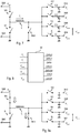
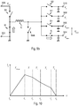
- Figures 9a and 9b show two exemplary switching states of the converter of Figure 7 and Figure 10 shows a possible waveform of the current I L flowing through the inductor L.
- the control circuit 32 closes at an instant t 0 and for a charge time T charge the switches Sh and Sbb and maintains opened the other switches (see Figure 9a ). Accordingly, during this phase the inductor L is connected to the supply voltage V bat and the current I L increase substantially linearly.
- the control circuit 32 opened the switches Sh and Sbb, and closes the switch Sl and one of the output switches S+, S-, S1 or S2 associated with the outputs, such as the switch S- (see Figure 9b ) . Accordingly, during a following time interval T - the inductor current I L flows to the output 304 and the voltage V float- increase, while the current I L decrease substantially linearly.
- the control circuit 32 opened the previously closed output switch, e.g. the switch S-, and closes a next output switch, such as the switch S+. Accordingly, during a following time interval T + the inductor current I L flows to the output 306 and the voltage V float+ increase, while the current I L decrease substantially linearly.
- the control circuit 32 opened the previously closed output switch, e.g. the switch S+, and closes a next output switch, such as the switch S1. Accordingly, during a following time interval T 1 the inductor current I L flows to the output 308 and the voltage V 1 increase, while the current I L decrease substantially linearly.
- the control circuit 32 opened the previously closed output switch, e.g. the switch S1, and closes a next output switch, such as the switch S2. Accordingly, during a following time interval T 2 the inductor current I L flows to the output 310 and the voltage V 2 increase, while the current I L decrease substantially linearly.
- the control circuit 32 opened the previously closed output switch, e.g . the switch S2.
- the sequence of the various discharge phases T + , T - , T 1 and T 2 may also be different, and the converter may use more or less phases in order to provide more or less output voltages.
- the control circuit 32 may start a new cycle T charge at a fixed frequency or immediately with the instant t 5 .
- the former being usually referred to as Pulse Width Modulation (PWM) mode, while the latter is usually called quasi resonant mode.
- PWM Pulse Width Modulation
- control circuit 32 apart from regulating the durations of the various discharge phases, the control circuit 32 also regulates the duration of the charge phase T charge in order to ensure that sufficient energy is stored in the inductor L in order to reach the requested output voltages.
- control circuit 32 may use for this purpose the voltage at the output terminal corresponding to the last discharge phase, e.g. the voltage V 2 terminal 310.
- control circuit 32 may increase the duration of the charge phase T charge when:
- control circuit 32 may decrease the duration of the charge phase T charge when:
- the control circuit 32 may use a fixed reference values for the voltages V 1 and V 2 , thereby provided substantially constant voltages V 1 and V 2 .
- the control circuit 32 may use variable reference values for the voltages V float+ and V float- determined as a function of the voltage V bat , thereby provided variable voltages V float+ and V float- , wherein the voltage V float between the terminals 304 and 306 is substantially constant (as described in the foregoing).
- the converter may use also a plurality of charge phases, e.g. a respective charge phase for each discharge phase.
- the electronic converter 30a may be operated as a convention buck-boost converter, wherein a plurality of outputs is regulated sequentially. Accordingly, in the embodiment considered, the electronic converter 30a is used in a time-sharing mode, wherein the switches Sh, Sl and Sbb and the inductor L are sequentially used to provide power to one of the output capacitors (by closing one of the switches S-, S+, S1 or S2).
- the electronic converter 30a could also generate only the voltages V float+ and V float- .
- the control circuit 32 may operate the switches in order to implement other converter topologies, which control the current flowing through the inductor L, such as:
- the control circuit 32 operates at least for these voltages the converter 30a as buck-boost converter as described in the foregoing.
- the solution described in the foregoing is a valid solution in order to generate constant or almost constant output voltage, e.g. the voltages V 1 and V 2
- the solution may present some drawbacks for the generation of variable voltages, such as the voltages V float + and V float- .
- the supply voltage V bat and thus the reference voltage V ref may vary fast ( ⁇ 2 ms).
- the electronic converter 30a should be able to provide also voltages V float + and V float- , which are able to follow these variations.
- the architecture shown in Figure 7 requires the tank/output capacitors C+ and C-, which are charged by the current I L .
- the converter is operated sequentially with the time-sharing technique.
- the output capacitors may not be too small.
- the capacitances of the capacitors C1 and C2 may be between 5 e 100 uF, e.g. approximately 10 uF.
- large charge or discharge currents would be required, which would render the system less efficient.
- V float+ and V float- are regulated independently.
- two separate control loops are required, and these loops have to ensure a sufficient precision in order to obtain the requested voltage V float .
- FIG 11 shows thus a second embodiment of the electronic converter 30a.
- the electronic switch S-associated with the terminal 304 providing the voltage V float- is not connected anymore to the second terminal of the inductor L, but to the first terminal of the inductor L, i.e. the intermediate point between the switches Sh and Sl of the half-bridge.
- a single capacitor Cf is connected between the terminals 304 and 306.
- the capacitors C+ and C- are thus omitted.
- Figure 13 shows again a possible waveform of the current I L flowing through the inductor L
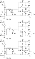
- Figures 14a, 14b and 14 show various switching stages of the converter 30a.
- control circuit 32 closes again at an instant t 0 and for a charge time T charge the switches Sh and Sbb and maintains opened the other switches (see Figure 14a ). Accordingly, during this phase the current I L increase substantially linearly. At an instant t 1 , the control circuit 32 opens thus the switches Sh and Sbb and the charge phase ends.
- the control circuit 32 drives the control terminal of the switches S+ and S- in order to close these switches, e.g. at the instant t 1 (see Figure 14b ). Accordingly, in this embodiment, the switches S+ and S- are closed during the same phase.
- the control circuit 32 may thus generate (in addition to the drive signals DRVh, DRVl, DRVbb, DRV1 and DRV2 configured to drive the switches Sh, Sl, Sbb, S1 and S2, respectively) a common drive signal DRVf, which drives simultaneously the switches S+ and S-.
- the control circuit 32 receives at input directly the voltage difference V float .
- the inductor current I L will flow from the terminal 304 to the terminal 306, thereby charging the capacitor Cf.
- the voltage V float- will decrease and the voltage V float- will increase, whereby the V float between the terminals 304 and 306 will increase.
- the current I L decrease substantially linearly and the control circuit 32 may switch off the switches S+ and S- at an instant t 3 directly when the voltage V float reaches the requested constant value.
- these switches should support the mentioned current flow direction, i.e.
- the switch S- should be configured to permit a current flow from the terminal 304 towards the first terminal of the inductor L (as a function of the respective drive signal DRV- / DRVf ) and the switch S+ should be configured to permit a current flow from the second terminal of the inductor L towards the terminal 306 (as a function of the respective drive signal DRV+ / DRVf) .
- the control circuit 32 opened the previously closed output switches S+ and S-, and closes the switch Sl and one of the other output switches, such as the switch S1 (see Figure 14c ). Accordingly, as in the previous embodiment, during a following time interval T 1 the inductor current I L flows now from ground GND (via the switches Sl an S1) to the output 308 and the voltage V 1 increase, while the current I L decrease substantially linearly.
- the control circuit 32 opened the previously closed output switch, e.g. the switch S1, and closes a next output switch, such as the switch S2. Accordingly, during a following time interval T 2 the inductor current I L flows to the output 310 and the voltage V 2 increase, while the current I L decrease substantially linearly.
- the control circuit 32 opened the previously closed output switch, e.g. the switch S2.
- the sequence of the various discharge phases T + / - , T 1 , and T 2 may also be different, and the converter may use more or less phases in order to provide more or less output voltages.
- a plurality of charge phase may be used, such as a respective charge phase for each discharge phase.
- both switches S+ and S- are closed (while the other switches Sh, Sl, Sbb, S1 and S2 are opened).
- the inductor current I L charges the capacitor Cf and the control circuit may directly regulate the output voltage V float .
- the switch Sl and/or the switch connected to the output terminal providing the highest output voltage may also be implemented with a diode, and the control unit 302 may thus not generate the respective drive signals, e.g . the drive signal DRVl for the switch Sl and the drive signal DRV2 for the switch S2.
- the control circuit 32 regulates only the voltage difference between the terminals 304 and 306, i.e. the voltage V float . However, the control circuit 32 does not regulate the offset of the voltages V float+ and V float- with respect to ground GND.
- control circuit 32 could thus also regulate the voltages V float+ and V float- with respect to ground GND.
- the control circuit 32 could close both switches S+ and S- until either the voltage V float+ or the voltage V float- reaches the requested reference value (V ref +/- V float /2), and then either:
- Figure 15 shows an embodiment, which permits a simplified control of voltage offset of the voltages V float+ and V float- .
- the control circuit 32 regulates the duration of the interval T + / - in order to obtain the requested voltage difference V float (as described with respect to Figures 11-14 ), however, the control circuit 32 does not regulate the voltage V float+ and V float- with respect to ground GND.
- the offset of these voltage V float+ and V float- is imposed separately by coupling the terminals 302 and 304 to the reference voltage V ref , representing a common mode for the terminals 302 and 304.
- the converter 30a may thus comprise a circuit 34 configured to generate the voltage V ref at a node/terminal 312 as a function of the voltage V bat .
- the circuit 34 comprises a resistive voltage divider comprising two resistors Rref1 and Rref2 connected (e.g. directly) between the terminals 300 and 302. Accordingly, in the embodiment considered, the voltage V ref at the intermediate point between the two resistors Rref1 and Rref2 (representing the node/terminal 312 in the embodiment considered) will be proportional to the supply voltage V bat based on the values of the resistors Rref1 and Rref2.
- the resistors Rref1 and Rref2 have substantially the same value.
- the circuit 34 may also comprise more complex circuits for implementing a reference voltage generator, possibly comprising also amplifier stages (such as one or more operation amplifiers and/or current mirrors) in order to ensure a stable output voltage V ref for different load conditions at the node/terminal 312.
- the terminals 304 and 306 are coupled to the voltage V ref via respective resistors Rcm1 and Rcm2, i.e. a resistor Rcm1 is connected (e.g. directly) between the terminal 306 and the terminal 312 providing the voltage V ref (e.g. the intermediate point between the resistors Rref1 and Rref2) and a resistor Rcm2 is connected (e.g. directly) between the terminal 304 and the terminal 312.
- the resistors Rcm1 and Rcm2 should have the same value.
- the resistors could also have different values, e.g. when a different scaling with respect to the ground GND is requested.
- the inductance of the inductor L may be 10 uH (micro-henry)
- the capacitance of the capacitor Cf may be 10 uF (micro-farad)
- the resistances of the resistors Rcm1 and Rcm2 may be 10 kOhm (kilo-ohm)
- the resistances of the resistors Rref1 and Rref2 may be 10kOhm.
- the inductor L, the capacitor Cf and the resistors Rcm1, Rcm2, Rref1 and Rref2 have values in the micro-henry/micro-farad/kilo-ohm range, respectively.
- the inventors have observed that the solution described with respect to Figures 15 and 16 is a valid solution, in particular when no high precision of the offsets V float+ and V float- with respect to the ground GND is required. From a practical point of view, the circuit will however comprise also parasitic capacitance, such as capacitances associated with the first and second terminal of the inductor L.
- these parasitic currents I par1 and I par2 would not represent any particular issue, when their amplitude would be the same. However, in case the values are different, a current ( I par1 - I par2 ) will also flow towards the node 312 providing the reference voltage V ref .
- the reference voltage V ref is provided by a voltage divider (see Figure 16 ), this current will vary the reference voltage V ref from the requested value.
- Figure 18 shows thus a modified embodiment, which permits to inhibit or at least reduce this current flow towards the node 312.
- the electronic converter 30a comprises (in addition to the components described with respect to Figure 15 ) at least one of:
- the capacitors Cf1 and Cf2 may have a capacitance being significantly smaller than the capacitance of the capacitor Cf, such as less than 5%, preferably between 0.1% and 2%, preferably approximately 1%.
- the capacitance of the capacitors Cf1 and Cf2 is between 10 and 100 nF (nano-farad).
- the capacitors Cf1 and Cf2 may have the same capacitance.
- the parasitic currents I par1 and I par2 will also flow, however, the current pulse ( I par1 - I par2 ) will not flow (or will flow less) towards the node 312 but through the low impedance path provided by the capacitor Cf1 and/or the capacitor Cf2 (and also the capacitor Cf).
- the capacitors Cf1 and/or Cf2 may be connected to any reference voltage having a low impedance towards ground GND (as it is the case for the supply voltage V bat ).
- the capacitors Cf1 may also be connected to the terminal 302 (instead of the terminal 300) and/or the capacitors Cf2 may also be connected to the terminal 300 (instead of the terminal 302) .
- Figure 19 shows a second embodiment for obtaining the voltage offsets V float+ and V float- with respect to ground GND.
- the embodiment is based on the circuit shown in Figure 11 and comprises in addition two further circuits:
- the first clamp circuit 36 is configured to selectively permit a current flow towards the terminal 306 until the voltage corresponds to an upper voltage threshold V H .
- the clamp circuit 36 may comprise a transistor 362, such as a n-channel FET, such as a NMOS, connected ( e.g . directly) between the terminal 300 providing the supply voltage V bat and the terminal 306.
- a transistor 362 such as a n-channel FET, such as a NMOS, connected ( e.g . directly) between the terminal 300 providing the supply voltage V bat and the terminal 306.
- the gate terminal of the transistor 362 is driven by an operational amplifier 364.
- the operational amplifier receives at the non-inverting/positive input terminal the upper voltage threshold V H and at the inverting/negative input terminal the voltage at the terminal 306.
- the circuit 36 will drive the transistor 362 thereby permitting a current flow (from the supply voltage V bat ) towards the terminal 306, until the voltage at the terminal 306 reaches or is greater than the voltage V H .
- the second clamp circuit 38 is configured to selectively permit a current flow from the terminal 304 until the voltage corresponds to a lower voltage threshold V L .
- the clamp circuit 38 may comprise a transistor 382, such as a p-channel FET, such as a PMOS, connected ( e.g. directly) between the terminal 304 and the terminal 302 (ground GND) .
- a transistor 382 such as a p-channel FET, such as a PMOS
- the gate terminal of the transistor 382 is driven by an operational amplifier 384.
- the operational amplifier receives at the non-inverting/positive input terminal the lower voltage threshold V L and at the inverting/negative input terminal the voltage at the terminal 304.
- the circuit 38 will drive the transistor 382 thereby permitting a current flow from the terminal 304 (towards ground GND), until the voltage at the terminal 304 reaches or is smaller than the voltage V L .
- the clamp circuits 36 and 38 are not used to directly impose the voltages V ref +/- V float /2, but the clamp circuits set only approximately the voltages at the nodes 304 and 306 with respect to ground GND.
- control unit 32 drives the switches of the converter 30a, the control unit 32 will also regulate the voltage difference V Diff until the value corresponds to the requested value V float .
- the clamp circuits 36 and 38 do not intervene during this regulation of the voltage difference V Diff .
- the clamp circuits 34 and 36 may absorb the current peaks generated by the parasitic current mentioned before and/or may intervene when the supply voltage V bat varies.
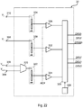
- Figure 22 shows in this respect a possible embodiment of the control circuit 32.
- the voltages V float+ and V float- are provided to a differential amplifier 320, e.g. based on an operation amplifier.
- the output of the differential amplifier 320 is connected to an error amplifier 324, such as a PI (Proportional-Integral) or PID (Proportional-Integral-Derivative) regulator, configured to generate an error signal as a function of the voltage difference and a reference signal REF.
- a scaling circuit and/or a current-voltage conversion circuit 322, such as a voltage divider comprising two resistors may be connected between the differential amplifier 320 and the error amplifier 324.
- the optional voltages V 1 and V 2 may be provided similarly to respective error amplifiers 332 and 336. While also in this case may be used scaling circuit 330 and 334, usually no differential amplifiers are required, because the voltages V 1 and V 2 are referred to ground GND.
- the error signals at the output of the error amplifiers 324, 332 and 336 are provided to a driver circuit 326.
- the driver circuit 326 is configured to manage the charge phase and the various discharge phases by generating the drive signals for the switches Sh, Sl, Sbb, S+, S- S1 and S2.
- the drive signal DRVl for the switch Sl and the drive signal DRV2 for the switch S2 are purely optional, because these switches may also be implemented with diodes.
- the driver circuit 326 may be a Pulse-Width-Modulation driver circuit.
- the driver circuit 326 may have associated an oscillator 328 configured to generate an oscillator signal having a fixed frequency, i.e. a fixed switching period T SW .
- the driver circuit 326 sets the drive signals DRVh and DRVbb for closing the switches Sh and Sbb.
- the driver circuit 326 sets the drive signals DRVh and DRVbb for opening the switches Sh and Sbb.
- these drive signals DRVh and DRVbb are PWM signals, which are set:
- the driver circuit 326 sets then ( e.g . at the instant t 1 ) the drive signal DRVf for closing the switches S+ and S-.
- the driver circuit 326 sets the drive signal DRVf for opening the switches S+ and S-.
- the drive signal DRVf is a PWM signal, which is set:
- the driver circuit 326 sets then ( e.g . at the instant t 3 ) the drive signal DRV1 for closing the switch S1 (and possibly the drive signal DRVl for closing the switch Sl).
- the driver circuit 326 sets the drive signal DRV1 for opening the switch S1.
- the drive signal DRV1 is a PWM signal, which is set:
- the driver circuit 326 may then generate the drive signal DRV2 for the switch S2.
- the switch S2 is implemented with a diode. Accordingly, when the switches S+, S- and S1 are opened, the current I L will flow through the diode S2 towards the terminal 310 until the current I L reaches zero or the switching duration T SW has finished.
- the driver circuit 326 is configured to vary the switch-on durations T + / - and T 1 of the drive signals DRVf and DRV1 as a function of the error signals provided by the error amplifiers 324 and 332, respectively. Specifically, in the embodiment considered, the error amplifiers 324 and 332 will vary these durations (via the respective error signals) until the voltages V float and V 1 correspond to the respective requested values.
- the driver circuit 326 is configured to vary the switch-on duration T charge of the drive signals DRVh and DRVbb as a function of the error signal provided by the error amplifiers 336. Specifically, in the embodiment considered, the error amplifier 336 will vary the duration (via the respective error signal), thereby varying the maximum current I L , until the voltages V 2 correspond to the respective requested values. Additionally, the driver circuit 326 may vary the switch-on duration T charge also as a function of the error signals provided by the other error amplifiers, e.g. the amplifiers 324 and 332, which may be useful in order to perform a (predictive) control in case of short load variations of the outputs. For example, such an arrangement is useful when the error amplifiers 324, 332 and 336 have (in addition to an integral component) a proportional and/or derivative component.
- control unit 32 is configured to manage the following phases which are repeated periodically:
- the discharge phase T + / - may be the last discharge phase or an intermediate discharge phase.
- control unit is configured to stop an intermediate phase when the respective output voltage reaches the requested value.
- last discharge phase is used to control the duration of the charge phase T charge .
- control unit 32 may:
- control unit 32 may:
- the term integrated circuit does not imply that the die is mounted within a package, but e.g. the die could also be mounted directly on a printed-circuit-board (PCB).
- PCB printed-circuit-board
- the term pad is used to identify the pad of the die of the integrated circuit and the term pin identifies the pin or lead of an optional external package of the integrated circuit.
- pad/pin this indicates that the die has a pad and in case an external package is used, also the package has a corresponding pin, which is connected to the respective
- Figure 23 shows an embodiment, wherein such integrated circuit may comprise:
- the integrated circuit does not comprise large inductors, capacitors and resistors, such as the inductor L, the capacitor Cf, and the capacitors C1 and C2, i.e. these components are external with respect to the integrated circuit.
- small capacitors such as the capacitors Cf1 and Cf2, and the various resistors described may be external or internal.
- the integrated circuit comprises:
- the capacitor Cf may be connected directly to two pads/pins 304 and 306.
- Figure 23 shows an embodiment wherein four pins/pads 304, 306, 404 and 406 are used. Specifically, the pins/pads 404 and 406 are connected directly to the switches S- and S+, respectively. Conversely, the pins/pads 304 and 306 provide the voltages V foat- and V float+ .
- a first terminal of an external capacitor Cf may be connected to the pins/pads 304 and 404, thereby connecting the pin/pad 304 externally to the pin/pad 404, and a second terminal of the external capacitor Cf may be connected to the pins/pads 306 and 406, thereby connecting the pin/pad 306 externally to the pin/pad 406.
- this embodiment has the advantage that the parasitic inductances Lbond1, Lbond2, Lbond3 and Lbond4 of the bonding of the pins 304, 306, 404 and 404 implement with the capacitor Cf an improved filter stage for current peaks.
- the integrated circuit comprises also the clamp circuits 38 and 36 which are connected internally to the pins/pads 306 and 304.
- the electronic converter comprises the capacitors Cf1 and Cf2, which are connected externally to the pins/pads 304/404 and 306/406, respectively.
- the electronic converter could also comprise the coupling resistors Rcm1 and Rcm2, which may be connected externally in parallel to the capacitor Cf or internally between the pins/pads 304/306 or 404/406.
- the same electronic converter 30a may be used to generate in addition to the voltage V float also one or more additional voltages V 1 and V 2 . In case these voltages are absent, the respective switches S1 and S2, and also the switch/diode Sl may be omitted.
Landscapes
- Engineering & Computer Science (AREA)
- Power Engineering (AREA)
- Microelectronics & Electronic Packaging (AREA)
- Multimedia (AREA)
- Mechanical Engineering (AREA)
- Physics & Mathematics (AREA)
- Acoustics & Sound (AREA)
- Signal Processing (AREA)
- Dc-Dc Converters (AREA)
- Input Circuits Of Receivers And Coupling Of Receivers And Audio Equipment (AREA)
- Signal Processing Not Specific To The Method Of Recording And Reproducing (AREA)
- Amplifiers (AREA)
Abstract
Description
- Embodiments of the present disclosure relate to electronic converters. Specifically, various embodiments of the present disclosure relate to electronic converters for audio systems, such as class D audio amplifiers.
-
Figure 1 shows a typical audio system. In the example considered, the system comprises anaudio signal generator 10, such as a radio, CD o MP3 player, generating an analog audio signal AS to be sent to at least one speaker SPK. - In the example considered, an
audio amplifier 20 is connected between theaudio signal generator 10 and the speaker SPK, which is configured to generate an amplified audio signal AAS by amplifying the analog audio signal AS provided by theaudio signal generator 10. - For example,
Figure 2 shows a possible implementation of a so-called classD audio amplifier 20. Specifically, in the example considered, theaudio amplifier 20 comprises awaveform generator 202 generating a periodic triangular waveform signal TS, having typically a frequency between 250kHz and 2.5MHz. The triangular waveform signal TS is sent together with the audio signal AS to acomparator 204, which compares the audio signal AS with the triangular waveform signal TS thereby generating a square wave signal DS, whose duty-cycle varies as a function of the amplitude of the audio signal AS. The square wave signal DS is then amplified by anamplifier stage 206, thereby generating an amplified square wave signal ADS. - For example,
Figure 3 shows an example of theamplifier stage 206, which comprises a half-bridge comprising two electronic switches SW1 and SW2, such as (n-channel) Field Effect Transistors (FET), connected in series between twoterminals terminal 212 represent a ground GND. In the example considered, the control terminals of the switches SW1 and SW2 (e.g., the gate terminals of respective transistors) are driven as a function of the digital signal DS. For example, in the example considered are shown twodriver circuits control circuit 2060 configured to generate the control signals for thedriver circuits amplifier 206 is configured to convert the amplitude of the digital signal DS to the value of the voltage received at theterminals - Finally, the amplified square wave signal ADS is sent to a low-pass or
bandpass filter 208, which removes at least the high-frequency spectrum from the amplified signal square wave signal ADS, thereby generating an amplified audio signal AAS, which is proportional to the original audio signal AS. - For example,
Figure 4 shows an example aLC filter 208. Generally, thefilter stage 208 comprises two input terminals for receiving the signal ADS provided by theamplifier stage 206, e.g. the input terminals are connected the intermediate point of the half-bridge and the ground GND shown inFigure 3 . Moreover, thefilter stage 208 comprises two output terminals for connection to the speaker SPK. Specifically, in the example considered, the first input terminal is connected to the first output terminal via an inductor L, and the second input terminal and the second output terminal are short circuited to ground GND. Finally, a capacitance C is connected in parallel with the output, i.e. between the output terminals. Substantially similar (active or passive) low-pass orbandpass filters 208 are provided in most audio amplifier circuits and/or may be integrated also within the speaker SPK. - Accordingly, a class D amplifier is based on the fact that the switching frequency of the
amplifier 20 is significantly higher than the usual audio band (between 20 Hz and 20kHz) and accordingly the high switching frequency may be filtered with thefilter stage 208, thereby reconstructing the profile of the original audio signal AS. - In the context of digital audio data, the
signal generator 10 may comprise an analog-to-digital converter for generating the signal AS or thesignal generator 10 may provide directly the digital signal DS. Accordingly, theblocks - Generally, the audio system may also use a plurality of speakers SPK, such as two or four, with
respective audio amplifiers 20 using different signals AS/DS. - Those of skill in the art will appreciate that the audio system usually comprises also one or more
electronic converters 30 configured to generate the regulated supply voltages for the various blocks of the audio system, such as the supply voltage for theaudio signal generator 10 and possibly theblocks control circuit 2060 and thedriver circuits - For example, usually the
converter 30 comprises a DC/DC converter, such as a converter configured to convert the voltage Vbat into a lower supply voltage, such as a voltage between 1.5 and 3.3 VDC, e.g. 1.8 VDC, used by the digital circuits of the audio system and/or the low power analog processing circuits. Similarly, additional regulated voltages may be generated for thedriver circuits driver circuit 2064. - In case of a car radio, the design of the various components of the audio system may be challenging, because of the large variations of voltage Vbat of the automotive battery. For example, during crank and dump, a typical battery voltage of 14.4V may sharply (in less than 2 ms) drop down to 4-5V or rise up to 40V. For a proper operation, the
electronic converter 30 should thus be able to control the supply voltages of the audio system for all battery conditions. - In view of the above, it is an objective of the various embodiments of the present disclosure to provide solutions for generating a regulated voltage.
- According to one or more embodiments, one or more of the above objectives is achieved by means of an electronic converter having the features specifically set forth in the claims that follow. Embodiments moreover concern a related audio system, integrated circuit and method of operating an electronic converter.
- The claims are an integral part of the technical teaching of the disclosure provided herein.
- As mentioned before, various embodiments of the present disclosure relate to an electronic converter, such as an electronic converter for an audio amplifier
- In various embodiments, the electronic converter comprises two input terminals configured to receive a supply voltage and two output terminals configured to provide a regulated voltage.
- In various embodiments, the electronic converter comprises an inductor comprising a first and a second terminal. A first electronic switch is connected between the first input terminal and the first terminal of the inductor. A second electronic switch is connected between the second terminal of the inductor and the second input terminal.
- In various embodiments, the electronic converter comprises moreover, a third electronic switch connected between the second terminal of the inductor and the first output terminal and a fourth electronic switch is connected between the first terminal of the inductor and the second output terminal. A capacitor is connected between the first output terminal and the second output terminal.
- In various embodiments, a control circuit monitors the voltage between the two output terminals. During a charge phase, the control circuit closes the first and the second electronic switch, thereby increasing the current flowing through the inductor. During a discharge phase, the control circuit closes the third and the fourth electronic switch, whereby the current flowing through the inductor charges the capacitor, thereby increasing the voltage between the two output terminals.
- In various embodiments, the control circuit regulates the duration of the charge phase and/or the discharge phase, such that the voltage between the two output terminals corresponds to a requested value. For example, the control circuit may determine whether, at the end of the discharge phase, the voltage between the two output terminals is greater than the requested value. When, at the end of the discharge phase, the voltage between the two output terminals is smaller than the requested value, the control circuit may increase the duration of the charge phase. Conversely, when, at the end of the discharge phase, the voltage between the two output terminals is greater than the requested value, the control circuit may decrease the duration of the charge phase.
- Generally, the electronic converter may also comprise one or more further outputs. For example, in various embodiments, the electronic converter comprises a further output terminal configured to provide a further regulated voltage, wherein the further regulated voltage is referred to the second input terminal, which represents a ground. A further capacitor is connected between the further output terminal and the second input terminal, wherein a further electronic switch is connected between the second terminal of the inductor and the further output terminal. In this case, the converter comprises also a fifth electronic switch connected between the first terminal of the inductor and the second input terminal. Generally, the fifth electronic switch and/or the further electronic switch may be implemented with diodes.
- In this case, the control circuit may thus also regulate the further output voltage. For example, during a further discharge phase, the control circuit may close the fifth and the further electronic switch, whereby the current flowing through the inductor charges now the further capacitor, thereby increasing the voltage between the further output terminal and the second input terminal. Similarly, the control circuit may regulate the duration of the charge phase and/or the further discharge phase, such that the voltage between the further output terminal and the second input terminal corresponds to a further requested value.
- For example, in various embodiments, the control circuit is configured for repeating periodically the charge phase, the discharge phase and the further discharge phase, wherein one of the discharge phases corresponds to a last discharge phase and the other of the discharge phases corresponds to an intermediate discharge phase between the charge phase and the last discharge phase.
- In this case, the control circuit may stop the intermediate discharge phase when the respective voltage being increased during the intermediate discharge phase reaches the respective requested value. Moreover, the control circuit may increase the duration of the charge phase when, at the end of the last discharge phase, the respective voltage being increased during the last discharge phase is smaller than the respective requested value, and decrease the duration of the charge phase when, at the end of the last discharge phase, the respective voltage being increased during the last discharge phase is greater than the respective requested value.
- Generally, the electronic converter may also control the offset of the voltage between the two output terminals with respect to the second input terminal, i.e. with respect to ground.
- For example, in various embodiments, the electronic converter comprises a reference voltage generator, such as a voltage divider, configured to generate a reference voltage being preferably proportional to the supply voltage. In this case, a first resistor may be connected between the first output terminal and the reference voltage, and a second resistor may be connected between the second output terminal and the reference voltage.
- In various embodiments, the electronic converter may also be configured to filter parasitic current spikes. For this purpose, the electronic converter may comprise a first capacitor connected between the first output terminal, and the first input terminal or the second input terminal. Additionally or alternatively, the electronic converter may comprise a second capacitor connected between the second output terminal, and the first input terminal or the second input terminal.
- Generally, in addition or as alternative to the coupling to the reference voltage, the converter may also comprise clamp circuits for limiting the voltage offset of the two output terminals with respect to the second input terminal, i.e. with respect to ground. Specifically, the electronic converter may comprise a first clamp circuit configured to selectively permit a current flow towards the first output terminal, until the voltage between the first output terminal and the second input terminal reaches or is greater than an upper voltage. The electronic converter may comprise also a second clamp circuit configured to selectively permit a current flow from the second output terminal, until the voltage between the second output terminal and the second input terminal reaches or is smaller than a lower voltage.
- Embodiments of the present disclosure will now be described with reference to the annexed drawings, which are provided purely by way of non-limiting example and in which:
-
Figures 1, 2, 3 and4 have already been described in the foregoing; -
Figure 5 shows an embodiment of an electronic converter configured to generate a regulated voltage in accordance with the present disclosure; -
Figure 6 shows an exemplary waveform of the regulated voltage generated by the electronic converter ofFigure 5 ; -
Figure 7 shows a first embodiment of the electronic converter ofFigure 5 ; -
Figure 8 shows an embodiment of a control circuit of the electronic converter ofFigure 7 ; -
Figures 9a and9b show possible switching states of the electronic converter ofFigure 7 ; -
Figure 10 shows a waveform of the behavior of the electronic converter ofFigure 7 ; -
Figure 11 shows a second embodiment of the electronic converter ofFigure 5 ; -
Figure 12 shows an embodiment of a control circuit of the electronic converter ofFigure 11 ; -
Figure 13 shows a waveform of the behavior of the electronic converter ofFigure 11 ; -
Figures 14a, 14b and 14c show possible switching states of the electronic converter ofFigure 11 ; -
Figure 15 shows a third embodiment of the electronic converter ofFigure 5 ; -
Figure 16 shows an embodiment of a reference voltage generator for the electronic converter ofFigure 15 ; -
Figures 17 show details of the parasitic behaviors of the electronic converter ofFigure 15 ; -
Figure 18 shows a fourth embodiment of the electronic converter ofFigure 5 ; -
Figure 19 shows a fifth embodiment of the electronic converter ofFigure 5 ; -
Figures 20 and 21 show embodiments of clamp circuits for the electronic converter ofFigure 19 ; -
Figure 22 shows an embodiment of a control circuit for the electronic converters ofFigures 11 ,15 ,18 and19 ; and -
Figure 23 shows a sixth embodiment of the electronic converter ofFigure 5 . - In the following description, numerous specific details are given to provide a thorough understanding of embodiments. The embodiments can be practiced without one or several specific details, or with other methods, components, materials, etc. In other instances, well-known structures, materials, or operations are not shown or described in detail to avoid obscuring aspects of the embodiments.
- Reference throughout this specification to "one embodiment" or "an embodiment" means that a particular feature, structure, or characteristic described in connection with the embodiment is included in at least one embodiment. Thus, the appearances of the phrases "in one embodiment" or "in an embodiment" in various places throughout this specification are not necessarily all referring to the same embodiment. Furthermore, the particular features, structures, or characteristics may be combined in any suitable manner in one or more embodiments.
- The headings provided herein are for convenience only and do not interpret the scope or meaning of the embodiments.
- In the following
Figures 5 to 23 parts, elements or components which have already been described with reference toFigures 1 to 4 are denoted by the same references previously used in such Figures; the description of such previously described elements will not be repeated in the following in order not to overburden the present detailed description. - As mentioned before, various embodiments of the present application relate to an
electronic converter 30a, such as anelectronic converter 30a for an audio system (see also the description ofFigures 1 to 4 ). -
Figure 5 shows the general architecture of an embodiment of theelectronic converter 30a. Generally, theelectronic converter 30a comprises twoinput terminals negative terminal 302 represent a ground GND. For example, theterminals - In the embodiment considered, the
electronic converter 30a comprises at least twooutput terminals signal generator 10, and/or theblocks control circuit 2060 described in with respect toFigure 2 . - Specifically, in various embodiments, the voltage at the terminal 304 is not connected directly to ground GND, i.e. the voltage V float- between the (negative) terminal 304 and ground GND is not zero. However, the
electronic converter 30a is configured to generate a regulated and substantially constant voltage Vfloat between theterminals - Specifically, in various applications it may be desirable that the voltage Vfloat is referred to a reference voltage Vref , which is smaller than the voltage Vbat , i.e.:

- Specifically, in various embodiments, the
converter 30a generates a voltage Vfloat+ between thepositive terminal 306 and ground GND, which corresponds to:
negative terminal 304 and ground GND which corresponds to:
- For example, in various embodiments, the reference voltage Vref is variable and set to 50% of the supply voltage Vbat (or generally Vref = x * Vbat , with 0 < x < 1). For example, the reference voltage Vref may be provided by an additional voltage regulator or a voltage divider.
- Generally, such a floating voltage Vfloat may be useful in many applications.
- For example, in the case of an audio system, such a floating voltage Vfloat may be used by the analog circuits, in particular by the
circuit 2060, in order to improve the quality of the audio signal, in particular with respect to the signal/noise ratio. For example, this simplifies the implementation of unity-gain amplifier as described e.g. in documents Maxim, "APPLICATION NOTE 3977 - Class D Amplifiers: Fundamentals of Operation and Recent Developments", Jan 31, 2007, available at https://www.maximintegrated.com/en/app-notes/index.mvp/id/3977, orUS 8,558,618 B2 , which are incorporated herein by reference, because the voltage gain of theamplifier stage 206 is unitary. Similarly, also the digital circuits may work with the floating voltage Vfloat in order to simplify the interface between the digital and analog circuits. - For example,
Figure 6 shows exemplary waveform for the supply voltage Vbat , the reference voltage Vref and the voltages Vfloat+ and Vfloat- (referred to ground GND) . - As mentioned before, in case the
converter 30a is powered via a vehicle battery BAT, the variation of the supply voltage Vbat may be fast (< 2ms). In various embodiments, theconverter 30a should thus be able to generate voltages Vfloat+ and Vfloat- following such voltage variations. For example, this implies that the capacitances associated with theterminals - In various embodiments (see e.g.
Figure 5 ), theelectronic converter 30a may also comprise one or more additional output terminals, such asterminals driver circuits 2062 and 2054 arranged to drive the switches of a half-bridge. Generally, only a single terminal may be required for these voltages V1 and V2 , insofar as these voltages may be referred to ground GND. - Accordingly, in various embodiments, the
converter 30a receives at input a variable input voltage Vbat and provides at output one or more voltages, which generally may be smaller or greater than the input voltage Vbat . Thus, generally, a plurality of electronic converters may be used, wherein each electronic converter is configured to generate a respective one of the voltages Vfloat+ , Vfloat- , V1 and V2. - Conversely
Figure 7 shows an embodiment of anelectronic converter 30a configured to generate a plurality of the voltages Vfloat+ , Vfloat- , V1 and V2. - Specifically, in the embodiment considered a so called Single-Inductor Multiple-Output (SIMO) architecture is used. As the term implies, in this case, the
electronic converter 30a comprises a single inductor L. - Specifically, in the embodiment considered, the
electronic converter 30a comprise a half-bridge comprising two electronic switches Sh and Sl, such as (e.g. n-channel) FETs, connected (e.g. directly) in series between theterminals terminals - In the embodiment considered, a first terminal of the inductor L is connected (e.g. directly) to the intermediate point between the switches Sl and Sh. The second terminal of the inductor L is connected (e.g. directly) via a further electronic switch Sbb to the
negative terminal 302. Moreover, the second terminal of the inductor L is also connected (e.g. directly) via a respective switch, such as a (e.g. n-channel) FET, to each of the output terminals of theelectronic converter 30a, i.e. theterminals optional terminals 308 and/or 310 For example, in the embodiment considered, theelectronic converter 30a comprises: - an electronic switch S- connected (e.g. directly) between the second terminal of the inductor L and the terminal 304 providing the voltage Vfloat- ;
- an electronic switch S+ connected (e.g. directly) between the second terminal of the inductor L and the terminal 306 providing the voltage Vfloat+ ;
- optionally an electronic switch S1 connected (e.g. directly) between the second terminal of the inductor L and the terminal 306 providing the voltage V1 ; and
- optionally an electronic switch S2 connected (e.g. directly) between the second terminal of the inductor L and the terminal 308 providing the voltage V2.
- In various embodiments, each of the switches S-, S+, S1 and S2 may ensure that current may flow form the second inductor terminal towards the respective output terminal. For this purpose, each of the switches may be:
- a bidirectional switch, e.g. by using two field effect transistors connected in opposite direction in series, e.g. in case of n-channel FET the drain of a first FET may be connected to the secondo inductor terminal, the drain of a second FET may be connected to the respective output terminal, and the source terminals of the two FETs may be connected together; or
- an unidirectional switch, e.g. by connecting a diode in series with a FET.
- Moreover, as will be described in the following, the electronic switch associate with the
output terminal driver circuit 2062, may also be implemented with a diode. - In the embodiment considered, a respective capacitor C+, C-, C1 and C2 is associated with each of the output terminals. Specifically, in the embodiment considered, each terminal 304, 306, 308 and 310 is connected (e.g. directly) via the respective capacitor C+, C-, C1 or C2 to ground GND.
- As shown in
Figure 8 , theelectronic converter 30a comprises also acontrol circuit 32 configured to generate drive signals DRVh, DRVl, DRVbb, DRV-, DRV+, DRV1 and DRV2 configured to drive the switches Sh, Sl, Sbb, S-, S+, S1 and S2, respectively, as a function of the output voltages Vfloat- , Vfloat+ , V1 and V2 , and the respective requested output voltages (not shown inFigure 8 ). - Generally, by driving the switches in an appropriate manner, the
converter 30a may be operated as buck (step-down), boost (step-up) or buck-boost converter. - For example, at the example of
Figures 9a ,9b and 10 will be described a possible operation of thecontrol circuit 32. Specifically,Figures 9a and9b show two exemplary switching states of the converter ofFigure 7 andFigure 10 shows a possible waveform of the current IL flowing through the inductor L. - In the embodiment considered, the
control circuit 32 closes at an instant t0 and for a charge time Tcharge the switches Sh and Sbb and maintains opened the other switches (seeFigure 9a ). Accordingly, during this phase the inductor L is connected to the supply voltage Vbat and the current IL increase substantially linearly. - At the end of the charge interval Tcharge , i.e. at an instant t1 , the
control circuit 32 opened the switches Sh and Sbb, and closes the switch Sl and one of the output switches S+, S-, S1 or S2 associated with the outputs, such as the switch S- (seeFigure 9b ) . Accordingly, during a following time interval T- the inductor current IL flows to theoutput 304 and the voltage Vfloat- increase, while the current IL decrease substantially linearly. - At an instant t2 , e.g. when the voltage Vfloat- has reached the requested value, the
control circuit 32 opened the previously closed output switch, e.g. the switch S-, and closes a next output switch, such as the switch S+. Accordingly, during a following time interval T+ the inductor current IL flows to theoutput 306 and the voltage Vfloat+ increase, while the current IL decrease substantially linearly. - At an instant t3 , e.g. when the voltage Vfloat+ has reached the requested value, the
control circuit 32 opened the previously closed output switch, e.g. the switch S+, and closes a next output switch, such as the switch S1. Accordingly, during a following time interval T1 the inductor current IL flows to theoutput 308 and the voltage V1 increase, while the current IL decrease substantially linearly. - At an instant t4 , e.g. when the voltage V1 has reached the requested value, the
control circuit 32 opened the previously closed output switch, e.g. the switch S1, and closes a next output switch, such as the switch S2. Accordingly, during a following time interval T2 the inductor current IL flows to theoutput 310 and the voltage V2 increase, while the current IL decrease substantially linearly. - At an instant t5 , e.g. when the voltage V2 has reached the requested value, the
control circuit 32 opened the previously closed output switch, e.g. the switch S2. - Generally, the sequence of the various discharge phases T+ , T- , T1 and T2 may also be different, and the converter may use more or less phases in order to provide more or less output voltages.
- The
control circuit 32 may start a new cycle Tcharge at a fixed frequency or immediately with the instant t5 . The former being usually referred to as Pulse Width Modulation (PWM) mode, while the latter is usually called quasi resonant mode. - Specifically, in various embodiments, apart from regulating the durations of the various discharge phases, the
control circuit 32 also regulates the duration of the charge phase Tcharge in order to ensure that sufficient energy is stored in the inductor L in order to reach the requested output voltages. For example, thecontrol circuit 32 may use for this purpose the voltage at the output terminal corresponding to the last discharge phase, e.g. the voltage V2 terminal 310. - For example, the
control circuit 32 may increase the duration of the charge phase Tcharge when: - the inductor current IL reaches zero and the voltage is smaller than the requested value, or
- a new switching cycle starts with fixed frequency and the voltage is smaller than the requested value.
- Similarly, the
control circuit 32 may decrease the duration of the charge phase Tcharge when: - the voltage reaches the requested value and the inductor current IL is greater than zero, or in a complementary manner the inductor current IL reaches zero and the voltage is greater than the requested value, or
- a new switching cycle starts with fixed frequency and the voltage is greater than the requested value.
- Thus, in the embodiment considered, the
control circuit 32 may use a fixed reference values for the voltages V1 and V2 , thereby provided substantially constant voltages V1 and V2. Conversely, thecontrol circuit 32 may use variable reference values for the voltages Vfloat+ and Vfloat- determined as a function of the voltage Vbat , thereby provided variable voltages Vfloat+ and Vfloat- , wherein the voltage Vfloat between theterminals - Generally, instead of using a single charge phase Tcharge , the converter may use also a plurality of charge phases, e.g. a respective charge phase for each discharge phase. For example, in this case, the
electronic converter 30a may be operated as a convention buck-boost converter, wherein a plurality of outputs is regulated sequentially. Accordingly, in the embodiment considered, theelectronic converter 30a is used in a time-sharing mode, wherein the switches Sh, Sl and Sbb and the inductor L are sequentially used to provide power to one of the output capacitors (by closing one of the switches S-, S+, S1 or S2). - Again, as mentioned in the foregoing, the
electronic converter 30a could also generate only the voltages Vfloat+ and Vfloat- . Moreover, based on the values of the supply voltage Vbat and the requested output voltages, thecontrol circuit 32 may operate the switches in order to implement other converter topologies, which control the current flowing through the inductor L, such as: - a buck converter, wherein the switch Sbb remains opened, and the
control circuit 32 closes alternatively the switches Sh and Sl, e.g. in order to generate a voltage V1 being smaller than the supply voltage Vbat . - a boost converter, wherein the switch Sh remains closed and the switch Sl remains opened, and the
control circuit 32 closes alternatively the switch Sbb and e.g. the switch S2 in order to generate a voltage V2 being greater than the supply voltage Vbat . - In various embodiments, due to the fact that the voltages Vfloat+ and Vfloat- are between the minimum and the maximum value of the supply voltage Vbat , the
control circuit 32 operates at least for these voltages theconverter 30a as buck-boost converter as described in the foregoing. - While the solution described in the foregoing is a valid solution in order to generate constant or almost constant output voltage, e.g. the voltages V1 and V2 , the solution may present some drawbacks for the generation of variable voltages, such as the voltages V float+ and Vfloat-. For example, as mentioned in the foregoing, the supply voltage Vbat and thus the reference voltage Vref may vary fast (< 2 ms). Thus, the
electronic converter 30a should be able to provide also voltages V float+ and Vfloat-, which are able to follow these variations. However, the architecture shown inFigure 7 requires the tank/output capacitors C+ and C-, which are charged by the current IL . Moreover, the converter is operated sequentially with the time-sharing technique. Thus, the output capacitors may not be too small. For example, the capacitances of the capacitors C1 and C2 may be between 5 e 100 uF, e.g. approximately 10 uF. Thus, in order to follow variations having a frequency being greater than 100 Hz, large charge or discharge currents would be required, which would render the system less efficient. - Moreover, the voltages Vfloat+ and Vfloat- are regulated independently. Thus, two separate control loops are required, and these loops have to ensure a sufficient precision in order to obtain the requested voltage Vfloat .
-
Figure 11 shows thus a second embodiment of theelectronic converter 30a. Specifically, in the embodiment considered, the electronic switch S-associated with the terminal 304 providing the voltage Vfloat- is not connected anymore to the second terminal of the inductor L, but to the first terminal of the inductor L, i.e. the intermediate point between the switches Sh and Sl of the half-bridge. Moreover, a single capacitor Cf is connected between theterminals -
Figure 13 shows again a possible waveform of the current IL flowing through the inductor L, andFigures 14a, 14b and 14 show various switching stages of theconverter 30a. - Specifically, the
control circuit 32 closes again at an instant t0 and for a charge time Tcharge the switches Sh and Sbb and maintains opened the other switches (seeFigure 14a ). Accordingly, during this phase the current IL increase substantially linearly. At an instant t1 , thecontrol circuit 32 opens thus the switches Sh and Sbb and the charge phase ends. - During the following discharge phases, the energy stored in the inductor L is then provided to the output terminals. Specifically, during one of the discharge phases T +/- , e.g. the first discharge phase, the
control circuit 32 drives the control terminal of the switches S+ and S- in order to close these switches, e.g. at the instant t1 (seeFigure 14b ). Accordingly, in this embodiment, the switches S+ and S- are closed during the same phase. As shown inFigure 12 , thecontrol circuit 32 may thus generate (in addition to the drive signals DRVh, DRVl, DRVbb, DRV1 and DRV2 configured to drive the switches Sh, Sl, Sbb, S1 and S2, respectively) a common drive signal DRVf, which drives simultaneously the switches S+ and S-. Moreover, as shown inFigure 12 , in the embodiment considered, thecontrol circuit 32 receives at input directly the voltage difference Vfloat . - Specifically, when both switches S+ and S- are closed, the inductor current IL will flow from the terminal 304 to the terminal 306, thereby charging the capacitor Cf. Thus, the voltage Vfloat- will decrease and the voltage Vfloat- will increase, whereby the Vfloat between the
terminals control circuit 32 may switch off the switches S+ and S- at an instant t3 directly when the voltage Vfloat reaches the requested constant value. Generally, in case unidirectional switches are used for the switches S+ and S-, these switches should support the mentioned current flow direction, i.e. the switch S- should be configured to permit a current flow from the terminal 304 towards the first terminal of the inductor L (as a function of the respective drive signal DRV-/DRVf) and the switch S+ should be configured to permit a current flow from the second terminal of the inductor L towards the terminal 306 (as a function of the respective drive signal DRV+/DRVf) . - Thus, at the instant t3 , the
control circuit 32 opened the previously closed output switches S+ and S-, and closes the switch Sl and one of the other output switches, such as the switch S1 (seeFigure 14c ). Accordingly, as in the previous embodiment, during a following time interval T1 the inductor current IL flows now from ground GND (via the switches Sl an S1) to theoutput 308 and the voltage V1 increase, while the current IL decrease substantially linearly. - At an instant t4 , e.g. when the voltage V1 has reached the requested value, the
control circuit 32 opened the previously closed output switch, e.g. the switch S1, and closes a next output switch, such as the switch S2. Accordingly, during a following time interval T2 the inductor current IL flows to theoutput 310 and the voltage V2 increase, while the current IL decrease substantially linearly. - At an instant t5 , e.g. when the voltage V2 has reached the requested value, the
control circuit 32 opened the previously closed output switch, e.g. the switch S2. - Again, the sequence of the various discharge phases T +/- , T1 , and T2 may also be different, and the converter may use more or less phases in order to provide more or less output voltages. Moreover, also in this case, a plurality of charge phase may be used, such as a respective charge phase for each discharge phase.
- Thus, in the embodiment considered, during one of the discharge phases, both switches S+ and S- are closed (while the other switches Sh, Sl, Sbb, S1 and S2 are opened). Thus, in the embodiment considered, the inductor current IL charges the capacitor Cf and the control circuit may directly regulate the output voltage Vfloat .
- Again, considering the voltage levels at the inductor L, the switch Sl and/or the switch connected to the output terminal providing the highest output voltage (e.g. the switch S2) may also be implemented with a diode, and the
control unit 302 may thus not generate the respective drive signals, e.g. the drive signal DRVl for the switch Sl and the drive signal DRV2 for the switch S2. - In the embodiment shown in
Figures 11 and 12 , thecontrol circuit 32 regulates only the voltage difference between theterminals control circuit 32 does not regulate the offset of the voltages Vfloat+ and Vfloat- with respect to ground GND. - Generally, the
control circuit 32 could thus also regulate the voltages Vfloat+ and Vfloat- with respect to ground GND. For example, in an embodiment, thecontrol circuit 32 could close both switches S+ and S- until either the voltage Vfloat+ or the voltage Vfloat- reaches the requested reference value (Vref +/- Vfloat /2), and then either: - when the voltage Vfloat+ has reached the requested voltage (Vref + Vfloat /2), continue to discharge the terminal 302 towards ground GND (e.g. by closing the switch Sbb) or towards one of the other output terminals (e.g. via the switch S1 or S2); or
- when the voltage Vfloat- has reached the requested voltage (Vref - Vfloat /2), continue to charge the terminal 304 from ground GND e.g. by opening the switch S- and closing the switch Sl.
- Unfortunately, this control is rather complex and instead of using a single capacitor Cf, two capacitors C+ and C- would again be required. Substantially, in this case, the voltages Vfloat+ and Vfloat- would have to be regulated again individually, with the associated complexity to obtain the requested variable values.
-
Figure 15 shows an embodiment, which permits a simplified control of voltage offset of the voltages Vfloat+ and Vfloat-. Specifically, in the embodiment considered, thecontrol circuit 32 regulates the duration of the interval T +/- in order to obtain the requested voltage difference Vfloat (as described with respect toFigures 11-14 ), however, thecontrol circuit 32 does not regulate the voltage Vfloat+ and Vfloat- with respect to ground GND. Conversely, the offset of these voltage Vfloat+ and Vfloat- is imposed separately by coupling theterminals terminals - In various embodiments (see
Figure 16 ), theconverter 30a may thus comprise acircuit 34 configured to generate the voltage Vref at a node/terminal 312 as a function of the voltage Vbat . For example, in various embodiments, thecircuit 34 comprises a resistive voltage divider comprising two resistors Rref1 and Rref2 connected (e.g. directly) between theterminals terminal 312 in the embodiment considered) will be proportional to the supply voltage Vbat based on the values of the resistors Rref1 and Rref2. For example, in various embodiments, the resistors Rref1 and Rref2 have substantially the same value. Generally, thecircuit 34 may also comprise more complex circuits for implementing a reference voltage generator, possibly comprising also amplifier stages (such as one or more operation amplifiers and/or current mirrors) in order to ensure a stable output voltage Vref for different load conditions at the node/terminal 312. - In the embodiments considered, the
terminals - For example, assuming a switching frequency of 2 MHz, the inductance of the inductor L may be 10 uH (micro-henry), the capacitance of the capacitor Cf may be 10 uF (micro-farad), the resistances of the resistors Rcm1 and Rcm2 may be 10 kOhm (kilo-ohm) and the resistances of the resistors Rref1 and Rref2 may be 10kOhm. Accordingly, typically the inductor L, the capacitor Cf and the resistors Rcm1, Rcm2, Rref1 and Rref2 have values in the micro-henry/micro-farad/kilo-ohm range, respectively.
- The inventors have observed that the solution described with respect to
Figures 15 and 16 is a valid solution, in particular when no high precision of the offsets Vfloat+ and Vfloat- with respect to the ground GND is required. From a practical point of view, the circuit will however comprise also parasitic capacitance, such as capacitances associated with the first and second terminal of the inductor L. - For example, this is shown in
Figure 17 , wherein parasitic currents Ipar1 and Ipar2 are flowing through the switches S+ and S-, respectively. Specifically, these parasitic currents Ipar1 and Ipar2 do not flow through the inductor L but towards the positive supply voltage Vbat and/or ground GND. The inventors have observed that (based on the implementation of the switches S+ and S-) usually these parasitic current Ipar1 and Ipar2 flow only during a brief interval at the instant t1 when the switches S+ and S- are closed, i.e. the duration of the current pulses is significantly smaller than the duration of the interval T +/- . In principle, these parasitic currents Ipar1 and Ipar2 would not represent any particular issue, when their amplitude would be the same. However, in case the values are different, a current (Ipar1 - Ipar2 ) will also flow towards thenode 312 providing the reference voltage Vref . For example, in case the reference voltage Vref is provided by a voltage divider (seeFigure 16 ), this current will vary the reference voltage Vref from the requested value. -
Figure 18 shows thus a modified embodiment, which permits to inhibit or at least reduce this current flow towards thenode 312. Specifically, in the embodiment considered, theelectronic converter 30a comprises (in addition to the components described with respect toFigure 15 ) at least one of: - a capacitor Cf1 connected (e.g. directly) between the terminal 306 and the terminal 300 providing the supply voltage Vbat ; and
- a capacitor Cf2 connected (e.g. directly) between the terminal 304 and ground GND, i.e. the terminal 302.
- In various embodiments, taking into account typical values for the parasitic current Ipar1 and Ipar2 the capacitors Cf1 and Cf2 may have a capacitance being significantly smaller than the capacitance of the capacitor Cf, such as less than 5%, preferably between 0.1% and 2%, preferably approximately 1%. For example, in various embodiments, the capacitance of the capacitors Cf1 and Cf2 is between 10 and 100 nF (nano-farad). In various embodiments, the capacitors Cf1 and Cf2 may have the same capacitance.
- Accordingly, in the embodiment considered the parasitic currents Ipar1 and Ipar2 will also flow, however, the current pulse (Ipar1 - Ipar2 ) will not flow (or will flow less) towards the
node 312 but through the low impedance path provided by the capacitor Cf1 and/or the capacitor Cf2 (and also the capacitor Cf). - Generally, the capacitors Cf1 and/or Cf2 may be connected to any reference voltage having a low impedance towards ground GND (as it is the case for the supply voltage Vbat ). For example, the capacitors Cf1 may also be connected to the terminal 302 (instead of the terminal 300) and/or the capacitors Cf2 may also be connected to the terminal 300 (instead of the terminal 302) .
-
Figure 19 shows a second embodiment for obtaining the voltage offsets Vfloat+ and Vfloat- with respect to ground GND. Specifically, the embodiment is based on the circuit shown inFigure 11 and comprises in addition two further circuits: - a
first clamp circuit 36 connected (e.g. directly) to the terminal 306; and - a
second clamp circuit 38 connected (e.g. directly) to the terminal 308. - Specifically, in the embodiment considered, the
first clamp circuit 36 is configured to selectively permit a current flow towards the terminal 306 until the voltage corresponds to an upper voltage threshold VH. - For example, as shown in
Figure 20 , theclamp circuit 36 may comprise atransistor 362, such as a n-channel FET, such as a NMOS, connected (e.g. directly) between the terminal 300 providing the supply voltage Vbat and the terminal 306. - In the embodiment considered, the gate terminal of the
transistor 362 is driven by anoperational amplifier 364. Specifically, in the embodiment considered, the operational amplifier receives at the non-inverting/positive input terminal the upper voltage threshold VH and at the inverting/negative input terminal the voltage at the terminal 306. - Accordingly, the
circuit 36 will drive thetransistor 362 thereby permitting a current flow (from the supply voltage Vbat ) towards the terminal 306, until the voltage at the terminal 306 reaches or is greater than the voltage VH. - Conversely, in the embodiment considered, the
second clamp circuit 38 is configured to selectively permit a current flow from the terminal 304 until the voltage corresponds to a lower voltage threshold VL. - For example, as shown in
Figure 21 , theclamp circuit 38 may comprise atransistor 382, such as a p-channel FET, such as a PMOS, connected (e.g. directly) between the terminal 304 and the terminal 302 (ground GND) . - In the embodiment considered, the gate terminal of the
transistor 382 is driven by anoperational amplifier 384. Specifically, in the embodiment considered, the operational amplifier receives at the non-inverting/positive input terminal the lower voltage threshold VL and at the inverting/negative input terminal the voltage at the terminal 304. - Accordingly, the
circuit 38 will drive thetransistor 382 thereby permitting a current flow from the terminal 304 (towards ground GND), until the voltage at the terminal 304 reaches or is smaller than the voltage VL. - In various embodiments, the
clamp circuits nodes - Specifically, in various embodiments, the upper and the lower threshold correspond to:


- Accordingly, without any switching activity of the switches Sh, Sl, Sbb, the
clamp circuits 

terminals 
- For example, in various embodiments, the value of Δ is selected between 5 and 20% of the value of Vfloat , e.g. Δ = 0.1 Vfloat . For example, Δ may be between 150 and 180 mV for Vfloat = 1.8 V.
- Accordingly, once the
control unit 32 drives the switches of theconverter 30a, thecontrol unit 32 will also regulate the voltage difference VDiff until the value corresponds to the requested value Vfloat . - When the supply voltage Vbat remains constant, the
clamp circuits clamp circuits -
Figure 22 shows in this respect a possible embodiment of thecontrol circuit 32. Specifically, in the embodiment considered, the voltages Vfloat+ and Vfloat- are provided to adifferential amplifier 320, e.g. based on an operation amplifier. The output of thedifferential amplifier 320 is connected to anerror amplifier 324, such as a PI (Proportional-Integral) or PID (Proportional-Integral-Derivative) regulator, configured to generate an error signal as a function of the voltage difference and a reference signal REF. In the embodiment considered a scaling circuit and/or a current-voltage conversion circuit 322, such as a voltage divider comprising two resistors, may be connected between thedifferential amplifier 320 and theerror amplifier 324. - In the embodiment considered, the optional voltages V1 and V2 may be provided similarly to
respective error amplifiers circuit - The error signals at the output of the
error amplifiers driver circuit 326. Specifically, in the embodiment considered, thedriver circuit 326 is configured to manage the charge phase and the various discharge phases by generating the drive signals for the switches Sh, Sl, Sbb, S+, S- S1 and S2. Generally, the drive signal DRVl for the switch Sl and the drive signal DRV2 for the switch S2 are purely optional, because these switches may also be implemented with diodes. - For example, in various embodiments, the
driver circuit 326 may be a Pulse-Width-Modulation driver circuit. For this reason, thedriver circuit 326 may have associated anoscillator 328 configured to generate an oscillator signal having a fixed frequency, i.e. a fixed switching period TSW. - For example, once the oscillator signal indicates the start of a new switching cycle (corresponding essential to the instant t0 of
Figure 13 ), thedriver circuit 326 sets the drive signals DRVh and DRVbb for closing the switches Sh and Sbb. At the instant t1 , i.e. after the duration Tcharge, thedriver circuit 326 sets the drive signals DRVh and DRVbb for opening the switches Sh and Sbb. Accordingly, in the embodiment considered, these drive signals DRVh and DRVbb are PWM signals, which are set: - to a first logic level (e.g., high) for a switch-on duration corresponding to the duration Tcharge ; and
- to a second logic level (e.g., low) for a switch-off duration corresponding to TSW - Tcharge.
- In the embodiment considered, the
driver circuit 326 sets then (e.g. at the instant t1 ) the drive signal DRVf for closing the switches S+ and S-. At the instant t3 , i.e. after the duration T +/- , thedriver circuit 326 sets the drive signal DRVf for opening the switches S+ and S-. Accordingly, in the embodiment considered, the drive signal DRVf is a PWM signal, which is set: - to a first logic level (e.g., high) for a switch-on duration corresponding to the duration T +/- ; and
- to a second logic level (e.g., low) for a switch-off duration corresponding to TSW - T +/- .
- In the embodiment considered, the
driver circuit 326 sets then (e.g. at the instant t3 ) the drive signal DRV1 for closing the switch S1 (and possibly the drive signal DRVl for closing the switch Sl). At the instant t4 , i.e. after the duration T1 , thedriver circuit 326 sets the drive signal DRV1 for opening the switch S1. Accordingly, in the embodiment considered, the drive signal DRV1 is a PWM signal, which is set: - to a first logic level (e.g., high) for a switch-on duration corresponding to the duration T1 ; and
- to a second logic level (e.g., low) for a switch-off duration corresponding to TSW - T1.
- Generally, the
driver circuit 326 may then generate the drive signal DRV2 for the switch S2. Conversely, in the embodiment considered the switch S2 is implemented with a diode. Accordingly, when the switches S+, S- and S1 are opened, the current IL will flow through the diode S2 towards the terminal 310 until the current IL reaches zero or the switching duration TSW has finished. - Specifically, in the embodiment considered, the
driver circuit 326 is configured to vary the switch-on durations T +/- and T1 of the drive signals DRVf and DRV1 as a function of the error signals provided by theerror amplifiers error amplifiers - Conversely, in the embodiment considered, the
driver circuit 326 is configured to vary the switch-on duration Tcharge of the drive signals DRVh and DRVbb as a function of the error signal provided by theerror amplifiers 336. Specifically, in the embodiment considered, theerror amplifier 336 will vary the duration (via the respective error signal), thereby varying the maximum current IL, until the voltages V2 correspond to the respective requested values. Additionally, thedriver circuit 326 may vary the switch-on duration Tcharge also as a function of the error signals provided by the other error amplifiers, e.g. theamplifiers error amplifiers - Accordingly, in various embodiments, the
control unit 32 is configured to manage the following phases which are repeated periodically: - a charge phase Tcharge, wherein the
control circuit 32 closes the switches Sh and Sbb for storing energy in the inductor L; - a (last) discharge phase, wherein the energy stored in the inductor L is transferred to an output; and
- one or more optional intermediate discharge phases between the charge phase and the last discharge phase, wherein the energy stored in the inductor L is transferred to one or more respective other outputs.
- Generally, the discharge phase T +/- may be the last discharge phase or an intermediate discharge phase.
- Specifically, in various embodiments, the control unit is configured to stop an intermediate phase when the respective output voltage reaches the requested value. Conversely, the last discharge phase is used to control the duration of the charge phase Tcharge.
- For example, by using a PWM modulation with constant switching cycle TSW , the
control unit 32 may: - increase the duration of the charge phase Tcharge (while maintaining the total duration TSW ) when, at the end of the last discharge phase, the respective output voltage is smaller than the requested value; and
- decrease the duration of the charge phase Tcharge (while maintaining the total duration Tsw ) when, at the end of the last discharge phase, the respective output voltage is greater than the requested value.
- Generally, the duration of the last discharge phase may also be constant. Thus, the
control unit 32 may: - increase the duration of the charge phase Tcharge when, at the end of the last discharge phase, the respective output voltage is smaller than the requested value; and
- decrease the duration of the charge phase Tcharge when, at the end of the last discharge phase, the respective output voltage is greater than the requested value.
- Most of the components of the
electronic converters 30a described in the foregoing may also be integrated in an integrated circuit. Generally, the term integrated circuit does not imply that the die is mounted within a package, but e.g. the die could also be mounted directly on a printed-circuit-board (PCB). Thus, the term pad is used to identify the pad of the die of the integrated circuit and the term pin identifies the pin or lead of an optional external package of the integrated circuit. Thus, when using the term "pad/pin" this indicates that the die has a pad and in case an external package is used, also the package has a corresponding pin, which is connected to the respective - For example,
Figure 23 shows an embodiment, wherein such integrated circuit may comprise: - two pins/
pads - the switches Sh, Sbb, S+ and S-,
- the switch/diode Sl;
- the optional switch S1;
- the optional switch/diode S2;
- the
control circuit 32; - the
optional clamp circuits - In various embodiments, the integrated circuit does not comprise large inductors, capacitors and resistors, such as the inductor L, the capacitor Cf, and the capacitors C1 and C2, i.e. these components are external with respect to the integrated circuit. Conversely, small capacitors, such as the capacitors Cf1 and Cf2, and the various resistors described may be external or internal.
- For example, in the embodiment considered, the integrated circuit comprises:
- two pins/
pads - a pin/
pad 308 for connection to an external capacitor C1 (being optional insofar as the voltage V1 is optional); - a pin/
pad 310 for connection to an external capacitor C2 (being optional insofar as the voltage V2 is optional); and - at least two pins/pads for connection to the capacitor Cf.
- Generally, the capacitor Cf may be connected directly to two pads/pins 304 and 306. Conversely,
Figure 23 shows an embodiment wherein four pins/pads pads pads pads pad 304 externally to the pin/pad 404, and a second terminal of the external capacitor Cf may be connected to the pins/pads pad 306 externally to the pin/pad 406. - Specifically, this embodiment has the advantage that the parasitic inductances Lbond1, Lbond2, Lbond3 and Lbond4 of the bonding of the
pins - Generally, the various embodiment may also be combined. For example, in
Figure 23 , the integrated circuit comprises also theclamp circuits pads - Moreover, in the embodiment considered, the electronic converter comprises the capacitors Cf1 and Cf2, which are connected externally to the pins/
pads 304/404 and 306/406, respectively. - Similarly, the electronic converter could also comprise the coupling resistors Rcm1 and Rcm2, which may be connected externally in parallel to the capacitor Cf or internally between the pins/
pads 304/306 or 404/406. - Accordingly, the various embodiments described with respect to
Figures 11 to 23 have the following advantages: - only a single phase T +/- is requested in order to regulate the output voltage Vfloat; accordingly, only a single control loop may be required, because only a single drive signal DRVf may be used;
- a single output capacitor Cf is required for providing the output voltage Vfloat; accordingly, except for the parasitic currents and the optional filter capacitors Cf1 and CF2, the current used to charge the output capacitor does not flow towards ground GND;
- the offset voltages V float+ and Vfloat- may be regulated faster, because the capacitances of the respective terminals towards the supply voltage Vbat and ground GND are small.
- Moreover, as described in the foregoing, the same
electronic converter 30a may be used to generate in addition to the voltage Vfloat also one or more additional voltages V1 and V2. In case these voltages are absent, the respective switches S1 and S2, and also the switch/diode Sl may be omitted. - Of course, without prejudice to the principle of the invention, the details of construction and the embodiments may vary widely with respect to what has been described and illustrated herein purely by way of example, without thereby departing from the scope of the present invention, as defined by the ensuing claims.
Claims (13)
- An electronic converter (30a) comprising:- a first (300) and a second (302) input terminal configured to receive a supply voltage (Vbat );- a first (306) and a second (304) output terminal configured to provide a regulated voltage (Vfloat );- an inductor (L) comprising a first and a second terminal;- a first electronic switch (Sh) connected between said first input terminal (300) and the first terminal of said inductor (L),- a second electronic switch (Sbb) connected between the second terminal of said inductor (L) and said second input terminal (302),- a third electronic switch (S+) connected between the second terminal of said inductor (L) and said first output terminal (306),- a fourth electronic switch (S-) connected between the first terminal of said inductor (L) and said second output terminal (304),- a capacitor (Cf) connected between said first output terminal (306) and said second output terminal (304); and- a control circuit (32) configured for:- monitoring the voltage between said first output terminal (306) and said second output terminal (304),- during a charge phase (Tcharge ), closing said first (Sh) and said second (Sbb) electronic switch, thereby increasing the current (IL ) flowing through said inductor (L);- during a discharge phase (T +/- ), closing said third (S+) and said fourth (S-) electronic switch, whereby the current (IL ) flowing through said inductor (L) charges said capacitor (Cf), thereby increasing the voltage between said first output terminal (306) and said second output terminal (304), and- regulating the duration of said charge phase (Tcharge ) and/or said discharge phase (T +/- ), such that said voltage between said first output terminal (306) and said second output terminal (304) corresponds to a requested value (Vfloat ).
- The electronic converter according to Claim 1, wherein said control circuit (32) is configured for:- determining whether, at the end of said discharge phase (T +/- ), said voltage between said first output terminal (306) and said second output terminal (304) is greater than said requested value (Vfloat ), and- increase the duration of said charge phase (Tcharge ) when, at the end of said discharge phase (T +/- ), said voltage between said first output terminal (306) and said second output terminal (304) is smaller than said requested value (Vfloat ), and- decrease the duration of said charge phase (Tcharge ) when, at the end of said discharge phase (T +/- ), said voltage between said first output terminal (306) and said second output terminal (304) is greater than said requested value (Vfloat ).
- The electronic converter according to Claim 1, comprising:- a fifth electronic switch (Sl) connected between the first terminal of said inductor (L) and said second input terminal (302);- a further output terminal (308, 310) configured to provide a further regulated voltage (V1, V2 ), said further regulated voltage (V1, V2 ) being referred to said second input terminal (302), wherein a further capacitor (C1, C2) is connected between said further output terminal (308, 310) and said second input terminal (302), wherein a further electronic switch (S1, S2) is connected between the second terminal of said inductor (L) and said further output terminal (308, 310);
wherein said control circuit (32) is configured for:- monitoring the voltage (V1, V2 ) between said further output terminal (308, 310) and said second input terminal (302),- during a further discharge phase (T1, T2 ), closing said fifth (Sl) and said further (S1, S2) electronic switch, whereby the current (IL ) flowing through said inductor (L) charges said further capacitor (C1, C2), thereby increasing the voltage (V1, V2 ) between said further output terminal (308, 310) and said second input terminal (302), and- regulating the duration of said charge phase (Tcharge ) and/or said further discharge phase (T1, T2 ), such that said voltage between said further output terminal (308, 310) and said second input terminal (302) corresponds to a further requested value. - The electronic converter according to Claim 3, wherein said fifth electronic switch (Sl) and/or said further electronic switch (S1, S2) is a diode.
- The electronic converter according to Claim 3 or Claim 4, wherein said control circuit (32) is configured for repeating periodically said charge phase (Tcharge ), said discharge phase (T +/- ) and said further discharge phase (T1, T2 ), wherein one of said discharge phase (T +/- ) and said further discharge phase (T1, T2 ) corresponds to a last discharge phase and the other of said discharge phase (T +/- ) and said further discharge phase (T1, T2 ) corresponds to an intermediate discharge phase between said charge phase (Tcharge ) and said last discharge phase.
- The electronic converter according to Claim 5, wherein said control circuit (32) is configured to:- stop the intermediate discharge phase when the respective voltage being increased during the intermediate discharge phase reaches the respective requested value.
- The electronic converter according to Claim 5 or Claim 6, wherein said control circuit (32) is configured to:- increase the duration of said charge phase (Tcharge ) when, at the end of the last discharge phase, the respective voltage being increase during the last discharge phase is smaller than the respective requested value, and- decrease the duration of said charge phase (Tcharge ) when, at the end of the last discharge phase, the respective voltage being increase during the last discharge phase is greater than the respective requested value.
- The electronic converter according to any of the previous claims, comprising:- a reference voltage generator (34), such as a voltage divider (Rref1, Rref2), configured to generate a reference voltage (Vref ), said reference voltage (Vref ) being preferable proportional to said supply voltage (Vbat );- a first resistor (Rcm1) connected between said first output terminal (306) and said reference voltage (Vref ), and- a second resistor (Rcm2) connected between said second output terminal (304) and said reference voltage (Vref ),
- The electronic converter according to any of the previous claims, comprising at least one of:- a first capacitor (Cf1) connected between said first output terminal (306), and said first input terminal (300) or said second input terminal (302); and- a second capacitor (Cf2) connected between said second output terminal (304), and said first input terminal (300) or said second input terminal (302).
- The electronic converter according to any of the previous claims, comprising:- a first clamp circuit (36) configured to selectively permit a current flow towards said first output terminal (306), until the voltage between said first output terminal (306) and said second input terminal (302) reaches or is greater than an upper voltage (VH ); and- a second clamp circuit (38) configured to selectively permit a current flow from said second output terminal (304), until the voltage between said second output terminal (304) and said second input terminal (302) reaches or is smaller than a lower voltage (VL ).
- An audio system comprising an electronic converter (30a) according to any of the previous claims.
- An integrated circuit adapted to be used in an electronic converter (30a) according to any of the previous claims 1 to 10, said integrated circuit comprising:- a first (300) and a second (302) input pin/pad configured to receive a supply voltage (Vbat );- a first (306, 406) and a second (304, 404) output pin/pad configured to provide a regulated voltage (Vfloat ), said first (306, 406) and said second (304, 404) output pin/pad being configured to be connected to a capacitor (Cf);- a first (400) and a second (402) pin/pad configured to be connected to an inductor (L);- a first electronic switch (Sh) connected between said first input pin/pad (300) and the first pin/pad configured to be connected to said inductor (L),- a second electronic switch (Sbb) connected between the second pin/pad configured to be connected to said inductor (L) and said second input pin/pad (300),- a third electronic switch (S+) connected between the second pin/pad configured to be connected to said inductor (L) and said first output pin/pad (306, 406),- a fourth electronic switch (S-) connected between the first pin/pad configured to be connected to said inductor (L) and said second output pin/pad (304, 404), and- a control circuit (32) configured for:- monitoring the voltage between said first output pin/pad (306) and said second output pin/pad (304),- during a charge phase (Tcharge ), closing said first (Sh) and said second (Sbb) electronic switch, thereby increasing the current (IL ) flowing through said inductor (L);- during a discharge phase (T +/- ), closing said third (S+) and said fourth (S-) electronic switch, whereby the current (IL ) flowing through said inductor (L) charges said capacitor (Cf), thereby increasing the voltage between said first output pin/pad (306) and said second output pin/pad (304), and- regulating the duration of said charge phase (Tcharge ) and/or said discharge phase (T +/- ), such that said voltage between said first output pin/pad (306) and said second output pin/pad (304) corresponds to a requested value (Vfloat ).
- A method of operating an electronic converter (30a) according to any of the previous claims 1 to 10, comprising:- monitoring the voltage between the first output terminal (306) and the second output terminal (304) of said electronic converter (30a),- during a charge phase (Tcharge ), closing the first (Sh) and the second (Sbb) electronic switch of said electronic converter (30a), thereby increasing the current (IL ) flowing through the inductor (L) of said electronic converter (30a);- during a discharge phase (T +/- ), closing the third (S+) and the fourth (S-) electronic switch of said electronic converter (30a), whereby the current (IL ) flowing through the inductor (L) of said electronic converter (30a) charges the capacitor (Cf) of said electronic converter (30a), thereby increasing the voltage between the first output terminal (306) and the second output terminal (304) of said electronic converter (30a), and- regulating the duration of said first phase (Tcharge ) and/or said second phase (T +/- ), such that the voltage between the first output terminal (306) and the second output terminal (304) of said electronic converter (30a) corresponds to a requested value (Vfloat ).
Applications Claiming Priority (1)
| Application Number | Priority Date | Filing Date | Title |
|---|---|---|---|
| IT201800002464A IT201800002464A1 (en) | 2018-02-07 | 2018-02-07 | ELECTRONIC CONVERTER, RELATIVE AUDIO SYSTEM, INTEGRATED CIRCUIT AND PROCEDURE FOR OPERATING AN ELECTRONIC CONVERTER |
Publications (2)
| Publication Number | Publication Date |
|---|---|
| EP3525344A1 true EP3525344A1 (en) | 2019-08-14 |
| EP3525344B1 EP3525344B1 (en) | 2021-04-14 |
Family
ID=62002329
Family Applications (1)
| Application Number | Title | Priority Date | Filing Date |
|---|---|---|---|
| EP19154017.8A Active EP3525344B1 (en) | 2018-02-07 | 2019-01-28 | An electronic converter, related audio system, integrated circuit and method of operating an electronic converter |
Country Status (4)
| Country | Link |
|---|---|
| US (1) | US10804796B2 (en) |
| EP (1) | EP3525344B1 (en) |
| CN (2) | CN110120744B (en) |
| IT (1) | IT201800002464A1 (en) |
Cited By (1)
| Publication number | Priority date | Publication date | Assignee | Title |
|---|---|---|---|---|
| GB2619581A (en) * | 2022-03-15 | 2023-12-13 | Cirrus Logic Int Semiconductor Ltd | Protection circuitry |
Families Citing this family (11)
| Publication number | Priority date | Publication date | Assignee | Title |
|---|---|---|---|---|
| IT201800002464A1 (en) * | 2018-02-07 | 2019-08-07 | St Microelectronics Srl | ELECTRONIC CONVERTER, RELATIVE AUDIO SYSTEM, INTEGRATED CIRCUIT AND PROCEDURE FOR OPERATING AN ELECTRONIC CONVERTER |
| US10622900B1 (en) * | 2019-06-20 | 2020-04-14 | BravoTek Electronics Co., Ltd. | Single-inductor multiple-output DC-DC converter |
| US11515786B2 (en) * | 2019-08-28 | 2022-11-29 | Qualcomm Incorporated | Techniques for current sensing for single-inductor multiple-output (SIMO) regulators |
| JP7116028B2 (en) * | 2019-09-13 | 2022-08-09 | 矢崎総業株式会社 | In-vehicle power supply |
| US11211940B2 (en) * | 2019-12-31 | 2021-12-28 | Texas Instruments Incorporated | Pinstrap detection circuit |
| US11114941B2 (en) * | 2019-12-31 | 2021-09-07 | Texas Instruments Incorporated | Reduced voltage ratings for power transistors in a buck converter |
| US11233454B2 (en) * | 2020-04-28 | 2022-01-25 | Alpha And Omega Semiconductor International Lp | Power stages and current monitor output signal (IMON) generation circuit |
| US11742764B2 (en) * | 2021-02-04 | 2023-08-29 | Maxim Integrated Products, Inc. | Resonant power converters including coupled inductors |
| EP4387073A1 (en) * | 2022-12-15 | 2024-06-19 | Semtech Corporation | Single-inductor multiple-output dc-dc converter and a method for operating a single-inductor multiple-output dc-dc converter |
| CN116155093A (en) * | 2023-04-04 | 2023-05-23 | 拓尔微电子股份有限公司 | Voltage conversion circuit, control method of voltage conversion circuit, and motor drive circuit |
| CN117240087A (en) * | 2023-11-14 | 2023-12-15 | 苏州越禾泰普数据科技有限公司 | Control method, device and system of single-input multi-output direct current-to-direct current circuit |
Citations (2)
| Publication number | Priority date | Publication date | Assignee | Title |
|---|---|---|---|---|
| JP2014093863A (en) * | 2012-11-02 | 2014-05-19 | Fujitsu Semiconductor Ltd | Power supply device and method for controlling power supply |
| JP2014166092A (en) * | 2013-02-27 | 2014-09-08 | Spansion Llc | Power supply unit, control circuit of power supply and control method of power supply |
Family Cites Families (36)
| Publication number | Priority date | Publication date | Assignee | Title |
|---|---|---|---|---|
| US6549071B1 (en) | 2000-09-12 | 2003-04-15 | Silicon Laboratories, Inc. | Power amplifier circuitry and method using an inductance coupled to power amplifier switching devices |
| US6636431B2 (en) * | 2000-12-04 | 2003-10-21 | Nec Tokin Corporation | Symmetrical DC/DC converter |
| JP3787785B2 (en) * | 2003-12-25 | 2006-06-21 | 日本テキサス・インスツルメンツ株式会社 | DC-DC converter |
| US20070024256A1 (en) * | 2005-07-27 | 2007-02-01 | Yi-Chung Chou | Switch-mode multiple outputs dcdc converter |
| US7262658B2 (en) | 2005-07-29 | 2007-08-28 | Texas Instruments Incorporated | Class-D amplifier system |
| GB2479445B (en) * | 2006-08-31 | 2011-11-30 | Wolfson Microelectronics Plc | DC-DC converter circuits and methods and apparatus including such circuits |
| US20090135897A1 (en) * | 2006-10-04 | 2009-05-28 | Yasuhito Soma | Semiconductor integrated circuit and electronic device |
| US7863841B2 (en) | 2007-06-15 | 2011-01-04 | Paolo Menegoli | Class H drive |
| JP5211678B2 (en) * | 2007-12-26 | 2013-06-12 | 富士通セミコンダクター株式会社 | DC-DC converter, DC-DC converter control method, and electronic apparatus |
| US7839215B2 (en) | 2008-06-16 | 2010-11-23 | Rgb Systems, Inc. | Method and apparatus for power converter for class D audio power amplifiers |
| US20100045376A1 (en) | 2008-08-25 | 2010-02-25 | Eric Soenen | Class d amplifier control circuit and method |
| JP6085406B2 (en) * | 2008-12-02 | 2017-02-22 | サイプレス セミコンダクター コーポレーション | Output voltage control circuit, electronic device, and output voltage control method |
| KR101650812B1 (en) | 2009-03-03 | 2016-08-24 | 삼성전자주식회사 | Half-Bridge 3-Level Pulse-Width Modulation Amplifier, Audio Apparatus and Driving method of the PWM Amplifier |
| US8093951B1 (en) | 2009-04-14 | 2012-01-10 | Cirrus Logic, Inc. | Pulse-width modulated (PWM) audio power amplifier having output signal magnitude controlled pulse voltage and switching frequency |
| JP5507980B2 (en) * | 2009-11-27 | 2014-05-28 | スパンション エルエルシー | Switching power supply control circuit, electronic device, and switching power supply control method |
| JP5456495B2 (en) * | 2010-01-19 | 2014-03-26 | スパンション エルエルシー | Buck-boost switching power supply control circuit, buck-boost switching power supply, and buck-boost switching power supply control method |
| US20110187189A1 (en) * | 2010-02-02 | 2011-08-04 | Intersil Americas Inc. | System and method for controlling single inductor dual output dc/dc converters |
| US7986187B1 (en) * | 2010-03-04 | 2011-07-26 | Bose Corporation | Versatile audio power amplifier |
| JP5577829B2 (en) * | 2010-05-07 | 2014-08-27 | 富士通セミコンダクター株式会社 | Power supply device, control circuit, and control method for power supply device |
| JP5703671B2 (en) * | 2010-10-05 | 2015-04-22 | 富士通セミコンダクター株式会社 | Power controller and electronic device |
| EP2710723A4 (en) * | 2011-05-18 | 2015-10-28 | Gen Electric | Power generation system, power converter system, and method of operating power converter system |
| US9088211B2 (en) * | 2013-02-14 | 2015-07-21 | Texas Instruments Incorporated | Buck-boost converter with buck-boost transition switching control |
| CN104467710B (en) | 2013-09-12 | 2018-05-04 | 意法半导体研发(深圳)有限公司 | Method and circuit for removing POP noise in audio equipment |
| US8975831B1 (en) * | 2013-11-27 | 2015-03-10 | Linear Technology Corporation | Pre-charging inductor in switching converter while delaying PWM dimming signal to achieve high PWM dimming ratio in LED drivers |
| US9479059B2 (en) | 2014-06-30 | 2016-10-25 | Infineon Technologies Ag | Voltage converter for first and second modes of operation |
| JP2017530682A (en) | 2014-10-02 | 2017-10-12 | メルス オーディオ アンパーツゼルスカブ | Multi-output boost DC-DC power converter |
| CN104410276B (en) * | 2014-12-17 | 2018-06-12 | 矽力杰半导体技术(杭州)有限公司 | Voltage conversion circuit based on single inductance multi output |
| US9300210B1 (en) * | 2015-03-02 | 2016-03-29 | Empower Semiconductor | Resonant rectified discontinuous switching regulator |
| CN106208991B (en) | 2015-05-08 | 2019-12-03 | 意法半导体研发(深圳)有限公司 | Efficient Class D Amplifier with Reduced EMI Generation |
| EP3157153B1 (en) | 2015-10-15 | 2021-12-22 | Nxp B.V. | Dc-dc converters having a half-bridge node, controllers therefor and methods of controlling the same |
| KR101727626B1 (en) | 2015-11-19 | 2017-05-02 | 한국과학기술원 | Class-d amplifier, audio processing appartus and mehtod of driving class-d amplifier |
| CN105553241B (en) * | 2015-12-31 | 2018-10-12 | 联想(北京)有限公司 | Electric power controller, electronic equipment and control method |
| US10186945B1 (en) * | 2017-06-30 | 2019-01-22 | Empower Semiconductor | Resonant switching regulator with continuous current |
| US10581312B2 (en) * | 2017-12-29 | 2020-03-03 | Texas Instruments Incorporated | Multilevel converter using node voltage track and control |
| IT201800002464A1 (en) * | 2018-02-07 | 2019-08-07 | St Microelectronics Srl | ELECTRONIC CONVERTER, RELATIVE AUDIO SYSTEM, INTEGRATED CIRCUIT AND PROCEDURE FOR OPERATING AN ELECTRONIC CONVERTER |
| IT201800002466A1 (en) | 2018-02-07 | 2019-08-07 | St Microelectronics Srl | INTEGRATED CIRCUIT FOR IMPLEMENTING AN AUDIO AMPLIFIER, RELATIVE AUDIO AMPLIFIER |
-
2018
- 2018-02-07 IT IT201800002464A patent/IT201800002464A1/en unknown
-
2019
- 2019-01-28 EP EP19154017.8A patent/EP3525344B1/en active Active
- 2019-02-03 CN CN201910108979.7A patent/CN110120744B/en active Active
- 2019-02-03 CN CN201920188104.8U patent/CN209562409U/en active Active
- 2019-02-06 US US16/269,195 patent/US10804796B2/en active Active
Patent Citations (2)
| Publication number | Priority date | Publication date | Assignee | Title |
|---|---|---|---|---|
| JP2014093863A (en) * | 2012-11-02 | 2014-05-19 | Fujitsu Semiconductor Ltd | Power supply device and method for controlling power supply |
| JP2014166092A (en) * | 2013-02-27 | 2014-09-08 | Spansion Llc | Power supply unit, control circuit of power supply and control method of power supply |
Non-Patent Citations (1)
| Title |
|---|
| MING-HSIN HUANG ET AL: "Single-Inductor Multi-Output (SIMO) DC-DC Converters With High Light-Load Efficiency and Minimized Cross-Regulation for Portable Devices", IEEE JOURNAL OF SOLID-STATE CIRCUITS, vol. 44, no. 4, 25 March 2009 (2009-03-25), pages 1099 - 1111, XP055154034, ISSN: 0018-9200, DOI: 10.1109/JSSC.2009.2014726 * |
Cited By (7)
| Publication number | Priority date | Publication date | Assignee | Title |
|---|---|---|---|---|
| GB2619581A (en) * | 2022-03-15 | 2023-12-13 | Cirrus Logic Int Semiconductor Ltd | Protection circuitry |
| GB2625010A (en) * | 2022-03-15 | 2024-06-05 | Cirrus Logic Int Semiconductor Ltd | Protection circuitry |
| GB2625011A (en) * | 2022-03-15 | 2024-06-05 | Cirrus Logic Int Semiconductor Ltd | Protection circuitry |
| GB2619581B (en) * | 2022-03-15 | 2024-06-19 | Cirrus Logic Int Semiconductor Ltd | Protection circuitry |
| GB2625010B (en) * | 2022-03-15 | 2024-10-23 | Cirrus Logic Int Semiconductor Ltd | Protection circuitry |
| GB2625011B (en) * | 2022-03-15 | 2024-10-23 | Cirrus Logic Int Semiconductor Ltd | Protection circuitry |
| US12341335B2 (en) | 2022-03-15 | 2025-06-24 | Cirrus Logic Inc. | Protection circuitry |
Also Published As
| Publication number | Publication date |
|---|---|
| US10804796B2 (en) | 2020-10-13 |
| CN209562409U (en) | 2019-10-29 |
| IT201800002464A1 (en) | 2019-08-07 |
| US20190245435A1 (en) | 2019-08-08 |
| CN110120744B (en) | 2021-10-26 |
| CN110120744A (en) | 2019-08-13 |
| EP3525344B1 (en) | 2021-04-14 |
Similar Documents
| Publication | Publication Date | Title |
|---|---|---|
| EP3525344B1 (en) | An electronic converter, related audio system, integrated circuit and method of operating an electronic converter | |
| US11245369B2 (en) | Integrated circuit and related audio amplifier | |
| JP4610588B2 (en) | Ripple generation in a voltage regulator with a fixed on-time control to enable the use of output capacitors with arbitrary equivalent series resistance | |
| JP3556652B2 (en) | DC-DC converter | |
| US9201438B2 (en) | Buck DC-DC converter with accuracy enhancement | |
| KR101704609B1 (en) | Charge-recycling circuits including switching power stages with floating rails | |
| JP4332166B2 (en) | Low loss DC / DC converter | |
| KR101045718B1 (en) | Buck Switching Regulators and Methods | |
| US10686377B1 (en) | Start-up method and apparatus for boost converters | |
| US9502978B2 (en) | Switched power stage and a method for controlling the latter | |
| WO2012164787A1 (en) | Buck-boost converter | |
| EP3334024B1 (en) | Voltage regulator having boost and charge pump functionality | |
| KR20090063129A (en) | Buck Switching Regulators and Methods | |
| US9660473B2 (en) | Controllers for DC/DC converter | |
| CN114785118A (en) | Power supply control device | |
| US20070253229A1 (en) | Startup for DC/DC converters | |
| JP2013247745A (en) | Charge control circuit and charging circuit | |
| EP2949031A1 (en) | Negative current sense feedback for reverse boost mode | |
| US9979294B1 (en) | DC-DC converter with gate charge re-use | |
| US20220263406A1 (en) | Converter and method for starting a switching power supply | |
| US8350542B2 (en) | Stepwise ramp voltage generator | |
| CN115800700A (en) | A kind of generating circuit and method of driving power |
Legal Events
| Date | Code | Title | Description |
|---|---|---|---|
| PUAI | Public reference made under article 153(3) epc to a published international application that has entered the european phase |
Free format text: ORIGINAL CODE: 0009012 |
|
| STAA | Information on the status of an ep patent application or granted ep patent |
Free format text: STATUS: THE APPLICATION HAS BEEN PUBLISHED |
|
| AK | Designated contracting states |
Kind code of ref document: A1 Designated state(s): AL AT BE BG CH CY CZ DE DK EE ES FI FR GB GR HR HU IE IS IT LI LT LU LV MC MK MT NL NO PL PT RO RS SE SI SK SM TR |
|
| AX | Request for extension of the european patent |
Extension state: BA ME |
|
| RIN1 | Information on inventor provided before grant (corrected) |
Inventor name: SALIMATH, ARUNKUMAR Inventor name: BOTTI, EDOARDO Inventor name: BONIZZONI, EDOARDO Inventor name: BRAMBILLA, DAVIDE LUIGI Inventor name: CACCIAGRANO, PAOLO Inventor name: MALOBERTI, FRANCO |
|
| RIN1 | Information on inventor provided before grant (corrected) |
Inventor name: CACCIAGRANO, PAOLO Inventor name: BONIZZONI, EDOARDO Inventor name: BOTTI, EDOARDO Inventor name: SALIMATH, ARUNKUMAR Inventor name: BRAMBILLA, DAVIDE LUIGI Inventor name: MALOBERTI, FRANCO |
|
| STAA | Information on the status of an ep patent application or granted ep patent |
Free format text: STATUS: REQUEST FOR EXAMINATION WAS MADE |
|
| 17P | Request for examination filed |
Effective date: 20200213 |
|
| RBV | Designated contracting states (corrected) |
Designated state(s): AL AT BE BG CH CY CZ DE DK EE ES FI FR GB GR HR HU IE IS IT LI LT LU LV MC MK MT NL NO PL PT RO RS SE SI SK SM TR |
|
| GRAP | Despatch of communication of intention to grant a patent |
Free format text: ORIGINAL CODE: EPIDOSNIGR1 |
|
| STAA | Information on the status of an ep patent application or granted ep patent |
Free format text: STATUS: GRANT OF PATENT IS INTENDED |
|
| RIC1 | Information provided on ipc code assigned before grant |
Ipc: H03F 3/187 20060101ALI20201029BHEP Ipc: H03F 3/217 20060101AFI20201029BHEP Ipc: G05F 1/575 20060101ALI20201029BHEP Ipc: H02M 1/00 20060101ALI20201029BHEP Ipc: H03F 1/02 20060101ALI20201029BHEP Ipc: H02M 3/00 20060101ALI20201029BHEP Ipc: H02M 3/158 20060101ALI20201029BHEP |
|
| INTG | Intention to grant announced |
Effective date: 20201119 |
|
| GRAS | Grant fee paid |
Free format text: ORIGINAL CODE: EPIDOSNIGR3 |
|
| GRAA | (expected) grant |
Free format text: ORIGINAL CODE: 0009210 |
|
| STAA | Information on the status of an ep patent application or granted ep patent |
Free format text: STATUS: THE PATENT HAS BEEN GRANTED |
|
| AK | Designated contracting states |
Kind code of ref document: B1 Designated state(s): AL AT BE BG CH CY CZ DE DK EE ES FI FR GB GR HR HU IE IS IT LI LT LU LV MC MK MT NL NO PL PT RO RS SE SI SK SM TR |
|
| REG | Reference to a national code |
Ref country code: GB Ref legal event code: FG4D |
|
| REG | Reference to a national code |
Ref country code: CH Ref legal event code: EP |
|
| REG | Reference to a national code |
Ref country code: DE Ref legal event code: R096 Ref document number: 602019003806 Country of ref document: DE |
|
| REG | Reference to a national code |
Ref country code: IE Ref legal event code: FG4D |
|
| REG | Reference to a national code |
Ref country code: AT Ref legal event code: REF Ref document number: 1383370 Country of ref document: AT Kind code of ref document: T Effective date: 20210515 |
|
| REG | Reference to a national code |
Ref country code: LT Ref legal event code: MG9D |
|
| REG | Reference to a national code |
Ref country code: AT Ref legal event code: MK05 Ref document number: 1383370 Country of ref document: AT Kind code of ref document: T Effective date: 20210414 |
|
| REG | Reference to a national code |
Ref country code: NL Ref legal event code: MP Effective date: 20210414 |
|
| PG25 | Lapsed in a contracting state [announced via postgrant information from national office to epo] |
Ref country code: NL Free format text: LAPSE BECAUSE OF FAILURE TO SUBMIT A TRANSLATION OF THE DESCRIPTION OR TO PAY THE FEE WITHIN THE PRESCRIBED TIME-LIMIT Effective date: 20210414 Ref country code: AT Free format text: LAPSE BECAUSE OF FAILURE TO SUBMIT A TRANSLATION OF THE DESCRIPTION OR TO PAY THE FEE WITHIN THE PRESCRIBED TIME-LIMIT Effective date: 20210414 Ref country code: BG Free format text: LAPSE BECAUSE OF FAILURE TO SUBMIT A TRANSLATION OF THE DESCRIPTION OR TO PAY THE FEE WITHIN THE PRESCRIBED TIME-LIMIT Effective date: 20210714 Ref country code: HR Free format text: LAPSE BECAUSE OF FAILURE TO SUBMIT A TRANSLATION OF THE DESCRIPTION OR TO PAY THE FEE WITHIN THE PRESCRIBED TIME-LIMIT Effective date: 20210414 Ref country code: LT Free format text: LAPSE BECAUSE OF FAILURE TO SUBMIT A TRANSLATION OF THE DESCRIPTION OR TO PAY THE FEE WITHIN THE PRESCRIBED TIME-LIMIT Effective date: 20210414 Ref country code: FI Free format text: LAPSE BECAUSE OF FAILURE TO SUBMIT A TRANSLATION OF THE DESCRIPTION OR TO PAY THE FEE WITHIN THE PRESCRIBED TIME-LIMIT Effective date: 20210414 |
|
| PG25 | Lapsed in a contracting state [announced via postgrant information from national office to epo] |
Ref country code: IS Free format text: LAPSE BECAUSE OF FAILURE TO SUBMIT A TRANSLATION OF THE DESCRIPTION OR TO PAY THE FEE WITHIN THE PRESCRIBED TIME-LIMIT Effective date: 20210814 Ref country code: GR Free format text: LAPSE BECAUSE OF FAILURE TO SUBMIT A TRANSLATION OF THE DESCRIPTION OR TO PAY THE FEE WITHIN THE PRESCRIBED TIME-LIMIT Effective date: 20210715 Ref country code: PL Free format text: LAPSE BECAUSE OF FAILURE TO SUBMIT A TRANSLATION OF THE DESCRIPTION OR TO PAY THE FEE WITHIN THE PRESCRIBED TIME-LIMIT Effective date: 20210414 Ref country code: NO Free format text: LAPSE BECAUSE OF FAILURE TO SUBMIT A TRANSLATION OF THE DESCRIPTION OR TO PAY THE FEE WITHIN THE PRESCRIBED TIME-LIMIT Effective date: 20210714 Ref country code: LV Free format text: LAPSE BECAUSE OF FAILURE TO SUBMIT A TRANSLATION OF THE DESCRIPTION OR TO PAY THE FEE WITHIN THE PRESCRIBED TIME-LIMIT Effective date: 20210414 Ref country code: PT Free format text: LAPSE BECAUSE OF FAILURE TO SUBMIT A TRANSLATION OF THE DESCRIPTION OR TO PAY THE FEE WITHIN THE PRESCRIBED TIME-LIMIT Effective date: 20210816 Ref country code: RS Free format text: LAPSE BECAUSE OF FAILURE TO SUBMIT A TRANSLATION OF THE DESCRIPTION OR TO PAY THE FEE WITHIN THE PRESCRIBED TIME-LIMIT Effective date: 20210414 Ref country code: SE Free format text: LAPSE BECAUSE OF FAILURE TO SUBMIT A TRANSLATION OF THE DESCRIPTION OR TO PAY THE FEE WITHIN THE PRESCRIBED TIME-LIMIT Effective date: 20210414 |
|
| REG | Reference to a national code |
Ref country code: DE Ref legal event code: R097 Ref document number: 602019003806 Country of ref document: DE |
|
| PG25 | Lapsed in a contracting state [announced via postgrant information from national office to epo] |
Ref country code: DK Free format text: LAPSE BECAUSE OF FAILURE TO SUBMIT A TRANSLATION OF THE DESCRIPTION OR TO PAY THE FEE WITHIN THE PRESCRIBED TIME-LIMIT Effective date: 20210414 Ref country code: CZ Free format text: LAPSE BECAUSE OF FAILURE TO SUBMIT A TRANSLATION OF THE DESCRIPTION OR TO PAY THE FEE WITHIN THE PRESCRIBED TIME-LIMIT Effective date: 20210414 Ref country code: RO Free format text: LAPSE BECAUSE OF FAILURE TO SUBMIT A TRANSLATION OF THE DESCRIPTION OR TO PAY THE FEE WITHIN THE PRESCRIBED TIME-LIMIT Effective date: 20210414 Ref country code: SM Free format text: LAPSE BECAUSE OF FAILURE TO SUBMIT A TRANSLATION OF THE DESCRIPTION OR TO PAY THE FEE WITHIN THE PRESCRIBED TIME-LIMIT Effective date: 20210414 Ref country code: SK Free format text: LAPSE BECAUSE OF FAILURE TO SUBMIT A TRANSLATION OF THE DESCRIPTION OR TO PAY THE FEE WITHIN THE PRESCRIBED TIME-LIMIT Effective date: 20210414 Ref country code: ES Free format text: LAPSE BECAUSE OF FAILURE TO SUBMIT A TRANSLATION OF THE DESCRIPTION OR TO PAY THE FEE WITHIN THE PRESCRIBED TIME-LIMIT Effective date: 20210414 Ref country code: EE Free format text: LAPSE BECAUSE OF FAILURE TO SUBMIT A TRANSLATION OF THE DESCRIPTION OR TO PAY THE FEE WITHIN THE PRESCRIBED TIME-LIMIT Effective date: 20210414 |
|
| PLBE | No opposition filed within time limit |
Free format text: ORIGINAL CODE: 0009261 |
|
| STAA | Information on the status of an ep patent application or granted ep patent |
Free format text: STATUS: NO OPPOSITION FILED WITHIN TIME LIMIT |
|
| 26N | No opposition filed |
Effective date: 20220117 |
|
| PG25 | Lapsed in a contracting state [announced via postgrant information from national office to epo] |
Ref country code: IS Free format text: LAPSE BECAUSE OF FAILURE TO SUBMIT A TRANSLATION OF THE DESCRIPTION OR TO PAY THE FEE WITHIN THE PRESCRIBED TIME-LIMIT Effective date: 20210814 Ref country code: AL Free format text: LAPSE BECAUSE OF FAILURE TO SUBMIT A TRANSLATION OF THE DESCRIPTION OR TO PAY THE FEE WITHIN THE PRESCRIBED TIME-LIMIT Effective date: 20210414 |
|
| PG25 | Lapsed in a contracting state [announced via postgrant information from national office to epo] |
Ref country code: IT Free format text: LAPSE BECAUSE OF FAILURE TO SUBMIT A TRANSLATION OF THE DESCRIPTION OR TO PAY THE FEE WITHIN THE PRESCRIBED TIME-LIMIT Effective date: 20210414 |
|
| PG25 | Lapsed in a contracting state [announced via postgrant information from national office to epo] |
Ref country code: MC Free format text: LAPSE BECAUSE OF FAILURE TO SUBMIT A TRANSLATION OF THE DESCRIPTION OR TO PAY THE FEE WITHIN THE PRESCRIBED TIME-LIMIT Effective date: 20210414 |
|
| REG | Reference to a national code |
Ref country code: CH Ref legal event code: PL |
|
| REG | Reference to a national code |
Ref country code: BE Ref legal event code: MM Effective date: 20220131 |
|
| PG25 | Lapsed in a contracting state [announced via postgrant information from national office to epo] |
Ref country code: LU Free format text: LAPSE BECAUSE OF NON-PAYMENT OF DUE FEES Effective date: 20220128 |
|
| PG25 | Lapsed in a contracting state [announced via postgrant information from national office to epo] |
Ref country code: FR Free format text: LAPSE BECAUSE OF NON-PAYMENT OF DUE FEES Effective date: 20220131 Ref country code: BE Free format text: LAPSE BECAUSE OF NON-PAYMENT OF DUE FEES Effective date: 20220131 |
|
| PG25 | Lapsed in a contracting state [announced via postgrant information from national office to epo] |
Ref country code: LI Free format text: LAPSE BECAUSE OF NON-PAYMENT OF DUE FEES Effective date: 20220131 Ref country code: CH Free format text: LAPSE BECAUSE OF NON-PAYMENT OF DUE FEES Effective date: 20220131 |
|
| PG25 | Lapsed in a contracting state [announced via postgrant information from national office to epo] |
Ref country code: IE Free format text: LAPSE BECAUSE OF NON-PAYMENT OF DUE FEES Effective date: 20220128 |
|
| GBPC | Gb: european patent ceased through non-payment of renewal fee |
Effective date: 20230128 |
|
| PG25 | Lapsed in a contracting state [announced via postgrant information from national office to epo] |
Ref country code: GB Free format text: LAPSE BECAUSE OF NON-PAYMENT OF DUE FEES Effective date: 20230128 |
|
| PG25 | Lapsed in a contracting state [announced via postgrant information from national office to epo] |
Ref country code: MK Free format text: LAPSE BECAUSE OF FAILURE TO SUBMIT A TRANSLATION OF THE DESCRIPTION OR TO PAY THE FEE WITHIN THE PRESCRIBED TIME-LIMIT Effective date: 20210414 Ref country code: CY Free format text: LAPSE BECAUSE OF FAILURE TO SUBMIT A TRANSLATION OF THE DESCRIPTION OR TO PAY THE FEE WITHIN THE PRESCRIBED TIME-LIMIT Effective date: 20210414 |
|
| PG25 | Lapsed in a contracting state [announced via postgrant information from national office to epo] |
Ref country code: HU Free format text: LAPSE BECAUSE OF FAILURE TO SUBMIT A TRANSLATION OF THE DESCRIPTION OR TO PAY THE FEE WITHIN THE PRESCRIBED TIME-LIMIT; INVALID AB INITIO Effective date: 20190128 |
|
| PG25 | Lapsed in a contracting state [announced via postgrant information from national office to epo] |
Ref country code: MT Free format text: LAPSE BECAUSE OF FAILURE TO SUBMIT A TRANSLATION OF THE DESCRIPTION OR TO PAY THE FEE WITHIN THE PRESCRIBED TIME-LIMIT Effective date: 20210414 |
|
| PG25 | Lapsed in a contracting state [announced via postgrant information from national office to epo] |
Ref country code: TR Free format text: LAPSE BECAUSE OF FAILURE TO SUBMIT A TRANSLATION OF THE DESCRIPTION OR TO PAY THE FEE WITHIN THE PRESCRIBED TIME-LIMIT Effective date: 20210414 |
|
| PGFP | Annual fee paid to national office [announced via postgrant information from national office to epo] |
Ref country code: DE Payment date: 20251217 Year of fee payment: 8 |