EP3523666B1 - Co-planar rf coil feeding - Google Patents
Co-planar rf coil feeding Download PDFInfo
- Publication number
- EP3523666B1 EP3523666B1 EP17777936.0A EP17777936A EP3523666B1 EP 3523666 B1 EP3523666 B1 EP 3523666B1 EP 17777936 A EP17777936 A EP 17777936A EP 3523666 B1 EP3523666 B1 EP 3523666B1
- Authority
- EP
- European Patent Office
- Prior art keywords
- coil
- pcb
- shield
- connection
- radio frequency
- Prior art date
- Legal status (The legal status is an assumption and is not a legal conclusion. Google has not performed a legal analysis and makes no representation as to the accuracy of the status listed.)
- Active
Links
- 238000003384 imaging method Methods 0.000 claims description 34
- 239000004020 conductor Substances 0.000 claims description 30
- 238000001465 metallisation Methods 0.000 claims description 26
- 239000000758 substrate Substances 0.000 claims description 12
- 230000003068 static effect Effects 0.000 claims description 8
- 230000005284 excitation Effects 0.000 claims description 4
- HHXNVASVVVNNDG-UHFFFAOYSA-N 1,2,3,4,5-pentachloro-6-(2,3,6-trichlorophenyl)benzene Chemical compound ClC1=CC=C(Cl)C(C=2C(=C(Cl)C(Cl)=C(Cl)C=2Cl)Cl)=C1Cl HHXNVASVVVNNDG-UHFFFAOYSA-N 0.000 description 20
- 238000004519 manufacturing process Methods 0.000 description 8
- 239000003990 capacitor Substances 0.000 description 7
- 238000002595 magnetic resonance imaging Methods 0.000 description 7
- 230000008878 coupling Effects 0.000 description 5
- 238000010168 coupling process Methods 0.000 description 5
- 238000005859 coupling reaction Methods 0.000 description 5
- 238000005476 soldering Methods 0.000 description 5
- 230000005540 biological transmission Effects 0.000 description 4
- 239000011810 insulating material Substances 0.000 description 3
- 239000000463 material Substances 0.000 description 3
- 238000000034 method Methods 0.000 description 3
- 239000000523 sample Substances 0.000 description 3
- 230000000694 effects Effects 0.000 description 2
- 230000005684 electric field Effects 0.000 description 2
- 229910000679 solder Inorganic materials 0.000 description 2
- 238000002560 therapeutic procedure Methods 0.000 description 2
- JPOPEORRMSDUIP-UHFFFAOYSA-N 1,2,4,5-tetrachloro-3-(2,3,5,6-tetrachlorophenyl)benzene Chemical compound ClC1=CC(Cl)=C(Cl)C(C=2C(=C(Cl)C=C(Cl)C=2Cl)Cl)=C1Cl JPOPEORRMSDUIP-UHFFFAOYSA-N 0.000 description 1
- RYGMFSIKBFXOCR-UHFFFAOYSA-N Copper Chemical compound [Cu] RYGMFSIKBFXOCR-UHFFFAOYSA-N 0.000 description 1
- 230000003321 amplification Effects 0.000 description 1
- 229910052802 copper Inorganic materials 0.000 description 1
- 239000010949 copper Substances 0.000 description 1
- 230000001419 dependent effect Effects 0.000 description 1
- 238000005516 engineering process Methods 0.000 description 1
- 239000003292 glue Substances 0.000 description 1
- 230000010354 integration Effects 0.000 description 1
- 239000002184 metal Substances 0.000 description 1
- 229910052751 metal Inorganic materials 0.000 description 1
- 238000003199 nucleic acid amplification method Methods 0.000 description 1
- 230000005855 radiation Effects 0.000 description 1
- 239000007787 solid Substances 0.000 description 1
Images


Classifications
-
- G—PHYSICS
- G01—MEASURING; TESTING
- G01R—MEASURING ELECTRIC VARIABLES; MEASURING MAGNETIC VARIABLES
- G01R33/00—Arrangements or instruments for measuring magnetic variables
- G01R33/20—Arrangements or instruments for measuring magnetic variables involving magnetic resonance
- G01R33/28—Details of apparatus provided for in groups G01R33/44 - G01R33/64
- G01R33/32—Excitation or detection systems, e.g. using radio frequency signals
- G01R33/34—Constructional details, e.g. resonators, specially adapted to MR
- G01R33/34007—Manufacture of RF coils, e.g. using printed circuit board technology; additional hardware for providing mechanical support to the RF coil assembly or to part thereof, e.g. a support for moving the coil assembly relative to the remainder of the MR system
-
- G—PHYSICS
- G01—MEASURING; TESTING
- G01R—MEASURING ELECTRIC VARIABLES; MEASURING MAGNETIC VARIABLES
- G01R33/00—Arrangements or instruments for measuring magnetic variables
- G01R33/20—Arrangements or instruments for measuring magnetic variables involving magnetic resonance
- G01R33/28—Details of apparatus provided for in groups G01R33/44 - G01R33/64
- G01R33/32—Excitation or detection systems, e.g. using radio frequency signals
- G01R33/34—Constructional details, e.g. resonators, specially adapted to MR
- G01R33/34046—Volume type coils, e.g. bird-cage coils; Quadrature bird-cage coils; Circularly polarised coils
- G01R33/34076—Birdcage coils
-
- G—PHYSICS
- G01—MEASURING; TESTING
- G01R—MEASURING ELECTRIC VARIABLES; MEASURING MAGNETIC VARIABLES
- G01R33/00—Arrangements or instruments for measuring magnetic variables
- G01R33/20—Arrangements or instruments for measuring magnetic variables involving magnetic resonance
- G01R33/28—Details of apparatus provided for in groups G01R33/44 - G01R33/64
- G01R33/32—Excitation or detection systems, e.g. using radio frequency signals
- G01R33/36—Electrical details, e.g. matching or coupling of the coil to the receiver
-
- G—PHYSICS
- G01—MEASURING; TESTING
- G01R—MEASURING ELECTRIC VARIABLES; MEASURING MAGNETIC VARIABLES
- G01R33/00—Arrangements or instruments for measuring magnetic variables
- G01R33/20—Arrangements or instruments for measuring magnetic variables involving magnetic resonance
- G01R33/28—Details of apparatus provided for in groups G01R33/44 - G01R33/64
- G01R33/42—Screening
- G01R33/422—Screening of the radio frequency field
Definitions
- the invention relates to the field of radio frequency (RF) coils for use in a magnetic resonance (MR) imaging system, a RF arrangement for use in a MR imaging system (110), comprising a RF coil and a RF shield, a MR imaging system employing at least one such RF coil, and a MR imaging system employing at least one such RF arrangement.
- RF radio frequency
- a subject of interest typically a patient, to be imaged is located somewhere within the free open space near or at the center of a body coil.
- the body coil can be provided as a birdcage coil with a coil PCB (printed circuit board).
- the coil PCB has an inner metallization layer, which provides rungs and rings as well as capacitors.
- the RF coil is typically shielded by a RF shield.
- the RF shield comprises a shield PCB.
- the shield PCB has an inner metallization layer with a shielding structure formed therein.
- the RF shield coaxially encompasses the RF coil.
- the coil PCB and the shield PCB are non-conductive, and the respective metallization layers are typically made from copper.
- the RF shield and the RF coil can be provided together as a RF arrangement.
- the RF coils and the RF shield are typically provided as a single component.
- RF coils comprise two- or even multi-channel body coils, which use two or more geometrically decoupled feeding ports of a birdcage for RF-shimming. This technique strongly increases the field homogeneity and enables clinical imaging for additional applications at high fields. Most common are two-port RF coils.
- the RF coil In order to provide power from an external amplifier to the feeding port, the RF coil is typically connected to the amplifier from one side of the RF coil.
- One feeding port can be directly connected, whereas the other feeding port is connected via a coaxial cable.
- coaxial cables provided on rungs reduce and distort the B1 field.
- the unilateral feeding may lead to an axially asymmetric distribution of electrical field E and thus increased SAR.
- the axially asymmetric distribution of the electrical field E can at least be partly overcome using four or eight port feeding with fixed phase and amplitude.
- This feeding requires the routing of several coaxial cables over the whole length of the RF coil, thus potentially increasing local field inhomogeneity.
- the feeding lines are incompatible with MRI LINAC.
- the coaxial cables are typically located within the space between the RF coil and the shield.
- the coaxial cables are attached to the shield PCB by solder or glue.
- the coaxial line is made up by an inner conductor, an isolating material, and an outer conductor. By soldering, the outer conductor of the coaxial line gets electric potential identical to the metal on the shield PCB.
- the coaxial cables can also be attached to the coil PCB.
- document US 2014/0218032 Al refers to a resonator device for spin resonance applications.
- the resonator device includes a substrate, terminals, and resonators.
- the terminals include a first terminal having first terminal segments disposed on a substrate surface, and a second terminal having second terminal segments disposed on the substrate surface opposite the first terminal segments.
- the resonators include conductors disposed on the substrate surface between the first and second terminals. Each conductor is disposed between one of the first terminal segments and a respective, opposite one of the second terminal segments.
- document US 2012/0081119 A1 refers to a probe for an NMR device, in which a saddle coil is disposed on one side of a flexible insulating material, and an additional conductor is disposed on the opposite side.
- the additional conductor and the conductors of the saddle coil create a capacitance across the insulating material. This capacitance acts with the inductance of the saddle coil such that the probe itself forms a transmission line.
- the probe is thus inherently broadband and requires no tuning. It also presents a constant impedance, thus facilitating impedance matching to an NMR spectrometer.
- a chip resistor is disposed on the flexible insulating material, terminating the transmission line.
- document WO 2005/052621 A1 refers to a magnetic resonance imaging system including main magnet that produces a substantially spatially and temporally constant main magnetic field within a field of view.
- Magnetic field gradient coils impose selected magnetic field gradients on the main magnetic field within the field of view.
- At least one radio frequency coil is arranged to detect a magnetic resonance signal induced by an applied radio frequency pulse.
- the at least one radio frequency coil includes a radio frequency antenna and electronics module disposed on a substrate.
- the electronics are electrically connected with the radio frequency antenna.
- the electronics are mounted in a centered region surrounded by the radio frequency antenna.
- document US 2010/0253351 A1 discloses an RF coil assembly for MRI with a microwave antenna feed having an RF trap and a number of microwave transmission lines.
- a radio frequency (RF) coil for use in a magnetic resonance (MR) imaging system
- the RF coil comprises a coil PCB, multiple conductive elements provided on the coil PCB, the multiple conductive elements configured to apply a RF magnetic field to an examination space during RF transmit phases to excite nuclei of a subject of interest, and to receive MR signals from the excited nuclei during RF receive phases, one or multiple feeding ports configured for the excitation of the multiple conductive elements, at least one connection port, and one or multiple feeding lines connecting the at least one connection port to the one or multiple feeding ports, whereby the one or multiple feeding lines are provided as one or more co-planar feeding lines, which are arranged at the coil PCB, whereby each co-planar feeding line is suitable to convey microwave-frequency signals and comprises a conducting track, which is printed onto a dielectric substrate, together with a pair of return conductors, which are provided one to either side of the conducting track, wherein said conducting track and said pair of return conductors
- MR magnetic resonance
- MR magnetic resonance
- the object is solved in the present invention by providing the feeding lines as co-planar feeding lines.
- This allows having a coil structure of the RF coil and the feeding lines on one single PCB, i.e. no additional coaxial cables need to be added in an extra manual production step. Thus production time and cost of integration are reduced.
- Co-planar feeding lines refer to a type of electrical transmission line, which can be fabricated using printed circuit board technology, and is suitable to convey microwave-frequency signals.
- Co-planar feeding lines comprise a conducting track, which is printed onto a dielectric substrate, together with a pair of return conductors, which are provided one to either side of the conducting track. All three conductors are on the same side of the substrate, and hence are co-planar. The return conductors are separated from the central track by a small gap, which has an unvarying width along the length of the line.
- the RF coil is a system integrated body coil with four or eight port feeding using PCB integrated co-planar RF power feeding lines.
- the RF coil comprises rings and rungs as conductive elements.
- feeding port and conductive elements are integrated on one PCB, so that a separate coaxial cable for feeding can be omitted.
- a coil PCB former can be connected in one process in production without additional routing and soldering of the feeding coax cable, thus saving time and production costs.
- Coax cables also have a reduced reliability due to the solder process used in the manufacturing process of the RF coil.
- the integrated feeding design of the RF coil provides better radiation transparency compared with coax feeding for LINAC MRI scanner. Hence, this RF coil architecture is useful for image guided therapy using MRI in combination with proton/LINAC therapy, as no solid coax cable parts are present in the proton/LINAC beam.
- the radial connection element interconnects the connection lines to the coil PCB.
- the connection lines can be directly or indirectly connected to the connection port.
- the at least one radial connection element may be directly connected to the connection port of the RF coil, or via further connection of feeding lines provided on the coil PCB.
- connection lines and the feeding lines are generally applicable to the connection lines and the feeding lines. Furthermore, and more general, the teachings in respect to the RF coil and the RF shield can be applied vice versa. This includes also the radial connection element.
- the co-planar feeding lines are provided as metallization on the coil PCB. With the co-planar feeding lines provided directly on the coil PCB, manufacturing of the RF coil can be facilitated, since no additional PCB is required. Furthermore, the rungs and the feeding lines can be provided in essentially a single production process.
- the co-planar feeding line is provided as conductor-backed co-planar waveguide (CBCPW) with a ground plane covering an area corresponding at least to an area covered by said conducting track and said pair of return conductors of the co-planar feeding line.
- the conductor-backed co-planar waveguide is a variant of the co-planar waveguide, which has a ground plane covering the entire back-face of the substrate.
- the ground-plane serves as a third return conductor.
- the conductor-backed co-planar waveguide can be easily manufactured on the coil PCB.
- a separate feeding line PCB is required between the ground plane and the conductors. This has the advantage that a suitable material can be chosen in accordance with requirements of the feeding line.
- the conductor-backed co-planar waveguide can be provided on the coil PCB or the shield PCB with its ground plane oriented towards the respective PCB, or vice versa.
- the coil PCB is provided with at least one slot, at least one feeding line PCB is provided in the at least one slot, and at least one feeding line is provided on the at least one feeding line PCB.
- the feeding line performance can be controlled by free choice of the material of the feeding line PCB without the need to provide the feeding line PCB on top of the coil PCB.
- the RF coil can be provided with an essentially uniform outer surface without elevations. The same principles can be applied to the design of the connection lines on the shield PCB.
- At least one of the co-planar feeding lines has an axial section extending in a longitudinal direction of the RF coil.
- the connection port is provided laterally at the RF coil
- the axial section can extend over essentially the entire length of the RF coil to connect feeding ports at an opposite end of the RF coil.
- axial sections can extend to either end of the RF coil to connect respective feeding ports.
- the circumferential section typically does not reduce field homogeneity.
- At least one of the co-planar feeding lines has a circumferential section extending in a circumferential direction of the RF coil, whereby the circumferential section is provided in a center region with respect to a longitudinal direction of the RF coil.
- the circumferential section can possibly affect field homogeneity. However, when being provided in the center region, these effects are very small.
- At least one of the co-planar feeding lines has an outer section extending on an outer side of the coil PCB, and an inner section extending on an inner side of the coil PCB, whereby the coil PCB is provided with at least a coil contact element extending radially through the coil PCB, which electrically connects the outer section and the inner section.
- the coil contact element With the coil contact element, a high level of freedom for design of the RF coil is provided, since the feeding lines can be provided as most suitable on either side of the coil PCB.
- the at least one radial connection element is provided in a center region of the RF coil with respect to a longitudinal direction of the RF coil.
- effects of the radial connection element on field homogeneity are typically small.
- the at least one radial connection element comprises a connection PCB with a connection metallization provided thereon, whereby the connection metallization connects the multiple connection lines to the coil PCB.
- connection PCB is provided as a flexible PCB.
- the flexible PCB facilitates design and manufacturing of the RF assembly.
- the multiple connection lines are provided at a radially outer face of the shield PCB, the shield PCB has at least one hole, and the at least one radial connection element extends through the at least one hole from the shield PCB to the coil PCB.
- the radial connection element extends through the at least one hole from the shield PCB to the coil PCB.
- the hole is preferably provided in a central region of the RF coil or the RF assembly.
- the multiple feeding lines are provided at a radially inner face of the coil PCB, the coil PCB has at least one hole, and the at least one radial connection element extends through the at least one hole from the shield PCB to the coil PCB.
- the hole is preferably provided in a central region of the RF coil or the RF assembly.
- connection lines has an outer section extending on an outer side of the shield PCB, and an inner section extending on an inner side of the shield PCB, whereby the shield PCB is provided with at least a shield contact element extending radially through the shield PCB, which electrically connects the outer section and the inner section.
- the shield contact element With the shield contact element, a high level of freedom for design of the RF shield and the RF arrangement is provided, since the connection lines can be provided as most suitable on either side of the shield PCB.
- Fig. 1 shows a schematic illustration of a part of a magnetic resonance (MR) imaging system 110 comprising an MR scanner 112.
- the MR imaging system 110 is described here generically as a basis for all further embodiments.
- the MR imaging system 110 includes a main magnet 114 provided for generating a static magnetic field.
- the main magnet 114 has a central bore that provides an examination space 116 around a center axis 118 for a subject of interest 120, usually a patient, to be positioned within.
- the central bore and therefore the static magnetic field of the main magnet 114 have a horizontal orientation in accordance with the center axis 118.
- the orientation of the main magnet 114 can be different, e.g. to provide the static magnetic field with a vertical orientation.
- the MR imaging system 110 comprises a magnetic gradient coil system 122 provided for generating gradient magnetic fields superimposed to the static magnetic field.
- the magnetic gradient coil system 122 is concentrically arranged within the bore of the main magnet 114, as known in the art.
- the MR imaging system 110 includes a radio frequency (RF) coil 140 designed as a whole-body coil having a tubular body.
- the RF coil 140 is designed as a head coil or any other suitable coil type for use in MR imaging systems 110.
- the RF coil 140 is provided for applying a RF magnetic field to the examination space 116 during RF transmit phases to excite nuclei of the subject of interest 120, which shall be covered by MR images.
- the RF coil 140 is also provided to receive MR signals from the excited nuclei during RF receive phases. In a state of operation of the MR imaging system 110, RF transmit phases and RF receive phases are taking place in a consecutive manner.
- the RF coil 140 is arranged concentrically within the bore of the main magnet 114.
- a cylindrical RF shield 124 is arranged concentrically between the magnetic gradient coil system 122 and the RF coil 140. Hence, the RF shield 124 coaxially encompasses the RF coil 140.
- the RF coil 140 and the RF shield 124 are provided integrally, thereby forming a radio frequency (RF) arrangement 142.
- RF radio frequency
- the MR imaging system 110 comprises an MR image reconstruction unit 130 provided for reconstructing MR images from the acquired MR signals and an MR imaging system control unit 126 with a monitor unit 128 provided to control functions of the MR scanner 112, as is commonly known in the art.
- Control lines 138 are installed between the MR imaging system control unit 126 and a RF transmitter unit 134 that is provided to feed RF power of an MR radio frequency to the RF coil 140 via a RF switching unit 136 during the RF transmit phases.
- the RF switching unit 136 in turn is also controlled by the MR imaging system control unit 126, and another control line 132 is installed between the MR imaging system control unit 126 and the RF switching unit 136 to serve that purpose.
- the RF switching unit 136 directs the MR signals from the RF coil 140 to the MR image reconstruction unit 130 after pre-amplification.
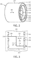
- a RF arrangement 142 which may form part of an embodiment of the invention can be seen in Figs. 2 and 3 .
- the RF arrangement 142 comprises the RF shield 124 and the RF coil 140, which are in this example provided as two individual parts.
- the RF coil 140 comprises a coil PCB 200, multiple conductive rungs 202, which are provided on the coil PCB 200 and extending in an axis of the longitudinal direction 204 of the RF coil 140, a conductive ring 206, provided at each end side of the RF coil 140.
- Conductive rungs 202 and conductive rings 206 serve as conductive elements.
- the RF coil 140 further comprises coupling capacitors 208, which are provided along the conductive rungs 202 and the conductive rings 206.
- the RF coil 140 further comprises multiple feeding ports 210 for the excitation of the conductive elements 202, 206, and a connection port 212.
- the feeding ports 210 are connected to the connection port 212 via feeding lines 214, one of which is shown in Fig. 3 .
- the RF coil 140 of this example is a system integrated body coil with four or eight port feeding.
- the RF coil 140 is integrated in a dedicated head insert gradient coil.
- the head insert gradient coil has preferably an inner diameter of 30 to 40 cm.
- the co-planar feeding line 214 has two axial sections 270 extending in the longitudinal direction 204 of the RF coil 140. Furthermore, the co-planar feeding line 214 has a circumferential section 272 extending in a circumferential direction of the RF coil 140, whereby the circumferential section 272 is provided in a center region with respect to a longitudinal direction 204 of the RF coil 140.
- the conductive rungs 202 and the conductive rings 206 are provided at an inner face 216 of the coil PCB 200.
- the coupling capacitors 208 are provided by capacitive coupling through the coil PCB 200. Accordingly, the coupling capacitors 208 are provided as distributed capacitors.
- the coil PCB 200 comprises an additional metallization on its outer face 218.
- the RF shield 124 comprises a shield PCB 220, which has a patterned metallization on its inner face 222 and on its outer face 224, which form a metallic shield structure 252, as can be seen e.g. with respect to Figs. 7 and 8 .
- the metallizations provide overlapping areas creating distributed capacitors.
- the metallizations are provided as slitted structures, which do not allow low-frequency gradient eddy currents to circulate, but nevertheless to be transparent to RF frequencies of the MR imaging system 110.
- the co-planar feeding line 214 is provided in accordance with the invention as a conductor-backed co-planar waveguide (CBCPW).
- the co-planar feeding line 214 comprises a conducting track 230 having a width W and a pair of return conductors 232, which are provided one to either side of the conducting track 230.
- the conducting track 230 and the return conductors 232 are printed onto one side of a feeding line PCB 234 having a height H.
- the return conductors 232 are separated from the conducting track 230 by a small gap G, which has typically an unvarying width along the length of the feeding line 214.
- the co-planar feeding line 214 further comprises a ground plane 236 covering an area corresponding at least to an area covered by the conducting track 230 and the return conductors 232.
- the ground plane 236 is provided on an opposite face of the feeding line PCB 234.
- the feeding line 214 of the first embodiment is, according to a second embodiment, arranged at the inner face 216 of the coil PCB 200, as can be seen in Fig. 5 .
- the ground plane 236 of the feeding line 214 is provided as a metallization on the coil PCB 200.
- the feeding line PCB 234 is arranged on the ground plane 236, and the conducting track 230 and the return conductors 232 are provided as metallizations on the feeding line PCB 234.
- the coil PCB 200 is provided with a slot 238.
- the feeding line 214 of the first embodiment realized with a co-planar conducting track 230 and return conductors 232 on feeding line PCB234, is arranged entirely within the slot 238 of the coil PCB 200.
- a further example can be seen in Fig. 7 .
- a RF arrangement 142 of this example comprises a RF coil 140 and a RF shield 124, as discussed above.
- the RF shield 124 coaxially encompasses the RF coil 140.
- the RF arrangement 142 of this example is provided as a single part.
- the shield PCB 220 comprises connection lines 246, which are connected e.g. by soldering to a coaxial cable (not shown).
- the coaxial cable serves as connection for the RF coil 140.
- the connection lines 246 are provided as co-planar connection lines 246, and which are arranged at the shield PCB 220, as can be seen e.g. in detail in Fig. 8 .
- the detailed design of the connection lines 246 is as described above with respect to the feeding lines 214 of the different embodiments and examples outside the scope of the invention as defined by the claims.
- a radial connection element 240 is provided, which extends between the shield PCB 220 and the coil PCB 200.
- the connection lines 246 are routed on the shield PCB to a location for connection to the coil PCB 200.
- the radial connection element 240 interconnects the connection lines 246 to the coil PCB 200.
- the radial connection element 240 is provided in a center region of the RF coil 140 with respect to its longitudinal direction 204.
- the connection port 212 of the RF coil 140 is provided in a center area of the RF coil 140 in respect to its longitudinal direction 204.
- the feeding lines 214 extend from the connection port 212 to the feeding ports 210 at both longitudinal ends of the RF coil 140.
- the radial connection element 240 comprises a connection PCB 242 with a connection metallization 244 provided thereon, whereby the connection metallization 244 connects the connection lines 246 of the shield PCB 220 to the coil PCB 200.
- the connection PCB 242 is provided as a flexible PCB.
- the metallization 244 of the radial connection element 240 contacts the connection line 246 of the shield PCB 220 in an area not shown in Fig. 7 .
- the metallization 244 of the radial connection element 240 contacts the connection port 212 of the coil PCB 200 via a coil contact element 250 extending radially through the coil PCB 200.
- the coil contact element 250 can be realized by conductive "vias".
- a still further example can be seen in Fig. 8 .
- a RF arrangement 142 of this example comprises a RF coil 140 and a RF shield 124, as described above with respect to the previous example.
- the RF arrangement 142 of this example differs from the RF arrangement 142 of the previous example merely in respect to the connection of the connection lines 246 to the connection port 212 via the radial connection element 240.
- the design of the radial connection element 240 of this example is identical to that of the radial connection element 240 of the previous example.
- the feeding lines 214 are provided at a radially inner face 216 of the coil PCB 200.
- the coil PCB 200 has a hole 260, and the radial connection element 240 extends through the hole 260 from the shield PCB 220 to the coil PCB 200.
- the connection port 212 of the coil PCB 200 is directly contacted by the metallization 244 of the connection PCB 242 with a soldering connection 262.
- the metallization 244 of the radial connection element 240 directly converts into the connection line 246 of the shield PCB 220.
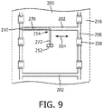
- Fig. 9 is a schematic, planar illustration of a RF coil 140 according to a further example with a co-planar feeding line 214 and a central connection port 212.
- the RF coil 140 corresponds to the RF coil 140 shown in Fig. 3 .
- Hence, only differences between the RF coils 140 will be discussed in detail.
- RF coil 140 of the example shown in Fig. 9 comprises multiple feeding ports 210 for the excitation of the conductive elements 202, 206, and a connection port 212.
- the connection port 212 is arranged in a center region of the RF coil 140.
- the feeding ports 210 are connected to the connection port 212 via feeding lines 214, one of which is shown in Fig. 9 .
- the co-planar feeding line 214 has one axial section 270 extending in the longitudinal direction 204 of the RF coil 140. Furthermore, the co-planar feeding line 214 has a circumferential section 272 extending in a circumferential direction of the RF coil 140, whereby the circumferential section 272 is provided in a center region with respect to a longitudinal direction 204 of the RF coil 140 and connected to the connection port 212.
- the RF shield 124 coaxially encompasses the RF coil 140.
- the RF shield 124 comprises a shield PCB 220, and in a way discussed previously, a connection line 246 is provided on the shield PCB 220. As described above, the connection line 246 is connected via radial connection element 240 to the connection port 212 and the feeding lines 214 of the coil PCB 200.
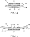
- Fig. 10 shows a shield PCB 220 according to a fourth embodiment.
- a connection line 246 is provided at the shield PCB 220.
- the connection line 246 has in general the same setup as the feeding lines 214.
- the connection line 246 is provided in this embodiment with its ground plane 236 facing away from the shield PCB 220.
- the connection line 246 is provided with its conducting track 230 and its return conductors 232 on the shield PCB 220.
- connection line 246 of the first embodiment is arranged in a slot 238 of the shield PCB 220.
- the co-planar connection line 246 of the fifth embodiment which, according to the invention, is realized with a co-planar conducting track 230 and return conductors 232 on feeding line PCB 234, is arranged entirely within the slot 274 of the shield PCB 220.
Description
- The invention relates to the field of radio frequency (RF) coils for use in a magnetic resonance (MR) imaging system, a RF arrangement for use in a MR imaging system (110), comprising a RF coil and a RF shield, a MR imaging system employing at least one such RF coil, and a MR imaging system employing at least one such RF arrangement.
- In state of the Art MRI-systems, a subject of interest, typically a patient, to be imaged is located somewhere within the free open space near or at the center of a body coil. The body coil can be provided as a birdcage coil with a coil PCB (printed circuit board). The coil PCB has an inner metallization layer, which provides rungs and rings as well as capacitors. The RF coil is typically shielded by a RF shield. The RF shield comprises a shield PCB. The shield PCB has an inner metallization layer with a shielding structure formed therein. The RF shield coaxially encompasses the RF coil. The coil PCB and the shield PCB are non-conductive, and the respective metallization layers are typically made from copper.
- The RF shield and the RF coil can be provided together as a RF arrangement. In the RF arrangement, the RF coils and the RF shield are typically provided as a single component.
- State of the Art RF coils comprise two- or even multi-channel body coils, which use two or more geometrically decoupled feeding ports of a birdcage for RF-shimming. This technique strongly increases the field homogeneity and enables clinical imaging for additional applications at high fields. Most common are two-port RF coils.
- In order to provide power from an external amplifier to the feeding port, the RF coil is typically connected to the amplifier from one side of the RF coil. One feeding port can be directly connected, whereas the other feeding port is connected via a coaxial cable. However, coaxial cables provided on rungs reduce and distort the B1 field. Furthermore, the unilateral feeding may lead to an axially asymmetric distribution of electrical field E and thus increased SAR.
- The axially asymmetric distribution of the electrical field E can at least be partly overcome using four or eight port feeding with fixed phase and amplitude. This feeding requires the routing of several coaxial cables over the whole length of the RF coil, thus potentially increasing local field inhomogeneity. In addition, the feeding lines are incompatible with MRI LINAC.
- The coaxial cables are typically located within the space between the RF coil and the shield. Typically, the coaxial cables are attached to the shield PCB by solder or glue. The coaxial line is made up by an inner conductor, an isolating material, and an outer conductor. By soldering, the outer conductor of the coaxial line gets electric potential identical to the metal on the shield PCB. In principle, the coaxial cables can also be attached to the coil PCB.
- In this context, document
US 2014/0218032 Al refers to a resonator device for spin resonance applications. The resonator device includes a substrate, terminals, and resonators. The terminals include a first terminal having first terminal segments disposed on a substrate surface, and a second terminal having second terminal segments disposed on the substrate surface opposite the first terminal segments. The resonators include conductors disposed on the substrate surface between the first and second terminals. Each conductor is disposed between one of the first terminal segments and a respective, opposite one of the second terminal segments. - Document
US 6,175,237 B1 discloses that two halves of a conventional RF saddle coil, such as spirals or other related structures for use in high resolution NMR or MRI, are disposed on opposite sides of a cylindrical coilform, and rotated from the conventional orientation 90 degrees about the B1 axis, so that the leads are paralleled near the axial center of the RF coil. - Furthermore, document
US 2012/0081119 A1 refers to a probe for an NMR device, in which a saddle coil is disposed on one side of a flexible insulating material, and an additional conductor is disposed on the opposite side. The additional conductor and the conductors of the saddle coil create a capacitance across the insulating material. This capacitance acts with the inductance of the saddle coil such that the probe itself forms a transmission line. The probe is thus inherently broadband and requires no tuning. It also presents a constant impedance, thus facilitating impedance matching to an NMR spectrometer. In a preferred embodiment, a chip resistor is disposed on the flexible insulating material, terminating the transmission line. - Still further, document
WO 2005/052621 A1 refers to a magnetic resonance imaging system including main magnet that produces a substantially spatially and temporally constant main magnetic field within a field of view. Magnetic field gradient coils impose selected magnetic field gradients on the main magnetic field within the field of view. At least one radio frequency coil is arranged to detect a magnetic resonance signal induced by an applied radio frequency pulse. The at least one radio frequency coil includes a radio frequency antenna and electronics module disposed on a substrate. The electronics are electrically connected with the radio frequency antenna. The electronics are mounted in a centered region surrounded by the radio frequency antenna. - Moreover, document
US 2010/0253351 A1 discloses an RF coil assembly for MRI with a microwave antenna feed having an RF trap and a number of microwave transmission lines. - It is an object of the invention to provide a radio frequency (RF) coil for use in a magnetic resonance (MR) imaging system, a RF arrangement for use in a MR imaging system (110), comprising a RF coil and a RF shield, a MR imaging system employing at least one such RF coil, and a MR imaging system employing at least one such RF arrangement, which reduces problems of coaxial cables used in RF coils and RF arrangements. In particular, it is an object of the present invention to enable generation of a B1-field with reduced inhomogeneities and with an increased compatibility for use with MRI LINAC.
- According to the invention, a radio frequency (RF) coil for use in a magnetic resonance (MR) imaging system is provided as defined in claim 1, whereby the RF coil comprises a coil PCB, multiple conductive elements provided on the coil PCB, the multiple conductive elements configured to apply a RF magnetic field to an examination space during RF transmit phases to excite nuclei of a subject of interest, and to receive MR signals from the excited nuclei during RF receive phases, one or multiple feeding ports configured for the excitation of the multiple conductive elements, at least one connection port, and one or multiple feeding lines connecting the at least one connection port to the one or multiple feeding ports, whereby the one or multiple feeding lines are provided as one or more co-planar feeding lines, which are arranged at the coil PCB, whereby each co-planar feeding line is suitable to convey microwave-frequency signals and comprises a conducting track, which is printed onto a dielectric substrate, together with a pair of return conductors, which are provided one to either side of the conducting track, wherein said conducting track and said pair of return conductors are provided co-planar on the same side of the substrate. According to a further aspect, a radio frequency (RF) arrangement for use in a magnetic resonance (MR) imaging system is provided as defined in claim 7.
- According to a further aspect, a magnetic resonance (MR) imaging system is provided as defined in claim 13.
- According to a still further aspect, a magnetic resonance (MR) imaging system is provided as defined in claim 14.
- In other words, the object is solved in the present invention by providing the feeding lines as co-planar feeding lines. This allows having a coil structure of the RF coil and the feeding lines on one single PCB, i.e. no additional coaxial cables need to be added in an extra manual production step. Thus production time and cost of integration are reduced.
- Co-planar feeding lines refer to a type of electrical transmission line, which can be fabricated using printed circuit board technology, and is suitable to convey microwave-frequency signals. Co-planar feeding lines comprise a conducting track, which is printed onto a dielectric substrate, together with a pair of return conductors, which are provided one to either side of the conducting track. All three conductors are on the same side of the substrate, and hence are co-planar. The return conductors are separated from the central track by a small gap, which has an unvarying width along the length of the line.
- Preferably, the RF coil is a system integrated body coil with four or eight port feeding using PCB integrated co-planar RF power feeding lines. The RF coil comprises rings and rungs as conductive elements. Further preferred, feeding port and conductive elements are integrated on one PCB, so that a separate coaxial cable for feeding can be omitted. A coil PCB former can be connected in one process in production without additional routing and soldering of the feeding coax cable, thus saving time and production costs. Coax cables also have a reduced reliability due to the solder process used in the manufacturing process of the RF coil. Furthermore, the integrated feeding design of the RF coil provides better radiation transparency compared with coax feeding for LINAC MRI scanner. Hence, this RF coil architecture is useful for image guided therapy using MRI in combination with proton/LINAC therapy, as no solid coax cable parts are present in the proton/LINAC beam.
- In the RF arrangement, the radial connection element interconnects the connection lines to the coil PCB. However, it is not required that the radial connection element has a strict radial extension between the coil PCB and the shield PCB. Furthermore, the connection lines can be directly or indirectly connected to the connection port. Hence, the at least one radial connection element may be directly connected to the connection port of the RF coil, or via further connection of feeding lines provided on the coil PCB.
- The present and further discussion of the details of the connection lines and the feeding lines are generally applicable to the connection lines and the feeding lines. Furthermore, and more general, the teachings in respect to the RF coil and the RF shield can be applied vice versa. This includes also the radial connection element. According to a preferred embodiment, the co-planar feeding lines are provided as metallization on the coil PCB. With the co-planar feeding lines provided directly on the coil PCB, manufacturing of the RF coil can be facilitated, since no additional PCB is required. Furthermore, the rungs and the feeding lines can be provided in essentially a single production process.
- According to the invention, the co-planar feeding line is provided as conductor-backed co-planar waveguide (CBCPW) with a ground plane covering an area corresponding at least to an area covered by said conducting track and said pair of return conductors of the co-planar feeding line. The conductor-backed co-planar waveguide is a variant of the co-planar waveguide, which has a ground plane covering the entire back-face of the substrate. The ground-plane serves as a third return conductor. Also the conductor-backed co-planar waveguide can be easily manufactured on the coil PCB. However, a separate feeding line PCB is required between the ground plane and the conductors. This has the advantage that a suitable material can be chosen in accordance with requirements of the feeding line. Limitations based on the use of a certain type of PCB, which is e.g. suitable for the RF coil or the RF shield, can be overcome. The conductor-backed co-planar waveguide can be provided on the coil PCB or the shield PCB with its ground plane oriented towards the respective PCB, or vice versa.
- According to a preferred embodiment, the coil PCB is provided with at least one slot, at least one feeding line PCB is provided in the at least one slot, and at least one feeding line is provided on the at least one feeding line PCB. Hence, the feeding line performance can be controlled by free choice of the material of the feeding line PCB without the need to provide the feeding line PCB on top of the coil PCB. Hence, the RF coil can be provided with an essentially uniform outer surface without elevations. The same principles can be applied to the design of the connection lines on the shield PCB.
- According to a preferred embodiment, at least one of the co-planar feeding lines has an axial section extending in a longitudinal direction of the RF coil. Hence, when the connection port is provided laterally at the RF coil, the axial section can extend over essentially the entire length of the RF coil to connect feeding ports at an opposite end of the RF coil. When the RF coil has a central feeding port, axial sections can extend to either end of the RF coil to connect respective feeding ports. The circumferential section typically does not reduce field homogeneity.
- According to a preferred embodiment, at least one of the co-planar feeding lines has a circumferential section extending in a circumferential direction of the RF coil, whereby the circumferential section is provided in a center region with respect to a longitudinal direction of the RF coil. The circumferential section can possibly affect field homogeneity. However, when being provided in the center region, these effects are very small.
- According to a preferred embodiment, at least one of the co-planar feeding lines has an outer section extending on an outer side of the coil PCB, and an inner section extending on an inner side of the coil PCB, whereby the coil PCB is provided with at least a coil contact element extending radially through the coil PCB, which electrically connects the outer section and the inner section. With the coil contact element, a high level of freedom for design of the RF coil is provided, since the feeding lines can be provided as most suitable on either side of the coil PCB.
- According to a preferred embodiment, the at least one radial connection element is provided in a center region of the RF coil with respect to a longitudinal direction of the RF coil. When being provided in the center region, effects of the radial connection element on field homogeneity are typically small.
- According to a preferred embodiment, the at least one radial connection element comprises a connection PCB with a connection metallization provided thereon, whereby the connection metallization connects the multiple connection lines to the coil PCB.
- According to a preferred embodiment, the connection PCB is provided as a flexible PCB. The flexible PCB facilitates design and manufacturing of the RF assembly.
- According to a preferred embodiment, the multiple connection lines are provided at a radially outer face of the shield PCB, the shield PCB has at least one hole, and the at least one radial connection element extends through the at least one hole from the shield PCB to the coil PCB. Hence, either side of the shield PCB can be easily connected using the radial connection element. The hole is preferably provided in a central region of the RF coil or the RF assembly.
- According to a preferred embodiment, the multiple feeding lines are provided at a radially inner face of the coil PCB, the coil PCB has at least one hole, and the at least one radial connection element extends through the at least one hole from the shield PCB to the coil PCB. Hence, either side of the coil PCB can be easily connected using the radial connection element. The hole is preferably provided in a central region of the RF coil or the RF assembly.
- According to a preferred embodiment, at least one of the connection lines has an outer section extending on an outer side of the shield PCB, and an inner section extending on an inner side of the shield PCB, whereby the shield PCB is provided with at least a shield contact element extending radially through the shield PCB, which electrically connects the outer section and the inner section. With the shield contact element, a high level of freedom for design of the RF shield and the RF arrangement is provided, since the connection lines can be provided as most suitable on either side of the shield PCB.
- These and other aspects of the invention will be apparent from and elucidated with reference to the embodiments and examples outside the scope of the invention described hereinafter. Such an embodiment does not necessarily represent the full scope of the invention, however, and reference is made therefore to the claims which define the scope of the invention.
- In the drawings:
-
Fig. 1 is a schematic illustration of a part of a generic magnetic resonance (MR) imaging system which, as such, is outside the scope of the invention as defined by the claims. -
Fig. 2 is a perspective illustration of a radio frequency (RF) arrangement of the magnetic resonance (MR) imaging system ofFig. 1 comprising a RF coil and a RF shield which can be used to perform the present invention. However, the RF arrangement shown inFig. 2 as such is outside the scope of the invention as defined by the claims. -
Fig. 3 is a schematic, planar illustration of a RF coil with a co-planar feeding line which can be used to perform the present invention. However, the RF coil shown inFig. 3 as such is outside the scope of the invention as defined by the claims. -
Fig. 4 is a sectional view of a co-planar feeding line, which is provided as a conductor-backed co-planar waveguide, in accordance with a first embodiment. -
Fig. 5 is a sectional view of the co-planar feeding line ofFig. 4 provided at an inner surface of a coil PCB, in accordance with a second embodiment. -
Fig. 6 is a sectional view of the co-planar feeding line ofFig. 4 provided in the coil PCB, in accordance with a third embodiment. -
Fig. 7 is a sectional view of the coil PCB and the shield PCB, which are connected by a radial connection element, in accordance with an example which, as such, is outside the scope of the invention as defined by the claims. -
Fig. 8 is a sectional view of the coil PCB and the shield PCB, which are connected by a radial connection element extending through a hole in the coil PCB, in accordance with an example which, as such, is outside the scope of the invention as defined by the claims. -
Fig.9 is a schematic, planar illustration of a RF coil with a co-planar feeding line and a central connection port in accordance with an example which, as such, is outside the scope of the invention as defined by the claims. -
Fig. 10 is a sectional view of the co-planar feeding line ofFig. 4 provided at an inner surface of a shield PCB, in accordance with a fourth embodiment, and -
Fig. 11 is a sectional view of the co-planar feeding line ofFig. 4 provided in the shield PCB, in accordance with a fifth embodiment. -
Fig. 1 shows a schematic illustration of a part of a magnetic resonance (MR)imaging system 110 comprising anMR scanner 112. TheMR imaging system 110 is described here generically as a basis for all further embodiments. - The
MR imaging system 110 includes amain magnet 114 provided for generating a static magnetic field. Themain magnet 114 has a central bore that provides anexamination space 116 around acenter axis 118 for a subject ofinterest 120, usually a patient, to be positioned within. In this embodiment, the central bore and therefore the static magnetic field of themain magnet 114 have a horizontal orientation in accordance with thecenter axis 118. In an alternative embodiment, the orientation of themain magnet 114 can be different, e.g. to provide the static magnetic field with a vertical orientation. Further, theMR imaging system 110 comprises a magneticgradient coil system 122 provided for generating gradient magnetic fields superimposed to the static magnetic field. The magneticgradient coil system 122 is concentrically arranged within the bore of themain magnet 114, as known in the art. - Further, the
MR imaging system 110 includes a radio frequency (RF)coil 140 designed as a whole-body coil having a tubular body. In an alternative arrangement, theRF coil 140 is designed as a head coil or any other suitable coil type for use inMR imaging systems 110. TheRF coil 140 is provided for applying a RF magnetic field to theexamination space 116 during RF transmit phases to excite nuclei of the subject ofinterest 120, which shall be covered by MR images. TheRF coil 140 is also provided to receive MR signals from the excited nuclei during RF receive phases. In a state of operation of theMR imaging system 110, RF transmit phases and RF receive phases are taking place in a consecutive manner. TheRF coil 140 is arranged concentrically within the bore of themain magnet 114. As is known in the art, acylindrical RF shield 124 is arranged concentrically between the magneticgradient coil system 122 and theRF coil 140. Hence, theRF shield 124 coaxially encompasses theRF coil 140. In some examples, theRF coil 140 and theRF shield 124 are provided integrally, thereby forming a radio frequency (RF)arrangement 142. - Moreover, the
MR imaging system 110 comprises an MRimage reconstruction unit 130 provided for reconstructing MR images from the acquired MR signals and an MR imagingsystem control unit 126 with amonitor unit 128 provided to control functions of theMR scanner 112, as is commonly known in the art.Control lines 138 are installed between the MR imagingsystem control unit 126 and aRF transmitter unit 134 that is provided to feed RF power of an MR radio frequency to theRF coil 140 via aRF switching unit 136 during the RF transmit phases. TheRF switching unit 136 in turn is also controlled by the MR imagingsystem control unit 126, and anothercontrol line 132 is installed between the MR imagingsystem control unit 126 and theRF switching unit 136 to serve that purpose. During RF receive phase, theRF switching unit 136 directs the MR signals from theRF coil 140 to the MRimage reconstruction unit 130 after pre-amplification. - A
RF arrangement 142 which may form part of an embodiment of the invention can be seen inFigs. 2 and 3 . TheRF arrangement 142 comprises theRF shield 124 and theRF coil 140, which are in this example provided as two individual parts. - As can be seen in detail with respect to
Fig. 2 , theRF coil 140 comprises acoil PCB 200, multipleconductive rungs 202, which are provided on thecoil PCB 200 and extending in an axis of thelongitudinal direction 204 of theRF coil 140, aconductive ring 206, provided at each end side of theRF coil 140.Conductive rungs 202 andconductive rings 206 serve as conductive elements. TheRF coil 140 further comprisescoupling capacitors 208, which are provided along theconductive rungs 202 and the conductive rings 206. As can be seen under additional consideration ofFig. 3 , theRF coil 140 further comprises multiple feedingports 210 for the excitation of theconductive elements connection port 212. The feedingports 210 are connected to theconnection port 212 via feedinglines 214, one of which is shown inFig. 3 . TheRF coil 140 of this example is a system integrated body coil with four or eight port feeding. In an alternative example, theRF coil 140 is integrated in a dedicated head insert gradient coil. The head insert gradient coil has preferably an inner diameter of 30 to 40 cm. - As can be further seen in
Fig. 3 , theco-planar feeding line 214 has twoaxial sections 270 extending in thelongitudinal direction 204 of theRF coil 140. Furthermore, theco-planar feeding line 214 has acircumferential section 272 extending in a circumferential direction of theRF coil 140, whereby thecircumferential section 272 is provided in a center region with respect to alongitudinal direction 204 of theRF coil 140. - According to the example, the
conductive rungs 202 and theconductive rings 206 are provided at aninner face 216 of thecoil PCB 200. In an alternative example, thecoupling capacitors 208 are provided by capacitive coupling through thecoil PCB 200. Accordingly, thecoupling capacitors 208 are provided as distributed capacitors. In this alternative example, thecoil PCB 200 comprises an additional metallization on itsouter face 218. - The
RF shield 124 comprises ashield PCB 220, which has a patterned metallization on itsinner face 222 and on itsouter face 224, which form ametallic shield structure 252, as can be seen e.g. with respect toFigs. 7 and 8 . The metallizations provide overlapping areas creating distributed capacitors. The metallizations are provided as slitted structures, which do not allow low-frequency gradient eddy currents to circulate, but nevertheless to be transparent to RF frequencies of theMR imaging system 110. - One of the
co-planar feeding lines 214 of theRF coil 140 is shown separately inFig. 4 with respect to a first embodiment. Theco-planar feeding line 214 is provided in accordance with the invention as a conductor-backed co-planar waveguide (CBCPW). Theco-planar feeding line 214 comprises a conductingtrack 230 having a width W and a pair ofreturn conductors 232, which are provided one to either side of the conductingtrack 230. The conductingtrack 230 and thereturn conductors 232 are printed onto one side of afeeding line PCB 234 having a height H. Thereturn conductors 232 are separated from the conductingtrack 230 by a small gap G, which has typically an unvarying width along the length of thefeeding line 214. - The
co-planar feeding line 214 further comprises aground plane 236 covering an area corresponding at least to an area covered by the conductingtrack 230 and thereturn conductors 232. Theground plane 236 is provided on an opposite face of thefeeding line PCB 234. - The
feeding line 214 of the first embodiment is, according to a second embodiment, arranged at theinner face 216 of thecoil PCB 200, as can be seen inFig. 5 . Hence, theground plane 236 of thefeeding line 214 is provided as a metallization on thecoil PCB 200. Thefeeding line PCB 234 is arranged on theground plane 236, and the conductingtrack 230 and thereturn conductors 232 are provided as metallizations on thefeeding line PCB 234. - According to a third embodiment, which can be seen in
Fig. 6 , thecoil PCB 200 is provided with aslot 238. Thefeeding line 214 of the first embodiment, realized with aco-planar conducting track 230 and returnconductors 232 on feeding line PCB234, is arranged entirely within theslot 238 of thecoil PCB 200. - A further example can be seen in
Fig. 7 . ARF arrangement 142 of this example comprises aRF coil 140 and aRF shield 124, as discussed above. TheRF shield 124 coaxially encompasses theRF coil 140. TheRF arrangement 142 of this example is provided as a single part. - In this example, the
shield PCB 220 comprisesconnection lines 246, which are connected e.g. by soldering to a coaxial cable (not shown). The coaxial cable serves as connection for theRF coil 140. The connection lines 246 are provided asco-planar connection lines 246, and which are arranged at theshield PCB 220, as can be seen e.g. in detail inFig. 8 . The detailed design of the connection lines 246 is as described above with respect to thefeeding lines 214 of the different embodiments and examples outside the scope of the invention as defined by the claims. - Furthermore, as can be seen in
Fig. 7 , aradial connection element 240 is provided, which extends between theshield PCB 220 and thecoil PCB 200. The connection lines 246 are routed on the shield PCB to a location for connection to thecoil PCB 200. Theradial connection element 240 interconnects theconnection lines 246 to thecoil PCB 200. Theradial connection element 240 is provided in a center region of theRF coil 140 with respect to itslongitudinal direction 204. Hence, theconnection port 212 of theRF coil 140 is provided in a center area of theRF coil 140 in respect to itslongitudinal direction 204. The feeding lines 214 extend from theconnection port 212 to the feedingports 210 at both longitudinal ends of theRF coil 140. - The
radial connection element 240 comprises aconnection PCB 242 with aconnection metallization 244 provided thereon, whereby theconnection metallization 244 connects theconnection lines 246 of theshield PCB 220 to thecoil PCB 200. Theconnection PCB 242 is provided as a flexible PCB. - According to a further example, the
metallization 244 of theradial connection element 240 contacts theconnection line 246 of theshield PCB 220 in an area not shown inFig. 7 . Themetallization 244 of theradial connection element 240 contacts theconnection port 212 of thecoil PCB 200 via acoil contact element 250 extending radially through thecoil PCB 200. Thecoil contact element 250 can be realized by conductive "vias". - A still further example can be seen in
Fig. 8 . ARF arrangement 142 of this example comprises aRF coil 140 and aRF shield 124, as described above with respect to the previous example. - The
RF arrangement 142 of this example differs from theRF arrangement 142 of the previous example merely in respect to the connection of theconnection lines 246 to theconnection port 212 via theradial connection element 240. However, the design of theradial connection element 240 of this example is identical to that of theradial connection element 240 of the previous example. - According to this example, the
feeding lines 214 are provided at a radiallyinner face 216 of thecoil PCB 200. Furthermore, thecoil PCB 200 has ahole 260, and theradial connection element 240 extends through thehole 260 from theshield PCB 220 to thecoil PCB 200. Hence, theconnection port 212 of thecoil PCB 200 is directly contacted by themetallization 244 of theconnection PCB 242 with asoldering connection 262. - In this example, the
metallization 244 of theradial connection element 240 directly converts into theconnection line 246 of theshield PCB 220. -
Fig. 9 is a schematic, planar illustration of aRF coil 140 according to a further example with aco-planar feeding line 214 and acentral connection port 212. As can be seen in detail inFig. 9 , theRF coil 140 corresponds to theRF coil 140 shown inFig. 3 . Hence, only differences between the RF coils 140 will be discussed in detail. -
RF coil 140 of the example shown inFig. 9 comprises multiple feedingports 210 for the excitation of theconductive elements connection port 212. Theconnection port 212 is arranged in a center region of theRF coil 140. The feedingports 210 are connected to theconnection port 212 via feedinglines 214, one of which is shown inFig. 9 . - As can be further seen in
Fig. 9 , theco-planar feeding line 214 has oneaxial section 270 extending in thelongitudinal direction 204 of theRF coil 140. Furthermore, theco-planar feeding line 214 has acircumferential section 272 extending in a circumferential direction of theRF coil 140, whereby thecircumferential section 272 is provided in a center region with respect to alongitudinal direction 204 of theRF coil 140 and connected to theconnection port 212. - Also in this further example, the
RF shield 124 coaxially encompasses theRF coil 140. TheRF shield 124 comprises ashield PCB 220, and in a way discussed previously, aconnection line 246 is provided on theshield PCB 220. As described above, theconnection line 246 is connected viaradial connection element 240 to theconnection port 212 and thefeeding lines 214 of thecoil PCB 200. -
Fig. 10 shows ashield PCB 220 according to a fourth embodiment. Accordingly aconnection line 246 is provided at theshield PCB 220. As can be seen inFig. 10 , theconnection line 246 has in general the same setup as the feeding lines 214. However, according to the fourth embodiment, theconnection line 246 is provided in this embodiment with itsground plane 236 facing away from theshield PCB 220. According to the fourth embodiment, theconnection line 246 is provided with its conductingtrack 230 and itsreturn conductors 232 on theshield PCB 220. - According to a fifth embodiment, the
connection line 246 of the first embodiment is arranged in aslot 238 of theshield PCB 220. Theco-planar connection line 246 of the fifth embodiment which, according to the invention, is realized with aco-planar conducting track 230 and returnconductors 232 on feedingline PCB 234, is arranged entirely within theslot 274 of theshield PCB 220. - While the invention has been illustrated and described in detail in the drawings and foregoing description, such illustration and description are to be considered illustrative or exemplary and not restrictive; the invention is defined by the claims and is not limited to the disclosed embodiments. Other variations to the disclosed embodiments can be understood and effected by those skilled in the art in practicing the claimed invention, from a study of the drawings, the disclosure, and the appended claims. In the claims, the word "comprising" does not exclude other elements or steps, and the indefinite article "a" or "an" does not exclude a plurality. The mere fact that certain measures are recited in mutually different dependent claims does not indicate that a combination of these measures cannot be used to advantage, provided that said combination falls within the scope of the invention as defined by the claims.
- Any reference signs in the claims should not be construed as limiting the scope.
-
- 110
- magnetic resonance (MR) imaging system
- 112
- magnetic resonance (MR) scanner
- 114
- main magnet
- 116
- RF examination space
- 118
- center axis
- 120
- subject of interest
- 122
- magnetic gradient coil system
- 124
- radio frequency (RF) shield
- 126
- MR imaging system control unit
- 128
- monitor unit
- 130
- MR image reconstruction unit
- 132
- control line
- 134
- RF transmitter unit
- 136
- RF switching unit
- 138
- control line
- 140
- radio frequency (RF) coil
- 142
- radio frequency (RF) arrangement
- 200
- coil PCB
- 202
- conductive rung, conductive element
- 204
- longitudinal direction
- 206
- conductive ring
- 208
- coupling capacitors
- 210
- feeding port
- 212
- connection port
- 214
- feeding line
- 216
- inner face/metallisation (coil PCB)
- 218
- outer face/metallisation (coil PCB)
- 220
- shield PCB
- 222
- inner face/metallisation (shield PCB)
- 224
- outer face/metallisation (shield PCB)
- 230
- conducting track, conductor
- 232
- return conductor, conductor
- 234
- feeding line PCB
- 236
- ground plane
- 238
- slot (coil PCB)
- 240
- radial connection element
- 242
- connection PCB
- 244
- metallization (connection PCB)
- 246
- connection line
- 250
- coil contact element
- 252
- metallic shield structure
- 260
- hole
- 262
- soldering connection
- 270
- axial section
- 272
- circumferential section
- 274
- slot (shield PCB)
- W
- width (conducting track)
- H
- height (feeding line PCB)
- G
- gap
Claims (14)
- A radio frequency (RF) coil (140) for use in a magnetic resonance (MR) imaging system (110), whereby the RF coil (140) comprises a coil printed circuit board (PCB) (200),multiple conductive elements (202, 206) provided on the coil PCB (200), the multiple conductive elements configured to apply a RF magnetic field to an examination space (116) during RF transmit phases to excite nuclei of a subject of interest (120), and to receive MR signals from the excited nuclei during RF receive phases,one or multiple feeding ports (210) configured for the excitation of the multiple conductive elements (202),at least one connection port (212), andone or multiple feeding lines (214) connecting the at least one connection port (212) to the one or multiple feeding ports (210), wherebythe one or multiple feeding lines (214) are provided as one or more co-planar feeding lines, which are arranged at the coil PCB (200), wherebyeach co-planar feeding line (214) is suitable to convey microwave-frequency signals and comprises a conducting track (230), which is printed onto a dielectric substrate (234), together with a pair of return conductors (232), which are provided one to either side of the conducting track (230), wherein said conducting track (230) and said pair of return conductors (232) are provided co-planar on the same side of the substrate (234), wherein the co-planar feeding line (214) is provided as conductor-backed co-planar waveguide (CBCPW) with a ground plane (236) covering an area corresponding at least to an area covered by said conducting track and said pair of return conductors (230, 232) of the co-planar feeding line (214).
- The radio frequency (RF) coil (140) according to preceding claim 1, wherein
the co-planar feeding lines (214) are provided as metallization on the coil PCB (200). - The radio frequency (RF) coil (140) according to any preceding claim, whereinthe coil PCB (200) is provided with at least one slot (238),at least one feeding line PCB (234) is provided in the at least one slot (238), andat least one feeding line (214) is provided on the at least one feeding line PCB (234).
- The radio frequency (RF) coil (140) according to any preceding claim, wherein
at least one of the co-planar feeding lines (214) has an axial section (270) extending in a longitudinal direction (204) of the RF coil (140). - The radio frequency (RF) coil (140) according to any preceding claim, wherein
at least one of the co-planar feeding lines (214) has a circumferential section (272) extending in a circumferential direction of the RF coil (200), whereby the circumferential section (272) is provided in a center region with respect to a longitudinal direction (204) of the RF coil (140). - The radio frequency (RF) coil (140) according to any preceding claim, whereinat least one of the co-planar feeding lines (214) has an outer section extending on an outer side (218) of the coil PCB (200), and an inner section extending on an inner side (216) of the coil PCB (200),whereby the coil PCB (200) is provided with at least a coil contact element (250) extending radially through the coil PCB (200), which electrically connects the outer section and the inner section.
- A radio frequency (RF) arrangement (142) for use in a magnetic resonance (MR) imaging system (110), comprising a RF coil (140) according to any preceding claim and a RF shield (124), whereby the RF shield (124) coaxially encompasses the RF coil (140), the RF shield (124) comprisinga shield PCB (220),a metallic shield structure (252) provided at the shield PCB (220), and multiple connection lines (246) connected to the at least one connection port (212), whereby the multiple connection lines (246) are provided as co-planar connection lines, which are arranged at the shield PCB (220), andat least one radial connection element (240), which extends between the shield PCB (220) and the coil PCB (200), and which electrically connects the multiple connection lines (246) to the coil PCB (200) for connection to the at least one connection port (212).
- The radio frequency (RF) arrangement (142) according to preceding claim 7, wherein
the at least one radial connection element (240) is provided in a center region of the RF coil (200) with respect to a longitudinal direction (204) of the RF coil (140). - The radio frequency (RF) arrangement (142) according to any of preceding claims 7 or 8, wherein
the at least one radial connection element (240) comprises a connection PCB (242) with a connection metallization (244) provided thereon, whereby the connection metallization (244) connects the multiple connection lines (246) to the at least one connection port (212) of the coil PCB (200). - The radio frequency (RF) arrangement (142) according to any of preceding claims 7 to 9, whereinthe multiple connection lines (246) are provided at a radially outer face (224) of the shield PCB (220),the shield PCB (220) has at least one hole (260), andthe at least one radial connection element (240) extends through the at least one hole (260) from the shield PCB (220) to the coil PCB (200).
- The radio frequency (RF) arrangement (142) according to any of preceding claims 7 to 10, whereinthe multiple feeding lines (214) are provided at a radially inner face (216) of the coil PCB (200),the coil PCB (200) has at least one hole (260), andthe at least one radial connection element (240) extends through the at least one hole (260) from the shield PCB (220) to the coil PCB (200).
- The radio frequency (RF) arrangement (142) according to any of preceding claims 7 to 11, whereinat least one of the connection lines (246) has an outer section extending on an outer side (224) of the shield PCB (220), and an inner section extending on an inner side (222) of the shield PCB (220), wherebythe shield PCB (220) is provided with at least a shield contact element extending radially through the shield PCB (220), which electrically connects the outer section and the inner section.
- A magnetic resonance (MR) imaging system (110), comprisinga tubular examination space (116) provided to position a subject of interest (120) therein,at least one radio frequency (RF) coil (140) according to any of claims 1 to 6,a RF screen (124) for shielding the examination space (116),a magnetic gradient coil system (122) for generating gradient magnetic fields superimposed to the static magnetic field, anda main magnet (114) for generating a static magnetic field,whereby the RF coil (140), the RF screen (124), the magnetic gradient coil system (122) and the main magnet (114) are positioned in this order in a direction radially outward around the examination space (116).
- A magnetic resonance (MR) imaging system (110), comprisinga tubular examination space (116) provided to position a subject of interest (120) therein,a magnetic gradient coil system (122) for generating gradient magnetic fields superimposed to the static magnetic field,a main magnet (114) for generating a static magnetic field, andat least one radio frequency (RF) arrangement (142) according to any of claims 7 to 12,whereby the RF arrangement (142), the magnetic gradient coil system (122), and the main magnet (114) are positioned in this order in a direction radially outward around the examination space (116).
Applications Claiming Priority (3)
| Application Number | Priority Date | Filing Date | Title |
|---|---|---|---|
| EP16193034 | 2016-10-10 | ||
| EP16200907 | 2016-11-28 | ||
| PCT/EP2017/075672 WO2018069247A1 (en) | 2016-10-10 | 2017-10-09 | Co-planar rf coil feeding |
Publications (2)
| Publication Number | Publication Date |
|---|---|
| EP3523666A1 EP3523666A1 (en) | 2019-08-14 |
| EP3523666B1 true EP3523666B1 (en) | 2022-04-27 |
Family
ID=60001935
Family Applications (1)
| Application Number | Title | Priority Date | Filing Date |
|---|---|---|---|
| EP17777936.0A Active EP3523666B1 (en) | 2016-10-10 | 2017-10-09 | Co-planar rf coil feeding |
Country Status (7)
| Country | Link |
|---|---|
| US (1) | US10877114B2 (en) |
| EP (1) | EP3523666B1 (en) |
| JP (1) | JP7036809B6 (en) |
| CN (1) | CN109804260B (en) |
| BR (1) | BR112019006953A2 (en) |
| RU (1) | RU2744714C2 (en) |
| WO (1) | WO2018069247A1 (en) |
Families Citing this family (4)
| Publication number | Priority date | Publication date | Assignee | Title |
|---|---|---|---|---|
| EP3761051A1 (en) | 2019-07-04 | 2021-01-06 | Siemens Healthcare GmbH | Local coil with segmented antenna device |
| CA3156997A1 (en) * | 2019-10-08 | 2021-04-15 | Hyperfine Operations, Inc. | System and methods for detecting electromagnetic interference in patients during magnetic resonance imaging |
| KR102644728B1 (en) * | 2021-03-25 | 2024-03-11 | 가천대학교 산학협력단 | Inductively coupled micro-stripline RF coil for MRI |
| US20220349965A1 (en) * | 2021-04-28 | 2022-11-03 | Shanghai United Imaging Healthcare Co., Ltd. | Coil assembly and magnetic resonance system |
Family Cites Families (24)
| Publication number | Priority date | Publication date | Assignee | Title |
|---|---|---|---|---|
| CN2221939Y (en) * | 1995-06-05 | 1996-03-13 | 深圳安科高技术有限公司 | Radio-frequency coil device for magnetic resonance imaging system |
| US6175237B1 (en) | 1997-03-05 | 2001-01-16 | Doty Scientific, Inc. | Center-fed paralleled coils for MRI |
| US6535084B1 (en) * | 2000-01-15 | 2003-03-18 | Ge Medical Systems Global Technology Company, Llc | Method and apparatus for designing an RF coil assembly |
| WO2003058283A1 (en) | 2001-12-31 | 2003-07-17 | The Johns Hopkins University School Of Medicine | Mri tunable antenna and system |
| CN1714300A (en) * | 2002-11-20 | 2005-12-28 | 皇家飞利浦电子股份有限公司 | Self-shielded gradient field coil for magnetic resonance imaging |
| EP1480250A1 (en) * | 2003-05-22 | 2004-11-24 | HELYSSEN S.à.r.l. | A high density plasma reactor and RF-antenna therefor |
| JP2007512071A (en) * | 2003-11-25 | 2007-05-17 | コーニンクレッカ フィリップス エレクトロニクス エヌ ヴィ | Magnetic resonance coil element with built-in electronic module |
| EP1709458A1 (en) * | 2004-01-15 | 2006-10-11 | Koninklijke Philips Electronics N.V. | Planar rf resonator for open mri systems |
| EP1761791A2 (en) * | 2004-06-25 | 2007-03-14 | Koninklijke Philips Electronics N.V. | Integrated power supply for surface coils |
| US7755357B2 (en) | 2004-12-22 | 2010-07-13 | Koninklijke Philips Electronics N.V. | Radio frequency coil with transmission line end-rings |
| WO2008075309A1 (en) | 2006-12-21 | 2008-06-26 | Koninklijke Philips Electronics N.V. | Power supply for rf coils |
| US8164336B1 (en) | 2007-11-10 | 2012-04-24 | Murphree Jr Dennis Haaga | Transmission line probe for NMR |
| US8035384B2 (en) * | 2008-10-23 | 2011-10-11 | General Electric Company | Hybrid birdcage-TEM radio frequency (RF) coil for multinuclear MRI/MRS |
| GB0820689D0 (en) | 2008-11-12 | 2008-12-17 | Siemens Ag | Antenna arrangement |
| GB0905769D0 (en) | 2009-04-03 | 2009-05-20 | Siemens Ag | Microwave connection |
| US8754819B2 (en) * | 2010-03-12 | 2014-06-17 | Agc Automotive Americas R&D, Inc. | Antenna system including a circularly polarized antenna |
| JP5865353B2 (en) * | 2010-05-27 | 2016-02-17 | コーニンクレッカ フィリップス エヌ ヴェKoninklijke Philips N.V. | Decoupling of multiple channels of MRIRF coil array |
| DE102010027295B4 (en) | 2010-07-16 | 2013-07-25 | Siemens Aktiengesellschaft | Drum standing wave trap |
| JPWO2012165295A1 (en) | 2011-05-31 | 2015-02-23 | 国立大学法人大阪大学 | Resonant circuit |
| EP2745132B1 (en) * | 2011-10-18 | 2020-12-09 | Koninklijke Philips N.V. | Mri coil assembly with a radio frequency shield switchable between a blocking state and a transparent state |
| US9261574B2 (en) | 2012-05-02 | 2016-02-16 | General Electric Company | Structured RF coil assembly for MRI scanner |
| US8482362B1 (en) | 2012-08-15 | 2013-07-09 | Werlatone, Inc. | Combiner/divider with interconnection structure |
| US9841484B2 (en) * | 2013-02-01 | 2017-12-12 | Quantum Valley Investment Fund LP | Resonator device for electron spin resonance |
| US10185000B2 (en) | 2014-10-16 | 2019-01-22 | Koninklikje Philips N.V. | MRI birdcage coil with distributed excitation |
-
2017
- 2017-10-09 JP JP2019518103A patent/JP7036809B6/en active Active
- 2017-10-09 RU RU2019113759A patent/RU2744714C2/en active
- 2017-10-09 EP EP17777936.0A patent/EP3523666B1/en active Active
- 2017-10-09 CN CN201780062401.1A patent/CN109804260B/en active Active
- 2017-10-09 US US16/340,396 patent/US10877114B2/en active Active
- 2017-10-09 BR BR112019006953A patent/BR112019006953A2/en active Search and Examination
- 2017-10-09 WO PCT/EP2017/075672 patent/WO2018069247A1/en active Application Filing
Also Published As
| Publication number | Publication date |
|---|---|
| US20190227133A1 (en) | 2019-07-25 |
| RU2744714C2 (en) | 2021-03-15 |
| EP3523666A1 (en) | 2019-08-14 |
| JP2019532725A (en) | 2019-11-14 |
| BR112019006953A2 (en) | 2019-07-02 |
| CN109804260A (en) | 2019-05-24 |
| US10877114B2 (en) | 2020-12-29 |
| JP7036809B2 (en) | 2022-03-15 |
| WO2018069247A1 (en) | 2018-04-19 |
| RU2019113759A3 (en) | 2021-01-15 |
| RU2019113759A (en) | 2020-11-13 |
| CN109804260B (en) | 2021-09-28 |
| JP7036809B6 (en) | 2022-05-30 |
Similar Documents
| Publication | Publication Date | Title |
|---|---|---|
| EP3523666B1 (en) | Co-planar rf coil feeding | |
| US7755357B2 (en) | Radio frequency coil with transmission line end-rings | |
| US7538552B2 (en) | Orthogonal coil for magnetic resonance imaging | |
| US20070229076A1 (en) | Coil apparatus and nuclear magnetic resonance apparatus using the same | |
| EP3559690B1 (en) | Rf coil device and rf shield device for different mri modes | |
| US9581665B2 (en) | Systems and methods for damping common-mode energy | |
| US8912797B2 (en) | Printed circuit board with integrated shielding | |
| JP2019532725A5 (en) | ||
| KR101846351B1 (en) | Magnetic resonance device | |
| US7068035B2 (en) | Magnetic resonance apparatus with a detunable RF resonator | |
| US7015695B2 (en) | Shielded TEM surface array for parallel imaging | |
| US20220206091A1 (en) | A coil assembly for mr imaging applications | |
| US10942235B2 (en) | Microstrip transmission line array RF coil, RF shield configuration and integrated apparatus of RF coil and radiation imaging device | |
| US6781379B2 (en) | Cable routing and potential equalizing ring for magnetic resonance imaging coils | |
| US7173422B2 (en) | Generator for generating time-variable magnetic fields and magnetic resonance device | |
| EP3855198A1 (en) | A coil assembly for mr imaging applications | |
| CN117120864A (en) | Cable bundle with multiple RF chokes and magnetic resonance system | |
| CN112180309A (en) | Local coil with segmented antenna arrangement | |
| CN113504494A (en) | Four-end ring birdcage radio frequency coil system supporting three-nuclide imaging |
Legal Events
| Date | Code | Title | Description |
|---|---|---|---|
| STAA | Information on the status of an ep patent application or granted ep patent |
Free format text: STATUS: UNKNOWN |
|
| STAA | Information on the status of an ep patent application or granted ep patent |
Free format text: STATUS: THE INTERNATIONAL PUBLICATION HAS BEEN MADE |
|
| PUAI | Public reference made under article 153(3) epc to a published international application that has entered the european phase |
Free format text: ORIGINAL CODE: 0009012 |
|
| STAA | Information on the status of an ep patent application or granted ep patent |
Free format text: STATUS: REQUEST FOR EXAMINATION WAS MADE |
|
| 17P | Request for examination filed |
Effective date: 20190510 |
|
| AK | Designated contracting states |
Kind code of ref document: A1 Designated state(s): AL AT BE BG CH CY CZ DE DK EE ES FI FR GB GR HR HU IE IS IT LI LT LU LV MC MK MT NL NO PL PT RO RS SE SI SK SM TR |
|
| AX | Request for extension of the european patent |
Extension state: BA ME |
|
| DAV | Request for validation of the european patent (deleted) | ||
| DAX | Request for extension of the european patent (deleted) | ||
| RAP1 | Party data changed (applicant data changed or rights of an application transferred) |
Owner name: KONINKLIJKE PHILIPS N.V. |
|
| GRAP | Despatch of communication of intention to grant a patent |
Free format text: ORIGINAL CODE: EPIDOSNIGR1 |
|
| STAA | Information on the status of an ep patent application or granted ep patent |
Free format text: STATUS: GRANT OF PATENT IS INTENDED |
|
| INTG | Intention to grant announced |
Effective date: 20211202 |
|
| GRAS | Grant fee paid |
Free format text: ORIGINAL CODE: EPIDOSNIGR3 |
|
| GRAA | (expected) grant |
Free format text: ORIGINAL CODE: 0009210 |
|
| STAA | Information on the status of an ep patent application or granted ep patent |
Free format text: STATUS: THE PATENT HAS BEEN GRANTED |
|
| AK | Designated contracting states |
Kind code of ref document: B1 Designated state(s): AL AT BE BG CH CY CZ DE DK EE ES FI FR GB GR HR HU IE IS IT LI LT LU LV MC MK MT NL NO PL PT RO RS SE SI SK SM TR |
|
| REG | Reference to a national code |
Ref country code: GB Ref legal event code: FG4D |
|
| REG | Reference to a national code |
Ref country code: CH Ref legal event code: EP |
|
| REG | Reference to a national code |
Ref country code: AT Ref legal event code: REF Ref document number: 1487344 Country of ref document: AT Kind code of ref document: T Effective date: 20220515 |
|
| REG | Reference to a national code |
Ref country code: DE Ref legal event code: R096 Ref document number: 602017056590 Country of ref document: DE |
|
| REG | Reference to a national code |
Ref country code: IE Ref legal event code: FG4D |
|
| REG | Reference to a national code |
Ref country code: DE Ref legal event code: R084 Ref document number: 602017056590 Country of ref document: DE |
|
| REG | Reference to a national code |
Ref country code: GB Ref legal event code: 746 Effective date: 20220624 |
|
| REG | Reference to a national code |
Ref country code: LT Ref legal event code: MG9D |
|
| REG | Reference to a national code |
Ref country code: NL Ref legal event code: MP Effective date: 20220427 |
|
| REG | Reference to a national code |
Ref country code: AT Ref legal event code: MK05 Ref document number: 1487344 Country of ref document: AT Kind code of ref document: T Effective date: 20220427 |
|
| PG25 | Lapsed in a contracting state [announced via postgrant information from national office to epo] |
Ref country code: NL Free format text: LAPSE BECAUSE OF FAILURE TO SUBMIT A TRANSLATION OF THE DESCRIPTION OR TO PAY THE FEE WITHIN THE PRESCRIBED TIME-LIMIT Effective date: 20220427 |
|
| PG25 | Lapsed in a contracting state [announced via postgrant information from national office to epo] |
Ref country code: SE Free format text: LAPSE BECAUSE OF FAILURE TO SUBMIT A TRANSLATION OF THE DESCRIPTION OR TO PAY THE FEE WITHIN THE PRESCRIBED TIME-LIMIT Effective date: 20220427 Ref country code: PT Free format text: LAPSE BECAUSE OF FAILURE TO SUBMIT A TRANSLATION OF THE DESCRIPTION OR TO PAY THE FEE WITHIN THE PRESCRIBED TIME-LIMIT Effective date: 20220829 Ref country code: NO Free format text: LAPSE BECAUSE OF FAILURE TO SUBMIT A TRANSLATION OF THE DESCRIPTION OR TO PAY THE FEE WITHIN THE PRESCRIBED TIME-LIMIT Effective date: 20220727 Ref country code: LT Free format text: LAPSE BECAUSE OF FAILURE TO SUBMIT A TRANSLATION OF THE DESCRIPTION OR TO PAY THE FEE WITHIN THE PRESCRIBED TIME-LIMIT Effective date: 20220427 Ref country code: HR Free format text: LAPSE BECAUSE OF FAILURE TO SUBMIT A TRANSLATION OF THE DESCRIPTION OR TO PAY THE FEE WITHIN THE PRESCRIBED TIME-LIMIT Effective date: 20220427 Ref country code: GR Free format text: LAPSE BECAUSE OF FAILURE TO SUBMIT A TRANSLATION OF THE DESCRIPTION OR TO PAY THE FEE WITHIN THE PRESCRIBED TIME-LIMIT Effective date: 20220728 Ref country code: FI Free format text: LAPSE BECAUSE OF FAILURE TO SUBMIT A TRANSLATION OF THE DESCRIPTION OR TO PAY THE FEE WITHIN THE PRESCRIBED TIME-LIMIT Effective date: 20220427 Ref country code: ES Free format text: LAPSE BECAUSE OF FAILURE TO SUBMIT A TRANSLATION OF THE DESCRIPTION OR TO PAY THE FEE WITHIN THE PRESCRIBED TIME-LIMIT Effective date: 20220427 Ref country code: BG Free format text: LAPSE BECAUSE OF FAILURE TO SUBMIT A TRANSLATION OF THE DESCRIPTION OR TO PAY THE FEE WITHIN THE PRESCRIBED TIME-LIMIT Effective date: 20220727 Ref country code: AT Free format text: LAPSE BECAUSE OF FAILURE TO SUBMIT A TRANSLATION OF THE DESCRIPTION OR TO PAY THE FEE WITHIN THE PRESCRIBED TIME-LIMIT Effective date: 20220427 |
|
| PG25 | Lapsed in a contracting state [announced via postgrant information from national office to epo] |
Ref country code: RS Free format text: LAPSE BECAUSE OF FAILURE TO SUBMIT A TRANSLATION OF THE DESCRIPTION OR TO PAY THE FEE WITHIN THE PRESCRIBED TIME-LIMIT Effective date: 20220427 Ref country code: PL Free format text: LAPSE BECAUSE OF FAILURE TO SUBMIT A TRANSLATION OF THE DESCRIPTION OR TO PAY THE FEE WITHIN THE PRESCRIBED TIME-LIMIT Effective date: 20220427 Ref country code: LV Free format text: LAPSE BECAUSE OF FAILURE TO SUBMIT A TRANSLATION OF THE DESCRIPTION OR TO PAY THE FEE WITHIN THE PRESCRIBED TIME-LIMIT Effective date: 20220427 Ref country code: IS Free format text: LAPSE BECAUSE OF FAILURE TO SUBMIT A TRANSLATION OF THE DESCRIPTION OR TO PAY THE FEE WITHIN THE PRESCRIBED TIME-LIMIT Effective date: 20220827 |
|
| REG | Reference to a national code |
Ref country code: DE Ref legal event code: R097 Ref document number: 602017056590 Country of ref document: DE |
|
| PG25 | Lapsed in a contracting state [announced via postgrant information from national office to epo] |
Ref country code: SM Free format text: LAPSE BECAUSE OF FAILURE TO SUBMIT A TRANSLATION OF THE DESCRIPTION OR TO PAY THE FEE WITHIN THE PRESCRIBED TIME-LIMIT Effective date: 20220427 Ref country code: SK Free format text: LAPSE BECAUSE OF FAILURE TO SUBMIT A TRANSLATION OF THE DESCRIPTION OR TO PAY THE FEE WITHIN THE PRESCRIBED TIME-LIMIT Effective date: 20220427 Ref country code: RO Free format text: LAPSE BECAUSE OF FAILURE TO SUBMIT A TRANSLATION OF THE DESCRIPTION OR TO PAY THE FEE WITHIN THE PRESCRIBED TIME-LIMIT Effective date: 20220427 Ref country code: EE Free format text: LAPSE BECAUSE OF FAILURE TO SUBMIT A TRANSLATION OF THE DESCRIPTION OR TO PAY THE FEE WITHIN THE PRESCRIBED TIME-LIMIT Effective date: 20220427 Ref country code: DK Free format text: LAPSE BECAUSE OF FAILURE TO SUBMIT A TRANSLATION OF THE DESCRIPTION OR TO PAY THE FEE WITHIN THE PRESCRIBED TIME-LIMIT Effective date: 20220427 Ref country code: CZ Free format text: LAPSE BECAUSE OF FAILURE TO SUBMIT A TRANSLATION OF THE DESCRIPTION OR TO PAY THE FEE WITHIN THE PRESCRIBED TIME-LIMIT Effective date: 20220427 |
|
| PLBE | No opposition filed within time limit |
Free format text: ORIGINAL CODE: 0009261 |
|
| STAA | Information on the status of an ep patent application or granted ep patent |
Free format text: STATUS: NO OPPOSITION FILED WITHIN TIME LIMIT |
|
| PG25 | Lapsed in a contracting state [announced via postgrant information from national office to epo] |
Ref country code: AL Free format text: LAPSE BECAUSE OF FAILURE TO SUBMIT A TRANSLATION OF THE DESCRIPTION OR TO PAY THE FEE WITHIN THE PRESCRIBED TIME-LIMIT Effective date: 20220427 |
|
| 26N | No opposition filed |
Effective date: 20230130 |
|
| PG25 | Lapsed in a contracting state [announced via postgrant information from national office to epo] |
Ref country code: SI Free format text: LAPSE BECAUSE OF FAILURE TO SUBMIT A TRANSLATION OF THE DESCRIPTION OR TO PAY THE FEE WITHIN THE PRESCRIBED TIME-LIMIT Effective date: 20220427 Ref country code: MC Free format text: LAPSE BECAUSE OF FAILURE TO SUBMIT A TRANSLATION OF THE DESCRIPTION OR TO PAY THE FEE WITHIN THE PRESCRIBED TIME-LIMIT Effective date: 20220427 |
|
| REG | Reference to a national code |
Ref country code: CH Ref legal event code: PL |
|
| REG | Reference to a national code |
Ref country code: BE Ref legal event code: MM Effective date: 20221031 |
|
| PG25 | Lapsed in a contracting state [announced via postgrant information from national office to epo] |
Ref country code: LU Free format text: LAPSE BECAUSE OF NON-PAYMENT OF DUE FEES Effective date: 20221009 |
|
| PG25 | Lapsed in a contracting state [announced via postgrant information from national office to epo] |
Ref country code: LI Free format text: LAPSE BECAUSE OF NON-PAYMENT OF DUE FEES Effective date: 20221031 Ref country code: CH Free format text: LAPSE BECAUSE OF NON-PAYMENT OF DUE FEES Effective date: 20221031 |
|
| PG25 | Lapsed in a contracting state [announced via postgrant information from national office to epo] |
Ref country code: BE Free format text: LAPSE BECAUSE OF NON-PAYMENT OF DUE FEES Effective date: 20221031 |
|
| PG25 | Lapsed in a contracting state [announced via postgrant information from national office to epo] |
Ref country code: IE Free format text: LAPSE BECAUSE OF NON-PAYMENT OF DUE FEES Effective date: 20221009 |
|
| PGFP | Annual fee paid to national office [announced via postgrant information from national office to epo] |
Ref country code: GB Payment date: 20231024 Year of fee payment: 7 |
|
| PG25 | Lapsed in a contracting state [announced via postgrant information from national office to epo] |
Ref country code: IT Free format text: LAPSE BECAUSE OF FAILURE TO SUBMIT A TRANSLATION OF THE DESCRIPTION OR TO PAY THE FEE WITHIN THE PRESCRIBED TIME-LIMIT Effective date: 20220427 |
|
| PGFP | Annual fee paid to national office [announced via postgrant information from national office to epo] |
Ref country code: FR Payment date: 20231026 Year of fee payment: 7 Ref country code: DE Payment date: 20231027 Year of fee payment: 7 |
|
| PG25 | Lapsed in a contracting state [announced via postgrant information from national office to epo] |
Ref country code: HU Free format text: LAPSE BECAUSE OF FAILURE TO SUBMIT A TRANSLATION OF THE DESCRIPTION OR TO PAY THE FEE WITHIN THE PRESCRIBED TIME-LIMIT; INVALID AB INITIO Effective date: 20171009 |