EP2745132B1 - Mri coil assembly with a radio frequency shield switchable between a blocking state and a transparent state - Google Patents
Mri coil assembly with a radio frequency shield switchable between a blocking state and a transparent state Download PDFInfo
- Publication number
- EP2745132B1 EP2745132B1 EP12787879.1A EP12787879A EP2745132B1 EP 2745132 B1 EP2745132 B1 EP 2745132B1 EP 12787879 A EP12787879 A EP 12787879A EP 2745132 B1 EP2745132 B1 EP 2745132B1
- Authority
- EP
- European Patent Office
- Prior art keywords
- radio
- coil
- magnetic resonance
- radio frequency
- frequency
- Prior art date
- Legal status (The legal status is an assumption and is not a legal conclusion. Google has not performed a legal analysis and makes no representation as to the accuracy of the status listed.)
- Active
Links
- 230000000903 blocking effect Effects 0.000 title claims description 33
- 238000002595 magnetic resonance imaging Methods 0.000 claims description 65
- 238000003384 imaging method Methods 0.000 claims description 35
- 230000015654 memory Effects 0.000 claims description 18
- 238000001208 nuclear magnetic resonance pulse sequence Methods 0.000 claims description 18
- 230000035945 sensitivity Effects 0.000 claims description 12
- 230000005540 biological transmission Effects 0.000 claims description 10
- 239000003990 capacitor Substances 0.000 claims description 8
- 230000000694 effects Effects 0.000 claims description 7
- 238000004590 computer program Methods 0.000 claims description 4
- 230000008859 change Effects 0.000 claims description 2
- 238000003860 storage Methods 0.000 description 35
- 238000004088 simulation Methods 0.000 description 18
- 230000006870 function Effects 0.000 description 11
- 230000008878 coupling Effects 0.000 description 9
- 238000010168 coupling process Methods 0.000 description 9
- 238000005859 coupling reaction Methods 0.000 description 9
- 230000009286 beneficial effect Effects 0.000 description 6
- 230000005684 electric field Effects 0.000 description 6
- 238000000034 method Methods 0.000 description 5
- 238000003491 array Methods 0.000 description 4
- 239000004020 conductor Substances 0.000 description 4
- 230000003287 optical effect Effects 0.000 description 4
- 230000005855 radiation Effects 0.000 description 4
- 239000000758 substrate Substances 0.000 description 4
- RYGMFSIKBFXOCR-UHFFFAOYSA-N Copper Chemical compound [Cu] RYGMFSIKBFXOCR-UHFFFAOYSA-N 0.000 description 3
- 230000006399 behavior Effects 0.000 description 3
- 230000008901 benefit Effects 0.000 description 3
- 229910052802 copper Inorganic materials 0.000 description 3
- 239000010949 copper Substances 0.000 description 3
- 238000013461 design Methods 0.000 description 3
- 230000009467 reduction Effects 0.000 description 3
- 230000001419 dependent effect Effects 0.000 description 2
- 238000010586 diagram Methods 0.000 description 2
- 230000005284 excitation Effects 0.000 description 2
- 230000001678 irradiating effect Effects 0.000 description 2
- 239000000463 material Substances 0.000 description 2
- 238000012986 modification Methods 0.000 description 2
- 230000004048 modification Effects 0.000 description 2
- 238000002600 positron emission tomography Methods 0.000 description 2
- 238000012216 screening Methods 0.000 description 2
- 239000007787 solid Substances 0.000 description 2
- 210000003813 thumb Anatomy 0.000 description 2
- 238000012800 visualization Methods 0.000 description 2
- 210000003484 anatomy Anatomy 0.000 description 1
- 230000000712 assembly Effects 0.000 description 1
- 238000000429 assembly Methods 0.000 description 1
- 239000006227 byproduct Substances 0.000 description 1
- 238000004891 communication Methods 0.000 description 1
- 230000005670 electromagnetic radiation Effects 0.000 description 1
- 238000005516 engineering process Methods 0.000 description 1
- 238000007667 floating Methods 0.000 description 1
- 239000011888 foil Substances 0.000 description 1
- 238000010438 heat treatment Methods 0.000 description 1
- 229910052734 helium Inorganic materials 0.000 description 1
- 239000001307 helium Substances 0.000 description 1
- SWQJXJOGLNCZEY-UHFFFAOYSA-N helium atom Chemical compound [He] SWQJXJOGLNCZEY-UHFFFAOYSA-N 0.000 description 1
- 230000001939 inductive effect Effects 0.000 description 1
- 230000001788 irregular Effects 0.000 description 1
- 239000007788 liquid Substances 0.000 description 1
- 230000014759 maintenance of location Effects 0.000 description 1
- 238000005259 measurement Methods 0.000 description 1
- 239000002245 particle Substances 0.000 description 1
- 238000012545 processing Methods 0.000 description 1
- 238000004904 shortening Methods 0.000 description 1
- 238000002560 therapeutic procedure Methods 0.000 description 1
- 239000010409 thin film Substances 0.000 description 1
Images


Classifications
-
- G—PHYSICS
- G01—MEASURING; TESTING
- G01R—MEASURING ELECTRIC VARIABLES; MEASURING MAGNETIC VARIABLES
- G01R33/00—Arrangements or instruments for measuring magnetic variables
- G01R33/20—Arrangements or instruments for measuring magnetic variables involving magnetic resonance
- G01R33/28—Details of apparatus provided for in groups G01R33/44 - G01R33/64
- G01R33/42—Screening
- G01R33/421—Screening of main or gradient magnetic field
- G01R33/4215—Screening of main or gradient magnetic field of the gradient magnetic field, e.g. using passive or active shielding of the gradient magnetic field
-
- G—PHYSICS
- G01—MEASURING; TESTING
- G01R—MEASURING ELECTRIC VARIABLES; MEASURING MAGNETIC VARIABLES
- G01R33/00—Arrangements or instruments for measuring magnetic variables
- G01R33/20—Arrangements or instruments for measuring magnetic variables involving magnetic resonance
- G01R33/28—Details of apparatus provided for in groups G01R33/44 - G01R33/64
- G01R33/42—Screening
- G01R33/422—Screening of the radio frequency field
-
- G—PHYSICS
- G01—MEASURING; TESTING
- G01R—MEASURING ELECTRIC VARIABLES; MEASURING MAGNETIC VARIABLES
- G01R33/00—Arrangements or instruments for measuring magnetic variables
- G01R33/20—Arrangements or instruments for measuring magnetic variables involving magnetic resonance
- G01R33/28—Details of apparatus provided for in groups G01R33/44 - G01R33/64
- G01R33/32—Excitation or detection systems, e.g. using radio frequency signals
- G01R33/34—Constructional details, e.g. resonators, specially adapted to MR
- G01R33/341—Constructional details, e.g. resonators, specially adapted to MR comprising surface coils
- G01R33/3415—Constructional details, e.g. resonators, specially adapted to MR comprising surface coils comprising arrays of sub-coils, i.e. phased-array coils with flexible receiver channels
-
- G—PHYSICS
- G01—MEASURING; TESTING
- G01R—MEASURING ELECTRIC VARIABLES; MEASURING MAGNETIC VARIABLES
- G01R33/00—Arrangements or instruments for measuring magnetic variables
- G01R33/20—Arrangements or instruments for measuring magnetic variables involving magnetic resonance
- G01R33/28—Details of apparatus provided for in groups G01R33/44 - G01R33/64
- G01R33/32—Excitation or detection systems, e.g. using radio frequency signals
- G01R33/36—Electrical details, e.g. matching or coupling of the coil to the receiver
- G01R33/3628—Tuning/matching of the transmit/receive coil
- G01R33/3635—Multi-frequency operation
-
- G—PHYSICS
- G01—MEASURING; TESTING
- G01R—MEASURING ELECTRIC VARIABLES; MEASURING MAGNETIC VARIABLES
- G01R33/00—Arrangements or instruments for measuring magnetic variables
- G01R33/20—Arrangements or instruments for measuring magnetic variables involving magnetic resonance
- G01R33/44—Arrangements or instruments for measuring magnetic variables involving magnetic resonance using nuclear magnetic resonance [NMR]
- G01R33/48—NMR imaging systems
- G01R33/4808—Multimodal MR, e.g. MR combined with positron emission tomography [PET], MR combined with ultrasound or MR combined with computed tomography [CT]
- G01R33/481—MR combined with positron emission tomography [PET] or single photon emission computed tomography [SPECT]
Definitions
- volume coil e.g. quadrature body coil, QBC
- QBC quadrature body coil
- a disadvantage of current multichannel systems is that there may be coupling between the antennas or antenna elements for each channel.
- Embodiments of the invention may address this or other problems by using a switchable radio frequency shield to reduce coupling between antenna elements used to transmit the radio frequency energy.
- suitable switches e.g. PIN-diodes
- PIN-diodes open the RF-screen improving the receive sensitivity of each element.
- the electric fields, present during transmit phase are successfully suppressed resulting in relaxed SAR performance.
- the radio-frequency shield When the radio-frequency shield is in the transparent state the attenuation of radio-frequency energy is less than when it is in the blocking state. Essentially the conductive elements in the transparent state are left in a floating or unconnected state. They are sufficiently small that they do not significantly attenuate the radio-frequency energy. However, when the switches are connected then the conductive elements function or act as a larger conductive element. This more effectively blocks radio-frequency energy causing attenuation of the radio-frequency energy to be greater than when it is in the transparent state. In some embodiments when the radio-frequency shield is in the transparent state there is still some attenuation of the radio-frequency energy.
- Execution of the instructions further causes the processor to switch the radio-frequency shield into the transparent state during the reception of the radio-frequency coil by the receiver coil.
- This embodiment may be beneficial because the radio-frequency shield may interfere with the reception of the radio-frequency energy by the receiver coil. By switching it into the transparent state the transmission of the radio-frequency energy through the radio-frequency shield is increased.
- the memory of the magnetic resonance imaging system contains a pulse sequence.
- the pulse sequence as used herein comprises a set of instructions that are performed at a particular sequence in time in order to operate the magnetic resonance imaging system to acquire magnetic resonance data.
- the pulse sequence may detail when the radio-frequency shield is switched into the transparent state and when it is switched into the blocking state.
- At least one coil element comprises a controllable matching network element for impedance matching of at least one coil element.
- the controllable matching network element may be a matching network or a portion of a matching network for impedance matching the coil element.
- the matching network may be switched between two different impedances or it may be continuously adjustable. Execution of the instructions further causes the processor to adjust the controllable matching network to compensate for the effect of the impedance change of the at least one coil element due to switching the radio-frequency shield between the blocking state and the transparent state.
- the radio-frequency switch comprises a PIN diode.
- At least one coil element is a butterfly coil.
- the at least one coil element is a TEM transmit coil.
- the at least one coil element is a TEM coil.
- Fig. 2 shows a flow diagram which illustrates a further method useful for understanding the invention.
- step 200 magnetic resonance data is acquired.
- step 202 the radio-frequency shield is switched into the blocking state when eradiating radio-frequency energy by the coil assembly.
- step 204 the radio-frequency shield is switched into the transparent state when receiving the radio-frequency energy by the receiver coil. It should be noted that steps 202 and 204 may be repeated multiple times during the acquisition of the magnetic resonance data 200.
- Fig. 3 illustrates an example of a magnetic resonance imaging system 300 outside the scope of the invention.
- the magnetic resonance imaging system 300 comprises a magnet 304.
- the magnet 304 is a superconducting cylindrical type magnet 304 with a bore 306 through it.
- the magnet 304 has a liquid helium cooled cryostat with superconducting coils. It is also possible to use permanent or resistive magnets. The use of different types of magnets is also possible for instance it is also possible to use both a split cylindrical magnet and a so called open magnet.
- a split cylindrical magnet is similar to a standard cylindrical magnet, except that the cryostat has been split into two sections to allow access to the iso-plane of the magnet, such magnets may for instance be used in conjunction with charged particle beam therapy.
- the magnetic field gradient coils 310 are intended to be representative. Typically magnetic field gradient coils 310 contain three separate sets of coils for spatially encoding in three orthogonal spatial directions.
- a magnetic field gradient power supply supplies current to the magnetic field gradient coils. The current supplied to the magnetic field gradient coils 310 is controlled as a function of time and may be ramped or pulsed.
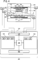
- Fig. 4 illustrates a magnetic resonance imaging system 400 according to a further example outside the scope of the invention.
- the magnetic resonance imaging system 400 shown in Fig. 4 is similar to the magnetic resonance imaging system 300 of Fig. 3 .
- the coil assembly 314 is constructed slightly differently.
- the coil assembly is shown as having multiple coil elements 317. These coil elements 317 are connected to a transmitter 416.
- the coil elements 317 are therefore adapted for irradiating or transmitting radio-frequency energy.
- the transmitter has multiple channels for supplying each of the coil elements 317 with radio-frequency energy separately. Each of the multiple channels may have an individually controllable amplitude and/or phase and/or frequency and/or waveform and/or pulse shape.
- Fig. 6 shows an example of a coil assembly 600 outside the scope of the invention. Again this coil assembly has a first surface 514 and a second surface 516. The first surface is intended to be directed towards an imaging zone of a magnetic resonance imaging system.
- Within the coil assembly 600 there is a collection of coil elements 317. Each of the coil elements 317 is connected to its own individual matching network element 602. The matching network element 602 is connected to a connection to a transceiver 604. Alternatively they may each be connected to a transmitter or receiver also. There may be a separate connection from each matching network element 602 to the transceiver, transmitter, or receiver.
- Also within the coil assembly 600 there is a collection of conductive elements 322 connected by multiple radio-frequency switches 324. The radio-frequency switches 324 are connected to a connection to a radio-frequency shield controller 512.
- the coil elements 317 are between the first surface and the conductive elements 322.
- Embodiments of the invention can easily be realized using common PCB-based coil technology.
- the coil element itself remains unchanged besides the proper tuning compared to the case of no RF-screen present.
- the RF-screen is introduced using typical coil material as well, e.g. copper coated low loss PCB-substrate like FR4.
- the screen is structured e.g. as is shown in Fig. 8 : the slots between the segments in this realization are to be bridged with one or more PIN-diodes in a suitable fashion.
- the diodes are forward biased during transmit shortening the slots and thus forming one RF-screen from the different patches.
- the PIN-diodes are reverse biased isolating the patches from one another. Size and number of patches necessary for a given frequency and coil geometry have to be adapted on case by case basis.
- Fig. 16 illustrates how an embodiment of the invention may be used to protect a portion of a subject 1608.
- a subject 1600 is shown, the subject 1600 is adjacent to a receive coil segment 602.
- the receive coil segment 602 is between the subject and a transmit coil segment 1604.
- On the opposite side of the transmit coil segment 1604 from the receive coil segment 1602 is located a switchable radio-frequency screen 1606.
- the switchable radio-frequency screen 1606 is located between a portion of the subject 1608 and the transmit coil segment 1604.
- the switchable radio-frequency screen 1606 is switched into the closed or blocking state radiation 1610 from the transmit coil segment 1604 is blocked from reaching the shielded portion of the subject 1608.
- Fig. 18 shows an alternative arrangement of the conductive elements 322.
- a radio-frequency shield 1800 is formed by 16 square conductive elements 322.
- Fig. 20 shows an alternative embodiment of a radio-frequency shield 2000 according to an embodiment of the invention.
- the conductive elements 322 are arranged in a target-shape.
- Fig. 21 illustrates how the radio-frequency shield could be constructed using patterned printed circuit board 2100.
- Two pieces of patterned printed circuit board 21 are shown. Each one consists of a low loss substrate 2102. Attached to the low loss substrate 2102 on each board 2100 is patterned copper 2104. Such copper strips 2104 could be used for constructing the antenna elements and/or the conductive elements for the coil assembly.
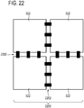
- Fig. 22 shows an alternative embodiment of a radio-frequency shield 2200 according to an embodiment of the invention.
- the conductive elements are connected together with rows of pin diodes 2202.
- the pin diodes 2202 function as the radio-frequency switches.
- This example could be constructed using a printed circuit board with example pin diodes for switching on and off.
- the switches may be replaced by or accompanied by lumped components like capacitors for further expanding the tuning possibilities of the radio-frequency shield 2200.
- Fig. 25 shows an alternative example of a coil assembly 2500 outside the scope of the invention.
- the example of Fig. 25 is similar to that in Figs. 24 and 23 .
- the TEM coil or butterfly coil has been replaced with a loop coil 2502.
- the switchable radio-frequency screen 2704 is between the electronic components 2706 and the coil elements 2702. In case the coil elements 2702 are used to broadcast or transmit radio-frequency energy the switchable radio-frequency screen 2704 can be put into a closed or blocking state in order to protect the electronic components 2706.
- the radio-frequency coils are not decoupled and may have separate switchable radio-frequency screens.
- An electronic component or device such as an S/R switch, preamplifiers, a local radio-frequency amplifier, a PET or positron emission tomography detector is located above the screen.
- a switchable screen protects the electronics during transmit. In case of a geometrical decoupling of the coils for example there is a via overlap, a suitable screen design could be more evolved.
- Embodiments of the invention may have one or more of the following features, provided that the resulting subject-matter falls within the scope of the appended claims:
Description
- The invention relates to magnetic resonance imaging, in particular to a coil assembly with a switchable radio frequency shield.
- A magnetic field is used in Magnetic Resonance (MR) Imaging to align the nuclear spins of atoms as part of the procedure for producing images within the body of a patient. This magnetic field is referred to as the B0 field. During an MR scan, Radio Frequency (RF) pulses generated by a transmitter or amplifier and an antenna cause perturbations to the local magnetic field and can be used to manipulate the orientation of the nuclear spins relative to the B0 field. Radio Frequency (RF) signals emitted by the nuclear spins are detected by a receiver coil, and these RF signals are used to construct the MRI images.
- In most MR-systems to date a volume coil (e.g. quadrature body coil, QBC) is used to transmit the high power signals for spin excitation. For whole body imaging this is the standard setup for up to 3T. For head imaging volume transmitters are applied at 7T and beyond.
- In most such magnetic resonance imaging systems, multichannel receive arrays are employed for improved signal reception and accelerated imaging protocols. This holds true for all anatomies and all field strengths.
- A disadvantage of current multichannel systems is that there may be coupling between the antennas or antenna elements for each channel.
- Prior art RF coil assemblies for MRI with a switchable RF shield are known from
US 5,808,467 ,US 2003/0155918 A1 ,US 2010/0156412 A1 andUS 2009/0251145 A1 . - The invention provides for a coil assembly as defined in claim 1 and a computer program product as defined in claim 13 in the independent claims. Embodiments are given in the dependent claims.
- Embodiments of the invention may address this or other problems by using a switchable radio frequency shield to reduce coupling between antenna elements used to transmit the radio frequency energy.
- Embodiments of the invention may employ a switchable RF-screen to shield and/or decouple transmit/receive (Tx-Rx) surface coils. This may provide several improvements over conventional coils or coil arrays used for Tx-Rx operation: During the transmit phase the RF-screen is switched to a conventional, RF-blocking mode, thus preventing the coil element from radiating a significant amount of its driving RF power. Moreover, a screen close by allows for much easier decoupling of neighboring coil elements, which is beneficial for parallel transmission. Both items mentioned are especially crucial in high field applications.
- During the receive phase, suitable switches (e.g. PIN-diodes) open the RF-screen improving the receive sensitivity of each element. As a by-product, the electric fields, present during transmit phase are successfully suppressed resulting in relaxed SAR performance.
- Some embodiments may use a local RF-screen to local TxRx coils in such a way, that electrical switches (e.g. PIN-diodes) allow for changing the behavior of such a screen. During transmit mode, the switches connect the pieces of the RF-screen such that an RF-blocking behavior is achieved. These results in suppressed radiation losses of the coil during transmit and reduces coupling to neighboring elements which is mandatory for parallel transmit arrays. Furthermore the electrical fields are significantly suppressed improving SAR-behavior of such a coil. The electromagnetic radiation is confined to the requested Field of View (FOV).
- During the receive mode, the switches open the RF-screen segmenting it in several small pieces which are electrically isolated from each other. The sensitivity of the coil element is thus significantly improved compared to the Tx phase allowing for accelerated imaging (e.g. SENSE).
- Embodiments of the invention may address the following problems, especially in high field applications (3T, 7T):
- radiative losses of coils are becoming a major issue
- radiation to body parts outside FOV (back folding, SAR, additional losses, local hot spots located in arms, shoulder parts and head,)
- coupling between coil elements is always a big issue, especially for parallel transmitting applications.
- A 'computer-readable storage medium' as used herein encompasses any tangible storage medium which may store instructions which are executable by a processor of a computing device. The computer-readable storage medium may be referred to as a computer-readable non-transitory storage medium. The computer-readable storage medium may also be referred to as a tangible computer readable medium. In some embodiments, a computer-readable storage medium may also be able to store data which is able to be accessed by the processor of the computing device. Examples of computer-readable storage media include, but are not limited to: a floppy disk, punched tape, punch cards, a magnetic hard disk drive, a solid state hard disk, flash memory, a USB thumb drive, Random Access Memory (RAM), Read Only Memory (ROM), an optical disk, a magneto-optical disk, and the register file of the processor. Examples of optical disks include Compact Disks (CD) and Digital Versatile Disks (DVD), for example CD-ROM, CD-RW, CD-R, DVD-ROM, DVD-RW, or DVD-R disks. The term computer readable-storage medium also refers to various types of recording media capable of being accessed by the computer device via a network or communication link. For example a data may be retrieved over a modem, over the internet, or over a local area network. References to a computer-readable storage medium should be interpreted as possibly being multiple computer-readable storage mediums. Various executable components of a program or programs may be stored in different locations. The computer-readable storage medium may for instance be multiple computer-readable storage medium within the same computer system. The computer-readable storage medium may also be computer-readable storage medium distributed amongst multiple computer systems or computing devices.
- 'Computer memory' or 'memory' is an example of a computer-readable storage medium. Computer memory is any memory which is directly accessible to a processor. Examples of computer memory include, but are not limited to: RAM memory, registers, and register files. References to 'computer memory' or 'memory' should be interpreted as possibly being multiple memories. The memory may for instance be multiple memories within the same computer system. The memory may also be multiple memories distributed amongst multiple computer systems or computing devices.
- 'Computer storage' or 'storage' is an example of a computer-readable storage medium. Computer storage is any non-volatile computer-readable storage medium. Examples of computer storage include, but are not limited to: a hard disk drive, a USB thumb drive, a floppy drive, a smart card, a DVD, a CD-ROM, and a solid state hard drive. In some embodiments computer storage may also be computer memory or vice versa. References to 'computer storage' or 'storage' should be interpreted as possibly being multiple storage mediums or devices. The storage may for instance be multiple storage devices within the same computer system or computing device. The storage may also be multiple storages distributed amongst multiple computer systems or computing devices.
- A 'processor' as used herein encompasses an electronic component which is able to execute a program or machine executable instruction. References to the computing device comprising "a processor" should be interpreted as possibly containing more than one processor or processing core. The processor may for instance be a multi-core processor. A processor may also refer to a collection of processors within a single computer system or distributed amongst multiple computer systems. The term computing device should also be interpreted to possibly refer to a collection or network of computing devices each comprising a processor or processors. Many programs have their instructions performed by multiple processors that may be within the same computing device or which may even be distributed across multiple computing devices.
- A 'user interface' as used herein is an interface which allows a user or operator to interact with a computer or computer system. A 'user interface' may also be referred to as a 'human interface device.' A user interface may provide information or data to the operator and/or receive information or data from the operator. A user interface may enable input from an operator to be received by the computer and may provide output to the user from the computer. In other words, the user interface may allow an operator to control or manipulate a computer and the interface may allow the computer indicate the effects of the operator's control or manipulation. The display of data or information on a display or a graphical user interface is an example of providing information to an operator. The receiving of data through a keyboard, mouse, trackball, touchpad, pointing stick, graphics tablet, joystick, gamepad, webcam, headset, gear sticks, steering wheel, pedals, wired glove, dance pad, remote control, one or more switches, one or more buttons, and accelerometer are all examples of user interface components which enable the receiving of information or data from an operator.
- A 'hardware interface' as used herein encompasses a interface which enables the processor of a computer system to interact with and/or control an external computing device and/or apparatus. A hardware interface may allow a processor to send control signals or instructions to an external computing device and/or apparatus. A hardware interface may also enable a processor to exchange data with an external computing device and/or apparatus. Examples of a hardware interface include, but are not limited to: a universal serial bus, IEEE 1394 port, parallel port, IEEE 1284 port, serial port, RS-232 port, IEEE-488 port, Bluetooth connection, Wireless local area network connection, TCP/IP connection, Ethernet connection, control voltage interface, MIDI interface, analog input interface, and digital input interface.
- Magnetic Resonance (MR) data is defined herein as being the recorded measurements of radio frequency signals emitted by atomic spins by the antenna of a Magnetic resonance apparatus during a magnetic resonance imaging scan. A Magnetic Resonance Imaging (MRI) image is defined herein as being the reconstructed two or three dimensional visualization of anatomic data contained within the magnetic resonance imaging data. This visualization can be performed using a computer.
- In one aspect the invention provides for a magnetic resonance imaging system for acquiring magnetic resonance data from a subject. The magnetic resonance imaging system comprises a magnet for providing an imaging zone. The magnetic resonance imaging system further comprises a coil assembly as defined in claim 1, the coil assembly being configured for eradiating radio-frequency energy into and receiving radio-frequency energy from the imaging zone during the acquisition of the magnetic resonance imaging data. The coil assembly has a first surface configured for being directed towards the imaging zone. The first surface may for instance be the outer surface of the coil assembly which is in contact with the subject. The coil assembly further comprises at least one coil element. The coil element is a radio-frequency coil or antenna element which is configured for eradiating radio-frequency energy. In some embodiments there are multiple coil elements. If there are multiple coil elements each of the coil elements may be configured for eradiating and receiving radio-frequency energy or there may be a combination of some coil elements which are configured for eradiating radio-frequency energy and other coil elements which are configured for receiving radio-frequency energy.
- The coil assembly further comprises a radio-frequency shield switchable between a blocking state and a transparent state. The at least one coil element is between the first surface and the switchable radio-frequency shield. The switchable radio-frequency shield comprises at least two conductive elements. The conductive elements for instance may be surfaces of conductive material. They may for instance be thin films or layers of conductive foil or may be sections of conductive screen. The radio-frequency shield comprises at least one radio-frequency switch configured for electrically connecting the at least two conductive elements when the radio-frequency shield is in the blocking state. The at least one radio-frequency switch is further configured for electrically disconnecting the at least two conductive elements when the radio-frequency shield is in the transparent state.
- When the radio-frequency shield is in the transparent state the attenuation of radio-frequency energy is less than when it is in the blocking state. Essentially the conductive elements in the transparent state are left in a floating or unconnected state. They are sufficiently small that they do not significantly attenuate the radio-frequency energy. However, when the switches are connected then the conductive elements function or act as a larger conductive element. This more effectively blocks radio-frequency energy causing attenuation of the radio-frequency energy to be greater than when it is in the transparent state. In some embodiments when the radio-frequency shield is in the transparent state there is still some attenuation of the radio-frequency energy.
- This embodiment may be beneficial for several different cases. The radio-frequency shield may be used to protect sensitive tissues away from the imaging zone or electronics. When the radio-frequency shield is in the blocking state the tissue and/or electronics are protected. If there are multiple coil elements it may be beneficial to use a radio-frequency shield because it may lead to greater decoupling of the various coil elements.
- According to the invention, the coil assembly is configured for eradiating radio-frequency energy into and for receiving radio-frequency energy from the imaging zone during the acquisition of magnetic resonance imaging. In some embodiments the same coil elements are used for both and in others there are separate coil elements for transmitting and for receiving. The magnetic resonance imaging system further comprises a processor for controlling the operation of the magnetic resonance imaging system. The magnetic resonance imaging system further comprises a memory for storing machine executable instructions for execution by the processor. Execution of the instructions causes the processor to acquire the magnetic resonance data by controlling the magnetic resonance imaging system. Execution of the instructions further causes the processor to switch the radio-frequency shield into the blocking state when eradiating radio-frequency energy by the coil assembly. Execution of the instructions further causes the processor to switch the radio-frequency shield into the transparent state during reception of the radio-frequency transmission by the coil assembly. This embodiment may be beneficial because when the coil assembly is eradiating radio-frequency energy the RF shield contains the region into which the coil assembly is eradiating. Switching the coil assembly into the transparent state may make the coil assembly more sensitive to the radio-frequency transmissions.
- According to the invention, the coil assembly is configured for irradiating radio-frequency energy into the imaging zone during the acquisition of magnetic resonance imaging. The magnetic resonance imaging system further comprises at least one receiver coil configured for receiving radio-frequency signals from atomic spins within the imaging zone during the acquisition of the magnetic resonance data. The magnetic resonance imaging system further comprises a processor for controlling the operation of the magnetic resonance imaging system. The magnetic resonance imaging system further comprises a memory for storing machine executable instructions for execution by the processor. Execution of the instructions causes the processor to acquire the magnetic resonance data by controlling the magnetic resonance imaging system. Execution of the instructions further causes the processor to switch the radio-frequency shield into the blocking state when eradiating radio-frequency energy via the coil assembly. Execution of the instructions further causes the processor to switch the radio-frequency shield into the transparent state during the reception of the radio-frequency coil by the receiver coil. This embodiment may be beneficial because the radio-frequency shield may interfere with the reception of the radio-frequency energy by the receiver coil. By switching it into the transparent state the transmission of the radio-frequency energy through the radio-frequency shield is increased.
- In another embodiment the memory of the magnetic resonance imaging system contains a pulse sequence. The pulse sequence as used herein comprises a set of instructions that are performed at a particular sequence in time in order to operate the magnetic resonance imaging system to acquire magnetic resonance data. The pulse sequence may detail when the radio-frequency shield is switched into the transparent state and when it is switched into the blocking state.
- In another embodiment at least one coil element comprises a controllable matching network element for impedance matching of at least one coil element. The controllable matching network element may be a matching network or a portion of a matching network for impedance matching the coil element. The matching network may be switched between two different impedances or it may be continuously adjustable. Execution of the instructions further causes the processor to adjust the controllable matching network to compensate for the effect of the impedance change of the at least one coil element due to switching the radio-frequency shield between the blocking state and the transparent state.
- In another embodiment the memory further comprises a sensitivity encoding pulse sequence. The magnetic resonance data is acquired by executing the sensitivity encoded pulse sequence. This embodiment may be beneficial because the radio-frequency shield may reduce the coupling between multiple elements in the coil assembly. Sensitivity encoding pulse sequences function by determining the sensitivity of the individual coil elements of a multi-element coil. By reducing the coupling between the individual coil elements the magnetic resonance data acquired with the sensitivity encoded pulse sequence may be more accurate.
- According to the invention, the coil assembly further comprises at least one receiver coil configured for receiving radio-frequency transmissions from atomic spins within the imaging zone during the acquisition of the magnetic resonance data. The radio-frequency shield is located between the at least one coil element and the at least one receiver coil.
- According to the invention, the coil assembly has a second surface configured for receiving a portion of the subject. The second surface is directed away from the imaging zone. The radio-frequency shield is between the second surface and that at least one coil element. The coil assembly has at least two outer surfaces. One surface is directed towards the imaging zone and one is directed away from it. Portions of the subject in contact or in the direction of the second surface will be shielded from radio-frequency energy generated by the coil assembly. This may help to reduce the radio-frequency heating in portions of the subject which are shielded by the radio-frequency shield.
- In another embodiment the radio-frequency switch comprises at least one capacitor configured for tuning the radio-frequency shield to a blocking frequency when the radio-frequency shield is in the blocking state. This for instance may be accomplished by connecting the capacitor between the conductive element and a ground plane or even between two different conductive elements. This embodiment may be advantageous because the radio-frequency shield can be designed for absorbing a specific frequency or band of frequencies very efficiently. This may lead to a better functioning radio-frequency shield.
- In another embodiment the radio-frequency switch comprises a PIN diode.
- In another embodiment the radio-frequency switch comprises a micro electrical mechanical switch or MEMS switch.
- In another embodiment the radio-frequency switch comprises a mechanical relay.
- In another embodiment the coil assembly is further configured such that the at least one coil element is switched to a first resonant frequency when the radio-frequency shield is switched to the blocking state. The coil assembly is further configured such that the at least one coil element is switched to a second resonant frequency when the radio-frequency shield is switched to the transparent state. There will be capacitive coupling between the coil elements and the conductive elements. The amount of capacitance will of course vary between the blocking state and the transparent state. As a result each of the coil elements can be tuned to two specific frequencies that correspond to the switching states. This is particularly true if a capacitor is incorporated into the switch and is used for tuning the conductive elements and/or the coil element.
- In another embodiment the coil assembly comprises multiple coil elements. The radio-frequency shield comprises multiple shield elements each comprising at least two conductive elements. Each of the multiple shield elements is configured for being switched independently between the blocking state and the transparent state. This embodiment is particularly advantageous because the coil elements can be used independently and the degree of coupling between the different coil elements can be controlled by switching between the blocking and the transparent state for the portion of the radio-frequency shield adjacent to each of the conductive elements.
- In another embodiment at least one coil element is a loop coil.
- In another embodiment at least one coil element is a butterfly coil.
- In another embodiment the at least one coil element is a stripline coil.
- In another embodiment the at least one coil element is a TEM transmit coil.
- In another embodiment the at least one coil element is a TEM volume coil.
- In another embodiment the at least one coil element is a TEM coil.
- In another embodiment the at least one coil element is a birdcage coil. The at least one coil element may also be a birdcage volume coil.
- In another embodiment the coil assembly further comprises an electronic component. The radio-frequency shield is between the at least one coil element and the electronic component. The radio-frequency shield is configured for shielding the electronic component from the at least one coil element when the radio-frequency shield is in the blocking state. This embodiment may be advantageous because it may protect sensitive electronics from radio-frequency energy emitted by the at least one coil element. The electronic component may be a positron emission tomography detector, a tuning and matching circuit, an impedance matching network, a preamplifier, an analogue-to-digital converter, and/or a power amplifier.
- In another aspect the invention provides for a coil assembly as defined in claim 1. The advantages of this embodiment have been previously discussed.
- In another aspect the invention provides for a computer program product as defined in claim 13. The advantages of this embodiment have been previously discussed.
- In the following preferred embodiments of the invention will be described, by way of example only, and with reference to the drawings in which:
-
Fig. 1 shows a flow chart which illustrates a method according to an example useful for understanding the invention; -
Fig. 2 shows a flow chart which illustrates a method according to a further example useful for understanding the invention; -
Fig. 3 illustrates a magnetic resonance imaging system; -
Fig. 4 illustrates a magnetic resonance imaging system; -
Fig. 5 illustrates an example of a coil assembly according to an embodiment of the invention; -
Fig. 6 shows a further example of a coil assembly; -
Fig. 7 illustrates how the radio-frequency shield can be used to shield a portion of the subject from radio-frequency energy generated by the coil elements; -
Fig. 8A, 8B, and 8C illustrate a geometry of a radio frequency shield used for a simulation; -
Fig. 9 show simulation results using the geometry illustrated inFigs. 8a, 8b, and 8c ; -
Fig. 10 show simulation results using the geometry illustrated inFigs. 8a, 8b, and 8c ; -
Fig. 11 show simulation results for simulation using a modification of the geometry illustrated inFigs. 8a, 8b, and 8c ; -
Fig. 12 show simulation results for simulation using a modification of the geometry illustrated inFigs. 8a, 8b, and 8c ; -
Fig. 13 illustrate an alternative geometry of a radio frequency shield used for a simulation; -
Fig. 14 show simulation results using the geometry illustrated inFig. 13 ; -
Fig. 15 show simulation results using the geometry illustrated inFig. 13 ; -
Fig. 16 illustrates how an embodiment of the invention may be used to protect a portion of a subject; -
Fig. 17 shows a possible geometry of a radio-frequency shield according to an embodiment of the invention; -
Fig. 18 shows a possible geometry of a radio-frequency shield according to a further embodiment of the invention; -
Fig. 19 shows a possible geometry of a radio-frequency shield according to a further embodiment of the invention; -
Fig. 20 shows a possible geometry of a radio-frequency shield according to a further embodiment of the invention; -
Fig. 21 illustrates how the radio-frequency shield could be constructed using patterned printed circuit board. -
Fig. 22 shows an alternative embodiment of a radio-frequency shield 2200 according to an embodiment of the invention; -
Fig. 23 illustrates a coil assembly; -
Fig. 24 illustrates a coil assembly; -
Fig. 25 illustrates a coil assembly; -
Fig. 26 illustrates a coil assembly; and -
Fig. 27 illustrates an example of the internal components of a coil assembly. - Like numbered elements in these figures are either equivalent elements or perform the same function. Elements which have been discussed previously will not necessarily be discussed in later figures if the function is equivalent.
-
Fig. 1 shows a flow diagram which illustrates a method useful for understanding the invention. Instep 100 magnetic resonance data is acquired. Instep 102 the radio-frequency shield is switched into the blocking state when eradiating radio-frequency energy by the coil assembly. Instep 104 the radio-frequency shield is switched into the transparent state when receiving the radio-frequency energy by the coil assembly. It should be noted thatsteps magnetic resonance data 100. -
Fig. 2 shows a flow diagram which illustrates a further method useful for understanding the invention. Instep 200 magnetic resonance data is acquired. Instep 202 the radio-frequency shield is switched into the blocking state when eradiating radio-frequency energy by the coil assembly. Instep 204 the radio-frequency shield is switched into the transparent state when receiving the radio-frequency energy by the receiver coil. It should be noted thatsteps magnetic resonance data 200. -
Fig. 3 illustrates an example of a magneticresonance imaging system 300 outside the scope of the invention. The magneticresonance imaging system 300 comprises amagnet 304. Themagnet 304 is a superconductingcylindrical type magnet 304 with abore 306 through it. Themagnet 304 has a liquid helium cooled cryostat with superconducting coils. It is also possible to use permanent or resistive magnets. The use of different types of magnets is also possible for instance it is also possible to use both a split cylindrical magnet and a so called open magnet. A split cylindrical magnet is similar to a standard cylindrical magnet, except that the cryostat has been split into two sections to allow access to the iso-plane of the magnet, such magnets may for instance be used in conjunction with charged particle beam therapy. An open magnet has two magnet sections, one above the other with a space in-between that is large enough to receive a subject: the arrangement of the two sections area similar to that of a Helmholtz coil. Open magnets are popular, because the subject is less confined. Inside the cryostat of the cylindrical magnet there is a collection of superconducting coils. Within thebore 306 of thecylindrical magnet 304 there is animaging zone 308 where the magnetic field is strong and uniform enough to perform magnetic resonance imaging. - Within the
bore 306 of the magnet there is also a set of magnetic field gradient coils 310 which is used for acquisition of magnetic resonance data to spatially encode magnetic spins within theimaging zone 308 of themagnet 304. The magnetic field gradient coils 310 connected to a magnetic field gradientcoil power supply 312. The magnetic field gradient coils 310 are intended to be representative. Typically magnetic field gradient coils 310 contain three separate sets of coils for spatially encoding in three orthogonal spatial directions. A magnetic field gradient power supply supplies current to the magnetic field gradient coils. The current supplied to the magnetic field gradient coils 310 is controlled as a function of time and may be ramped or pulsed. - A subject 318 is reposed on a
subject support 320 within thebore 306 of themagnet 304. The subject 318 is partially within theimaging zone 308. In this embodiment acoil assembly 314 is shown as being within theimaging zone 308. In other embodiments the coil assembly could be outside of theimaging zone 308 facing towards the imaging zone. - There is a
first surface 315 of thecoil assembly 314 which is directed towards theimaging zone 308. Thecoil assembly 314 comprises one ormore coil elements 317 and twoconductive elements 322 which are connected by a radio-frequency switch 324. The combination of theconductive elements 322 and the radio-frequency switch 324 form a radio-frequency shield. Thecoil elements 317 are connected to thetransceiver 316. There is a radio-frequency shield controller 325 which is configured for switching the one or more radio-frequency switches 324. Thecoil element 317 may represent multiple coil elements each of which may be driven independently by thetransceiver 316. Likewise the twoconductive elements 322 may represent more than two conductive elements. The radio-frequency switch 324 is also intended to possibly represent multiple radio-frequency switches. The magnetic field gradientcoil power supply 312, thetransceiver 316, and the radio-frequency shield controller 325 are all connected to ahardware interface 328 of acomputer system 326. Thecomputer system 326 further comprises aprocessor 330. Theprocessor 330 is connected to thehardware interface 328, a user interface 334,computer storage 336, andcomputer memory 338. The processor is configured to control the operation and function of the magnetic resonance imaging system using thehardware interface 328. - The
computer storage 336 is shown as containing apulse sequence 340. A pulse sequence as used herein comprises a set of instructions which may be used for temporarily controlling the magneticresonance imaging system 300 to acquiremagnetic resonance data 342. Thecomputer storage 336 is further shown as containingmagnetic resonance data 342 acquired using thepulse sequence 340. Thepulse sequence 340 in some embodiments may be a sensitivity encoding pulse sequence or SENSE pulse sequence. Thecomputer storage 336 is further shown as containing amagnetic resonance image 344 that has been reconstructed from themagnetic resonance data 342. Thecomputer memory 338 is further shown as containing acontrol module 350. Thecontrol module 350 comprises computer executable code for controlling the operation and function of the magneticresonance imaging system 300. It may for instance use thepulse sequence 340 to generate commands to control the magneticresonance imaging system 300 to acquire themagnetic resonance data 342. Thecomputer memory 338 is further shown as containing animage reconstruction module 352 for reconstructing themagnetic resonance image 344 from themagnetic resonance data 342. -
Fig. 4 illustrates a magneticresonance imaging system 400 according to a further example outside the scope of the invention. The magneticresonance imaging system 400 shown inFig. 4 is similar to the magneticresonance imaging system 300 ofFig. 3 . In this example thecoil assembly 314 is constructed slightly differently. The coil assembly is shown as havingmultiple coil elements 317. Thesecoil elements 317 are connected to atransmitter 416. Thecoil elements 317 are therefore adapted for irradiating or transmitting radio-frequency energy. In some examples, the transmitter has multiple channels for supplying each of thecoil elements 317 with radio-frequency energy separately. Each of the multiple channels may have an individually controllable amplitude and/or phase and/or frequency and/or waveform and/or pulse shape. Alternatively, eachcoil element 317 may also be able to be connected to an individual transmitter. Each of the transmitters may have an individually controllable amplitude and/or phase and/or frequency and/or waveform and/or pulse shape. In another embodiment there is only one transmitter and a power combiner distributes the RF energy to the individual coil elements. - The radio-
frequency shield 319 is shown as also comprising threeconductive elements 322 which are connected by radio-frequency switches 324. Again each of themultiple coil elements 317 may each represent multiple coil elements and theconductive elements 322 may also represent further or more conductive elements. Likewise the radio-frequency switch 324 may each represent multiple radio-frequency switches. Mounted in thebore 306 of themagnet 304 is areceiver coil 420. Thereceiver coil 420 is connected to areceiver 418. Thetransmitter 416 and thereceiver 418 are both connected to thehardware interface 328. When thetransmitter 416 is transmitting using thecoil elements 317 theswitches 324 are closed and theconductive elements 322 are connected. When thereceiver 418 is receiving using thereceiver coil 420 theswitches 324 are open and the radio-frequency shield 319 is in the transparent state.Receiver coil 420 may for instance be a body or whole body coil. -
Fig. 5 illustrates an example of acoil assembly 500 according to an embodiment of the invention. The outer surface of thecoil assembly 500 has afirst surface 514 and asecond surface 516. Within thecoil assembly 500 there is a set ofreceiver coil elements 502. Individual coil elements are now shown. In this embodiment there is further a set oftransmitter coil elements 504. The individual transmitter coil elements are not shown. Thereceiver coil elements 502 are between the transmitter coil elements and thefirst surface 514. In this embodiment there is further shown a radio-frequency shield 506 that can be switched between a blocking state and a transparent state. The individual radio-frequency switches and conductive elements comprising the radio-frequency shield 506 are not shown. Thetransmitter coil elements 504 are between the radio-frequency shield 506 and thereceiver coil elements 502. Thereceiver coil elements 502 are shown as being connected to a connection to areceiver 508. Thetransmitter coil elements 504 are shown as being connected to a connection to atransmitter 510. The radio-frequency shield 506 is shown as being connected to a connection to a radio-frequency shield controller 512. -
Fig. 6 shows an example of acoil assembly 600 outside the scope of the invention. Again this coil assembly has afirst surface 514 and asecond surface 516. The first surface is intended to be directed towards an imaging zone of a magnetic resonance imaging system. Within thecoil assembly 600 there is a collection ofcoil elements 317. Each of thecoil elements 317 is connected to its own individualmatching network element 602. Thematching network element 602 is connected to a connection to atransceiver 604. Alternatively they may each be connected to a transmitter or receiver also. There may be a separate connection from eachmatching network element 602 to the transceiver, transmitter, or receiver. Also within thecoil assembly 600 there is a collection ofconductive elements 322 connected by multiple radio-frequency switches 324. The radio-frequency switches 324 are connected to a connection to a radio-frequency shield controller 512. Thecoil elements 317 are between the first surface and theconductive elements 322. -
Fig. 7 illustrates how the radio-frequency shield 704 can be used to shield a portion of the subject 708 from radio-frequency energy generated by thecoil elements 702. In this Fig. there is acoil assembly 700. It has afirst surface 514 directed towards animaging zone 308 of a magnetic resonance imaging system. It has asecond surface 516 directed away from theimaging zone 308. There is a subject 318 partially within theimaging zone 706. In thecoil assembly 700 there are one ormore coil elements 702 that are between thefirst surface 514 and the radio-frequency shield 704. The individual conductive elements and switches of the radio-frequency shield 704 are not illustrated in this example. The region of the subject 706 may be imaged in the magnetic resonance imaging system. Theregion 708 of the subject 318 is shielded by the radio-frequency shield 704 from thecoil elements 702. -
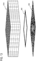
Figs. 8a, 8b, and 8c illustrate a geometry for a simulation. There is asingle loop coil 800 which functions as the coil element. This is shown inFigs. 8a, 8b and 8c. Fig. 8b also shows fourconductive elements 802. The radio-frequency screen is in the open or in transparent mode. Finally inFig. 8c the fourconductive elements 802 are connected together to make a radio-frequency shield 804 that is in the blocking state. - Embodiments of the invention can easily be realized using common PCB-based coil technology. The coil element itself remains unchanged besides the proper tuning compared to the case of no RF-screen present. The RF-screen is introduced using typical coil material as well, e.g. copper coated low loss PCB-substrate like FR4. The screen is structured e.g. as is shown in
Fig. 8 : the slots between the segments in this realization are to be bridged with one or more PIN-diodes in a suitable fashion. The diodes are forward biased during transmit shortening the slots and thus forming one RF-screen from the different patches. During receive mode the PIN-diodes are reverse biased isolating the patches from one another. Size and number of patches necessary for a given frequency and coil geometry have to be adapted on case by case basis. - In an alternative embodiment to that shown in
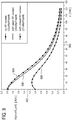
Figs. 8a, 8b, and 8c , the slots in the RF-screen are equipped with lumped capacitances of a predetermined value that are switched active with PIN-diodes. Doing so results in a resonant RF-screen. The resonance frequency of the screen may be shifted using tunable caps e.g. varactors or preset fixed values. This setup allows for adjusting the amount of coupling between RF-screen and coil element and via this adjustment the behavior of the B1- and E-fields. InFigs. 8a, 8b, and 8c the local electrical field in arepresentative triangle 10 mm above a capacitor for the surface coil (no dielectric) with and without a RF shield related to the same B1 at a distance of 100mm from the coil was calculated using the geometry shown inFig. 8 . The RF current increases from 469 A/m to 1237A/m, which corresponds to a factor of 2.638. The electrical field increases 10mm above a capacitor from 3.98kV/m to 6.54kV/m, thus the increase is only a factor of 1.64. The results are shown inFigs. 9 and10 . -
Figs. 9 and10 show simulation results using the geometry illustrated inFigs. 8a, 8b, and 8c . InFig. 9 themagnetic field component 902 is shown as a function ofdistance 900 for three cases with no radio-frequency screen 904, with the open or transparent radio-frequency screen 906, and with the closed or blocking radio-frequency screen 908. -
Fig. 9 plots the magnitude of the H-field on the z-axis for the three different scenarios for equal excitation power of 1W.Fig. 9 demonstrates, that the slitted RF-shield does not significantly suppress the magnitude of the H-field achievable. The opened RF-shield would be used during reception.Fig. 10 shows the corresponding E-field along the z-axis. During transmission, the RF-shield would be closed e.g. using PIN-diodes significantly reducing E-fields. The RF-screen is located 20mm below the coil, the central opening (c.f.Fig. 8 is 20x20mm). -
Figs. 11 and12 show results similar to those shown inFigs. 9 and10 except for the simulation distance to the radio-frequency screen was reduced to 10mm and the radio-frequency screen was completely closed not containing a hole in the center as is shown inFigs. 8b and 8c . The reduction in the electric field for the transmitting state is even better than in comparison to the results shown inFigs. 9 and10 . - In
Figs. 11 and12 , results from simulations as inFigs. 9 and10 with different geometry are shown. The distance to the RF-screen was reduced to 10mm and the RF-screen was completely closed, not containing the hole in the center (cf.Fig. 8 ). The reduction in E-field for Tx is even better compared toFigs. 9 and10 . -
Fig. 13 shows a different simulation geometry. The geometry shown inFigs. 8a, b and c is used again except in this case thecoil 800 and the switchable radio-frequency screen 804 are loaded with adielectric body 1300. Thecoil 800 is located adjacent to thedielectric body 1300. Thedielectric body 1300 is to simulate the effect of human tissue located 10mm about the radio-frequency coil. -
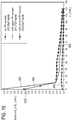
Figs. 14 and15 are analogous toFigs. 9 and10 except the simulation geometry ofFig. 13 is used instead of the simulation geometry ofFigs. 8a, 8b, and 8c . These results show simulations as described above with a isotropic dielectric having properties of human tissue located 10mm above the RF-coil. The reduction of E-fields close to the coil during transmission is significantly reduced while the required power for equal magnetic field is doubled. -
Fig. 16 illustrates how an embodiment of the invention may be used to protect a portion of a subject 1608. In this Fig. a subject 1600 is shown, the subject 1600 is adjacent to a receivecoil segment 602. The receivecoil segment 602 is between the subject and a transmitcoil segment 1604. On the opposite side of the transmitcoil segment 1604 from the receivecoil segment 1602 is located a switchable radio-frequency screen 1606. The switchable radio-frequency screen 1606 is located between a portion of the subject 1608 and the transmitcoil segment 1604. When the switchable radio-frequency screen 1606 is switched into the closed or blockingstate radiation 1610 from the transmitcoil segment 1604 is blocked from reaching the shielded portion of the subject 1608. - In the embodiment shown in
Fig. 16 and according to the invention, different coil elements are used for Transmit (Tx) and Receive (Rx). While the Tx onlycoil 1604 is located close to the screen (as described above) the Rx only is located closer to the subject to be imaged (and thus farther from the RF-screen). This results in improved Rx sensitivities but on the cost of a thicker batch of coils/screen. -
Fig. 17 shows a possible geometry of a radio-frequency shield 1700 according to an embodiment of the invention. In this embodiment there are four squareconductive elements 322 arranged next to each other. -
Fig. 18 shows an alternative arrangement of theconductive elements 322. In this Fig. a radio-frequency shield 1800 is formed by 16 squareconductive elements 322. -
Fig. 19 shows a radio-frequency shield 1900 according to a further embodiment of the invention. In this embodiment the radio-frequency shield is circular-shaped and is comprised of pie-shapedconductive elements 322. -
Fig. 20 shows an alternative embodiment of a radio-frequency shield 2000 according to an embodiment of the invention. In this embodiment theconductive elements 322 are arranged in a target-shape. - Examples shown in
Figs. 17, 18 ,19, and 20 are only several possible designs for a structured radio-frequency screen depending on the desired influence on the radio-frequency coil located above such a screen. Irregular shapes are also possible and may be desirable for certain applications. -
Fig. 21 illustrates how the radio-frequency shield could be constructed using patterned printedcircuit board 2100. Two pieces of patterned printed circuit board 21 are shown. Each one consists of alow loss substrate 2102. Attached to thelow loss substrate 2102 on eachboard 2100 is patternedcopper 2104.Such copper strips 2104 could be used for constructing the antenna elements and/or the conductive elements for the coil assembly. -
Fig. 22 shows an alternative embodiment of a radio-frequency shield 2200 according to an embodiment of the invention. In this example there are fourconductive elements 322. The conductive elements are connected together with rows ofpin diodes 2202. Thepin diodes 2202 function as the radio-frequency switches. This example could be constructed using a printed circuit board with example pin diodes for switching on and off. In some embodiments the switches may be replaced by or accompanied by lumped components like capacitors for further expanding the tuning possibilities of the radio-frequency shield 2200. -
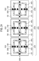
Fig. 23 illustrates acoil assembly 2200 according to an example outside the scope of the invention. This coil assembly has three separate radio-frequency shields 2304. Each of the separate radio-frequency shields 2304 is comprised of fourconductive elements 322 that are connected bypin diodes 2202. For each of the separate radio-frequency shields 2304 there is a TEM transmitcoil 2302. The TEM transmit coils are not decoupled and have separate switchable radio-frequency screens 2304. During transmit the coils are connected with the screen and the transmit coil is resonant. During reception a separate loop coil is located below the screen which is not shown. In case of geometrical decoupling of the coils, for example via overlap a suitable screen design would be more evolved. The TEM transmit coils are connected to the screen viapin diodes 2202. -
Fig. 24 shows another example of acoil assembly 2400 outside the scope of the invention. The example shown inFig. 24 is very similar to that shown inFig. 23 except that butterfly coils 2402 are used instead of the TEM transmit coils. The butterfly coils 2402 are split withpin diodes 2202. When the butterfly coils 2402 are used for transmitting or receiving the pin diodes are used to connect the two sections of the butterfly coils 2402. -
Fig. 25 shows an alternative example of acoil assembly 2500 outside the scope of the invention. The example ofFig. 25 is similar to that inFigs. 24 and23 . However, in this case the TEM coil or butterfly coil has been replaced with aloop coil 2502. -
Fig. 26 shows a coil assembly according to an alternative example outside the scope of the invention. Thecoil assembly 2600 shown inFig. 26 is similar to that ofFig. 25 except all of theconductive elements 322 are connected bypin diodes 2202. There are no separate radio-frequency shields in this example there is just one large radio-frequency shield. -
Fig. 27 shows an example of the internal components of acoil assembly 2700 according to an example outside the scope of the invention. There is a collection ofcoil elements 2702. - There is also a switchable radio-
frequency screen 2704 adjacent to thecoil elements 2702. Also shown are a collection of sensitiveelectronic components 2706. The switchable radio-frequency screen 2704 is between theelectronic components 2706 and thecoil elements 2702. In case thecoil elements 2702 are used to broadcast or transmit radio-frequency energy the switchable radio-frequency screen 2704 can be put into a closed or blocking state in order to protect theelectronic components 2706. The radio-frequency coils are not decoupled and may have separate switchable radio-frequency screens. An electronic component or device such as an S/R switch, preamplifiers, a local radio-frequency amplifier, a PET or positron emission tomography detector is located above the screen. A switchable screen protects the electronics during transmit. In case of a geometrical decoupling of the coils for example there is a via overlap, a suitable screen design could be more evolved. - Embodiments of the invention may have one or more of the following features, provided that the resulting subject-matter falls within the scope of the appended claims:
- 1. Switchable RF screen or conductor pattern, which results in an influence on the field pattern of an RF coil
- 2. RF screen consists of PCB or conductor material and is structured
- 3. Screening conductor element is passive or can be made partly resonant to provide a higher screening effect. This is achieved by series capacitors (discrete or distributed)
- 4. The coil setup can have an additional receive coil layer.
- 5. Receive coil layer can be externally mechanically connected and supplied via common galvanic or optical or inductive, wireless connection.
- 6. Individual RF screen elements are electromagnetically separated (low impedance) to suppress waveguide effects and thus uncontrollable mode patterns and SAR values
- 7. PIN or MEM switching electronics.
- 8. Arrangement with described characteristics such as Flex L,M,S as transmit tx/rx array
- 9. Arrangement with described characteristics for combined Tx/Rx arrays consisting of loop and TEM stripline structures.
- 10. Coil element with electronic retuning device to compensate switching shield effect.
- 11. Double resonant coil element, with switchable screen. The coil element does not require a PIN switch, as 2nd resonance is tuned by shield to MR resonance frequency.
- While the invention has been illustrated and described in detail in the drawings and foregoing description, such illustration and description are to be considered illustrative or exemplary and not restrictive; the invention is solely defined by the appended claims and is not limited to the disclosed embodiments.
- Other variations to the disclosed embodiments can be understood and effected by those skilled in the art in practicing the claimed invention, from a study of the drawings, the disclosure, and the appended claims. In the claims, the word "comprising" does not exclude other elements or steps, and the indefinite article "a" or "an" does not exclude a plurality. A single processor or other unit may fulfill the functions of several items recited in the claims. The mere fact that certain measures are recited in mutually different dependent claims does not indicate that a combination of these measured cannot be used to advantage. A computer program may be stored/distributed on a suitable medium, such as an optical storage medium or a solid-state medium supplied together with or as part of other hardware, but may also be distributed in other forms, such as via the Internet or other wired or wireless telecommunication systems. Any reference signs in the claims should not be construed as limiting the scope.
-
- 300
- magnetic resonance imaging system
- 304
- magnet
- 306
- bore of magnet
- 308
- imaging zone
- 310
- magnetic field gradient coils
- 312
- magnetic field gradient coil power supply
- 314
- coil assembly
- 315
- first surface
- 316
- transceiver
- 317
- coil elements
- 318
- subject
- 319
- radio frequency shield
- 320
- subject support
- 322
- conductive element
- 324
- radio frequency switch
- 325
- radio frequency shield controller
- 326
- computer system
- 328
- hardware interface
- 330
- processor
- 332
- user interface
- 334
- user interface
- 336
- computer storage
- 338
- computer memory
- 340
- pulse sequence (sensitivity encoding pulse sequence)
- 342
- magnetic resonance data
- 344
- magnetic resonance image
- 350
- control module
- 352
- image reconstruction module
- 400
- magnetic resonance imaging system
- 416
- transmitter
- 418
- receiver
- 420
- receiver coil
- 500
- coil assembly
- 502
- receiver coil elements
- 504
- transmitter coil elements
- 506
- radio frequency shield
- 508
- connection to receiver
- 510
- connection to transmitter
- 512
- connection to radio frequency shield controller
- 514
- first surface
- 516
- second surface
- 600
- coil assembly
- 602
- matching network element
- 604
- connection to transceiver
- 700
- coil assembly
- 702
- coil elements
- 704
- radio frequency shield
- 706
- portion of subject within imaging zone
- 708
- shielded portion of subject
- 900
- distance
- 902
- magnetic field component
- 904
- no-RF screen
- 906
- with open or transparent RF screen
- 908
- with closed RF screen
- 1002
- Electric field component
- 1600
- subject
- 1602
- receive coil segment
- 1604
- transmit coil segment
- 1606
- switchable radio frequency screen
- 1608
- shielded portion of subject
- 1610
- radiation prevented by RF screen
- 1700
- radio frequency shield
- 1800
- radio frequency shield
- 1900
- radio frequency shield
- 2000
- radio frequency shield
- 2100
- patterned printed circuit board
- 2102
- low loss substrate
- 2104
- copper
- 2200
- radio frequency shield
- 2202
- PIN diodes
- 2300
- coil assembly
- 2302
- TEM transmit coils
- 2304
- separate radio frequency shield
- 2400
- coil assembly
- 2402
- butterfly coil
- 2500
- coil assembly
- 2502
- loop coil
- 2600
- coil assembly
- 2700
- coil assembly
- 2702
- coil elements
- 2704
- switchable RF screen
- 2706
- electronic component
Claims (13)
- A coil assembly (319, 500, 600, 700, 2700) for radiating radio frequency energy and receiving radio frequency energy during the acquisition of magnetic resonance data (342), wherein the coil assembly has a first surface (315, 514) configured for being directed towards an imaging zone (308) of a magnetic resonance imaging system (300, 400),
wherein the coil assembly further comprises at least one coil element (317, 502, 504, 702, 800, 1602, 1604, 2302, 2402, 2502, 2702), wherein the coil assembly further comprises a radio frequency shield (319, 506, 704, 1700, 1800, 1900, 2000, 2200, 2304, 2704) switchable between a radio-frequency blocking state (804) and a radio-frequency transparent state (802), wherein the at least one coil element is between the first surface and the radio frequency shield, wherein the radio frequency shield comprises at least two conductive elements (322, 802, 804), wherein the radio frequency shield comprises a radio frequency switch (324, 2202) configured for electrically connecting the at least two conductive elements when the radio frequency shield is in the radio-frequency blocking state, wherein the radio frequency switch is further configured for electrically disconnecting the at least two conductive elements when the radio frequency shield is in the radio-frequency transparent state, wherein the coil assembly further comprises at least one receiver coil (502, 1602) configured for receiving radio frequency transmissions from atomic spins within the imaging zone during the acquisition of the magnetic resonance data, wherein the at least one coil element is a transmitter coil element and is located between the radio frequency shield and the at least one receiver coil, wherein the coil assembly has a second surface (516) configured for receiving a portion (708) of the subject, wherein the second surface is directed away from the imaging zone, and wherein the radio frequency shield is between the second surface and the at least one coil element. - A magnetic resonance imaging system (300, 400) for acquiring magnetic resonance data (342) from a subject (318), wherein the magnetic resonance imaging system comprises:- a magnet (304) for providing an imaging zone (308); and- a coil assembly (319, 500, 600, 700, 2700) according to claim 1 configured for radiating radio frequency energy into the imaging zone and receiving radio frequency energy from the imaging zone during the acquisition of the magnetic resonance imaging data.
- The magnetic resonance imaging system of claim 2, wherein the magnetic resonance imaging system further comprises:- a processor (330) for controlling the operation of the magnetic resonance imaging system;- a memory (338) for storing machine executable instructions for execution by the processor, wherein execution of the instructions causes the processor to:- acquire (100) the magnetic resonance data by controlling the magnetic resonance imaging system;- switch (102) the radio frequency shield into the radio-frequency blocking state when radiating radio frequency energy by the coil assembly; and- switch (104) the radio frequency shield into the radio-frequency transparent state during reception of the radio frequency transmissions by the coil assembly.
- The magnetic resonance imaging system of claim 2, wherein the magnetic resonance imaging system further comprises:- a processor (330) for controlling the operation of the magnetic resonance imaging system;- a memory (338) for storing machine executable instructions for execution by the processor, wherein execution of the instructions causes the processor to:- acquire (200) the magnetic resonance data by controlling the magnetic resonance imaging system;- switching (202) the radio frequency shield into the radio-frequency blocking state when radiating radio frequency energy by the coil assembly; and- switching (204) the radio frequency shield into the radio-frequency transparent state during reception of the radio frequency energy by the receiver coil.
- The magnetic resonance imaging system of claim 3 or 4, wherein at least one coil element comprises a controllable matching network element (602) for impedance matching of at least one coil element, wherein execution of the instructions further causes the processor to adjust the controllable matching network to compensate for the effect of the impedance change of the at least one coil element due to switching the radio frequency shield between the radio-frequency blocking state and the radio-frequency transparent state.
- The magnetic resonance imaging system of claim 3, 4, or 5, wherein the memory further comprises a sensitivity encoding pulse sequence (340), wherein the magnetic resonance data is acquired by executing the sensitivity encoding pulse sequence.
- The magnetic resonance imaging system of any one of preceding claims 2-6, wherein the radio frequency switch comprises at least one capacitor configured for tuning the radio frequency shield to a blocking frequency when the radio frequency shield is in the radio-frequency blocking state.
- The magnetic resonance imaging system of any one of preceding claims 2-7, wherein the radio frequency switch comprises any one of the following: a PIN diode, micro electromechanical switch, and a mechanical relays.
- The magnetic resonance imaging system of any one of preceding claims 2-8, wherein the coil assembly is further configured such that the at least one coil element is switched to a first resonant frequency when the radio frequency shield is switched to the radio-frequency blocking state, and wherein the coil assembly is further configured such that the at least one coil element is switched to a second resonant frequency when the radio frequency shield is switched to the radio-frequency transparent state.
- The magnetic resonance imaging system of any one of preceding claims 2-9, wherein the coil assembly (2300, 2400, 2500) comprises multiple coil elements (2302, 2202, 2502), wherein the radio frequency shield comprises multiple shield elements each comprising at least two conductive elements, wherein each of the multiple shield elements is configured for being switched independently between the radio-frequency blocking state and the radio-frequency transparent state.
- The magnetic resonance imaging system of any one of preceding claims 2-10, wherein the at least one coil element is any one of the following: a loop coil (800), a butterfly coil (2202), a stripline coil, a TEM transmit coil (2302), a TEM volume coil, a TEM coil, and a birdcage coil.
- The magnetic resonance imaging system of any one of preceding claims 2-11, wherein the coil assembly further comprises an electronic component (2706), wherein the radio frequency shield is between the at least one coil element and the electronic component, wherein the radio frequency shield is configured for shielding the electronic component from the at least one coil element.
- A computer program product comprising machine executable code (350, 352) for execution by a processor (330) controlling a magnetic resonance imaging system (300, 400), wherein the magnetic resonance imaging system comprises a magnet (304) for providing an imaging zone (308), wherein the magnetic resonance imaging system further comprises a coil assembly according to claim 1, wherein the coil assembly is configured for radiating radio frequency energy and for receiving radio frequency energy, and wherein execution of the instructions causes the processor to:- acquire (100) magnetic resonance data by controlling the magnetic resonance imaging system;- switch (102) the radio frequency shield into the radio-frequency blocking state when radiating radio frequency energy by the coil assembly; and- switch (104) the radio frequency shield into the radio-frequency transparent state during reception of the radio frequency transmissions. by the coil assembly.
Applications Claiming Priority (2)
| Application Number | Priority Date | Filing Date | Title |
|---|---|---|---|
| US201161548287P | 2011-10-18 | 2011-10-18 | |
| PCT/IB2012/055289 WO2013057612A1 (en) | 2011-10-18 | 2012-10-03 | Mri coil assembly with a radio frequency shield switchable between a blocking state and a transparent state |
Publications (2)
| Publication Number | Publication Date |
|---|---|
| EP2745132A1 EP2745132A1 (en) | 2014-06-25 |
| EP2745132B1 true EP2745132B1 (en) | 2020-12-09 |
Family
ID=47192031
Family Applications (1)
| Application Number | Title | Priority Date | Filing Date |
|---|---|---|---|
| EP12787879.1A Active EP2745132B1 (en) | 2011-10-18 | 2012-10-03 | Mri coil assembly with a radio frequency shield switchable between a blocking state and a transparent state |
Country Status (8)
| Country | Link |
|---|---|
| US (1) | US9869735B2 (en) |
| EP (1) | EP2745132B1 (en) |
| JP (1) | JP6033320B2 (en) |
| CN (1) | CN103959085B (en) |
| IN (1) | IN2014CN02544A (en) |
| MX (1) | MX2014004533A (en) |
| RU (1) | RU2595798C2 (en) |
| WO (1) | WO2013057612A1 (en) |
Families Citing this family (21)
| Publication number | Priority date | Publication date | Assignee | Title |
|---|---|---|---|---|
| DE102012203331B4 (en) * | 2012-03-02 | 2015-08-27 | Siemens Aktiengesellschaft | Local screen and method for shielding magnetic resonance signals |
| EP2672286A1 (en) * | 2012-06-05 | 2013-12-11 | Koninklijke Philips N.V. | TEM resonator system especially for use in an MRI system |
| JP6349320B2 (en) * | 2012-11-05 | 2018-06-27 | コーニンクレッカ フィリップス エヌ ヴェKoninklijke Philips N.V. | Transmission / reception switching circuit with improved radio frequency separation |
| CN105308471B (en) * | 2013-06-17 | 2018-12-18 | 皇家飞利浦有限公司 | Magnetic resonance imaging subject supporter |
| JP2017502727A (en) * | 2013-12-10 | 2017-01-26 | コーニンクレッカ フィリップス エヌ ヴェKoninklijke Philips N.V. | Calculation of RF coil sensitivity of MRI using interpolation to enlarged field of view |
| DE102014207843B4 (en) * | 2014-04-25 | 2019-06-27 | Siemens Healthcare Gmbh | Knee Coil |
| US10172575B2 (en) * | 2014-09-16 | 2019-01-08 | Koninklijke Philips N.V. | Protection system for protecting a person against X-ray scatter radiation |
| DE102015201462B3 (en) * | 2015-01-28 | 2016-05-12 | Siemens Aktiengesellschaft | High frequency coil unit for magnetic resonance imaging |
| US10877114B2 (en) * | 2016-10-10 | 2020-12-29 | Koninklijke Philips N.V. | Co-planar RF coil feeding |
| DE102017214088A1 (en) * | 2017-08-11 | 2019-02-14 | Siemens Healthcare Gmbh | Image data generation in an examination room of an MR system |
| US11564575B2 (en) * | 2018-01-17 | 2023-01-31 | Shanghai United Imaging Healthcare Co., Ltd. | Magnetic resonance-positron emission tomography imaging apparatus |
| CN108761365B (en) * | 2018-04-11 | 2021-02-19 | 上海联影医疗科技股份有限公司 | Shielding shell, manufacturing method of shielding shell, PET detector and system |
| US10598739B2 (en) * | 2018-06-18 | 2020-03-24 | Allegro Microsystems, Llc | Magnetic field sensors having virtual signals |
| US10866118B2 (en) | 2018-06-18 | 2020-12-15 | Allegro Microsystems, Llc | High resolution magnetic field sensors |
| US10908229B2 (en) | 2018-06-18 | 2021-02-02 | Allegro Microsystems, Llc | Regulation of coefficients used in magnetic field sensor virtual signal generation |
| US10578679B2 (en) * | 2018-06-18 | 2020-03-03 | Allegro Microsystems, Llc | Magnetic field sensors having virtual signals |
| US10684336B2 (en) | 2018-10-24 | 2020-06-16 | General Electric Company | Radiofrequency coil and shield in magnetic resonance imaging method and apparatus |
| US10859648B2 (en) * | 2019-04-01 | 2020-12-08 | GE Precision Healthcare LLC | Systems and methods for a configurable radio frequency coil for MR imaging |
| CN111965577B (en) * | 2020-07-07 | 2023-07-28 | 无锡鸣石峻致医疗科技有限公司 | Multi-frequency coil |
| CN112540332B (en) * | 2020-12-03 | 2023-11-14 | 深圳航天科技创新研究院 | Magnetic resonance radio frequency shielding structure and design method thereof |
| US11762043B2 (en) | 2021-03-11 | 2023-09-19 | Allegro Microsystems, Llc | High resolution magnetic field sensors |
Family Cites Families (26)
| Publication number | Priority date | Publication date | Assignee | Title |
|---|---|---|---|---|
| CN1009140B (en) * | 1985-04-01 | 1990-08-08 | 菲利浦光灯制造公司 | Produce and/or receive the rf coil system of alternating magnetic field |
| JPH0349737A (en) * | 1989-07-18 | 1991-03-04 | Toshiba Corp | Magnetic resonance imaging device |
| US5132621A (en) * | 1990-04-24 | 1992-07-21 | General Electric Company | Radio frequency field coil and power splitter for nmr |
| US5406204A (en) | 1992-03-27 | 1995-04-11 | Picker International, Inc. | Integrated MRI gradient coil and RF screen |
| JPH07155307A (en) * | 1993-12-09 | 1995-06-20 | Hitachi Ltd | Rf coil for mri and mri device |
| US5419325A (en) * | 1994-06-23 | 1995-05-30 | General Electric Company | Magnetic resonance (MR) angiography using a faraday catheter |
| JP3492009B2 (en) * | 1995-03-16 | 2004-02-03 | ジーイー横河メディカルシステム株式会社 | MRI coil device |
| US5808467A (en) * | 1995-05-31 | 1998-09-15 | Hitachi, Ltd. | RF probe and inspection system using NMR using the same |
| US5760584A (en) * | 1996-08-16 | 1998-06-02 | General Electric Company | Shield for MR system RF coil provided with multiple capacitive channels for RF current flow |
| JPH11299754A (en) * | 1998-04-23 | 1999-11-02 | Toshiba Iyo System Engineering Kk | Divisible rf coil for mri apparatus |
| JP3457537B2 (en) * | 1998-06-30 | 2003-10-20 | 株式会社東芝 | Magnetic resonance imaging |
| US6437567B1 (en) * | 1999-12-06 | 2002-08-20 | General Electric Company | Radio frequency coil for open magnetic resonance imaging system |
| GB2360094A (en) * | 2000-03-06 | 2001-09-12 | Marconi Caswell Ltd | RF screens for MRI |
| US6522144B2 (en) | 2000-12-22 | 2003-02-18 | Ge Medical Systems Global Technology Company, Llc | RF shielding method and apparatus for an open MRI system |
| US6498947B2 (en) | 2001-02-23 | 2002-12-24 | Ge Medical Systems Global Technology Company, Llc | rf shielding method and apparatus |
| US20050107681A1 (en) * | 2003-07-23 | 2005-05-19 | Griffiths David M. | Wireless patient monitoring device for magnetic resonance imaging |
| US7053617B2 (en) | 2003-10-01 | 2006-05-30 | General Electric Co. | Integrated electronic RF shielding apparatus for an MRI magnet |
| CN100554993C (en) * | 2003-11-18 | 2009-10-28 | 皇家飞利浦电子股份有限公司 | The RF coil system that is used for super high field (SHF) MRI |
| JP2006346055A (en) * | 2005-06-15 | 2006-12-28 | Hitachi Medical Corp | Testing apparatus using magnetic resonance |
| JP2007260078A (en) * | 2006-03-28 | 2007-10-11 | Ge Medical Systems Global Technology Co Llc | Rf coil, and magnetic resonance imaging system |
| US8159223B2 (en) * | 2006-12-22 | 2012-04-17 | Koninklijke Philips Electronics N.V. | RF coil for use in an MR imaging system |
| EP2115485A1 (en) * | 2007-02-26 | 2009-11-11 | Koninklijke Philips Electronics N.V. | Doubly resonant high field radio frequency surface coils for magnetic resonance |
| JP5103640B2 (en) * | 2007-04-13 | 2012-12-19 | 株式会社日立メディコ | Magnetic resonance imaging system |
| JP5247214B2 (en) * | 2008-04-04 | 2013-07-24 | 株式会社日立製作所 | High frequency magnetic field coil and magnetic resonance imaging apparatus |
| DE102008063457B3 (en) * | 2008-12-17 | 2010-06-02 | Siemens Aktiengesellschaft | Local coil arrangement for magnetic resonance applications with activatable marker |
| CN102652027B (en) | 2009-12-10 | 2014-11-26 | 皇家飞利浦电子股份有限公司 | Magnetic resonance -compatible electrical device with radio frequency shielding or an enclosure |
-
2012
- 2012-10-03 WO PCT/IB2012/055289 patent/WO2013057612A1/en active Application Filing
- 2012-10-03 MX MX2014004533A patent/MX2014004533A/en not_active Application Discontinuation
- 2012-10-03 IN IN2544CHN2014 patent/IN2014CN02544A/en unknown
- 2012-10-03 US US14/352,030 patent/US9869735B2/en active Active
- 2012-10-03 EP EP12787879.1A patent/EP2745132B1/en active Active
- 2012-10-03 RU RU2014119865/28A patent/RU2595798C2/en active
- 2012-10-03 JP JP2014536357A patent/JP6033320B2/en active Active
- 2012-10-03 CN CN201280051019.8A patent/CN103959085B/en active Active
Non-Patent Citations (1)
| Title |
|---|
| None * |
Also Published As
| Publication number | Publication date |
|---|---|
| JP2014530079A (en) | 2014-11-17 |
| RU2595798C2 (en) | 2016-08-27 |
| CN103959085B (en) | 2017-03-08 |
| US9869735B2 (en) | 2018-01-16 |
| CN103959085A (en) | 2014-07-30 |
| WO2013057612A1 (en) | 2013-04-25 |
| US20140253122A1 (en) | 2014-09-11 |
| MX2014004533A (en) | 2014-08-01 |
| JP6033320B2 (en) | 2016-11-30 |
| EP2745132A1 (en) | 2014-06-25 |
| RU2014119865A (en) | 2015-11-27 |
| IN2014CN02544A (en) | 2015-07-31 |
Similar Documents
| Publication | Publication Date | Title |
|---|---|---|
| EP2745132B1 (en) | Mri coil assembly with a radio frequency shield switchable between a blocking state and a transparent state | |
| KR100677021B1 (en) | Rf body coil | |
| US9116214B2 (en) | RF coil array having two or more switches built within each RF coil array element, compatible with both magnetic resonance and a temperature mapping | |
| EP3523667B1 (en) | Impedance matching using multiple rf ports | |
| EP1883348B1 (en) | Antenna device for picking up magnetic resonance signals and provided with its own communication unit | |
| EP3123189B1 (en) | Magnetic resonance imaging rf antenna | |
| WO2010045457A2 (en) | Coil element decoupling for mri | |
| US10877116B2 (en) | Birdcage magnetic resonance imaging (MRI) coil with open shield for single tune MRI coil and multi-tune MRI coil | |
| CN110168393A (en) | The magnetic resonance tomography equipment run under low magnetic field intensity and local coil matrix | |
| Zhang et al. | Effect of radiofrequency shield diameter on signal‐to‐noise ratio at ultra‐high field MRI | |
| Adriany et al. | Evaluation of a 16-channel transmitter for head imaging at 10.5 T | |
| EP2856194B1 (en) | System of tem resonators for use in an mri system | |
| US10444312B2 (en) | Magnetic resonance imaging system | |
| Ruytenberg et al. | Design of a dielectric resonator receive array at 7 Tesla using detunable ceramic resonators | |
| US20100109667A1 (en) | Transverse electromagnetic radio-frequency coil | |
| WO2017050605A1 (en) | Radio frequency antenna assembly for magnetic resonance image guided therapy | |
| EP3387456B1 (en) | Radio frequency coil-array for magnetic resonance examination system | |
| US8436615B2 (en) | Detunable waveguide antenna assembly | |
| Woo et al. | A monopole and dipole hybrid antenna array for human brain imaging at 10.5 Tesla | |
| Nikulin et al. | Reconfigurable dipole receive array for dynamic parallel imaging at ultra‐high magnetic field | |
| Vaughan et al. | Ultra high field MRI: high-frequency coils | |
| EP4303604A1 (en) | Receiving coil | |
| US20230280424A1 (en) | Field modification device | |
| WO2005122890A1 (en) | Mr device volume coil | |
| Nafi et al. | Double-Sided Individually Shielded Monopole Antenna Array Design for Ultra High Field (UHF) MRI |
Legal Events
| Date | Code | Title | Description |
|---|---|---|---|
| PUAI | Public reference made under article 153(3) epc to a published international application that has entered the european phase |
Free format text: ORIGINAL CODE: 0009012 |
|
| 17P | Request for examination filed |
Effective date: 20140319 |
|
| AK | Designated contracting states |
Kind code of ref document: A1 Designated state(s): AL AT BE BG CH CY CZ DE DK EE ES FI FR GB GR HR HU IE IS IT LI LT LU LV MC MK MT NL NO PL PT RO RS SE SI SK SM TR |
|
| DAX | Request for extension of the european patent (deleted) | ||
| RAP1 | Party data changed (applicant data changed or rights of an application transferred) |
Owner name: PHILIPS GMBH Owner name: KONINKLIJKE PHILIPS N.V. |
|
| RAP1 | Party data changed (applicant data changed or rights of an application transferred) |
Owner name: PHILIPS GMBH Owner name: KONINKLIJKE PHILIPS N.V. |
|
| GRAP | Despatch of communication of intention to grant a patent |
Free format text: ORIGINAL CODE: EPIDOSNIGR1 |
|
| STAA | Information on the status of an ep patent application or granted ep patent |
Free format text: STATUS: GRANT OF PATENT IS INTENDED |
|
| INTG | Intention to grant announced |
Effective date: 20200625 |
|
| GRAS | Grant fee paid |
Free format text: ORIGINAL CODE: EPIDOSNIGR3 |
|
| GRAA | (expected) grant |
Free format text: ORIGINAL CODE: 0009210 |
|
| STAA | Information on the status of an ep patent application or granted ep patent |
Free format text: STATUS: THE PATENT HAS BEEN GRANTED |
|
| AK | Designated contracting states |
Kind code of ref document: B1 Designated state(s): AL AT BE BG CH CY CZ DE DK EE ES FI FR GB GR HR HU IE IS IT LI LT LU LV MC MK MT NL NO PL PT RO RS SE SI SK SM TR |
|
| REG | Reference to a national code |
Ref country code: GB Ref legal event code: FG4D |
|
| REG | Reference to a national code |
Ref country code: AT Ref legal event code: REF Ref document number: 1343979 Country of ref document: AT Kind code of ref document: T Effective date: 20201215 Ref country code: CH Ref legal event code: EP |
|
| REG | Reference to a national code |
Ref country code: DE Ref legal event code: R096 Ref document number: 602012073656 Country of ref document: DE |
|
| REG | Reference to a national code |
Ref country code: IE Ref legal event code: FG4D |
|
| REG | Reference to a national code |
Ref country code: DE Ref legal event code: R084 Ref document number: 602012073656 Country of ref document: DE |
|
| REG | Reference to a national code |
Ref country code: GB Ref legal event code: 746 Effective date: 20210202 |
|
| PG25 | Lapsed in a contracting state [announced via postgrant information from national office to epo] |
Ref country code: GR Free format text: LAPSE BECAUSE OF FAILURE TO SUBMIT A TRANSLATION OF THE DESCRIPTION OR TO PAY THE FEE WITHIN THE PRESCRIBED TIME-LIMIT Effective date: 20210310 Ref country code: RS Free format text: LAPSE BECAUSE OF FAILURE TO SUBMIT A TRANSLATION OF THE DESCRIPTION OR TO PAY THE FEE WITHIN THE PRESCRIBED TIME-LIMIT Effective date: 20201209 Ref country code: FI Free format text: LAPSE BECAUSE OF FAILURE TO SUBMIT A TRANSLATION OF THE DESCRIPTION OR TO PAY THE FEE WITHIN THE PRESCRIBED TIME-LIMIT Effective date: 20201209 Ref country code: NO Free format text: LAPSE BECAUSE OF FAILURE TO SUBMIT A TRANSLATION OF THE DESCRIPTION OR TO PAY THE FEE WITHIN THE PRESCRIBED TIME-LIMIT Effective date: 20210309 |
|
| REG | Reference to a national code |
Ref country code: AT Ref legal event code: MK05 Ref document number: 1343979 Country of ref document: AT Kind code of ref document: T Effective date: 20201209 |
|
| PG25 | Lapsed in a contracting state [announced via postgrant information from national office to epo] |
Ref country code: BG Free format text: LAPSE BECAUSE OF FAILURE TO SUBMIT A TRANSLATION OF THE DESCRIPTION OR TO PAY THE FEE WITHIN THE PRESCRIBED TIME-LIMIT Effective date: 20210309 Ref country code: SE Free format text: LAPSE BECAUSE OF FAILURE TO SUBMIT A TRANSLATION OF THE DESCRIPTION OR TO PAY THE FEE WITHIN THE PRESCRIBED TIME-LIMIT Effective date: 20201209 Ref country code: LV Free format text: LAPSE BECAUSE OF FAILURE TO SUBMIT A TRANSLATION OF THE DESCRIPTION OR TO PAY THE FEE WITHIN THE PRESCRIBED TIME-LIMIT Effective date: 20201209 |
|
| REG | Reference to a national code |
Ref country code: NL Ref legal event code: MP Effective date: 20201209 |
|
| PG25 | Lapsed in a contracting state [announced via postgrant information from national office to epo] |
Ref country code: NL Free format text: LAPSE BECAUSE OF FAILURE TO SUBMIT A TRANSLATION OF THE DESCRIPTION OR TO PAY THE FEE WITHIN THE PRESCRIBED TIME-LIMIT Effective date: 20201209 Ref country code: HR Free format text: LAPSE BECAUSE OF FAILURE TO SUBMIT A TRANSLATION OF THE DESCRIPTION OR TO PAY THE FEE WITHIN THE PRESCRIBED TIME-LIMIT Effective date: 20201209 |
|
| REG | Reference to a national code |
Ref country code: LT Ref legal event code: MG9D |
|
| PG25 | Lapsed in a contracting state [announced via postgrant information from national office to epo] |
Ref country code: RO Free format text: LAPSE BECAUSE OF FAILURE TO SUBMIT A TRANSLATION OF THE DESCRIPTION OR TO PAY THE FEE WITHIN THE PRESCRIBED TIME-LIMIT Effective date: 20201209 Ref country code: PT Free format text: LAPSE BECAUSE OF FAILURE TO SUBMIT A TRANSLATION OF THE DESCRIPTION OR TO PAY THE FEE WITHIN THE PRESCRIBED TIME-LIMIT Effective date: 20210409 Ref country code: SK Free format text: LAPSE BECAUSE OF FAILURE TO SUBMIT A TRANSLATION OF THE DESCRIPTION OR TO PAY THE FEE WITHIN THE PRESCRIBED TIME-LIMIT Effective date: 20201209 Ref country code: LT Free format text: LAPSE BECAUSE OF FAILURE TO SUBMIT A TRANSLATION OF THE DESCRIPTION OR TO PAY THE FEE WITHIN THE PRESCRIBED TIME-LIMIT Effective date: 20201209 Ref country code: SM Free format text: LAPSE BECAUSE OF FAILURE TO SUBMIT A TRANSLATION OF THE DESCRIPTION OR TO PAY THE FEE WITHIN THE PRESCRIBED TIME-LIMIT Effective date: 20201209 Ref country code: CZ Free format text: LAPSE BECAUSE OF FAILURE TO SUBMIT A TRANSLATION OF THE DESCRIPTION OR TO PAY THE FEE WITHIN THE PRESCRIBED TIME-LIMIT Effective date: 20201209 Ref country code: EE Free format text: LAPSE BECAUSE OF FAILURE TO SUBMIT A TRANSLATION OF THE DESCRIPTION OR TO PAY THE FEE WITHIN THE PRESCRIBED TIME-LIMIT Effective date: 20201209 |
|
| PG25 | Lapsed in a contracting state [announced via postgrant information from national office to epo] |
Ref country code: PL Free format text: LAPSE BECAUSE OF FAILURE TO SUBMIT A TRANSLATION OF THE DESCRIPTION OR TO PAY THE FEE WITHIN THE PRESCRIBED TIME-LIMIT Effective date: 20201209 Ref country code: AT Free format text: LAPSE BECAUSE OF FAILURE TO SUBMIT A TRANSLATION OF THE DESCRIPTION OR TO PAY THE FEE WITHIN THE PRESCRIBED TIME-LIMIT Effective date: 20201209 |
|
| REG | Reference to a national code |
Ref country code: DE Ref legal event code: R097 Ref document number: 602012073656 Country of ref document: DE |
|
| PG25 | Lapsed in a contracting state [announced via postgrant information from national office to epo] |
Ref country code: IS Free format text: LAPSE BECAUSE OF FAILURE TO SUBMIT A TRANSLATION OF THE DESCRIPTION OR TO PAY THE FEE WITHIN THE PRESCRIBED TIME-LIMIT Effective date: 20210409 |
|
| PLBE | No opposition filed within time limit |
Free format text: ORIGINAL CODE: 0009261 |
|
| STAA | Information on the status of an ep patent application or granted ep patent |
Free format text: STATUS: NO OPPOSITION FILED WITHIN TIME LIMIT |
|
| PG25 | Lapsed in a contracting state [announced via postgrant information from national office to epo] |
Ref country code: AL Free format text: LAPSE BECAUSE OF FAILURE TO SUBMIT A TRANSLATION OF THE DESCRIPTION OR TO PAY THE FEE WITHIN THE PRESCRIBED TIME-LIMIT Effective date: 20201209 Ref country code: IT Free format text: LAPSE BECAUSE OF FAILURE TO SUBMIT A TRANSLATION OF THE DESCRIPTION OR TO PAY THE FEE WITHIN THE PRESCRIBED TIME-LIMIT Effective date: 20201209 |
|
| 26N | No opposition filed |
Effective date: 20210910 |
|
| PG25 | Lapsed in a contracting state [announced via postgrant information from national office to epo] |
Ref country code: SI Free format text: LAPSE BECAUSE OF FAILURE TO SUBMIT A TRANSLATION OF THE DESCRIPTION OR TO PAY THE FEE WITHIN THE PRESCRIBED TIME-LIMIT Effective date: 20201209 Ref country code: ES Free format text: LAPSE BECAUSE OF FAILURE TO SUBMIT A TRANSLATION OF THE DESCRIPTION OR TO PAY THE FEE WITHIN THE PRESCRIBED TIME-LIMIT Effective date: 20201209 Ref country code: DK Free format text: LAPSE BECAUSE OF FAILURE TO SUBMIT A TRANSLATION OF THE DESCRIPTION OR TO PAY THE FEE WITHIN THE PRESCRIBED TIME-LIMIT Effective date: 20201209 |
|
| REG | Reference to a national code |
Ref country code: CH Ref legal event code: PL |
|
| PG25 | Lapsed in a contracting state [announced via postgrant information from national office to epo] |
Ref country code: IS Free format text: LAPSE BECAUSE OF FAILURE TO SUBMIT A TRANSLATION OF THE DESCRIPTION OR TO PAY THE FEE WITHIN THE PRESCRIBED TIME-LIMIT Effective date: 20210409 |
|
| REG | Reference to a national code |
Ref country code: BE Ref legal event code: MM Effective date: 20211031 |
|
| PG25 | Lapsed in a contracting state [announced via postgrant information from national office to epo] |
Ref country code: MC Free format text: LAPSE BECAUSE OF FAILURE TO SUBMIT A TRANSLATION OF THE DESCRIPTION OR TO PAY THE FEE WITHIN THE PRESCRIBED TIME-LIMIT Effective date: 20201209 |
|
| PG25 | Lapsed in a contracting state [announced via postgrant information from national office to epo] |
Ref country code: LU Free format text: LAPSE BECAUSE OF NON-PAYMENT OF DUE FEES Effective date: 20211003 Ref country code: BE Free format text: LAPSE BECAUSE OF NON-PAYMENT OF DUE FEES Effective date: 20211031 |
|
| PG25 | Lapsed in a contracting state [announced via postgrant information from national office to epo] |
Ref country code: LI Free format text: LAPSE BECAUSE OF NON-PAYMENT OF DUE FEES Effective date: 20211031 Ref country code: CH Free format text: LAPSE BECAUSE OF NON-PAYMENT OF DUE FEES Effective date: 20211031 |
|
| PG25 | Lapsed in a contracting state [announced via postgrant information from national office to epo] |
Ref country code: IE Free format text: LAPSE BECAUSE OF NON-PAYMENT OF DUE FEES Effective date: 20211003 |
|
| PG25 | Lapsed in a contracting state [announced via postgrant information from national office to epo] |
Ref country code: HU Free format text: LAPSE BECAUSE OF FAILURE TO SUBMIT A TRANSLATION OF THE DESCRIPTION OR TO PAY THE FEE WITHIN THE PRESCRIBED TIME-LIMIT; INVALID AB INITIO Effective date: 20121003 Ref country code: CY Free format text: LAPSE BECAUSE OF FAILURE TO SUBMIT A TRANSLATION OF THE DESCRIPTION OR TO PAY THE FEE WITHIN THE PRESCRIBED TIME-LIMIT Effective date: 20201209 |
|
| PGFP | Annual fee paid to national office [announced via postgrant information from national office to epo] |
Ref country code: GB Payment date: 20231024 Year of fee payment: 12 |
|
| PGFP | Annual fee paid to national office [announced via postgrant information from national office to epo] |
Ref country code: FR Payment date: 20231026 Year of fee payment: 12 Ref country code: DE Payment date: 20231027 Year of fee payment: 12 |