EP3521014A2 - Surface treated metal material for burn-in test socket, connector for burn-in test socket and burn-in test socket using the same - Google Patents
Surface treated metal material for burn-in test socket, connector for burn-in test socket and burn-in test socket using the same Download PDFInfo
- Publication number
- EP3521014A2 EP3521014A2 EP19154525.0A EP19154525A EP3521014A2 EP 3521014 A2 EP3521014 A2 EP 3521014A2 EP 19154525 A EP19154525 A EP 19154525A EP 3521014 A2 EP3521014 A2 EP 3521014A2
- Authority
- EP
- European Patent Office
- Prior art keywords
- burn
- metal material
- test socket
- constituent element
- element group
- Prior art date
- Legal status (The legal status is an assumption and is not a legal conclusion. Google has not performed a legal analysis and makes no representation as to the accuracy of the status listed.)
- Granted
Links
Images
Classifications
-
- B—PERFORMING OPERATIONS; TRANSPORTING
- B32—LAYERED PRODUCTS
- B32B—LAYERED PRODUCTS, i.e. PRODUCTS BUILT-UP OF STRATA OF FLAT OR NON-FLAT, e.g. CELLULAR OR HONEYCOMB, FORM
- B32B15/00—Layered products comprising a layer of metal
- B32B15/01—Layered products comprising a layer of metal all layers being exclusively metallic
-
- G—PHYSICS
- G01—MEASURING; TESTING
- G01R—MEASURING ELECTRIC VARIABLES; MEASURING MAGNETIC VARIABLES
- G01R1/00—Details of instruments or arrangements of the types included in groups G01R5/00 - G01R13/00 and G01R31/00
- G01R1/02—General constructional details
- G01R1/06—Measuring leads; Measuring probes
- G01R1/067—Measuring probes
- G01R1/06711—Probe needles; Cantilever beams; "Bump" contacts; Replaceable probe pins
- G01R1/06755—Material aspects
- G01R1/06761—Material aspects related to layers
-
- B—PERFORMING OPERATIONS; TRANSPORTING
- B32—LAYERED PRODUCTS
- B32B—LAYERED PRODUCTS, i.e. PRODUCTS BUILT-UP OF STRATA OF FLAT OR NON-FLAT, e.g. CELLULAR OR HONEYCOMB, FORM
- B32B15/00—Layered products comprising a layer of metal
- B32B15/01—Layered products comprising a layer of metal all layers being exclusively metallic
- B32B15/013—Layered products comprising a layer of metal all layers being exclusively metallic one layer being formed of an iron alloy or steel, another layer being formed of a metal other than iron or aluminium
-
- B—PERFORMING OPERATIONS; TRANSPORTING
- B32—LAYERED PRODUCTS
- B32B—LAYERED PRODUCTS, i.e. PRODUCTS BUILT-UP OF STRATA OF FLAT OR NON-FLAT, e.g. CELLULAR OR HONEYCOMB, FORM
- B32B15/00—Layered products comprising a layer of metal
- B32B15/01—Layered products comprising a layer of metal all layers being exclusively metallic
- B32B15/013—Layered products comprising a layer of metal all layers being exclusively metallic one layer being formed of an iron alloy or steel, another layer being formed of a metal other than iron or aluminium
- B32B15/015—Layered products comprising a layer of metal all layers being exclusively metallic one layer being formed of an iron alloy or steel, another layer being formed of a metal other than iron or aluminium the said other metal being copper or nickel or an alloy thereof
-
- B—PERFORMING OPERATIONS; TRANSPORTING
- B32—LAYERED PRODUCTS
- B32B—LAYERED PRODUCTS, i.e. PRODUCTS BUILT-UP OF STRATA OF FLAT OR NON-FLAT, e.g. CELLULAR OR HONEYCOMB, FORM
- B32B15/00—Layered products comprising a layer of metal
- B32B15/01—Layered products comprising a layer of metal all layers being exclusively metallic
- B32B15/017—Layered products comprising a layer of metal all layers being exclusively metallic one layer being formed of aluminium or an aluminium alloy, another layer being formed of an alloy based on a non ferrous metal other than aluminium
-
- B—PERFORMING OPERATIONS; TRANSPORTING
- B32—LAYERED PRODUCTS
- B32B—LAYERED PRODUCTS, i.e. PRODUCTS BUILT-UP OF STRATA OF FLAT OR NON-FLAT, e.g. CELLULAR OR HONEYCOMB, FORM
- B32B15/00—Layered products comprising a layer of metal
- B32B15/01—Layered products comprising a layer of metal all layers being exclusively metallic
- B32B15/018—Layered products comprising a layer of metal all layers being exclusively metallic one layer being formed of a noble metal or a noble metal alloy
-
- B—PERFORMING OPERATIONS; TRANSPORTING
- B32—LAYERED PRODUCTS
- B32B—LAYERED PRODUCTS, i.e. PRODUCTS BUILT-UP OF STRATA OF FLAT OR NON-FLAT, e.g. CELLULAR OR HONEYCOMB, FORM
- B32B15/00—Layered products comprising a layer of metal
- B32B15/18—Layered products comprising a layer of metal comprising iron or steel
-
- B—PERFORMING OPERATIONS; TRANSPORTING
- B32—LAYERED PRODUCTS
- B32B—LAYERED PRODUCTS, i.e. PRODUCTS BUILT-UP OF STRATA OF FLAT OR NON-FLAT, e.g. CELLULAR OR HONEYCOMB, FORM
- B32B15/00—Layered products comprising a layer of metal
- B32B15/20—Layered products comprising a layer of metal comprising aluminium or copper
-
- C—CHEMISTRY; METALLURGY
- C22—METALLURGY; FERROUS OR NON-FERROUS ALLOYS; TREATMENT OF ALLOYS OR NON-FERROUS METALS
- C22C—ALLOYS
- C22C5/00—Alloys based on noble metals
-
- C—CHEMISTRY; METALLURGY
- C22—METALLURGY; FERROUS OR NON-FERROUS ALLOYS; TREATMENT OF ALLOYS OR NON-FERROUS METALS
- C22C—ALLOYS
- C22C5/00—Alloys based on noble metals
- C22C5/02—Alloys based on gold
-
- C—CHEMISTRY; METALLURGY
- C22—METALLURGY; FERROUS OR NON-FERROUS ALLOYS; TREATMENT OF ALLOYS OR NON-FERROUS METALS
- C22C—ALLOYS
- C22C5/00—Alloys based on noble metals
- C22C5/04—Alloys based on a platinum group metal
-
- C—CHEMISTRY; METALLURGY
- C22—METALLURGY; FERROUS OR NON-FERROUS ALLOYS; TREATMENT OF ALLOYS OR NON-FERROUS METALS
- C22C—ALLOYS
- C22C5/00—Alloys based on noble metals
- C22C5/06—Alloys based on silver
-
- C—CHEMISTRY; METALLURGY
- C23—COATING METALLIC MATERIAL; COATING MATERIAL WITH METALLIC MATERIAL; CHEMICAL SURFACE TREATMENT; DIFFUSION TREATMENT OF METALLIC MATERIAL; COATING BY VACUUM EVAPORATION, BY SPUTTERING, BY ION IMPLANTATION OR BY CHEMICAL VAPOUR DEPOSITION, IN GENERAL; INHIBITING CORROSION OF METALLIC MATERIAL OR INCRUSTATION IN GENERAL
- C23C—COATING METALLIC MATERIAL; COATING MATERIAL WITH METALLIC MATERIAL; SURFACE TREATMENT OF METALLIC MATERIAL BY DIFFUSION INTO THE SURFACE, BY CHEMICAL CONVERSION OR SUBSTITUTION; COATING BY VACUUM EVAPORATION, BY SPUTTERING, BY ION IMPLANTATION OR BY CHEMICAL VAPOUR DEPOSITION, IN GENERAL
- C23C28/00—Coating for obtaining at least two superposed coatings either by methods not provided for in a single one of groups C23C2/00 - C23C26/00 or by combinations of methods provided for in subclasses C23C and C25C or C25D
- C23C28/02—Coating for obtaining at least two superposed coatings either by methods not provided for in a single one of groups C23C2/00 - C23C26/00 or by combinations of methods provided for in subclasses C23C and C25C or C25D only coatings only including layers of metallic material
- C23C28/021—Coating for obtaining at least two superposed coatings either by methods not provided for in a single one of groups C23C2/00 - C23C26/00 or by combinations of methods provided for in subclasses C23C and C25C or C25D only coatings only including layers of metallic material including at least one metal alloy layer
-
- C—CHEMISTRY; METALLURGY
- C23—COATING METALLIC MATERIAL; COATING MATERIAL WITH METALLIC MATERIAL; CHEMICAL SURFACE TREATMENT; DIFFUSION TREATMENT OF METALLIC MATERIAL; COATING BY VACUUM EVAPORATION, BY SPUTTERING, BY ION IMPLANTATION OR BY CHEMICAL VAPOUR DEPOSITION, IN GENERAL; INHIBITING CORROSION OF METALLIC MATERIAL OR INCRUSTATION IN GENERAL
- C23C—COATING METALLIC MATERIAL; COATING MATERIAL WITH METALLIC MATERIAL; SURFACE TREATMENT OF METALLIC MATERIAL BY DIFFUSION INTO THE SURFACE, BY CHEMICAL CONVERSION OR SUBSTITUTION; COATING BY VACUUM EVAPORATION, BY SPUTTERING, BY ION IMPLANTATION OR BY CHEMICAL VAPOUR DEPOSITION, IN GENERAL
- C23C28/00—Coating for obtaining at least two superposed coatings either by methods not provided for in a single one of groups C23C2/00 - C23C26/00 or by combinations of methods provided for in subclasses C23C and C25C or C25D
- C23C28/02—Coating for obtaining at least two superposed coatings either by methods not provided for in a single one of groups C23C2/00 - C23C26/00 or by combinations of methods provided for in subclasses C23C and C25C or C25D only coatings only including layers of metallic material
- C23C28/023—Coating for obtaining at least two superposed coatings either by methods not provided for in a single one of groups C23C2/00 - C23C26/00 or by combinations of methods provided for in subclasses C23C and C25C or C25D only coatings only including layers of metallic material only coatings of metal elements only
-
- C—CHEMISTRY; METALLURGY
- C25—ELECTROLYTIC OR ELECTROPHORETIC PROCESSES; APPARATUS THEREFOR
- C25D—PROCESSES FOR THE ELECTROLYTIC OR ELECTROPHORETIC PRODUCTION OF COATINGS; ELECTROFORMING; APPARATUS THEREFOR
- C25D11/00—Electrolytic coating by surface reaction, i.e. forming conversion layers
- C25D11/36—Phosphatising
-
- C—CHEMISTRY; METALLURGY
- C25—ELECTROLYTIC OR ELECTROPHORETIC PROCESSES; APPARATUS THEREFOR
- C25D—PROCESSES FOR THE ELECTROLYTIC OR ELECTROPHORETIC PRODUCTION OF COATINGS; ELECTROFORMING; APPARATUS THEREFOR
- C25D5/00—Electroplating characterised by the process; Pretreatment or after-treatment of workpieces
- C25D5/10—Electroplating with more than one layer of the same or of different metals
-
- C—CHEMISTRY; METALLURGY
- C25—ELECTROLYTIC OR ELECTROPHORETIC PROCESSES; APPARATUS THEREFOR
- C25D—PROCESSES FOR THE ELECTROLYTIC OR ELECTROPHORETIC PRODUCTION OF COATINGS; ELECTROFORMING; APPARATUS THEREFOR
- C25D5/00—Electroplating characterised by the process; Pretreatment or after-treatment of workpieces
- C25D5/10—Electroplating with more than one layer of the same or of different metals
- C25D5/12—Electroplating with more than one layer of the same or of different metals at least one layer being of nickel or chromium
-
- C—CHEMISTRY; METALLURGY
- C25—ELECTROLYTIC OR ELECTROPHORETIC PROCESSES; APPARATUS THEREFOR
- C25D—PROCESSES FOR THE ELECTROLYTIC OR ELECTROPHORETIC PRODUCTION OF COATINGS; ELECTROFORMING; APPARATUS THEREFOR
- C25D5/00—Electroplating characterised by the process; Pretreatment or after-treatment of workpieces
- C25D5/48—After-treatment of electroplated surfaces
-
- C—CHEMISTRY; METALLURGY
- C25—ELECTROLYTIC OR ELECTROPHORETIC PROCESSES; APPARATUS THEREFOR
- C25D—PROCESSES FOR THE ELECTROLYTIC OR ELECTROPHORETIC PRODUCTION OF COATINGS; ELECTROFORMING; APPARATUS THEREFOR
- C25D5/00—Electroplating characterised by the process; Pretreatment or after-treatment of workpieces
- C25D5/48—After-treatment of electroplated surfaces
- C25D5/50—After-treatment of electroplated surfaces by heat-treatment
-
- G—PHYSICS
- G01—MEASURING; TESTING
- G01R—MEASURING ELECTRIC VARIABLES; MEASURING MAGNETIC VARIABLES
- G01R1/00—Details of instruments or arrangements of the types included in groups G01R5/00 - G01R13/00 and G01R31/00
- G01R1/02—General constructional details
- G01R1/04—Housings; Supporting members; Arrangements of terminals
- G01R1/0408—Test fixtures or contact fields; Connectors or connecting adaptors; Test clips; Test sockets
- G01R1/0416—Connectors, terminals
-
- G—PHYSICS
- G01—MEASURING; TESTING
- G01R—MEASURING ELECTRIC VARIABLES; MEASURING MAGNETIC VARIABLES
- G01R1/00—Details of instruments or arrangements of the types included in groups G01R5/00 - G01R13/00 and G01R31/00
- G01R1/02—General constructional details
- G01R1/04—Housings; Supporting members; Arrangements of terminals
- G01R1/0408—Test fixtures or contact fields; Connectors or connecting adaptors; Test clips; Test sockets
- G01R1/0433—Sockets for IC's or transistors
- G01R1/0441—Details
-
- G—PHYSICS
- G01—MEASURING; TESTING
- G01R—MEASURING ELECTRIC VARIABLES; MEASURING MAGNETIC VARIABLES
- G01R1/00—Details of instruments or arrangements of the types included in groups G01R5/00 - G01R13/00 and G01R31/00
- G01R1/02—General constructional details
- G01R1/04—Housings; Supporting members; Arrangements of terminals
- G01R1/0408—Test fixtures or contact fields; Connectors or connecting adaptors; Test clips; Test sockets
- G01R1/0433—Sockets for IC's or transistors
- G01R1/0441—Details
- G01R1/0458—Details related to environmental aspects, e.g. temperature
-
- G—PHYSICS
- G01—MEASURING; TESTING
- G01R—MEASURING ELECTRIC VARIABLES; MEASURING MAGNETIC VARIABLES
- G01R1/00—Details of instruments or arrangements of the types included in groups G01R5/00 - G01R13/00 and G01R31/00
- G01R1/02—General constructional details
- G01R1/04—Housings; Supporting members; Arrangements of terminals
- G01R1/0408—Test fixtures or contact fields; Connectors or connecting adaptors; Test clips; Test sockets
- G01R1/0433—Sockets for IC's or transistors
- G01R1/0441—Details
- G01R1/0466—Details concerning contact pieces or mechanical details, e.g. hinges or cams; Shielding
-
- G—PHYSICS
- G01—MEASURING; TESTING
- G01R—MEASURING ELECTRIC VARIABLES; MEASURING MAGNETIC VARIABLES
- G01R31/00—Arrangements for testing electric properties; Arrangements for locating electric faults; Arrangements for electrical testing characterised by what is being tested not provided for elsewhere
- G01R31/003—Environmental or reliability tests
-
- G—PHYSICS
- G01—MEASURING; TESTING
- G01R—MEASURING ELECTRIC VARIABLES; MEASURING MAGNETIC VARIABLES
- G01R31/00—Arrangements for testing electric properties; Arrangements for locating electric faults; Arrangements for electrical testing characterised by what is being tested not provided for elsewhere
- G01R31/26—Testing of individual semiconductor devices
-
- G—PHYSICS
- G01—MEASURING; TESTING
- G01R—MEASURING ELECTRIC VARIABLES; MEASURING MAGNETIC VARIABLES
- G01R31/00—Arrangements for testing electric properties; Arrangements for locating electric faults; Arrangements for electrical testing characterised by what is being tested not provided for elsewhere
- G01R31/26—Testing of individual semiconductor devices
- G01R31/2642—Testing semiconductor operation lifetime or reliability, e.g. by accelerated life tests
-
- G—PHYSICS
- G01—MEASURING; TESTING
- G01R—MEASURING ELECTRIC VARIABLES; MEASURING MAGNETIC VARIABLES
- G01R31/00—Arrangements for testing electric properties; Arrangements for locating electric faults; Arrangements for electrical testing characterised by what is being tested not provided for elsewhere
- G01R31/28—Testing of electronic circuits, e.g. by signal tracer
- G01R31/2851—Testing of integrated circuits [IC]
- G01R31/2855—Environmental, reliability or burn-in testing
- G01R31/286—External aspects, e.g. related to chambers, contacting devices or handlers
- G01R31/2863—Contacting devices, e.g. sockets, burn-in boards or mounting fixtures
-
- G—PHYSICS
- G01—MEASURING; TESTING
- G01R—MEASURING ELECTRIC VARIABLES; MEASURING MAGNETIC VARIABLES
- G01R31/00—Arrangements for testing electric properties; Arrangements for locating electric faults; Arrangements for electrical testing characterised by what is being tested not provided for elsewhere
- G01R31/28—Testing of electronic circuits, e.g. by signal tracer
- G01R31/2851—Testing of integrated circuits [IC]
- G01R31/2886—Features relating to contacting the IC under test, e.g. probe heads; chucks
-
- H—ELECTRICITY
- H01—ELECTRIC ELEMENTS
- H01B—CABLES; CONDUCTORS; INSULATORS; SELECTION OF MATERIALS FOR THEIR CONDUCTIVE, INSULATING OR DIELECTRIC PROPERTIES
- H01B1/00—Conductors or conductive bodies characterised by the conductive materials; Selection of materials as conductors
- H01B1/02—Conductors or conductive bodies characterised by the conductive materials; Selection of materials as conductors mainly consisting of metals or alloys
-
- H—ELECTRICITY
- H01—ELECTRIC ELEMENTS
- H01B—CABLES; CONDUCTORS; INSULATORS; SELECTION OF MATERIALS FOR THEIR CONDUCTIVE, INSULATING OR DIELECTRIC PROPERTIES
- H01B1/00—Conductors or conductive bodies characterised by the conductive materials; Selection of materials as conductors
- H01B1/02—Conductors or conductive bodies characterised by the conductive materials; Selection of materials as conductors mainly consisting of metals or alloys
- H01B1/026—Alloys based on copper
-
- C—CHEMISTRY; METALLURGY
- C25—ELECTROLYTIC OR ELECTROPHORETIC PROCESSES; APPARATUS THEREFOR
- C25D—PROCESSES FOR THE ELECTROLYTIC OR ELECTROPHORETIC PRODUCTION OF COATINGS; ELECTROFORMING; APPARATUS THEREFOR
- C25D3/00—Electroplating: Baths therefor
- C25D3/02—Electroplating: Baths therefor from solutions
- C25D3/12—Electroplating: Baths therefor from solutions of nickel or cobalt
-
- C—CHEMISTRY; METALLURGY
- C25—ELECTROLYTIC OR ELECTROPHORETIC PROCESSES; APPARATUS THEREFOR
- C25D—PROCESSES FOR THE ELECTROLYTIC OR ELECTROPHORETIC PRODUCTION OF COATINGS; ELECTROFORMING; APPARATUS THEREFOR
- C25D3/00—Electroplating: Baths therefor
- C25D3/02—Electroplating: Baths therefor from solutions
- C25D3/30—Electroplating: Baths therefor from solutions of tin
-
- C—CHEMISTRY; METALLURGY
- C25—ELECTROLYTIC OR ELECTROPHORETIC PROCESSES; APPARATUS THEREFOR
- C25D—PROCESSES FOR THE ELECTROLYTIC OR ELECTROPHORETIC PRODUCTION OF COATINGS; ELECTROFORMING; APPARATUS THEREFOR
- C25D3/00—Electroplating: Baths therefor
- C25D3/02—Electroplating: Baths therefor from solutions
- C25D3/46—Electroplating: Baths therefor from solutions of silver
-
- C—CHEMISTRY; METALLURGY
- C25—ELECTROLYTIC OR ELECTROPHORETIC PROCESSES; APPARATUS THEREFOR
- C25D—PROCESSES FOR THE ELECTROLYTIC OR ELECTROPHORETIC PRODUCTION OF COATINGS; ELECTROFORMING; APPARATUS THEREFOR
- C25D3/00—Electroplating: Baths therefor
- C25D3/02—Electroplating: Baths therefor from solutions
- C25D3/54—Electroplating: Baths therefor from solutions of metals not provided for in groups C25D3/04 - C25D3/50
-
- C—CHEMISTRY; METALLURGY
- C25—ELECTROLYTIC OR ELECTROPHORETIC PROCESSES; APPARATUS THEREFOR
- C25D—PROCESSES FOR THE ELECTROLYTIC OR ELECTROPHORETIC PRODUCTION OF COATINGS; ELECTROFORMING; APPARATUS THEREFOR
- C25D3/00—Electroplating: Baths therefor
- C25D3/02—Electroplating: Baths therefor from solutions
- C25D3/56—Electroplating: Baths therefor from solutions of alloys
- C25D3/562—Electroplating: Baths therefor from solutions of alloys containing more than 50% by weight of iron or nickel or cobalt
-
- C—CHEMISTRY; METALLURGY
- C25—ELECTROLYTIC OR ELECTROPHORETIC PROCESSES; APPARATUS THEREFOR
- C25D—PROCESSES FOR THE ELECTROLYTIC OR ELECTROPHORETIC PRODUCTION OF COATINGS; ELECTROFORMING; APPARATUS THEREFOR
- C25D3/00—Electroplating: Baths therefor
- C25D3/02—Electroplating: Baths therefor from solutions
- C25D3/56—Electroplating: Baths therefor from solutions of alloys
- C25D3/64—Electroplating: Baths therefor from solutions of alloys containing more than 50% by weight of silver
-
- H—ELECTRICITY
- H01—ELECTRIC ELEMENTS
- H01R—ELECTRICALLY-CONDUCTIVE CONNECTIONS; STRUCTURAL ASSOCIATIONS OF A PLURALITY OF MUTUALLY-INSULATED ELECTRICAL CONNECTING ELEMENTS; COUPLING DEVICES; CURRENT COLLECTORS
- H01R13/00—Details of coupling devices of the kinds covered by groups H01R12/70 or H01R24/00 - H01R33/00
- H01R13/02—Contact members
- H01R13/03—Contact members characterised by the material, e.g. plating, or coating materials
Definitions
- the present invention relates to a surface treated metal material for burn-in test socket, a connector for burn-in test socket and a burn-in test socket using the same.
- a burn-in test is conducted to reduce testing time by heating a specimen with temperature and voltage controls to accelerate degradation of the specimen.
- a burn-in test socket is used for the burn-in test (Patent Literature 1), and comprises a connector for burn-in test socket in an electrical contact portion with the specimen.
- Patent Literature 1 Japanese Patent Application Laid-Open Publication No. 2010-109386
- a contact resistance value of the contact used for burn-in test socket can increase when a heat retention test at a predetermined temperature and for a predetermined time is conducted by contacted with a metal material of the specimen.
- the contact resistance value increases, it is difficult to conduct burn-in test accurately because there is a risk of erroneously determining that the resistance value of IC being tested rises.
- the present invention has been made to solve the above problems, and provides a surface treated metal material for burn-in test socket wherein contact resistance between the contact of the socket and other metal materials being inserted is excellently suppressed when used for the contact for burn-in test socket.
- a surface treated metal material for burn-in test socket to solve the problem can be prepared by disposing a lower layer, an intermediate layer and an upper layer in this order on a base material, using predetermined metals for the lower layer, the intermediate layer and the upper layer, respectively, and assigning predetermined thickness values and predetermined compositions to the lower, intermediate and upper layers, respectively.
- a surface treated metal material for burn-in test socket comprising a base material, a lower layer being constituted with one or two or more selected from the constituent element group A, the constituent element group A consisting of Ni, Cr, Mn, Fe, Co and Cu, an intermediate layer formed on the lower layer, the intermediate layer being constituted with one or two or more selected from the constituent element group A and one or two selected from a constituent element group B, the constituent element group B consisting of Sn and In, and an upper layer formed on the intermediate layer, the upper layer being constituted with one or two selected from the constituent element group B and one or two or more selected from a constituent element group C, the constituent element group C consisting of Ag, Au, Pt, Pd, Ru, Rh, Os and Ir, wherein the thickness of the lower layer is 0.05 ⁇ m or more and less than 5.00 ⁇ m, the thickness of the intermediate layer is 0.01 ⁇ m or more and less than 0.40 ⁇ m, and
- the surface treated metal material for burn-in test socket of the present invention in an embodiment, has a contact resistance value of 2.0 m ⁇ or less by being held for 200 hours at 180°C with contacting the surface treated metal material with other metal material(s) from a side of the upper layer.
- a diffusion depth of a coating metal element of the other metal material(s) in the surface treated metal material is 0.5 ⁇ m or less from a surface of the surface treated metal material.
- the upper layer comprises the metal(s) of the constituent element group B in a content of 10 to 50 at%.
- the intermediate layer comprises the metal(s) of the constituent element group B in a content of 35 at% or more.
- the constituent element group A comprises the metal(s) consisting of the group of Ni, Cr, Mn, Fe, Co and Cu in a total content of 50 mass% or more and further comprises metal(s) of one or two or more selected from the group consisting of B, P, Sn and Zn.
- the constituent element group B comprises the metal(s) consisting of the group of Sn and In in a total content of 50 mass% or more and further comprises metal(s) of one or two or more selected from the group consisting of Ag, As, Au, Bi, Cd, Co, Cr, Cu, Fe, Mn, Mo, Ni, Pb, Sb, W and Zn.
- the constituent element group C comprises the metal(s) consisting of the group of Ag, Au, Pt, Pd, Ru, Rh, Os and Ir in a total content of 50 mass% or more and further comprises metal(s) of one or two or more selected from the group consisting of Bi,Cd, Co, Cu, Fe, In, Mn, Mo, Ni, Pb, Sb, Se, Sn, W, Tl and Zn.
- the surface treated metal material further comprises a layer between the lower layer and the intermediate layer, being constituted with an alloy of the metal(s) in the constituent element group A and the metal(s) in the constituent element group C.
- the present invention is, in another aspect thereof, a connector for burn-in test socket comprising the surface treated metal material of the present invention.
- the present invention is, in yet another aspect thereof, a burn-in test socket comprising the connector of the present invention.
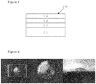
- the surface treated metal material 10 for burn-in test socket includes a base material 11, an lower layer 12 formed on the base material 11, an intermediate layer 13 formed on the lower layer 12 and an upper layer 14 formed on the intermediate layer 13.
- base material 11 examples include, without being particularly limited to, metal base materials such as copper and copper alloys, Fe-based materials, stainless steel, titanium and titanium alloys and aluminum and aluminum alloys.
- the upper layer 14 is constituted with an alloy composed of one or two selected from the constituent element group B consisting of Sn and In and one or two or more selected from a constituent element group C consisting of Ag, Au, Pt, Pd, Ru, Rh, Os and Ir.
- Sn and In are oxidizable metals, but are characterized by being relatively soft among metals. Accordingly, even when an oxide film is formed on the surface of Sn or In, for example at the time of joining together terminals by using the surface treated metal material as a contact material, the oxide film is easily scraped to result in contact between metals, and hence a low contact resistance is obtained.
- Sn and In are excellent in the gas corrosion resistance against the gases such as chlorine gas, sulfurous acid gas and hydrogen sulfide gas; for example, when Ag poor in gas corrosion resistance is used for the upper layer 14, Ni poor in gas corrosion resistance is used for the lower layer 12, and copper or a copper alloy poor in gas corrosion resistance is used for the base material 11, Sn and In have an effect to improve the gas corrosion resistance of the surface treated metal material.
- Sn and In Sn is preferable because In is severely regulated on the basis of the technical guidelines for the prevention of health impairment prescribed by the Ordinance of Ministry of Health, Labour and Welfare.
- Ag, Au, Pt, Pd, Ru, Rh, Os and Ir are characterized by being relatively heat-resistant among metals. Accordingly, these metals suppress the diffusion of the composition of the base material 11, the lower layer 12 and the intermediate layer 13 toward the side of the upper layer 14 to improve the heat resistance. These metals also form compounds with Sn or In in the upper layer 14 to suppress the formation of the oxide film of Sn or In, so as to improve the solder wettability.
- Ag Au, Pt, Pd, Ru, Rh, Os and Ir
- Ag is more desirable from the viewpoint of electrical conductivity. Ag is high in electrical conductivity. For example, when Ag is used for highfrequency wave signals, impedance resistance is made low due to the skin effect.
- the thickness of the upper layer 14 is required to be 0.02 ⁇ m or more and less than 1.00 ⁇ m.
- the thickness of the upper layer 14 is less than 0.02 ⁇ m, the composition of the base material 11 or the lower layer 12 tends to diffuse to the side of the upper layer 14 and the heat resistance or the solder wettability is degraded.
- the upper layer is worn by fine sliding, and the lower layer 12 high in contact resistance tends to be exposed, and hence the fine sliding wear resistance is poor and the contact resistance tends to be increased by fine sliding.
- the lower layer 12 poor in gas corrosion resistance tends to be exposed, and hence the gas corrosion resistance is poor, and the exterior appearance is discolored when a gas corrosion test is performed.
- the thickness of the upper layer 14 is 1.00 ⁇ m or more, the thin film lubrication effect due to the hard base material 11 or the hard lower layer 12 is degraded and the adhesive wear is increased. The mechanical durability is also degraded and scraping of plating tends to occur.
- the upper layer 14 preferably includes the metal(s) of the constituent element group B in a content of 10 to 50 at%.
- the content of the metal(s) of the constituent element group B is less than 10 at%, for example, in the case where the metal of the constituent element group C is Ag, the gas corrosion resistance is poor, and the exterior appearance can be discolored when a gas corrosion test is performed.
- the content of the metal(s) of the constituent element group B exceeds 50 at%, the proportion of the metal(s) of the constituent element group B in the upper layer 14 is large and the adhesive wear can be increased.
- the intermediate layer 13 constituted with one or two or more selected from the constituent element group A consisting of Ni, Cr, Mn, Fe, Co and Cu, and one or two selected from the constituent element group B consisting of Sn and In is required to be formed in a thickness of 0.01 ⁇ m or more and less than 0.40 ⁇ m.
- Sn and In are excellent in the gas corrosion resistance against the gases such as chlorine gas, sulfurous acid gas and hydrogen sulfide gas, for example, when Ni poor in gas corrosion resistance is used for the lower layer 12 and copper and copper alloy poor in gas corrosion resistance is used for the base material 11, Sn and In have a function to improve the gas corrosion resistance of the surface treated metal material.
- Ni, Cr, Mn, Fe, Co and Cu provide a harder coating as compared with Sn and In, accordingly make the adhesive wear hardly occur, prevent the diffusion of the constituent metal(s) of the base material 11 into the upper layer 14, and thus improve the durability in such a way that the degradation of the heat resistance or the degradation of the solder wettability is suppressed.
- the thickness of the intermediate layer 13 is less than 0.01 ⁇ m, the coating becomes soft and the adhesive wear is increased.
- the thickness of the intermediate layer 13 is 0.40 ⁇ m or more, the bending processability is degraded, the mechanical durability is also degraded, and scraping of plating can occur.
- Sn is preferable because In is severely regulated on the basis of the technical guidelines for the prevention of health impairment prescribed by the Ordinance of Ministry of Health, Labour and Welfare.
- Ni is preferable among Ni, Cr, Mn, Fe, Co and Cu. This is because Ni is hard, and accordingly the adhesive wear hardly occurs and sufficient bending processability is obtained.
- the content of the metal(s) of the constituent element group B is preferably 35 at% or more.
- the content of Sn is 35 at% or more, the coating becomes hard and the adhesive wear can be decreased.
- the lower layer 12 constituted with one or two or more selected from the constituent element group A consisting of Ni, Cr, Mn, Fe, Co and Cu.
- the hard lower layer 12 is formed, hence the thin film lubrication effect is improved and the adhesive wear is decreased, and the lower layer 12 prevents the diffusion of the constituent metal(s) of the base material 11 into the upper layer 14 and improves, for example, the heat resistance or the solder wettability.
- the thickness of the lower layer 12 is required to be 0.05 ⁇ m or more.
- the thickness of the lower layer 12 is less than 0.05 ⁇ m, the thin film lubrication effect due to the hard lower layer is degraded and the adhesive wear is increased. The diffusion of the constituent metal(s) of the base material 11 into the upper layer 14 is facilitated, and the heat resistance or the solder wettability is degraded.
- the thickness of the lower layer 12 is required to be less than 5.00 ⁇ m. When the thickness is 5.00 ⁇ m or more, bending processability is poor.
- a layer constituted with an alloy of the metal(s) of the constituent element group A and the metal(s) of the constituent element group C may also be provided.
- a Ni-Ag alloy layer is preferable.
- the constituent element group A can comprise the metal(s) consisting of the group of Ni, Cr, Mn, Fe, Co and Cu in a total content of 50 mass% or more and further comprise metal(s) of one or two or more selected from the group consisting of B, P, Sn and Zn.
- the alloy composition of the lower layer 12 having such a constitution as described above makes the lower layer 12 harder and further improves the thin film lubrication effect to further decrease the adhesive wear, the alloying of the lower layer 12 further prevents the diffusion of the constituent metals of the base material 11 into the upper layer, and can improve the durability such as the heat resistance and the solder wettability.
- the constituent element group B can comprise the metal(s) consisting of the group of Sn and In in a total content of 50 mass% or more and further comprise metal(s) of one or two or more selected from the group consisting of Ag, As, Au, Bi, Cd, Co, Cr, Cu, Fe, Mn, Mo, Ni, Pb, Sb, W and Zn. These metals can decrease the adhesive wear, suppress the occurrence of whisker, and additionally improve the durability such as the heat resistance or the solder wettability.
- the constituent element group C can comprise the metal(s) consisting of the group of Ag, Au, Pt, Pd, Ru, Rh, Os and Ir in a total content of 50 mass% or more and further comprise metal(s) of one or two or more selected from the group consisting of Bi,Cd, Co, Cu, Fe, In, Mn, Mo, Ni, Pb, Sb, Se, Sn, W, Tl and Zn.
- These metals further can decrease the adhesive wear, suppresse the occurrence of whisker, and additionally improve the durability such as the heat resistance or the solder wettability.
- a contact resistance value of the surface treated metal material for burn-in test socket of the present invention is 2.0 m ⁇ or less when held for 200 hours at 180°C with contacting the surface treated metal material with other metal material(s) from a side of the upper layer. Accordingly, the surface treated metal material for burn-in test socket of the present invention, when used in the connector for burn-in test socket, can excellently suppress increase of contact resistance even when heated and held under predetermined conditions in contact with another metal material.
- the contact resistance value is preferably 1.8 m ⁇ or less, more preferably 1.6 m ⁇ or less.
- a diffusion depth of a coating metal element of the other metal material(s) in the surface treated metal material for burn-in test socket of the present invention when held for 200 hours at 180°C with contacting the surface treated metal material at contact load of 2.4 N with other metal material(s) from the side of the upper layer, is 0.5 ⁇ m or less from the surface of the surface treated metal material. Accordingly, the surface treated metal material for burn-in test socket of the present invention, when used in the connector for burn-in test socket, can excellently suppress increase of contact resistance even when heated, held and applied a load under predetermined conditions in contact with another metal material.
- the diffusion depth of the coating metal element of the other metal material(s) in the surface treated metal material is preferably 0.4 ⁇ m or less from the surface of the surface treated metal material, and more preferably 0.3 ⁇ m or less from the surface of the surface treated metal material.
- the surface treated metal material for burn-in test socket of the present invention can be used as a connector for burn-in test socket.
- a burn-in test socket can be produced by using the connector manufactured by using the surface treated metal material for burn-in test socket of the present invention.
- the burn-in test socket comprising the connector manufactured by using the surface treated metal material for burn-in test socket of the present invention, a contact resistance between a contact of the burn-in test socket and other metal material(s) can be excellently suppressed.
- the method for producing the surface treated metal material for burn-in test socket of the present invention for example, either a wet plating (electroplating or electroless plating) or a dry plating (sputtering or ion plating) can be used.
- Example 1 to 16 Comparative Examples 1 to 5, 8, 9, and Reference Examples 6, 7, under the following conditions, the surface treatment was performed in the sequence of electrolytic first plating, second plating, and/or third plating, and phosphate ester type liquid treatment and heat treatment on the surface of the base material (dome material).
- Table 1 shows plating type, plating thickness at manufacturing, conditions of phosphate ester type liquid treatment and heat treatment in Examples, Comparative Examples, Reference Examples.
- phosphate ester type liquid treatment was conducted on the surface of the plating, under the following conditions by using the following phosphate ester species (A1, A2) and cyclic organic compound species (B1, B2), as shown Table 1. Deposition amounts of P and N on the surface of the plating after phosphate ester type liquid treatment are shown in Table 1.
- the surface treatment can be conducted by coating phosphate ester type liquid on the surface of the manufactured upper layer 14.
- An example of the coating method can be spray coating, flow coating, dip coating, roll coating and so on.
- the dip coating and the spray coating are preferable from the viewpoint of productivity.
- the treatment method can be conducted by immersing the metal material after manufacturing the upper layer 14 in the phosphate ester type liquid to conduct electrolysis by using the metal material as anode.
- the metal material treated with the method has advantages that contact resistance under high temperature environment is harder to rise.
- the surface treatment by phosphate ester type liquid can be conducted after the upper layer 14 is manufactured or after reflow processing to the manufactured upper layer 14. There is no time restriction for the surface treatment, but it is preferable to be conducted in a series of steps from an industrial point of view.
- the thickness of the lower layer was measured with the X-ray fluorescent analysis thickness meter (SEA5100, collimator: 0.1 mm ⁇ , manufactured by Seiko Instruments Inc.).
- the determination of the structures and the measurement of the thicknesses of the upper layer and the intermediate layer of each of the obtained samples were performed by the line analysis based on the STEM (scanning transmission electron microscope) analysis.
- the thickness corresponds to the distance determined from the line analysis (or area analysis).
- the STEM apparatus the JEM-2100F manufactured by JEOL Ltd. was used.
- the acceleration voltage of this apparatus is 200 kV.
- the evaluations were performed for arbitrary 10 points and the resulting values were averaged.
- the thickness of the surface layer was measured in the same way as the upper layer and the intermediate layer.
- Figure 2 shows an observed picture of sample showing a state of contact resistance evaluation.
- a left figure shows overall plane observation picture of dome material
- a central figure shows enlarged plane observation picture of dome material
- a right figure shows side plane observation picture of dome material.
- the manufactured plate material was inserted into the dome material to contact with. Next, in maintaining the sate of contacting the plate material with the dome material, they were held for 200 hours at 180 °C. Then, the contact resistance was measured with the contact simulator model CRS-113-Au manufactured by Yamasaki-seiki Co., Ltd., under the condition of the contact load of 1N, 2N, 3N and 5N, on the basis of the four-terminal method.
- the manufactured plate material was inserted into the dome material to contact with at contact load of 2.4 N.
- they were held for 200 hours at 180 °C.
- Tables 1 and 2 Composition, evaluation conditions and results of each sample are shown in Tables 1 and 2.
- Thiickness indicates the thickness of first plating, second plating and third plating to produce.
- Thiickness indicates the thickness of alloyed plating.
- Example 16 Plating species Thickness [ ⁇ m] Plating species Thickness [ ⁇ m] Plating species Thickness [ ⁇ m] Phosphate ester species Cyclic organic compound species Deposition amounts of P mol/cm2 Deposition amounts of N mol/cm2 Temperature [°C] Time [sec] Atmosphere
- Example 2 Ni-Co 1.0 Ag 0.2 Sn 0.15 A1 B1 7 ⁇ 10 -6 2 ⁇ 10 -6 650 10 N 2 gas
- Example 3 Ni 1.0 Ag- Sn 0.2 Sn 0.15 A1 B1 7 ⁇ 10 -6 2 ⁇ 10 -6 650 10 N 2 gas
- Example 4 Ni 1.0 Ag 0.2 Sn 0.15 A1 B1 8 ⁇ 10 -6 3 ⁇ 10 -6 650 12 N 2 gas
- Example 5 Ni 1.0 Ag 0.2 Sn- Ag 0.15 A
- the contact resistance value was 2.0 m ⁇ or less by being held for 200 hours at 180°C with contacting the dome material with the plate material, and the contact resistance can be excellently suppressed.
- the contact resistance value is the same level as Reference Example 6 in which the upper layer constituted with Ag layer of the thickness of 2 ⁇ m including the change over time, and Reference Example 7 in which the upper layer constituted with Au layer of the thickness of 0.4 ⁇ m.
Landscapes
- Chemical & Material Sciences (AREA)
- Engineering & Computer Science (AREA)
- Materials Engineering (AREA)
- Metallurgy (AREA)
- Organic Chemistry (AREA)
- General Physics & Mathematics (AREA)
- Physics & Mathematics (AREA)
- Chemical Kinetics & Catalysis (AREA)
- Mechanical Engineering (AREA)
- Electrochemistry (AREA)
- Computer Hardware Design (AREA)
- Microelectronics & Electronic Packaging (AREA)
- General Engineering & Computer Science (AREA)
- Environmental & Geological Engineering (AREA)
- Electroplating Methods And Accessories (AREA)
- Contacts (AREA)
Abstract
Description
- The present invention relates to a surface treated metal material for burn-in test socket, a connector for burn-in test socket and a burn-in test socket using the same.
- In a quality test conducted to remove in advance initial failure of semiconductor devices and so on, a burn-in test is conducted to reduce testing time by heating a specimen with temperature and voltage controls to accelerate degradation of the specimen.
- A burn-in test socket is used for the burn-in test (Patent Literature 1), and comprises a connector for burn-in test socket in an electrical contact portion with the specimen.
- [Patent Literature 1] Japanese Patent Application Laid-Open Publication No.
2010-109386 - A contact resistance value of the contact used for burn-in test socket can increase when a heat retention test at a predetermined temperature and for a predetermined time is conducted by contacted with a metal material of the specimen. When the contact resistance value increases, it is difficult to conduct burn-in test accurately because there is a risk of erroneously determining that the resistance value of IC being tested rises.
- The present invention has been made to solve the above problems, and provides a surface treated metal material for burn-in test socket wherein contact resistance between the contact of the socket and other metal materials being inserted is excellently suppressed when used for the contact for burn-in test socket.
- The present inventors made a diligent study, and consequently have discovered that a surface treated metal material for burn-in test socket to solve the problem can be prepared by disposing a lower layer, an intermediate layer and an upper layer in this order on a base material, using predetermined metals for the lower layer, the intermediate layer and the upper layer, respectively, and assigning predetermined thickness values and predetermined compositions to the lower, intermediate and upper layers, respectively.
- An aspect of the present invention perfected on the basis of the above-described discovery is a surface treated metal material for burn-in test socket, comprising
a base material,
a lower layer being constituted with one or two or more selected from the constituent element group A, the constituent element group A consisting of Ni, Cr, Mn, Fe, Co and Cu,
an intermediate layer formed on the lower layer, the intermediate layer being constituted with one or two or more selected from the constituent element group A and one or two selected from a constituent element group B, the constituent element group B consisting of Sn and In, and
an upper layer formed on the intermediate layer, the upper layer being constituted with one or two selected from the constituent element group B and one or two or more selected from a constituent element group C, the constituent element group C consisting of Ag, Au, Pt, Pd, Ru, Rh, Os and Ir, wherein
the thickness of the lower layer is 0.05 µm or more and less than 5.00 µm, the thickness of the intermediate layer is 0.01 µm or more and less than 0.40 µm, and the thickness of the upper layer is 0.02 µm or more and less than 1.00 µm. - In the surface treated metal material for burn-in test socket of the present invention in an embodiment, the surface treated metal material has a contact resistance value of 2.0 mΩ or less by being held for 200 hours at 180°C with contacting the surface treated metal material with other metal material(s) from a side of the upper layer.
- In the surface treated metal material for burn-in test socket of the present invention in another embodiment, a diffusion depth of a coating metal element of the other metal material(s) in the surface treated metal material, by being held for 200 hours at 180°C with contacting the surface treated metal material at contact load of 2.4 N with other metal material(s) from a side of the upper layer, is 0.5 µm or less from a surface of the surface treated metal material.
- In the surface treated metal material for burn-in test socket of the present invention in yet another embodiment, the upper layer comprises the metal(s) of the constituent element group B in a content of 10 to 50 at%.
- In the surface treated metal material for burn-in test socket of the present invention in yet another embodiment, the intermediate layer comprises the metal(s) of the constituent element group B in a content of 35 at% or more.
- In the surface treated metal material for burn-in test socket of the present invention in yet another embodiment, the constituent element group A comprises the metal(s) consisting of the group of Ni, Cr, Mn, Fe, Co and Cu in a total content of 50 mass% or more and further comprises metal(s) of one or two or more selected from the group consisting of B, P, Sn and Zn.
- In the surface treated metal material for burn-in test socket of the present invention in yet another embodiment, the constituent element group B comprises the metal(s) consisting of the group of Sn and In in a total content of 50 mass% or more and further comprises metal(s) of one or two or more selected from the group consisting of Ag, As, Au, Bi, Cd, Co, Cr, Cu, Fe, Mn, Mo, Ni, Pb, Sb, W and Zn.
- In the surface treated metal material for burn-in test socket of the present invention in yet another embodiment, the constituent element group C comprises the metal(s) consisting of the group of Ag, Au, Pt, Pd, Ru, Rh, Os and Ir in a total content of 50 mass% or more and further comprises metal(s) of one or two or more selected from the group consisting of Bi,Cd, Co, Cu, Fe, In, Mn, Mo, Ni, Pb, Sb, Se, Sn, W, Tl and Zn.
- In the surface treated metal material for burn-in test socket of the present invention in yet another embodiment, the surface treated metal material further comprises a layer between the lower layer and the intermediate layer, being constituted with an alloy of the metal(s) in the constituent element group A and the metal(s) in the constituent element group C.
- The present invention is, in another aspect thereof, a connector for burn-in test socket comprising the surface treated metal material of the present invention.
- The present invention is, in yet another aspect thereof, a burn-in test socket comprising the connector of the present invention.
- According to the present invention, it is possible to provide a surface treated metal material for burn-in test socket wherein contact resistance between the contact of the socket and other metal materials being inserted is excellently suppressed when used for the contact for burn-in test socket.
-
- [
Figure 1] Figure 1 is a schematic diagram illustrating the structure of a surface treated metal material according to an embodiment of the present invention. - [
Figure 2] Figure 2 is an observed picture of sample showing a state of contact resistance evaluation. - Hereinafter, the surface treated metal material for burn-in test socket according to the embodiments of the present invention are described. As shown in
Figure 1 , the surface treatedmetal material 10 for burn-in test socket according to an embodiment includes a base material 11, an lower layer 12 formed on the base material 11, an intermediate layer 13 formed on the lower layer 12 and anupper layer 14 formed on the intermediate layer 13. - Usable examples of the base material 11 include, without being particularly limited to, metal base materials such as copper and copper alloys, Fe-based materials, stainless steel, titanium and titanium alloys and aluminum and aluminum alloys.
- The
upper layer 14 is constituted with an alloy composed of one or two selected from the constituent element group B consisting of Sn and In and one or two or more selected from a constituent element group C consisting of Ag, Au, Pt, Pd, Ru, Rh, Os and Ir. - Sn and In are oxidizable metals, but are characterized by being relatively soft among metals. Accordingly, even when an oxide film is formed on the surface of Sn or In, for example at the time of joining together terminals by using the surface treated metal material as a contact material, the oxide film is easily scraped to result in contact between metals, and hence a low contact resistance is obtained.
- Sn and In are excellent in the gas corrosion resistance against the gases such as chlorine gas, sulfurous acid gas and hydrogen sulfide gas; for example, when Ag poor in gas corrosion resistance is used for the
upper layer 14, Ni poor in gas corrosion resistance is used for the lower layer 12, and copper or a copper alloy poor in gas corrosion resistance is used for the base material 11, Sn and In have an effect to improve the gas corrosion resistance of the surface treated metal material. As for Sn and In, Sn is preferable because In is severely regulated on the basis of the technical guidelines for the prevention of health impairment prescribed by the Ordinance of Ministry of Health, Labour and Welfare. - Ag, Au, Pt, Pd, Ru, Rh, Os and Ir are characterized by being relatively heat-resistant among metals. Accordingly, these metals suppress the diffusion of the composition of the base material 11, the lower layer 12 and the intermediate layer 13 toward the side of the
upper layer 14 to improve the heat resistance. These metals also form compounds with Sn or In in theupper layer 14 to suppress the formation of the oxide film of Sn or In, so as to improve the solder wettability. Among Ag, Au, Pt, Pd, Ru, Rh, Os and Ir, Ag is more desirable from the viewpoint of electrical conductivity. Ag is high in electrical conductivity. For example, when Ag is used for highfrequency wave signals, impedance resistance is made low due to the skin effect. - The thickness of the
upper layer 14 is required to be 0.02 µm or more and less than 1.00 µm. When the thickness of theupper layer 14 is less than 0.02 µm, the composition of the base material 11 or the lower layer 12 tends to diffuse to the side of theupper layer 14 and the heat resistance or the solder wettability is degraded. Additionally, the upper layer is worn by fine sliding, and the lower layer 12 high in contact resistance tends to be exposed, and hence the fine sliding wear resistance is poor and the contact resistance tends to be increased by fine sliding. Moreover, the lower layer 12 poor in gas corrosion resistance tends to be exposed, and hence the gas corrosion resistance is poor, and the exterior appearance is discolored when a gas corrosion test is performed. On the other hand, when the thickness of theupper layer 14 is 1.00 µm or more, the thin film lubrication effect due to the hard base material 11 or the hard lower layer 12 is degraded and the adhesive wear is increased. The mechanical durability is also degraded and scraping of plating tends to occur. - The
upper layer 14 preferably includes the metal(s) of the constituent element group B in a content of 10 to 50 at%. When the content of the metal(s) of the constituent element group B is less than 10 at%, for example, in the case where the metal of the constituent element group C is Ag, the gas corrosion resistance is poor, and the exterior appearance can be discolored when a gas corrosion test is performed. On the other hand, when the content of the metal(s) of the constituent element group B exceeds 50 at%, the proportion of the metal(s) of the constituent element group B in theupper layer 14 is large and the adhesive wear can be increased. - Between the lower layer 12 and the
upper layer 14, the intermediate layer 13 constituted with one or two or more selected from the constituent element group A consisting of Ni, Cr, Mn, Fe, Co and Cu, and one or two selected from the constituent element group B consisting of Sn and In is required to be formed in a thickness of 0.01 µm or more and less than 0.40 µm. Sn and In are excellent in the gas corrosion resistance against the gases such as chlorine gas, sulfurous acid gas and hydrogen sulfide gas, for example, when Ni poor in gas corrosion resistance is used for the lower layer 12 and copper and copper alloy poor in gas corrosion resistance is used for the base material 11, Sn and In have a function to improve the gas corrosion resistance of the surface treated metal material. Ni, Cr, Mn, Fe, Co and Cu provide a harder coating as compared with Sn and In, accordingly make the adhesive wear hardly occur, prevent the diffusion of the constituent metal(s) of the base material 11 into theupper layer 14, and thus improve the durability in such a way that the degradation of the heat resistance or the degradation of the solder wettability is suppressed. - When the thickness of the intermediate layer 13 is less than 0.01 µm, the coating becomes soft and the adhesive wear is increased. On the other hand, the thickness of the intermediate layer 13 is 0.40 µm or more, the bending processability is degraded, the mechanical durability is also degraded, and scraping of plating can occur.
- Of Sn and In, Sn is preferable because In is severely regulated on the basis of the technical guidelines for the prevention of health impairment prescribed by the Ordinance of Ministry of Health, Labour and Welfare. Ni is preferable among Ni, Cr, Mn, Fe, Co and Cu. This is because Ni is hard, and accordingly the adhesive wear hardly occurs and sufficient bending processability is obtained.
- In the intermediate layer 13, the content of the metal(s) of the constituent element group B is preferably 35 at% or more. When the content of Sn is 35 at% or more, the coating becomes hard and the adhesive wear can be decreased.
- Between the base material 11 and the intermediate layer 13, it is necessary to form the lower layer 12 constituted with one or two or more selected from the constituent element group A consisting of Ni, Cr, Mn, Fe, Co and Cu. By forming the lower layer 12 with one or two or more metals selected from the constituent element group A consisting of Ni, Cr, Mn, Fe, Co and Cu, the hard lower layer 12 is formed, hence the thin film lubrication effect is improved and the adhesive wear is decreased, and the lower layer 12 prevents the diffusion of the constituent metal(s) of the base material 11 into the
upper layer 14 and improves, for example, the heat resistance or the solder wettability. - The thickness of the lower layer 12 is required to be 0.05 µm or more. When the thickness of the lower layer 12 is less than 0.05 µm, the thin film lubrication effect due to the hard lower layer is degraded and the adhesive wear is increased. The diffusion of the constituent metal(s) of the base material 11 into the
upper layer 14 is facilitated, and the heat resistance or the solder wettability is degraded. On the other hand, the thickness of the lower layer 12 is required to be less than 5.00 µm. When the thickness is 5.00 µm or more, bending processability is poor. - Between the lower layer 12 and the intermediate layer 13, a layer constituted with an alloy of the metal(s) of the constituent element group A and the metal(s) of the constituent element group C may also be provided. As the layer concerned, for example, a Ni-Ag alloy layer is preferable. When such a layer is formed between the lower layer 12 and the intermediate layer 13, the diffusion of the constituent metal(s) of the base material 11 into the
upper layer 14 is further satisfactorily prevented, and for example, the heat resistance or the solder wettability is improved. - The constituent element group A can comprise the metal(s) consisting of the group of Ni, Cr, Mn, Fe, Co and Cu in a total content of 50 mass% or more and further comprise metal(s) of one or two or more selected from the group consisting of B, P, Sn and Zn. The alloy composition of the lower layer 12 having such a constitution as described above makes the lower layer 12 harder and further improves the thin film lubrication effect to further decrease the adhesive wear, the alloying of the lower layer 12 further prevents the diffusion of the constituent metals of the base material 11 into the upper layer, and can improve the durability such as the heat resistance and the solder wettability.
- The constituent element group B can comprise the metal(s) consisting of the group of Sn and In in a total content of 50 mass% or more and further comprise metal(s) of one or two or more selected from the group consisting of Ag, As, Au, Bi, Cd, Co, Cr, Cu, Fe, Mn, Mo, Ni, Pb, Sb, W and Zn. These metals can decrease the adhesive wear, suppress the occurrence of whisker, and additionally improve the durability such as the heat resistance or the solder wettability.
- The constituent element group C can comprise the metal(s) consisting of the group of Ag, Au, Pt, Pd, Ru, Rh, Os and Ir in a total content of 50 mass% or more and further comprise metal(s) of one or two or more selected from the group consisting of Bi,Cd, Co, Cu, Fe, In, Mn, Mo, Ni, Pb, Sb, Se, Sn, W, Tl and Zn. These metals further can decrease the adhesive wear, suppresse the occurrence of whisker, and additionally improve the durability such as the heat resistance or the solder wettability.
- A contact resistance value of the surface treated metal material for burn-in test socket of the present invention is 2.0 mΩ or less when held for 200 hours at 180°C with contacting the surface treated metal material with other metal material(s) from a side of the upper layer. Accordingly, the surface treated metal material for burn-in test socket of the present invention, when used in the connector for burn-in test socket, can excellently suppress increase of contact resistance even when heated and held under predetermined conditions in contact with another metal material. The contact resistance value is preferably 1.8 mΩ or less, more preferably 1.6 mΩ or less.
- Furthermore, a diffusion depth of a coating metal element of the other metal material(s) in the surface treated metal material for burn-in test socket of the present invention, when held for 200 hours at 180°C with contacting the surface treated metal material at contact load of 2.4 N with other metal material(s) from the side of the upper layer, is 0.5 µm or less from the surface of the surface treated metal material. Accordingly, the surface treated metal material for burn-in test socket of the present invention, when used in the connector for burn-in test socket, can excellently suppress increase of contact resistance even when heated, held and applied a load under predetermined conditions in contact with another metal material. The diffusion depth of the coating metal element of the other metal material(s) in the surface treated metal material is preferably 0.4 µm or less from the surface of the surface treated metal material, and more preferably 0.3 µm or less from the surface of the surface treated metal material.
- The surface treated metal material for burn-in test socket of the present invention can be used as a connector for burn-in test socket. A burn-in test socket can be produced by using the connector manufactured by using the surface treated metal material for burn-in test socket of the present invention. In the burn-in test socket comprising the connector manufactured by using the surface treated metal material for burn-in test socket of the present invention, a contact resistance between a contact of the burn-in test socket and other metal material(s) can be excellently suppressed.
- As the method for producing the surface treated metal material for burn-in test socket of the present invention, for example, either a wet plating (electroplating or electroless plating) or a dry plating (sputtering or ion plating) can be used.
- Hereinafter, both Examples of the present invention and Comparative Examples are presented, these Examples and Comparative Examples are provided for better understanding of the present invention, and are not intended to limit the present invention.
- As materials, the following plate material and dome material was prepared.
- As Examples 1 to 16, Comparative Examples 1 to 5, 8, 9, and Reference Examples 6, 7, under the following conditions, the surface treatment was performed in the sequence of electrolytic first plating, second plating, and/or third plating, and phosphate ester type liquid treatment and heat treatment on the surface of the base material (dome material). Table 1 shows plating type, plating thickness at manufacturing, conditions of phosphate ester type liquid treatment and heat treatment in Examples, Comparative Examples, Reference Examples.
-
- (1) "Plate material" thickness: 0.25 mm, width: 8 mm, component: brass, Sn plating of the thickness of 1.0 µm
- (2) "Dome material" thickness: 0.2 mm, width: 12 mm, component: brass
- (First Plating Conditions)
- [Ni plating]
- Surface treatment method: Electroplating
- Plating solution: Ni sulfamate (150 g/L) + boric acid (30 g/L)
- Plating temperature: 55 °C
- Electric current density: 0.5 to 4 A/dm2
- [Ni-Co plating]
- Surface treatment method: Electroplating
- Plating solution: Ni sulfamate (60 g/L) + cobalt sulfate (60 g/L) + boric acid (30 g/L)
- Plating temperature: 55 °C
- Electric current density: 0.5 to 4 A/dm2
- [Ni plating]
- (Second Plating Conditions)
- [Ag plating]
- Surface treatment method: Electroplating
- Plating solution: Ag cyanide (10 g/L) + potassium cyanide (30 g/L)
- Plating temperature: 40 °C
- Electric current density: 0.2 to 4 A/dm2
- [Ag-Sn plating]
- Surface treatment method: Electroplating
- Plating solution: Ag methanesulfonate (1 g/L) + Sn methanesulfonate (50 g/L) + methanesulfonic acid (180 g/L)
- Plating temperature: 25 °C
- Electric current density: 3 to 5 A/dm2
- [Sn plating]
- Surface treatment method: Electroplating
- Plating solution: Sn methanesulfonate (50 g/L) + methanesulfonic acid (200 g/L)
- Plating temperature: 30 °C
- Electric current density: 5 to 7 A/dm2
- [In plating]
- Surface treatment method: Electroplating
- Plating solution: In methanesulfonate (50 g/L) + methanesulfonic acid (200 g/L)
- Plating temperature: 40 °C
- Electric current density: 5 to 7 A/dm2
- [Ag plating]
- (Third Plating Conditions)
- [Sn plating]
- Surface treatment method: Electroplating
- Plating solution: Sn methanesulfonate (50 g/L) + methanesulfonic acid (200 g/L)
- Plating temperature: 30 °C
- Electric current density: 5 to 7 A/dm2
- [Sn-Ag plating]
- Surface treatment method: Electroplating
- Plating solution: Ag methanesulfonate (1 g/L) + Sn methanesulfonate (50 g/L) + methanesulfonic acid (180 g/L)
- Plating temperature: 25 °C
- Electric current density: 3 to 5 A/dm2
- [Sn plating]
- After forming first plating, second plating and third plating, phosphate ester type liquid treatment was conducted on the surface of the plating, under the following conditions by using the following phosphate ester species (A1, A2) and cyclic organic compound species (B1, B2), as shown Table 1. Deposition amounts of P and N on the surface of the plating after phosphate ester type liquid treatment are shown in Table 1.
[Phosphate ester species: A1]
Lauryl acid phosphate monoester (phosphoric acid monolauryl ester)
[Phosphate ester species: A2]
Lauryl acid phosphate diester (phosphoric acid dilauryl ester)
[Cyclic organic compound species: B1]
Benzotriazole
[Cyclic organic compound species: B2]
Sodium salt of mercaptobenzothiazole - The surface treatment can be conducted by coating phosphate ester type liquid on the surface of the manufactured
upper layer 14. An example of the coating method can be spray coating, flow coating, dip coating, roll coating and so on. The dip coating and the spray coating are preferable from the viewpoint of productivity. On the other hand, as the other example, the treatment method can be conducted by immersing the metal material after manufacturing theupper layer 14 in the phosphate ester type liquid to conduct electrolysis by using the metal material as anode. The metal material treated with the method has advantages that contact resistance under high temperature environment is harder to rise. - The surface treatment by phosphate ester type liquid, as explained so far, can be conducted after the
upper layer 14 is manufactured or after reflow processing to the manufacturedupper layer 14. There is no time restriction for the surface treatment, but it is preferable to be conducted in a series of steps from an industrial point of view. - Finally, the heat treatment was performed, under the atmosphere and the heating time shown in Table 1, by placing the sample on a hot plate, and verifying that the surface of the hot plate reached the temperature shown in Table 1.
- The thickness of the lower layer was measured with the X-ray fluorescent analysis thickness meter (SEA5100, collimator: 0.1 mmΦ, manufactured by Seiko Instruments Inc.).
- In the measurement of the thickness of the lower layer, the evaluations were performed for arbitrary 10 points and the resulting values were averaged.
- The determination of the structures and the measurement of the thicknesses of the upper layer and the intermediate layer of each of the obtained samples were performed by the line analysis based on the STEM (scanning transmission electron microscope) analysis. The thickness corresponds to the distance determined from the line analysis (or area analysis). As the STEM apparatus, the JEM-2100F manufactured by JEOL Ltd. was used. The acceleration voltage of this apparatus is 200 kV.
- In the determination of the structures and measurement of the thicknesses of the upper layer and the intermediate layer of each of the obtained samples, the evaluations were performed for arbitrary 10 points and the resulting values were averaged. The thickness of the surface layer was measured in the same way as the upper layer and the intermediate layer.
- A contact resistance evaluation of each sample was conducted under the following conditions.
Figure 2 shows an observed picture of sample showing a state of contact resistance evaluation. InFigure 2 , a left figure shows overall plane observation picture of dome material, a central figure shows enlarged plane observation picture of dome material and a right figure shows side plane observation picture of dome material. - As shown in
Figure 2 , the manufactured plate material was inserted into the dome material to contact with. Next, in maintaining the sate of contacting the plate material with the dome material, they were held for 200 hours at 180 °C. Then, the contact resistance was measured with the contact simulator model CRS-113-Au manufactured by Yamasaki-seiki Co., Ltd., under the condition of the contact load of 1N, 2N, 3N and 5N, on the basis of the four-terminal method. - In addition, the manufactured plate material was inserted into the dome material to contact with at contact load of 2.4 N. Next, in maintaining the sate of contacting the plate material with the dome material, they were held for 200 hours at 180 °C. Then, the depth of diffusion to the dome material, of a coating metal element of a surface of the plate material, from a surface of the dome material, was measured.
- Composition, evaluation conditions and results of each sample are shown in Tables 1 and 2. "Thickness" in Table 1 indicates the thickness of first plating, second plating and third plating to produce. "Thickness" in Table 2 indicates the thickness of alloyed plating.
[Table 1] First plating Second plating Third plating Phosphate ester type liquid treatment condition Heat treatment (Dipping treatment in non-underlined section. Anodic electrolysis at 2V for 5 seconds in underlined section. Example 16) Plating species Thickness [µm] Plating species Thickness [µm] Plating species Thickness [µm] Phosphate ester species Cyclic organic compound species Deposition amounts of P mol/cm2 Deposition amounts of N mol/cm2 Temperature [°C] Time [sec] Atmosphere Example 1 Ni 1.0 Ag 0.2 Sn 0.15 A1 B1 6 × 10⁻⁶ 2 × 10⁻⁶ 650 10 N2 gas Example 2 Ni-Co 1.0 Ag 0.2 Sn 0.15 A1 B1 7 × 10⁻⁶ 2 × 10⁻⁶ 650 10 N2 gas Example 3 Ni 1.0 Ag- Sn 0.2 Sn 0.15 A1 B1 7 × 10⁻⁶ 2 × 10⁻⁶ 650 10 N2 gas Example 4 Ni 1.0 Ag 0.2 Sn 0.15 A1 B1 8 × 10⁻⁶ 3 × 10⁻⁶ 650 12 N2 gas Example 5 Ni 1.0 Ag 0.2 Sn- Ag 0.15 A1 B1 7 × 10⁻⁶ 2 × 10⁻⁶ 650 10 N2 gas Example 6 Ni 1.0 Ag 0.2 Sn 0.15 A1 81 8 × 10⁻⁶ 2 × 10⁻⁶ 670 10 N2 gas Example 7 Ni 1.0 Ag 0.2 Sn 0.15 A2 B1 7 × 10⁻⁶ 2 × 10⁻⁶ 650 10 N2 gas Example 8 Ni 1.0 Ag 0.2 Sn 0.15 A1 B2 7 × 10⁻⁶ 3 × 10⁻⁶ 650 10 N2 gas Example 9 Ni 1.0 Ag 0.2 Sn 0.15 A1 B1 7 × 10⁻⁶ 2 × 10⁻⁶ 630 15 N2 gas Example 10 Ni 1.0 Ag 0.2 Sn 0.15 A1 B1 7 × 10⁻⁶ 2 × 10⁻⁶ 650 10 N2 gas Example 11 Ni 10 Ag 0.1 Sn 0.1 A1 B1 7 × 10⁻⁶ 2 × 10⁻⁶ 650 10 N2 gas Example 12 Ni 1.0 Ag 0.2 Sn 0.2 A1 B1 7 × 10⁻⁶ 2 × 10⁻⁶ 650 10 N2 gas Example 13 Ni 1.0 Ag 0.25 Sn 0.15 A1 B1 7 × 10⁻⁶ 2 × 10⁻⁶ 650 10 N2 gas Example 14 Ni 1.0 Ag 0.2 Sn 0.25 A1 B1 7 × 10⁻⁶ 2 × 10⁻⁶ 650 10 N2 gas Example 15 Ni 0.5 Ag 0.2 Sn 0.15 A1 B1 7 × 10⁻⁶ 2 × 10⁻⁶ 650 10 N2 gas Example 16 Ni 15 Ag 0.2 Sn 0.15 A1 B1 7 × 10⁻⁶ 2 × 10⁻⁶ 650 10 N2 gas Comparative Example 1 Ni 10 Ag 0.2 Sn 0.35 A1 B1 7 × 10⁻⁶ 2 × 10⁻⁶ 650 10 N2 gas Comparative Example 2 Ni 1.0 Ag 0.2 Sn 0.15 A1 B1 7 × 10⁻⁶ 2 × 10⁻⁶ 650 5 N2 gas Comparative Example 3 Ni 1.0 Ag 0.2 Sn 0.15 A1 B1 7 × 10⁻⁶ 2 × 10⁻⁶ 600 10 N2 gas Comparative Example 4 Ni 1.0 Ag 0.2 Sn 0.15 650 10 N2 gas Comparative Example 5 Ni 1.0 Sn 1.0 Reference Example 6 Ni 1.0 Ag 2.0 Reference Example 7 Ni 1.0 Au 0.4 Comparative Example Ni 1.0 Ag- Sn 0.4 Comparative Example 9 Ni 1.0 In 1.0 [Table 2] Lower layer Intermediate layer Upper layer Surface layer Contact resistance (after held for 200hours at 180°C) Diffusion depth of metal element from the surface of the surface treated metal material Composition Thickness [µm] Composition Thickness [µm] Composition Thickness [µm] Composition Thickness [µm] before heating [mΩ] after heating [mΩ] [µm] Example 1 Ni 1.0 Ni-Sn 0.14 Ag-Sn 0.27 - - 1.70 1.54 0.24 Example 2 Ni-Co 1.0 Ni-Sn 0.12 Ag-Sn 0.22 - - 1.74 1 71 0.28 Example 3 Ni 1.0 Ni-Sn 0.17 Ag-Sn 0.25 - - 1.83 1.78 0.28 Example 4 Ni 1.0 Ni-Sn 0.15 Ag-Sn 0.25 - - 1.77 1.63 0.25 Example 5 Ni 1.0 Ni-Sn 0.10 Ag-Sn 0.31 - - 1.74 1.59 0.24 Example 6 Ni 1.0 Ni-Sn 0.14 Ag-Sn 0.22 - - 1.80 1.62 0.26 Example 7 Ni 1.0 Ni-Sn 0.13 Ag-Sn 0.23 - - 1.75 1.55 0.23 Example 8 Ni 1.0 Ni-Sn 0.15 Ag-Sn 0.26 - - 1.70 1.53 0.21 Example 9 Ni 1.0 Ni-Sn 0.13 Ag-Sn 0.27 - - 1.68 1.52 0.23 Example 10 Ni 1.0 Ni-Sn 0.14 Ag-Sn 0.28 - - 1.65 1.48 0.21 Example 11 Ni 1.0 Ni-Sn 0.07 Ag-Sn 0.14 - - 1.89 1 79 030 Example 12 Ni 1.0 Ni-Sn 0.21 Ag-Sn 0.28 - - 1.77 1.60 0.27 Example 13 Ni 1.0 Ni-Sn 0.14 Ag-Sn 0.32 - - 1.70 1 51 0.24 Example 14 Ni 1.0 Ni-Sn 0.18 Ag-Sn 0.23 - - 1.81 1.67 0.29 Example 15 Ni 0.5 Ni-Sn 0.12 Ag-Sn 0.27 - - 1.73 1.54 0.24 Example 16 Ni 1.5 Ni-Sn 0.17 Ag-Sn 0.26 - - 1.76 1.55 0.25 Comparative Example 1 Ni 1.0 Ni-Sn 0.25 Ag-Sn 0.24 Sn 0.04 2.11 3.27 - Comparative Example 2 Ni 1.0 Ni-Sn 0.06 Ag-Sn 0.19 Sn 0.08 3.36 6.78 - Comparative Example 3 Ni 1.0 Ni-Sn 0.10 Ag-Sn 0.21 Sn 0.05 2.84 4.21 - Comparative Example 4 Ni 1.0 Ni-Sn 0.15 Ag-Sn 0.27 - - 1.42 2.12 0.43 Comparative Example 5 Ni 1.0 Sn 1.0 - - 4.35 5.27 - Reference Example 6 Ni 1.0 Ag 2.0 - - 1.32 1.31 1.14 Reference Example 7 Ni 1.0 Au 0.4 - - 1.53 1.95 1.21 Comparative Example 8 Ni 1.0 Ag-Sn 0.4 - - 5.87 2.41 0.62 Comparative Example 9 Ni 1.0 In 1.0 - - 2.88 64.60 1.42 - In each of Examples 1 to 16, the contact resistance value was 2.0 mΩ or less by being held for 200 hours at 180°C with contacting the dome material with the plate material, and the contact resistance can be excellently suppressed.
- In each of Examples 1 to 16, the contact resistance value is the same level as Reference Example 6 in which the upper layer constituted with Ag layer of the thickness of 2 µm including the change over time, and Reference Example 7 in which the upper layer constituted with Au layer of the thickness of 0.4 µm.
- In each of Comparative Examples 1 to 5, 8, 9, the contact resistance value was over 2.0 mΩ by being held for 200 hours at 180°C with contacting the dome material with the plate material, and the contact resistance was poor.
- In each of Comparative Examples 1 to 3, 5, pure Sn remains on the surface layer or the upper layer, the plate material with Sn plating has the same Sn on the surface. Therefore, the diffusion depth is not clear.
-
- 10
- surface treated metal material for burn-in test socket
- 11
- base material
- 12
- lower layer
- 13
- intermediate layer
- 14
- upper layer
Claims (11)
- A surface treated metal material for burn-in test socket, comprisinga base material,a lower layer being constituted with one or two or more selected from the constituent element group A, the constituent element group A consisting of Ni, Cr, Mn, Fe, Co and Cu,an intermediate layer formed on the lower layer, the intermediate layer being constituted with one or two or more selected from the constituent element group A and one or two selected from a constituent element group B, the constituent element group B consisting of Sn and In, andan upper layer formed on the intermediate layer, the upper layer being constituted with one or two selected from the constituent element group B and one or two or more selected from a constituent element group C, the constituent element group C consisting of Ag, Au, Pt, Pd, Ru, Rh, Os and Ir, whereinthe thickness of the lower layer is 0.05 µm or more and less than 5.00 µm, the thickness of the intermediate layer is 0.01 µm or more and less than 0.40 µm, and the thickness of the upper layer is 0.02 µm or more and less than 1.00 µm.
- The surface treated metal material for burn-in test socket according to claim 1, having a contact resistance value of 2.0 mΩ or less by being held for 200 hours at 180°C with contacting the surface treated metal material with other metal material(s) from a side of the upper layer.
- The surface treated metal material for burn-in test socket according to claim 1 or 2, wherein a diffusion depth of a coating metal element of the other metal material(s) in the surface treated metal material, by being held for 200 hours at 180°C with contacting the surface treated metal material at contact load of 2.4 N with other metal material(s) from a side of the upper layer, is 0.5 µm or less from a surface of the surface treated metal material.
- The surface treated metal material for burn-in test socket according to any one of claims 1 to 3, wherein the upper layer comprises the metal(s) of the constituent element group B in a content of 10 to 50 at%.
- The surface treated metal material for burn-in test socket according to any one of claims 1 to 4, wherein the intermediate layer comprises the metal(s) of the constituent element group B in a content of 35 at% or more.
- The surface treated metal material for burn-in test socket according to any one of claims 1 to 5, wherein the constituent element group A comprises the metal(s) consisting of the group of Ni, Cr, Mn, Fe, Co and Cu in a total content of 50 mass% or more and further comprises metal(s) of one or two or more selected from the group consisting of B, P, Sn and Zn.
- The surface treated metal material for burn-in test socket according to any one of claims 1 to 6, wherein the constituent element group B comprises the metal(s) consisting of the group of Sn and In in a total content of 50 mass% or more and further comprises metal(s) of one or two or more selected from the group consisting of Ag, As, Au, Bi, Cd, Co, Cr, Cu, Fe, Mn, Mo, Ni, Pb, Sb, W and Zn.
- The surface treated metal material for burn-in test socket according to any one of claims 1 to 7, wherein the constituent element group C comprises the metal(s) consisting of the group of Ag, Au, Pt, Pd, Ru, Rh, Os and Ir in a total content of 50 mass% or more and further comprises metal(s) of one or two or more selected from the group consisting of Bi,Cd, Co, Cu, Fe, In, Mn, Mo, Ni, Pb, Sb, Se, Sn, W, Tl and Zn.
- The surface treated metal material for burn-in test socket according to any one of claims 1 to 8, further comprising a layer between the lower layer and the intermediate layer, being constituted with an alloy of the metal(s) in the constituent element group A and the metal(s) in the constituent element group C.
- A connector for burn-in test socket comprising the surface treated metal material according to any one of claims 1 to 9.
- A burn-in test socket comprising the connector according to claim 10.
Applications Claiming Priority (1)
| Application Number | Priority Date | Filing Date | Title |
|---|---|---|---|
| JP2018016777A JP6653340B2 (en) | 2018-02-01 | 2018-02-01 | Surface-treated metal material for burn-in test socket, burn-in test socket connector and burn-in test socket using the same |
Publications (3)
| Publication Number | Publication Date |
|---|---|
| EP3521014A2 true EP3521014A2 (en) | 2019-08-07 |
| EP3521014A3 EP3521014A3 (en) | 2019-10-23 |
| EP3521014B1 EP3521014B1 (en) | 2020-12-09 |
Family
ID=65268823
Family Applications (1)
| Application Number | Title | Priority Date | Filing Date |
|---|---|---|---|
| EP19154525.0A Not-in-force EP3521014B1 (en) | 2018-02-01 | 2019-01-30 | Surface treated metal material for burn-in test socket, connector for burn-in test socket and burn-in test socket using the same |
Country Status (6)
| Country | Link |
|---|---|
| US (1) | US20190234994A1 (en) |
| EP (1) | EP3521014B1 (en) |
| JP (1) | JP6653340B2 (en) |
| KR (1) | KR20190093520A (en) |
| CN (1) | CN110103584B (en) |
| TW (1) | TWI717684B (en) |
Families Citing this family (4)
| Publication number | Priority date | Publication date | Assignee | Title |
|---|---|---|---|---|
| JP7033034B2 (en) * | 2018-08-23 | 2022-03-09 | 株式会社日立製作所 | Corrosion environment monitoring method and corrosion environment monitoring system |
| WO2021188674A1 (en) * | 2020-03-18 | 2021-09-23 | Xtalic Corporation | Nanostructured palladium-based alloys and related methods |
| EP4386113A1 (en) * | 2022-12-13 | 2024-06-19 | Aptiv Technologies Limited | Electrical terminal with metal conductive layer comprising silver |
| TWI851014B (en) * | 2023-02-09 | 2024-08-01 | 朋程科技股份有限公司 | Power semiconductor packaging signal connection element and semiconductor module |
Citations (1)
| Publication number | Priority date | Publication date | Assignee | Title |
|---|---|---|---|---|
| JP2010109386A (en) | 2010-01-21 | 2010-05-13 | Renesas Technology Corp | Method of manufacturing semiconductor device, and inspection socket |
Family Cites Families (21)
| Publication number | Priority date | Publication date | Assignee | Title |
|---|---|---|---|---|
| JP2959872B2 (en) * | 1991-06-18 | 1999-10-06 | 古河電気工業株式会社 | Electrical contact material and its manufacturing method |
| JPH07220788A (en) * | 1994-01-31 | 1995-08-18 | Furukawa Electric Co Ltd:The | IC socket terminal and manufacturing method thereof |
| JP4525117B2 (en) * | 2004-03-12 | 2010-08-18 | ルネサスエレクトロニクス株式会社 | tray |
| JP4348288B2 (en) * | 2004-12-20 | 2009-10-21 | 株式会社神戸製鋼所 | Connector contact material |
| WO2007034921A1 (en) * | 2005-09-22 | 2007-03-29 | Enplas Corporation | Electrical contact and socket for electrical component |
| US7172450B1 (en) * | 2006-01-11 | 2007-02-06 | Qualitau, Inc. | High temperature open ended zero insertion force (ZIF) test socket |
| US20100139730A1 (en) * | 2006-12-04 | 2010-06-10 | Aarhus Universitet | Use of thermoelectric materials for low temperature thermoelectric purposes |
| JP5384382B2 (en) * | 2009-03-26 | 2014-01-08 | 株式会社神戸製鋼所 | Copper or copper alloy with Sn plating excellent in heat resistance and method for producing the same |
| JP5086485B1 (en) * | 2011-09-20 | 2012-11-28 | Jx日鉱日石金属株式会社 | Metal material for electronic parts and method for producing the same |
| JP5138827B1 (en) * | 2012-03-23 | 2013-02-06 | Jx日鉱日石金属株式会社 | Metal materials for electronic parts, connector terminals, connectors and electronic parts using the same |
| JP5275504B1 (en) * | 2012-06-15 | 2013-08-28 | Jx日鉱日石金属株式会社 | METAL MATERIAL FOR ELECTRONIC COMPONENT AND ITS MANUFACTURING METHOD, CONNECTOR TERMINAL USING THE SAME, CONNECTOR AND ELECTRONIC COMPONENT |
| JP5427945B2 (en) * | 2012-06-27 | 2014-02-26 | Jx日鉱日石金属株式会社 | METAL MATERIAL FOR ELECTRONIC COMPONENT AND ITS MANUFACTURING METHOD, CONNECTOR TERMINAL USING THE SAME, CONNECTOR AND ELECTRONIC COMPONENT |
| JP6029435B2 (en) * | 2012-06-27 | 2016-11-24 | Jx金属株式会社 | METAL MATERIAL FOR ELECTRONIC COMPONENT AND ITS MANUFACTURING METHOD, CONNECTOR TERMINAL USING THE SAME, CONNECTOR AND ELECTRONIC COMPONENT |
| EP2878704B1 (en) * | 2012-07-25 | 2017-08-09 | JX Nippon Mining & Metals Corporation | Metal material for electronic components, method for producing same, connector terminal using same, connector and electronic component |
| WO2014034460A1 (en) * | 2012-08-31 | 2014-03-06 | 株式会社オートネットワーク技術研究所 | Plated terminal for connector, and terminal pair |
| TWI485930B (en) * | 2012-10-04 | 2015-05-21 | Jx日鑛日石金屬股份有限公司 | Metal material for electronic parts and manufacturing method thereof |
| JP2014182976A (en) * | 2013-03-21 | 2014-09-29 | Enplas Corp | Electric contact and socket for electric component |
| JP6503159B2 (en) * | 2014-04-22 | 2019-04-17 | Jx金属株式会社 | Metal material for electronic parts, connector terminal using the same, connector and electronic parts |
| JP6219553B2 (en) * | 2015-09-01 | 2017-10-25 | 古河電気工業株式会社 | Plating material excellent in heat resistance and method for producing the same |
| CN110199054B (en) * | 2017-01-30 | 2022-02-25 | Jx金属株式会社 | Surface treatment plating material, connector terminal, connector, FFC terminal, FFC, FPC, and electronic component |
| JP6309124B1 (en) * | 2017-02-15 | 2018-04-11 | Jx金属株式会社 | METAL MATERIAL FOR ELECTRONIC COMPONENT AND ITS MANUFACTURING METHOD, CONNECTOR TERMINAL USING THE SAME, CONNECTOR AND ELECTRONIC COMPONENT |
-
2018
- 2018-02-01 JP JP2018016777A patent/JP6653340B2/en not_active Expired - Fee Related
-
2019
- 2019-01-24 CN CN201910082902.7A patent/CN110103584B/en not_active Expired - Fee Related
- 2019-01-29 US US16/260,496 patent/US20190234994A1/en not_active Abandoned
- 2019-01-30 TW TW108103544A patent/TWI717684B/en not_active IP Right Cessation
- 2019-01-30 EP EP19154525.0A patent/EP3521014B1/en not_active Not-in-force
- 2019-01-31 KR KR1020190012796A patent/KR20190093520A/en not_active Ceased
Patent Citations (1)
| Publication number | Priority date | Publication date | Assignee | Title |
|---|---|---|---|---|
| JP2010109386A (en) | 2010-01-21 | 2010-05-13 | Renesas Technology Corp | Method of manufacturing semiconductor device, and inspection socket |
Also Published As
| Publication number | Publication date |
|---|---|
| KR20190093520A (en) | 2019-08-09 |
| EP3521014B1 (en) | 2020-12-09 |
| CN110103584A (en) | 2019-08-09 |
| TW201934320A (en) | 2019-09-01 |
| JP6653340B2 (en) | 2020-02-26 |
| JP2019131873A (en) | 2019-08-08 |
| EP3521014A3 (en) | 2019-10-23 |
| TWI717684B (en) | 2021-02-01 |
| CN110103584B (en) | 2020-12-01 |
| US20190234994A1 (en) | 2019-08-01 |
Similar Documents
| Publication | Publication Date | Title |
|---|---|---|
| EP2868776B1 (en) | Electronic component metal material and manufacturing method thereof, and connector terminal, connector and electronic component using said electronic component metal material | |
| EP2868773B1 (en) | Electronic component metal material and manufacturing method thereof, and connector terminal, connector and electronic component using said electronic component metal material | |
| EP2878704B1 (en) | Metal material for electronic components, method for producing same, connector terminal using same, connector and electronic component | |
| CN104619883B (en) | Surface treatment plating material, manufacturing method thereof, and electronic component | |
| EP2868772B1 (en) | Electronic component metal material and manufacturing method thereof, and connector terminal, connector and electronic component using said electronic component metal material | |
| EP2829637B1 (en) | Metallic material for electronic component, connector terminal obtained using same, connector, and electronic component | |
| CN101318390B (en) | Remelting plating Sn material and electronic component using the same | |
| EP3521014B1 (en) | Surface treated metal material for burn-in test socket, connector for burn-in test socket and burn-in test socket using the same | |
| CN101203631B (en) | Sn-plated copper alloy bar having excellent fatigue characteristics | |
| TW202322483A (en) | Plated material and electronic component | |
| EP2902533A1 (en) | Silver plating material and method for manufacturing same | |
| JP2014139345A (en) | Surface treatment plated material and production method of the same, and electronic component | |
| JP6592140B1 (en) | Surface-treated metal material, method for producing surface-treated metal material, and electronic component | |
| JP2025151588A (en) | Terminals |
Legal Events
| Date | Code | Title | Description |
|---|---|---|---|
| PUAI | Public reference made under article 153(3) epc to a published international application that has entered the european phase |
Free format text: ORIGINAL CODE: 0009012 |
|
| STAA | Information on the status of an ep patent application or granted ep patent |
Free format text: STATUS: REQUEST FOR EXAMINATION WAS MADE |
|
| 17P | Request for examination filed |
Effective date: 20190130 |
|
| AK | Designated contracting states |
Kind code of ref document: A2 Designated state(s): AL AT BE BG CH CY CZ DE DK EE ES FI FR GB GR HR HU IE IS IT LI LT LU LV MC MK MT NL NO PL PT RO RS SE SI SK SM TR |
|
| AX | Request for extension of the european patent |
Extension state: BA ME |
|
| PUAL | Search report despatched |
Free format text: ORIGINAL CODE: 0009013 |
|
| AK | Designated contracting states |
Kind code of ref document: A3 Designated state(s): AL AT BE BG CH CY CZ DE DK EE ES FI FR GB GR HR HU IE IS IT LI LT LU LV MC MK MT NL NO PL PT RO RS SE SI SK SM TR |
|
| AX | Request for extension of the european patent |
Extension state: BA ME |
|
| RIC1 | Information provided on ipc code assigned before grant |
Ipc: C22C 5/02 20060101ALI20190914BHEP Ipc: C22C 5/06 20060101ALI20190914BHEP Ipc: C22C 5/04 20060101ALI20190914BHEP Ipc: C25D 11/36 20060101ALI20190914BHEP Ipc: C25D 5/50 20060101ALI20190914BHEP Ipc: H01R 13/03 20060101ALI20190914BHEP Ipc: C23C 28/02 20060101ALI20190914BHEP Ipc: B32B 15/01 20060101AFI20190914BHEP Ipc: C23C 30/00 20060101ALI20190914BHEP Ipc: C25D 5/48 20060101ALI20190914BHEP Ipc: G01R 31/26 20140101ALI20190914BHEP Ipc: C25D 5/10 20060101ALI20190914BHEP Ipc: C22C 5/00 20060101ALI20190914BHEP Ipc: H01B 1/02 20060101ALI20190914BHEP |
|
| RBV | Designated contracting states (corrected) |
Designated state(s): AL AT BE BG CH CY CZ DE DK EE ES FI FR GB GR HR HU IE IS IT LI LT LU LV MC MK MT NL NO PL PT RO RS SE SI SK SM TR |
|
| GRAP | Despatch of communication of intention to grant a patent |
Free format text: ORIGINAL CODE: EPIDOSNIGR1 |
|
| STAA | Information on the status of an ep patent application or granted ep patent |
Free format text: STATUS: GRANT OF PATENT IS INTENDED |
|
| RIC1 | Information provided on ipc code assigned before grant |
Ipc: B32B 15/01 20060101AFI20200519BHEP Ipc: C25D 3/54 20060101ALI20200519BHEP Ipc: C25D 5/10 20060101ALI20200519BHEP Ipc: C25D 3/12 20060101ALI20200519BHEP Ipc: C25D 3/30 20060101ALI20200519BHEP Ipc: C23C 30/00 20060101ALI20200519BHEP Ipc: C25D 5/48 20060101ALI20200519BHEP Ipc: C25D 3/64 20060101ALI20200519BHEP Ipc: C22C 5/00 20060101ALI20200519BHEP Ipc: H01B 1/02 20060101ALI20200519BHEP Ipc: C22C 5/02 20060101ALI20200519BHEP Ipc: H01R 13/03 20060101ALI20200519BHEP Ipc: C25D 3/56 20060101ALI20200519BHEP Ipc: C22C 5/04 20060101ALI20200519BHEP Ipc: C25D 5/50 20060101ALI20200519BHEP Ipc: C25D 3/46 20060101ALI20200519BHEP Ipc: C25D 11/36 20060101ALI20200519BHEP Ipc: G01R 31/26 20200101ALI20200519BHEP Ipc: C23C 28/02 20060101ALI20200519BHEP Ipc: C22C 5/06 20060101ALI20200519BHEP |
|
| INTG | Intention to grant announced |
Effective date: 20200623 |
|
| GRAS | Grant fee paid |
Free format text: ORIGINAL CODE: EPIDOSNIGR3 |
|
| GRAJ | Information related to disapproval of communication of intention to grant by the applicant or resumption of examination proceedings by the epo deleted |
Free format text: ORIGINAL CODE: EPIDOSDIGR1 |
|
| GRAL | Information related to payment of fee for publishing/printing deleted |
Free format text: ORIGINAL CODE: EPIDOSDIGR3 |
|
| STAA | Information on the status of an ep patent application or granted ep patent |
Free format text: STATUS: REQUEST FOR EXAMINATION WAS MADE |
|
| INTC | Intention to grant announced (deleted) | ||
| GRAR | Information related to intention to grant a patent recorded |
Free format text: ORIGINAL CODE: EPIDOSNIGR71 |
|
| STAA | Information on the status of an ep patent application or granted ep patent |
Free format text: STATUS: GRANT OF PATENT IS INTENDED |
|
| GRAA | (expected) grant |
Free format text: ORIGINAL CODE: 0009210 |
|
| STAA | Information on the status of an ep patent application or granted ep patent |
Free format text: STATUS: THE PATENT HAS BEEN GRANTED |
|
| AK | Designated contracting states |
Kind code of ref document: B1 Designated state(s): AL AT BE BG CH CY CZ DE DK EE ES FI FR GB GR HR HU IE IS IT LI LT LU LV MC MK MT NL NO PL PT RO RS SE SI SK SM TR |
|
| INTG | Intention to grant announced |
Effective date: 20201030 |
|
| REG | Reference to a national code |
Ref country code: GB Ref legal event code: FG4D |
|
| REG | Reference to a national code |
Ref country code: CH Ref legal event code: EP Ref country code: AT Ref legal event code: REF Ref document number: 1342993 Country of ref document: AT Kind code of ref document: T Effective date: 20201215 |
|
| REG | Reference to a national code |
Ref country code: DE Ref legal event code: R096 Ref document number: 602019001594 Country of ref document: DE |
|
| REG | Reference to a national code |
Ref country code: IE Ref legal event code: FG4D |
|
| PG25 | Lapsed in a contracting state [announced via postgrant information from national office to epo] |
Ref country code: GR Free format text: LAPSE BECAUSE OF FAILURE TO SUBMIT A TRANSLATION OF THE DESCRIPTION OR TO PAY THE FEE WITHIN THE PRESCRIBED TIME-LIMIT Effective date: 20210310 Ref country code: NO Free format text: LAPSE BECAUSE OF FAILURE TO SUBMIT A TRANSLATION OF THE DESCRIPTION OR TO PAY THE FEE WITHIN THE PRESCRIBED TIME-LIMIT Effective date: 20210309 Ref country code: RS Free format text: LAPSE BECAUSE OF FAILURE TO SUBMIT A TRANSLATION OF THE DESCRIPTION OR TO PAY THE FEE WITHIN THE PRESCRIBED TIME-LIMIT Effective date: 20201209 Ref country code: FI Free format text: LAPSE BECAUSE OF FAILURE TO SUBMIT A TRANSLATION OF THE DESCRIPTION OR TO PAY THE FEE WITHIN THE PRESCRIBED TIME-LIMIT Effective date: 20201209 |
|
| REG | Reference to a national code |
Ref country code: AT Ref legal event code: MK05 Ref document number: 1342993 Country of ref document: AT Kind code of ref document: T Effective date: 20201209 |
|
| PG25 | Lapsed in a contracting state [announced via postgrant information from national office to epo] |
Ref country code: SE Free format text: LAPSE BECAUSE OF FAILURE TO SUBMIT A TRANSLATION OF THE DESCRIPTION OR TO PAY THE FEE WITHIN THE PRESCRIBED TIME-LIMIT Effective date: 20201209 Ref country code: LV Free format text: LAPSE BECAUSE OF FAILURE TO SUBMIT A TRANSLATION OF THE DESCRIPTION OR TO PAY THE FEE WITHIN THE PRESCRIBED TIME-LIMIT Effective date: 20201209 Ref country code: BG Free format text: LAPSE BECAUSE OF FAILURE TO SUBMIT A TRANSLATION OF THE DESCRIPTION OR TO PAY THE FEE WITHIN THE PRESCRIBED TIME-LIMIT Effective date: 20210309 |
|
| REG | Reference to a national code |
Ref country code: NL Ref legal event code: MP Effective date: 20201209 |
|
| PG25 | Lapsed in a contracting state [announced via postgrant information from national office to epo] |
Ref country code: NL Free format text: LAPSE BECAUSE OF FAILURE TO SUBMIT A TRANSLATION OF THE DESCRIPTION OR TO PAY THE FEE WITHIN THE PRESCRIBED TIME-LIMIT Effective date: 20201209 Ref country code: HR Free format text: LAPSE BECAUSE OF FAILURE TO SUBMIT A TRANSLATION OF THE DESCRIPTION OR TO PAY THE FEE WITHIN THE PRESCRIBED TIME-LIMIT Effective date: 20201209 |
|
| REG | Reference to a national code |
Ref country code: LT Ref legal event code: MG9D |
|
| PG25 | Lapsed in a contracting state [announced via postgrant information from national office to epo] |
Ref country code: CZ Free format text: LAPSE BECAUSE OF FAILURE TO SUBMIT A TRANSLATION OF THE DESCRIPTION OR TO PAY THE FEE WITHIN THE PRESCRIBED TIME-LIMIT Effective date: 20201209 Ref country code: EE Free format text: LAPSE BECAUSE OF FAILURE TO SUBMIT A TRANSLATION OF THE DESCRIPTION OR TO PAY THE FEE WITHIN THE PRESCRIBED TIME-LIMIT Effective date: 20201209 Ref country code: SM Free format text: LAPSE BECAUSE OF FAILURE TO SUBMIT A TRANSLATION OF THE DESCRIPTION OR TO PAY THE FEE WITHIN THE PRESCRIBED TIME-LIMIT Effective date: 20201209 Ref country code: SK Free format text: LAPSE BECAUSE OF FAILURE TO SUBMIT A TRANSLATION OF THE DESCRIPTION OR TO PAY THE FEE WITHIN THE PRESCRIBED TIME-LIMIT Effective date: 20201209 Ref country code: PT Free format text: LAPSE BECAUSE OF FAILURE TO SUBMIT A TRANSLATION OF THE DESCRIPTION OR TO PAY THE FEE WITHIN THE PRESCRIBED TIME-LIMIT Effective date: 20210409 Ref country code: RO Free format text: LAPSE BECAUSE OF FAILURE TO SUBMIT A TRANSLATION OF THE DESCRIPTION OR TO PAY THE FEE WITHIN THE PRESCRIBED TIME-LIMIT Effective date: 20201209 Ref country code: LT Free format text: LAPSE BECAUSE OF FAILURE TO SUBMIT A TRANSLATION OF THE DESCRIPTION OR TO PAY THE FEE WITHIN THE PRESCRIBED TIME-LIMIT Effective date: 20201209 |
|
| PG25 | Lapsed in a contracting state [announced via postgrant information from national office to epo] |
Ref country code: AT Free format text: LAPSE BECAUSE OF FAILURE TO SUBMIT A TRANSLATION OF THE DESCRIPTION OR TO PAY THE FEE WITHIN THE PRESCRIBED TIME-LIMIT Effective date: 20201209 Ref country code: PL Free format text: LAPSE BECAUSE OF FAILURE TO SUBMIT A TRANSLATION OF THE DESCRIPTION OR TO PAY THE FEE WITHIN THE PRESCRIBED TIME-LIMIT Effective date: 20201209 |
|
| REG | Reference to a national code |
Ref country code: DE Ref legal event code: R097 Ref document number: 602019001594 Country of ref document: DE |
|
| PG25 | Lapsed in a contracting state [announced via postgrant information from national office to epo] |
Ref country code: MC Free format text: LAPSE BECAUSE OF FAILURE TO SUBMIT A TRANSLATION OF THE DESCRIPTION OR TO PAY THE FEE WITHIN THE PRESCRIBED TIME-LIMIT Effective date: 20201209 Ref country code: IS Free format text: LAPSE BECAUSE OF FAILURE TO SUBMIT A TRANSLATION OF THE DESCRIPTION OR TO PAY THE FEE WITHIN THE PRESCRIBED TIME-LIMIT Effective date: 20210409 Ref country code: LU Free format text: LAPSE BECAUSE OF NON-PAYMENT OF DUE FEES Effective date: 20210130 |
|
| REG | Reference to a national code |
Ref country code: BE Ref legal event code: MM Effective date: 20210131 |
|
| PLBE | No opposition filed within time limit |
Free format text: ORIGINAL CODE: 0009261 |
|
| STAA | Information on the status of an ep patent application or granted ep patent |
Free format text: STATUS: NO OPPOSITION FILED WITHIN TIME LIMIT |
|
| PG25 | Lapsed in a contracting state [announced via postgrant information from national office to epo] |
Ref country code: IT Free format text: LAPSE BECAUSE OF FAILURE TO SUBMIT A TRANSLATION OF THE DESCRIPTION OR TO PAY THE FEE WITHIN THE PRESCRIBED TIME-LIMIT Effective date: 20201209 Ref country code: AL Free format text: LAPSE BECAUSE OF FAILURE TO SUBMIT A TRANSLATION OF THE DESCRIPTION OR TO PAY THE FEE WITHIN THE PRESCRIBED TIME-LIMIT Effective date: 20201209 |
|
| 26N | No opposition filed |
Effective date: 20210910 |
|
| PG25 | Lapsed in a contracting state [announced via postgrant information from national office to epo] |
Ref country code: DK Free format text: LAPSE BECAUSE OF FAILURE TO SUBMIT A TRANSLATION OF THE DESCRIPTION OR TO PAY THE FEE WITHIN THE PRESCRIBED TIME-LIMIT Effective date: 20201209 Ref country code: SI Free format text: LAPSE BECAUSE OF FAILURE TO SUBMIT A TRANSLATION OF THE DESCRIPTION OR TO PAY THE FEE WITHIN THE PRESCRIBED TIME-LIMIT Effective date: 20201209 |
|
| PG25 | Lapsed in a contracting state [announced via postgrant information from national office to epo] |
Ref country code: IE Free format text: LAPSE BECAUSE OF NON-PAYMENT OF DUE FEES Effective date: 20210130 Ref country code: ES Free format text: LAPSE BECAUSE OF FAILURE TO SUBMIT A TRANSLATION OF THE DESCRIPTION OR TO PAY THE FEE WITHIN THE PRESCRIBED TIME-LIMIT Effective date: 20201209 |
|
| PG25 | Lapsed in a contracting state [announced via postgrant information from national office to epo] |
Ref country code: IS Free format text: LAPSE BECAUSE OF FAILURE TO SUBMIT A TRANSLATION OF THE DESCRIPTION OR TO PAY THE FEE WITHIN THE PRESCRIBED TIME-LIMIT Effective date: 20210409 |
|
| PG25 | Lapsed in a contracting state [announced via postgrant information from national office to epo] |
Ref country code: BE Free format text: LAPSE BECAUSE OF NON-PAYMENT OF DUE FEES Effective date: 20210131 |
|
| REG | Reference to a national code |
Ref country code: CH Ref legal event code: PL |
|
| PG25 | Lapsed in a contracting state [announced via postgrant information from national office to epo] |
Ref country code: LI Free format text: LAPSE BECAUSE OF NON-PAYMENT OF DUE FEES Effective date: 20220131 Ref country code: CH Free format text: LAPSE BECAUSE OF NON-PAYMENT OF DUE FEES Effective date: 20220131 |
|
| PG25 | Lapsed in a contracting state [announced via postgrant information from national office to epo] |
Ref country code: CY Free format text: LAPSE BECAUSE OF FAILURE TO SUBMIT A TRANSLATION OF THE DESCRIPTION OR TO PAY THE FEE WITHIN THE PRESCRIBED TIME-LIMIT Effective date: 20201209 |
|
| PG25 | Lapsed in a contracting state [announced via postgrant information from national office to epo] |
Ref country code: HU Free format text: LAPSE BECAUSE OF FAILURE TO SUBMIT A TRANSLATION OF THE DESCRIPTION OR TO PAY THE FEE WITHIN THE PRESCRIBED TIME-LIMIT; INVALID AB INITIO Effective date: 20190130 |
|
| PGFP | Annual fee paid to national office [announced via postgrant information from national office to epo] |
Ref country code: GB Payment date: 20231207 Year of fee payment: 6 |
|
| PGFP | Annual fee paid to national office [announced via postgrant information from national office to epo] |
Ref country code: FR Payment date: 20231212 Year of fee payment: 6 |
|
| PG25 | Lapsed in a contracting state [announced via postgrant information from national office to epo] |
Ref country code: MK Free format text: LAPSE BECAUSE OF FAILURE TO SUBMIT A TRANSLATION OF THE DESCRIPTION OR TO PAY THE FEE WITHIN THE PRESCRIBED TIME-LIMIT Effective date: 20201209 |
|
| PGFP | Annual fee paid to national office [announced via postgrant information from national office to epo] |
Ref country code: DE Payment date: 20231205 Year of fee payment: 6 |
|
| PG25 | Lapsed in a contracting state [announced via postgrant information from national office to epo] |
Ref country code: TR Free format text: LAPSE BECAUSE OF FAILURE TO SUBMIT A TRANSLATION OF THE DESCRIPTION OR TO PAY THE FEE WITHIN THE PRESCRIBED TIME-LIMIT Effective date: 20201209 |
|
| PG25 | Lapsed in a contracting state [announced via postgrant information from national office to epo] |
Ref country code: MT Free format text: LAPSE BECAUSE OF FAILURE TO SUBMIT A TRANSLATION OF THE DESCRIPTION OR TO PAY THE FEE WITHIN THE PRESCRIBED TIME-LIMIT Effective date: 20201209 |
|
| REG | Reference to a national code |
Ref country code: DE Ref legal event code: R119 Ref document number: 602019001594 Country of ref document: DE |
|
| GBPC | Gb: european patent ceased through non-payment of renewal fee |
Effective date: 20250130 |
|
| PG25 | Lapsed in a contracting state [announced via postgrant information from national office to epo] |
Ref country code: DE Free format text: LAPSE BECAUSE OF NON-PAYMENT OF DUE FEES Effective date: 20250801 |
|
| PG25 | Lapsed in a contracting state [announced via postgrant information from national office to epo] |
Ref country code: GB Free format text: LAPSE BECAUSE OF NON-PAYMENT OF DUE FEES Effective date: 20250130 |
|
| PG25 | Lapsed in a contracting state [announced via postgrant information from national office to epo] |
Ref country code: FR Free format text: LAPSE BECAUSE OF NON-PAYMENT OF DUE FEES Effective date: 20250131 |