EP3520173B1 - Flüssigkristalline rekonfigurierbare metaoberflächenreflektorantenne - Google Patents
Flüssigkristalline rekonfigurierbare metaoberflächenreflektorantenne Download PDFInfo
- Publication number
- EP3520173B1 EP3520173B1 EP17862787.3A EP17862787A EP3520173B1 EP 3520173 B1 EP3520173 B1 EP 3520173B1 EP 17862787 A EP17862787 A EP 17862787A EP 3520173 B1 EP3520173 B1 EP 3520173B1
- Authority
- EP
- European Patent Office
- Prior art keywords
- reflector
- metasurface
- microstrip patch
- array
- antenna
- Prior art date
- Legal status (The legal status is an assumption and is not a legal conclusion. Google has not performed a legal analysis and makes no representation as to the accuracy of the status listed.)
- Active
Links
- 239000004973 liquid crystal related substance Substances 0.000 title claims description 47
- 239000000758 substrate Substances 0.000 claims description 25
- 230000000694 effects Effects 0.000 claims description 2
- 239000012071 phase Substances 0.000 description 31
- 238000009826 distribution Methods 0.000 description 16
- ZLGYJAIAVPVCNF-UHFFFAOYSA-N 1,2,4-trichloro-5-(3,5-dichlorophenyl)benzene Chemical compound ClC1=CC(Cl)=CC(C=2C(=CC(Cl)=C(Cl)C=2)Cl)=C1 ZLGYJAIAVPVCNF-UHFFFAOYSA-N 0.000 description 11
- GWOWBISZHLPYEK-UHFFFAOYSA-N 1,2,3-trichloro-5-(2,3-dichlorophenyl)benzene Chemical compound ClC1=CC=CC(C=2C=C(Cl)C(Cl)=C(Cl)C=2)=C1Cl GWOWBISZHLPYEK-UHFFFAOYSA-N 0.000 description 7
- 238000004088 simulation Methods 0.000 description 7
- 238000005530 etching Methods 0.000 description 5
- 238000000034 method Methods 0.000 description 4
- 238000005516 engineering process Methods 0.000 description 3
- 150000003071 polychlorinated biphenyls Chemical class 0.000 description 3
- 230000005855 radiation Effects 0.000 description 3
- 239000004988 Nematic liquid crystal Substances 0.000 description 2
- 239000003990 capacitor Substances 0.000 description 2
- 230000005686 electrostatic field Effects 0.000 description 2
- 238000007747 plating Methods 0.000 description 2
- 230000003044 adaptive effect Effects 0.000 description 1
- 230000005540 biological transmission Effects 0.000 description 1
- 238000004364 calculation method Methods 0.000 description 1
- 230000000295 complement effect Effects 0.000 description 1
- 230000001419 dependent effect Effects 0.000 description 1
- 238000010586 diagram Methods 0.000 description 1
- 239000003989 dielectric material Substances 0.000 description 1
- 230000009977 dual effect Effects 0.000 description 1
- 239000007791 liquid phase Substances 0.000 description 1
- 239000000463 material Substances 0.000 description 1
- 230000010363 phase shift Effects 0.000 description 1
- 230000001105 regulatory effect Effects 0.000 description 1
- 230000008054 signal transmission Effects 0.000 description 1
- 239000007787 solid Substances 0.000 description 1
Images


Classifications
-
- H—ELECTRICITY
- H01—ELECTRIC ELEMENTS
- H01Q—ANTENNAS, i.e. RADIO AERIALS
- H01Q15/00—Devices for reflection, refraction, diffraction or polarisation of waves radiated from an antenna, e.g. quasi-optical devices
- H01Q15/14—Reflecting surfaces; Equivalent structures
- H01Q15/148—Reflecting surfaces; Equivalent structures with means for varying the reflecting properties
-
- H—ELECTRICITY
- H01—ELECTRIC ELEMENTS
- H01Q—ANTENNAS, i.e. RADIO AERIALS
- H01Q15/00—Devices for reflection, refraction, diffraction or polarisation of waves radiated from an antenna, e.g. quasi-optical devices
- H01Q15/0006—Devices acting selectively as reflecting surface, as diffracting or as refracting device, e.g. frequency filtering or angular spatial filtering devices
- H01Q15/006—Selective devices having photonic band gap materials or materials of which the material properties are frequency dependent, e.g. perforated substrates, high-impedance surfaces
- H01Q15/0066—Selective devices having photonic band gap materials or materials of which the material properties are frequency dependent, e.g. perforated substrates, high-impedance surfaces said selective devices being reconfigurable, tunable or controllable, e.g. using switches
-
- H—ELECTRICITY
- H01—ELECTRIC ELEMENTS
- H01Q—ANTENNAS, i.e. RADIO AERIALS
- H01Q15/00—Devices for reflection, refraction, diffraction or polarisation of waves radiated from an antenna, e.g. quasi-optical devices
- H01Q15/0006—Devices acting selectively as reflecting surface, as diffracting or as refracting device, e.g. frequency filtering or angular spatial filtering devices
- H01Q15/0086—Devices acting selectively as reflecting surface, as diffracting or as refracting device, e.g. frequency filtering or angular spatial filtering devices said selective devices having materials with a synthesized negative refractive index, e.g. metamaterials or left-handed materials
-
- H—ELECTRICITY
- H01—ELECTRIC ELEMENTS
- H01Q—ANTENNAS, i.e. RADIO AERIALS
- H01Q19/00—Combinations of primary active antenna elements and units with secondary devices, e.g. with quasi-optical devices, for giving the antenna a desired directional characteristic
- H01Q19/10—Combinations of primary active antenna elements and units with secondary devices, e.g. with quasi-optical devices, for giving the antenna a desired directional characteristic using reflecting surfaces
- H01Q19/12—Combinations of primary active antenna elements and units with secondary devices, e.g. with quasi-optical devices, for giving the antenna a desired directional characteristic using reflecting surfaces wherein the surfaces are concave
- H01Q19/13—Combinations of primary active antenna elements and units with secondary devices, e.g. with quasi-optical devices, for giving the antenna a desired directional characteristic using reflecting surfaces wherein the surfaces are concave the primary radiating source being a single radiating element, e.g. a dipole, a slot, a waveguide termination
- H01Q19/132—Horn reflector antennas; Off-set feeding
-
- H—ELECTRICITY
- H01—ELECTRIC ELEMENTS
- H01Q—ANTENNAS, i.e. RADIO AERIALS
- H01Q19/00—Combinations of primary active antenna elements and units with secondary devices, e.g. with quasi-optical devices, for giving the antenna a desired directional characteristic
- H01Q19/10—Combinations of primary active antenna elements and units with secondary devices, e.g. with quasi-optical devices, for giving the antenna a desired directional characteristic using reflecting surfaces
- H01Q19/18—Combinations of primary active antenna elements and units with secondary devices, e.g. with quasi-optical devices, for giving the antenna a desired directional characteristic using reflecting surfaces having two or more spaced reflecting surfaces
- H01Q19/19—Combinations of primary active antenna elements and units with secondary devices, e.g. with quasi-optical devices, for giving the antenna a desired directional characteristic using reflecting surfaces having two or more spaced reflecting surfaces comprising one main concave reflecting surface associated with an auxiliary reflecting surface
-
- H—ELECTRICITY
- H01—ELECTRIC ELEMENTS
- H01Q—ANTENNAS, i.e. RADIO AERIALS
- H01Q21/00—Antenna arrays or systems
- H01Q21/06—Arrays of individually energised antenna units similarly polarised and spaced apart
- H01Q21/061—Two dimensional planar arrays
- H01Q21/065—Patch antenna array
-
- H—ELECTRICITY
- H01—ELECTRIC ELEMENTS
- H01Q—ANTENNAS, i.e. RADIO AERIALS
- H01Q21/00—Antenna arrays or systems
- H01Q21/29—Combinations of different interacting antenna units for giving a desired directional characteristic
- H01Q21/293—Combinations of different interacting antenna units for giving a desired directional characteristic one unit or more being an array of identical aerial elements
-
- H—ELECTRICITY
- H01—ELECTRIC ELEMENTS
- H01Q—ANTENNAS, i.e. RADIO AERIALS
- H01Q3/00—Arrangements for changing or varying the orientation or the shape of the directional pattern of the waves radiated from an antenna or antenna system
- H01Q3/44—Arrangements for changing or varying the orientation or the shape of the directional pattern of the waves radiated from an antenna or antenna system varying the electric or magnetic characteristics of reflecting, refracting, or diffracting devices associated with the radiating element
- H01Q3/46—Active lenses or reflecting arrays
Definitions
- the present disclosure relates to reflector antennas.
- the present disclosure relates to a liquid-crystal reconfigurable metasurface reflector antenna.
- Next generation wireless networks are likely to rely on higher frequency, lower wavelength radio waves, including for example the use of mm-wave technologies within the 24 -100 GHz frequency band. At these frequencies, larger aperture and more directive antennas are likely to be used to compensate for higher propagation losses.
- Common technologies for large-aperture mm-wave antennas are lens and reflector antennas. Reflector antennas have been used for various communications applications for many years. There are various types of reflector antennas, including prime-feed reflectors, offset-feed reflectors, dual-reflector antennas, etc.
- All these reflectors uses some form of curved metallic reflector and/or sub-reflectors to form a RF beam-collimation structure, such as the most commonly used parabolic reflectors and the Cassegrain dual-reflectors.
- These reflector antennas offer simplicity, low-cost and high-gain antenna performances.
- due to use of curved shaped reflector these antennas tend to be bulky and typically can provide only a fixed beam with single feed horn.
- US 2015/0276928 A1 refers to an array of scattering and/or reflector antennas configured to produce a series of beam patterns, where in some examples the scattering antenna and/or the reflector antenna includes complementary metamaterial elements.
- circuitry may be configured to set a series of conditions corresponding to the array to produce the series of beam patterns, and to produce an image of an object that is illuminated by the series of beam patterns.
- US 6 552 696 B1 refers to a tuneable impedance surface for steering and/or focusing a radio frequency beam.
- the tunable surface comprises a ground plane; a plurality of elements disposed a distance from the ground plane, the distance being less than a wavelength of the radio frequency beam; and a capacitor arrangement for controllably varying the capacitance of adjacent top plates, the capacitor arrangement including a dielectric material which locally changes its dielectric constant in response to an external stimulus.
- the present description describes example embodiments of a beam steerable, flat, reflector antenna that uses a liquid-crystal-loaded metasurface reflector.
- the embodiments described herein may, for example, be applicable to implementation of general classes of reflector antennas, including prime-feed reflectors, offset feed reflectors, and dual-feed reflector antennas.
- the embodiments described herein use an electronically tunable flat metasurface as the main reflector, whose reflective phase can be electronically reconfigured to allow effective beam forming and beam steering.
- Such a configuration may in some applications permit a compact, space efficient and cost effective antenna that is adapted for small wavelength, high frequency applications and that can be dynamically reconfigured.
- a reflector antenna that includes a feed for generating a radio frequency (RF) signal, and a metasurface reflector for reflecting the RF signal originating from the feed.
- the metasurface reflector includes an array of cells each having a volume of liquid crystal with a controllable dielectric value enabling a reflection phase of the cells to be selectively tuned to effect beam steering of the reflected RF signal, wherein the metasurface reflector comprises: first and second double sided substrates defining an intermediate region between them containing liquid crystal in a nematic phase, the first substrate having a first microstrip patch array formed on a side thereof that faces the second substrate, the first microstrip patch array comprising a two-dimensional array of microstrip patches each being electrically connected to a common potential and the second double sided substrate having a second microstrip patch array formed on a side thereof that faces the first substrate, the second microstrip patch array comprising a two-dimensional array of microstrip patches each having a respective conductive terminal, the first microstrip patch
- the antenna is a prime focus reflector with the feed generating the RF signal towards the metasurface reflector.
- the feed is inline with or offset from a center of the metasurface reflector.
- the antenna is a dual-reflector antenna with the feed generating the RF signal towards a sub-reflector that reflects the RF signal towards the metasurface reflector.
- the first and second double sided substrates are formed from planar printed circuit boards.
- a thickness of the first substrate and a thickness of the intermediate region containing the liquid crystal are each less than 1/20 of an intended minimum operating wavelength of the incident wave.
- the periodicity of the cells is less than 1/4 of an intended minimum operating wavelength of the incident wave.
- the reflector antenna further includes a controller operatively connected to the metasurface reflector for selectively tuning the reflection phase of the cells.
- Example embodiments are described below that incorporate metasurface technology, and in particular a metasurface that is a two-dimensional periodical structure that contains electrically small scatterers with periodicity relatively small compared to the operating wavelength.
- a metasurface can be used to provide tailored reflection and transmission characteristics of EM waves using fixed patterned metallic structure.
- a reconfigurable metasurface can be achieved by loading a metasurface with nematic liquid crystal. The metasurface makes use of the tunable dielectric anisotropy of liquid crystals to realize phase-tunable flat metasurface reflectors. By varying DC voltages on microstrip patches of unit cells, effective dielectric constant, and therefore the phase differential at various locations of the metasurface can be changed as desire. This concept combines features of metasurface with the unique properties of electronically tunable liquid crystal to enable real-time reconfiguration of metasurface to achieve beam steerable, flat, reflector antennas.
- the present description describes example embodiments of a beam steerable, flat, reflector antenna that uses a liquid-crystal-loaded metasurface.
- the embodiments described herein may, for example, be applicable to implementation of general classes of reflector antennas, including prime-feed reflectors, offset feed reflectors, and dual-feed reflector antennas.
- the embodiments described herein use an electronically tunable flat metasurface as the main reflector, whose reflective phase can be electronically reconfigured to allow effective beam forming and beam steering.
- the flat metasurface is loaded with liquid crystal, embedded between two microstrip patch array layers, which form an array of individually controllable cells.
- An effective dielectric constant between the two microstrip patch layers at each unit cell can be tuned individually by varying electrostatic field between the patches due to the anisotropy of the liquid crystal. Therefore, the resonant frequency of each unit cell can be tuned individually and electronically by adjusting DC voltage at each cell. Because reflection phase is determined by the frequency of the incoming wave with respect to the resonance frequency, such surface can be tuned to form a distributed 2D phase shifter. Therefore, an incoming wave can be redirected by adjusting DC voltages of unit cells of the metasurface to give proper phase distribution for the desired direction of reflected wave.
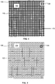
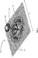
- FIGS. 1 to 5 example embodiments of an electronically tunable metasurface reflector 100 that can be used to implement a reflective antenna is shown in FIGS. 1 to 5 .
- the metasurface reflector 100 is a liquid-crystal-loaded tunable sheet providing a reflective phase that can be electronically reconfigured to allow effective antenna beam steering.
- the metasurface reflector 100 is a high-impedance surface and includes an upper surface or side 102 (shown in FIG. 1 ), a bottom surface or side 104 (shown in FIG. 2 ), and includes an array of addressable cells 106 for reflective beam steering antenna applications.
- the cells 106 are arranged to provide a two-dimensional periodical structure implementing an array of electrically small scatterers.
- the dimensions of the cells 106 are selected such that the periodicity of the cell array is relatively small compared to the operating wavelength of the radio waves that the metasurface reflector 100 is intended to reflect. In some examples, the cells have a periodicity that is less than a quarter of the minimum intended operating wavelength.
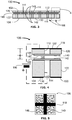
- FIG. 3 illustrates a side sectional view of a row of cells 106 of metasurface reflector 100
- FIG. 4 shows an enlarged side sectional view of one of the cells 106 as indicated by dashed box 4 in FIG. 3
- the metasurface reflector 100 includes an upper multi-layer double-sided printed circuit board (PCB) 120 and a lower multi-layer double sided PCB 122, which respectively define the upper and bottom sides 102, 104.
- a sub-operating wavelength layer of electronically tunable liquid crystal (LC) 146 is located between the upper and lower PCBs 120,122.
- LC electronically tunable liquid crystal
- Upper PCB 120 has a central non-conductive substrate layer (shown in cross-hatch in FIGs. 3 and 4 ).
- a gridded wire mesh 118 forms the top layer of the PCB 120, and a two dimensional array of conductive microstrip patches 140, each of which is surrounded by an insulating slot or gap 148, forms the bottom layer of the PCB 120.
- each microstrip patch 140 is electrically connected by a conductive plated-through hole (PTH) via 112 that extends from the center of the patch 140 through the PCB 120 substrate layer to a respective intersection point of wire mesh 118 such that wire mesh 118 provides a common DC return path for each of the microstrip patches 140.
- PTH conductive plated-through hole
- PTH vias 112 may be provided by forming and plating holes through the PCB 120 substrate layer
- microstrip patches 140 may be formed from etching gaps 148 from a conductive layer on the lower surface of PCB 120
- gridded wire mesh 118 may be similarly formed by etching a conductive layer on the upper layer of PCB 120.
- Lower PCB 122 has a central non-conductive substrate layer (shown in cross-hatch in FIGs. 3 and 4 ).
- a two dimensional array of conductive microstrip patches 142 which are each surrounded by an insulating slot or gap 148 and correspond in shape and periodicity to the upper PCB microstrip patches 140, form the top layer of lower PCB 122, and a conductive ground plane 130 forms the bottom layer of PCB 122.
- Each microstrip patch 142 is electrically connected to a respective conductive plated-through hole (PTH) via 114 that extends from the center of the patch 142 through the PCB 122 substrate layer to the ground plane 130 layer.
- PTH conductive plated-through hole
- the ground plane 130 includes an array of openings on the substrate layer that form a circular gap between the ground plane and the PTH vias 114 such that the ground plane 130 is electrically isolated from each of the PTH vias 114, permitting a unique control voltage to be applied to each PTH via 114.
- PTH vias 114 may be provided by forming and plating holes through the PCB 122 substrate layer
- microstrip patches 142 may be formed from etching gaps 148 from a conductive layer on the upper surface of PCB 120
- ground plane 130 may be similarly formed by etching a conductive layer on the lower layer of PCB 120 to provide insulated openings around each of the PTH vias 114.
- control voltages are provided to the lower microstrip patches 142 through PTH vias 114 that are accessible through the ground plane 130.
- Other embodiments could have different configurations, including a control line layer that could be integrated into substrate 122 to provide conductive control terminals to each of the microstrip patches 142.
- the upper and lower PCBs 120, 122 are located in spaced opposition to each other with an intermediate layer of liquid crystal 146 located between them.
- the upper PCB microstrip patches 140 and the lower PCB microstrip patches 142 align with each other to from an array of cell regions 144, each of which contains a volume of liquid crystal 146, thus providing an array of individually controllable, LC cell regions 144.
- each unit cell 106 includes a volume of tunable liquid crystal 146 that is located in region 144 between an upper conductive microstrip patch 140 and a lower conductive microstrip patch 142.
- Upper conductive microstrip patch 140 is connected by a respective conductive path (PTH via 112) to a common potential, namely wire mesh 118, and lower conductive microstrip patch 142 is connected to a control terminal (PTH via 114) that allows a unique control voltage from an adjustable DC voltage source 160 to be applied to the microstrip patch 142
- the metasurface reflector 100 has a resonant frequency that can depend on the geometry of the cells 106 and dielectric properties of the materials used in the PCBs 120, 122.
- the microstrip patches 140, 142 have rectangular surfaces (for example square) having a maximum normal dimension that is less than 1 ⁇ 4 of the minimum intended operating wavelength, however other microstrip patch configurations could be used.
- the microstrip patches 140, 142 may have dimensions that are less than quarter of a wavelength of the intended operating wavelength of the metasurface reflector 100.
- wire mesh 118 has a periodicity and grid dimensions that correspond to those of microstrip patches 140, with a grid intersection point occurring over a center point of each microstrip patch 140.
- the metasurface reflector 100 illustrated in Figs 1 to 5 provides a structure in which etching can be used to form the components of PCB boards 120, 122.
- liquid crystal 146 is can be placed between the PCB's 120, 122, which can then be secured together.
- the liquid crystal 146 is a nematic liquid crystal that has an intermediate nematic gel-like state between solid crystalline and liquid phase at the intended operating temperature range of the metasurface reflector 100.
- liquid crystal include, for example, GT3-23001 liquid crystal and BL038 liquid crystal from the Merck group.
- Liquid crystal 146 in a nematic state possesses dielectric anisotropy characteristics at microwave frequencies, whose effective dielectric constant may be adjusted by setting different orientations of the molecules of liquid crystal 146 relative to its reference axis.
- the liquid crystal 146 may change its dielectric properties due to different orientations of the molecules 602 caused by application of electrostatic field between the microstrip patches 140 and 142.
- the dielectric constant between the microstrip patches 140 and 142 at each unit cell 106 can be tuned by varying the DC voltage applied to patch 142, allowing the reflection phase at each individual unit cell 106 to be controlled.
- the unit cells 106 can be collectively controlled so that metasurface reflector 100 acts like a distributed spatial phase shifter that interacts with an incident wave and produces a reflected wave with varying phase shift across its aperture. Because reflection phase is determined by the frequency of the incoming wave with respect to the resonance frequency, the metasurface reflector 100 can be tuned to form a distributed 2D phase shifter. Therefore, an incoming wave may be redirected by adjusting DC voltages of unit cells 106 to give proper phase distribution for the desired direction of reflected wave.
- the metasurface reflector 100 has a relatively high density/small periodicity of cells 106.
- top PCB 120 is relatively thin, having a thickness h1 ⁇ /20 and the liquid crystal 146 in cell region 144 has a thickness of h2 ⁇ /20 (i.e. the gap between the opposed microstrip patches 140 and 142).
- the thicknesses h1 and h2 can be different from each other.
- the bottom PCB 122 has a finite thickness h3 ⁇ ⁇ /4.
- the reflection phase of an incident wave at the surface of the metasurface reflector 100 can be controlled by varying the DC voltages applied to unit cells 106 such that continuous beam steering of an EM wave can be achieved by regulating DC voltage distribution to unit cells 106 across the metasurface reflector 100.
- Example embodiments of LC reconfigurable metasurface reflector antennas will now be described. Although the reflector antenna embodiments described below incorporate LC reconfigurable metasurface reflector 100, it is possible that other LC reconfigurable metasurface configurations could also be suitable for use as a reflector in the antennas described below.
- FIGS. 6-8 show some possible antenna configurations for beam-steerable metasurface reflector antennas, according to example embodiments.
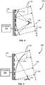
- Fig. 6 illustrates prime-focus beam-steerable metasurface antenna 170, where a feed structure 172 for generating an RF signal is placed in the front center of a metasurface reflector 100.
- Fig. 7 shows an offset feed beam steerable metasurface reflector antenna 180, where a single RF feed structure 172 is placed at an offset location from the front center of a metasurface reflector 100.
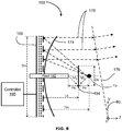
- Fig. 8 shows a dual-reflector metasurface antenna 190 with a central RF feed structure 192, where a flat sub-reflector 194 is placed in the front center of a metasurface reflector 100.
- liquid-crystal-loaded flat metasurface reflector 100 is used to provide the necessary parabolic phase distribution (represented by parabola 174) across the surface of the metasurface reflector, including phase offset required for beam collimation and possible beam tilt, ⁇ o, required to provide the reflected wave-front represented by line 176.
- the required phase distribution on the metasurface reflector can be computed using path delay of wave propagation between the feed structure 172, 192 and the metasurface reflector 100.
- a controller 165 is configured to control the DC voltage applied across each of the unit cells 106 in the metasurface reflector 100 to achieve the required phase distribution.
- prime-feed metasurface reflector antenna 190 will be described in greater detail, however it will be noted that the general geometrical parameters discussed below in respect of the dual reflector antenna of Fig. 8 are also applicable to the single reflector antennas of Figs. 6 and 7 .
- the feed structure 172 is placed at the focal point of the metasurface reflector 100.
- a flat metallic sub-reflector 194 is used and the metasurface reflector 100 is designed to have phase distribution 174 such that its focus point F p falls at the mirror image of the phase center of the sub-reflector structure 194.
- Controller 165 can apply DC voltages to unit cells 106 required to achieve the calculated phase distribution.
- the calculations can be ongoing to provide adaptive phase compensation across the metasurface reflector 100, allowing the reflector to be continuously shaped for optimum amplitude taper to give optimum beam performance.
- controller 265 comprises a processor and an associated digital storage that stores instructions and data for the processor to enable the beam steering functionality described herein.
- controller 265 may comprise a programmable logic controller.
- the metasurface reflector antennas 170, 180, and 190 can be operated to both transmit and receive RF signals.
- the RF feed structure 172, 192 converts electric currents from a transmitter circuit into wireless RF waves that are reflected by the metasurface reflector 100
- the RF feed structure 172, 192 converts RF waves reflected by the metasurface reflector 100 into electric currents for a receiver circuit.
- the metasurface reflector antennas 170, 180, and 190 may be used as transmit-only or receive-only antennas.
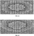
- Fig. 9 shows an example of a dual-reflector antenna 190 using a flat sub-reflector liquid-crystal-loaded metasurface reflector 100.
- This example is simulated using a full-wave finite element EM simulator, HFSS.
- Figs. 10 and 11 show simulated reflection phase distribution across the cells 106 on the metasurface reflector 100 for 0deg and 15 deg tilt angle cases.
- Figs. 12 and 13 give simulated effective dielectric constant distributions of liquid crystal in the cells 106 of metasurface reflector 100 for tilt angle 0deg and 15 deg.
- Figs. 14 and 15 gives simulated radiation patterns of the dual-reflector metasurface antenna 190.
- Fig. 16 shows an method of beam steering that can be carried out using a reflector antenna such as antnna 170, 180 or 190 according to an example not forming part of the claimed invention.
- the method includes generating an RF signal at a feed (for example feed structure 172 or 192) for application to a metasurface reflector 100 comprising a two dimensional array of cells 106 each including a volume of liquid crystal 146.
- the method also includes reflecting the applied RF signal off of the metasurface reflector 100 (step 1604) and adjusting voltages to control terminals 114 associated with a plurality of the cells of the metasurface to adjust a phase of the reflected RF signal by adjusting an orientation of the molecules of the liquid crystal within each cell (step 1606).
- example embodiments disclose individually addressable cells, other embodiments may have cells that may be addressable by row or column or in a multiplexed manner.
- the metasurface may have any arbitrary orientation.
Landscapes
- Physics & Mathematics (AREA)
- Electromagnetism (AREA)
- Optics & Photonics (AREA)
- Aerials With Secondary Devices (AREA)
- Variable-Direction Aerials And Aerial Arrays (AREA)
- Waveguide Aerials (AREA)
Claims (5)
- Reflektorantenne, die Folgendes umfasst:• eine Einspeisung (172) zum Erzeugen eines Hochfrequenzsignals bzw. HF-Signals; und• einen Metaoberflächenreflektor (100) zum Reflektieren des HF-Signals, das von der Einspeisung (172) ausgeht, wobei der Metaoberflächenreflektor (100) ein Array von Zellen umfasst, die jeweils ein Flüssigkristallvolumen mit einem steuerbaren dielektrischen Wert aufweisen, der so ausgelegt ist, dass er eine Reflexionsphase der Zellen ermöglicht, damit die Zellen selektiv abgestimmt werden können, um Strahllenkung des reflektierten HF-Signals zu bewirken,wobei der Metaoberflächenreflektor (100) Folgendes umfasst:∘ ein erstes und ein zweites doppelseitiges Substrat, die eine Intermediärregion zwischen ihnen definieren, die Flüssigkristall in einer nematischen Phase enthält;∘ wobei das erste Substrat ein erstes Mikrostreifenpatch-Array (140) aufweist, das an einer Seite davon ausgebildet ist, die dem zweiten Substrat zugewandt ist, wobei das erste Mikrostreifenpatch-Array (140) ein zweidimensionales Array von Mikrostreifenpatches umfasst, die jeweils elektrisch mit einem gemeinsamen Potential verbunden sind; und∘ wobei das zweite doppelseitige Substrat ein zweites Mikrostreifenpatch-Array (142) aufweist, das an einer Seite davon ausgebildet ist, die dem ersten Substrat zugewandt ist, wobei das zweite Mikrostreifenpatch-Array (142) ein zweidimensionales Array von Mikrostreifenpatches umfasst, die jeweils einen jeweiligen leitenden Anschluss aufweisen; wobei das erste Mikrostreifenpatch-Array (140) und das zweite Mikrostreifenpatch-Array (142) ausgerichtet sind, um das Array von Zellen auszubilden, wobei jede Zelle einen Mikrostreifenpatch des ersten Mikrostreifenpatch-Arrays (140), angeordnet in einer beabstandeten Gegenüberstellung zu einem Mikrostreifenpatch des zweiten Mikrostreifenpatch-Arrays (142) mit dem dazwischen befindlichen Flüssigkristallvolumen umfasst, wobei der leitende Anschluss an den Mikrostreifenpatch des zweiten Mikrostreifenpatch-Arrays (142) derart ausgelegt ist, dass er zulässt, dass eine Steuerspannung an die Zelle angelegt werden kann, um den dielektrischen Wert des Flüssigkristallvolumens zu steuern, wodurch zugelassen wird, dass die Reflexionsphase der Zelle selektiv abgestimmt werden kann,∘ wobei der Metaoberflächenreflektor ein gitterförmiges Drahtnetz (118) auf dem ersten Substrat umfasst, wobei jeder der Mikrostreifenpatches des ersten Mikrostreifenpatch-Arrays (140) elektrisch mit einem jeweiligen Punkt des gitterförmigen Drahtnetzes (118) verbunden ist, um das gemeinsame Potential bereitzustellen.
- Reflektorantenne nach Anspruch 1, wobei die Antenne eine Primärfokus-Reflektorantenne mit der Einspeisung, die das HF-Signal erzeugt, zum Metaoberflächenreflektor ist.
- Reflektorantenne nach Anspruch 2, wobei die Einspeisung gegenüber einer Mitte des Metaoberflächenreflektors versetzt ist.
- Reflektorantenne nach Anspruch 1, wobei die Antenne eine Doppelreflektorantenne mit der Einspeisung, die das HF-Signal erzeugt, zu einem Subreflektor, der das HF-Signal zum Metaoberflächenreflektor reflektiert, ist.
- Reflektorantenne nach einem der Ansprüche 1 bis 4, wobei das gitterförmige Drahtnetz auf einer Seite des ersten Substrats ausgebildet ist, das der Seite, auf der das erste Mikrostreifenpatch-Array ausgebildet ist, gegenüberliegt, wobei jeder der Mikrostreifenpatches des ersten Mikrostreifenpatch-Arrays durch ein jeweiliges plattiertes Durchgangsloch, das sich durch das erste Substrat erstreckt, mit dem gitterförmigen Drahtnetz elektrisch verbunden ist.
Applications Claiming Priority (3)
| Application Number | Priority Date | Filing Date | Title |
|---|---|---|---|
| US201662409710P | 2016-10-18 | 2016-10-18 | |
| US15/630,396 US10490903B2 (en) | 2016-10-18 | 2017-06-22 | Liquid-crystal reconfigurable metasurface reflector antenna |
| PCT/CN2017/105688 WO2018072627A1 (en) | 2016-10-18 | 2017-10-11 | Liquid-crystal reconfigurable metasurface reflector antenna |
Publications (3)
| Publication Number | Publication Date |
|---|---|
| EP3520173A1 EP3520173A1 (de) | 2019-08-07 |
| EP3520173A4 EP3520173A4 (de) | 2019-10-02 |
| EP3520173B1 true EP3520173B1 (de) | 2021-09-22 |
Family
ID=61904114
Family Applications (1)
| Application Number | Title | Priority Date | Filing Date |
|---|---|---|---|
| EP17862787.3A Active EP3520173B1 (de) | 2016-10-18 | 2017-10-11 | Flüssigkristalline rekonfigurierbare metaoberflächenreflektorantenne |
Country Status (4)
| Country | Link |
|---|---|
| US (1) | US10490903B2 (de) |
| EP (1) | EP3520173B1 (de) |
| CN (1) | CN109891673B (de) |
| WO (1) | WO2018072627A1 (de) |
Families Citing this family (26)
| Publication number | Priority date | Publication date | Assignee | Title |
|---|---|---|---|---|
| JP2019197098A (ja) * | 2018-05-08 | 2019-11-14 | 浜松ホトニクス株式会社 | メタサーフェス構造体及びメタサーフェス構造体の製造方法 |
| CN108808252B (zh) * | 2018-06-08 | 2020-11-03 | 西安电子科技大学 | 基于超表面的格里高利天线 |
| US10581158B2 (en) * | 2018-07-19 | 2020-03-03 | Huawei Technologies Co., Ltd. | Electronically beam-steerable, low-sidelobe composite right-left-handed (CRLH) metamaterial array antenna |
| CN110739527B (zh) * | 2018-07-19 | 2022-02-18 | 华为技术有限公司 | 一种波束重构方法、天线、微波设备和网络系统 |
| CN110828980B (zh) * | 2018-08-09 | 2021-10-29 | 中国科学院理化技术研究所 | 一种液态金属可重构天线及其重构方法 |
| US11923617B2 (en) * | 2018-10-31 | 2024-03-05 | Nokia Technologies Oy | Apparatus for reflecting electromagnetic waves and method of operating such apparatus |
| CN109273846A (zh) * | 2018-11-08 | 2019-01-25 | 中国电子科技集团公司第五十四研究所 | 一种基于透射式相控电磁表面的可重构阵列天线 |
| WO2020110375A1 (ja) * | 2018-11-27 | 2020-06-04 | 三菱電機株式会社 | アンテナ装置及びアンテナ調整方法 |
| CN110380222B (zh) * | 2019-06-17 | 2021-05-11 | 东南大学 | 一种惠更斯超表面单元、透射阵天线及单元相位控制方法 |
| US11394111B1 (en) * | 2019-08-14 | 2022-07-19 | Notch, Inc. | Electronically reconfigurable antenna |
| US10727601B1 (en) * | 2019-11-13 | 2020-07-28 | Lumotive, LLC | Sidelobe suppression in metasurface devices |
| US11217888B2 (en) | 2019-11-18 | 2022-01-04 | i5 Technologies, Inc. | Reconfigurable antenna array of individual reconfigurable antennas |
| CN111180903A (zh) * | 2020-02-17 | 2020-05-19 | Oppo广东移动通信有限公司 | 天线组件和电子设备 |
| US20230208104A1 (en) * | 2020-05-08 | 2023-06-29 | President And Fellows Of Harvard College | Wavelength tunable metasurface based external cavity laser |
| US11658411B2 (en) | 2020-07-09 | 2023-05-23 | Dr. Alan Evans Business and Scientific Consulting, LLC | Electrically-controlled RF, microwave, and millimeter wave devices using tunable material-filled vias |
| CN111969328B (zh) * | 2020-07-24 | 2022-07-08 | 广西科技大学 | 一种基于双层超表面的高性能oam波束发生器 |
| US11843171B2 (en) * | 2020-08-18 | 2023-12-12 | Samsung Electronics Co., Ltd. | Multi-layer reconfigurable surface for an antenna |
| US20230411844A1 (en) * | 2020-11-09 | 2023-12-21 | Latys Intelligence Inc. | Nonreciprocal beam steerable metasurfaces |
| JP2024503859A (ja) * | 2021-01-14 | 2024-01-29 | ラティス・インテリジェンス・インコーポレイテッド | 反射型ビームステアリングメタ表面 |
| CN113488776A (zh) * | 2021-05-07 | 2021-10-08 | 维沃移动通信有限公司 | 超表面结构 |
| KR102467623B1 (ko) | 2021-07-05 | 2022-11-17 | 서울대학교산학협력단 | 액정 기반 리플렉트어레이 안테나 |
| CN113629389B (zh) * | 2021-08-18 | 2022-04-26 | 北京星英联微波科技有限责任公司 | 1-bit相位可重构变极化全金属反射阵列天线单元 |
| EP4160820A1 (de) * | 2021-09-30 | 2023-04-05 | Siemens AG Österreich | Funk-kommunikations-system |
| CN116826384A (zh) * | 2022-03-21 | 2023-09-29 | 中兴通讯股份有限公司 | 超表面单元及其基站 |
| US11927769B2 (en) | 2022-03-31 | 2024-03-12 | Metalenz, Inc. | Polarization sorting metasurface microlens array device |
| WO2024141984A1 (en) * | 2022-12-28 | 2024-07-04 | Ariel Scientific Innovations Ltd. | Antenna reflector |
Family Cites Families (8)
| Publication number | Priority date | Publication date | Assignee | Title |
|---|---|---|---|---|
| US6552696B1 (en) * | 2000-03-29 | 2003-04-22 | Hrl Laboratories, Llc | Electronically tunable reflector |
| US9871293B2 (en) * | 2010-11-03 | 2018-01-16 | The Boeing Company | Two-dimensionally electronically-steerable artificial impedance surface antenna |
| ES2388213B2 (es) | 2010-12-16 | 2013-01-29 | Universidad Politécnica de Madrid | Antena reflectarray de haz reconfigurable para frecuencias en los rangos de terahercios y de ondas milimétricas. |
| EP2575211B1 (de) * | 2011-09-27 | 2014-11-05 | Technische Universität Darmstadt | Elektronisch steuerbare Planarphasen-Arrayantenne |
| US9843103B2 (en) | 2014-03-26 | 2017-12-12 | Elwha Llc | Methods and apparatus for controlling a surface scattering antenna array |
| US9837695B2 (en) * | 2014-08-01 | 2017-12-05 | The Boeing Company | Surface-wave waveguide with conductive sidewalls and application in antennas |
| US9893435B2 (en) | 2015-02-11 | 2018-02-13 | Kymeta Corporation | Combined antenna apertures allowing simultaneous multiple antenna functionality |
| EP3062392A1 (de) | 2015-02-24 | 2016-08-31 | Fraunhofer-Gesellschaft zur Förderung der angewandten Forschung e.V. | Reflektor mit einer elektronischen Schaltung und Antennenvorrichtung mit einem Reflektor |
-
2017
- 2017-06-22 US US15/630,396 patent/US10490903B2/en active Active
- 2017-10-11 CN CN201780064495.6A patent/CN109891673B/zh active Active
- 2017-10-11 EP EP17862787.3A patent/EP3520173B1/de active Active
- 2017-10-11 WO PCT/CN2017/105688 patent/WO2018072627A1/en unknown
Also Published As
| Publication number | Publication date |
|---|---|
| CN109891673A (zh) | 2019-06-14 |
| CN109891673B (zh) | 2020-09-04 |
| US10490903B2 (en) | 2019-11-26 |
| EP3520173A4 (de) | 2019-10-02 |
| EP3520173A1 (de) | 2019-08-07 |
| US20180109002A1 (en) | 2018-04-19 |
| WO2018072627A1 (en) | 2018-04-26 |
Similar Documents
| Publication | Publication Date | Title |
|---|---|---|
| EP3520173B1 (de) | Flüssigkristalline rekonfigurierbare metaoberflächenreflektorantenne | |
| US10211532B2 (en) | Liquid-crystal reconfigurable multi-beam phased array | |
| US10720712B2 (en) | Liquid-crystal tunable metasurface for beam steering antennas | |
| US11695204B2 (en) | Dynamic polarization and coupling control from a steerable multi-layered cylindrically fed holographic antenna | |
| EP3850706B1 (de) | Elektronisch lenkbare holographische antenne mit rekonfigurierbaren strahlern für breitbandige frequenzabstimmung | |
| Foo | Liquid-crystal reconfigurable metasurface reflectors | |
| EP3108538B1 (de) | Dynamische polarisation und steckkontrolle für eine lenkbare und zylindrisch gespeiste holografische antenne | |
| CN109923735B (zh) | 平板天线的定向耦合器馈电 | |
| CN112106252A (zh) | 孔径天线的阻抗匹配 | |
| EP3811467B1 (de) | Elektronisch strahllenkbare gruppenantenne aus zusammengesetztem rechts-links-händigem (crlh) metamaterial mit niedriger nebenkeule | |
| EP3928381B1 (de) | Flache schwenkbare planare leckwellen-gruppenantenne mit niedriger nebenkeule | |
| Horestani et al. | A Wideband Rotary-Joint-Free H-Plane Horn Antenna With 360° Steerable Radiation Pattern Using Gap Waveguide Technology | |
| Foo | Liquid-crystal reconfigurable, lens-enhanced, millimeter-wave phased array | |
| Nabeel et al. | Investigating Square Slot Unit Cell for Low-Cost Phase-Gradient Metasurfaces | |
| Joy et al. | Modern Reflectarray Antennas: A Review of the Design, State-of-the-Art, and Research Challenges |
Legal Events
| Date | Code | Title | Description |
|---|---|---|---|
| STAA | Information on the status of an ep patent application or granted ep patent |
Free format text: STATUS: THE INTERNATIONAL PUBLICATION HAS BEEN MADE |
|
| PUAI | Public reference made under article 153(3) epc to a published international application that has entered the european phase |
Free format text: ORIGINAL CODE: 0009012 |
|
| STAA | Information on the status of an ep patent application or granted ep patent |
Free format text: STATUS: REQUEST FOR EXAMINATION WAS MADE |
|
| 17P | Request for examination filed |
Effective date: 20190429 |
|
| AK | Designated contracting states |
Kind code of ref document: A1 Designated state(s): AL AT BE BG CH CY CZ DE DK EE ES FI FR GB GR HR HU IE IS IT LI LT LU LV MC MK MT NL NO PL PT RO RS SE SI SK SM TR |
|
| AX | Request for extension of the european patent |
Extension state: BA ME |
|
| REG | Reference to a national code |
Ref country code: DE Ref legal event code: R079 Ref document number: 602017046535 Country of ref document: DE Free format text: PREVIOUS MAIN CLASS: H01Q0015020000 Ipc: H01Q0019130000 |
|
| A4 | Supplementary search report drawn up and despatched |
Effective date: 20190830 |
|
| RIC1 | Information provided on ipc code assigned before grant |
Ipc: H01Q 19/19 20060101ALI20190826BHEP Ipc: H01Q 21/06 20060101ALI20190826BHEP Ipc: H01Q 3/46 20060101ALI20190826BHEP Ipc: H01Q 19/13 20060101AFI20190826BHEP Ipc: H01Q 15/00 20060101ALI20190826BHEP Ipc: H01Q 15/14 20060101ALI20190826BHEP |
|
| DAV | Request for validation of the european patent (deleted) | ||
| DAX | Request for extension of the european patent (deleted) | ||
| GRAP | Despatch of communication of intention to grant a patent |
Free format text: ORIGINAL CODE: EPIDOSNIGR1 |
|
| STAA | Information on the status of an ep patent application or granted ep patent |
Free format text: STATUS: GRANT OF PATENT IS INTENDED |
|
| INTG | Intention to grant announced |
Effective date: 20210520 |
|
| GRAS | Grant fee paid |
Free format text: ORIGINAL CODE: EPIDOSNIGR3 |
|
| GRAA | (expected) grant |
Free format text: ORIGINAL CODE: 0009210 |
|
| STAA | Information on the status of an ep patent application or granted ep patent |
Free format text: STATUS: THE PATENT HAS BEEN GRANTED |
|
| AK | Designated contracting states |
Kind code of ref document: B1 Designated state(s): AL AT BE BG CH CY CZ DE DK EE ES FI FR GB GR HR HU IE IS IT LI LT LU LV MC MK MT NL NO PL PT RO RS SE SI SK SM TR |
|
| REG | Reference to a national code |
Ref country code: GB Ref legal event code: FG4D |
|
| REG | Reference to a national code |
Ref country code: IE Ref legal event code: FG4D |
|
| REG | Reference to a national code |
Ref country code: DE Ref legal event code: R096 Ref document number: 602017046535 Country of ref document: DE |
|
| REG | Reference to a national code |
Ref country code: CH Ref legal event code: EP Ref country code: AT Ref legal event code: REF Ref document number: 1433028 Country of ref document: AT Kind code of ref document: T Effective date: 20211015 |
|
| REG | Reference to a national code |
Ref country code: LT Ref legal event code: MG9D |
|
| REG | Reference to a national code |
Ref country code: NL Ref legal event code: MP Effective date: 20210922 |
|
| PG25 | Lapsed in a contracting state [announced via postgrant information from national office to epo] |
Ref country code: NO Free format text: LAPSE BECAUSE OF FAILURE TO SUBMIT A TRANSLATION OF THE DESCRIPTION OR TO PAY THE FEE WITHIN THE PRESCRIBED TIME-LIMIT Effective date: 20211222 Ref country code: LT Free format text: LAPSE BECAUSE OF FAILURE TO SUBMIT A TRANSLATION OF THE DESCRIPTION OR TO PAY THE FEE WITHIN THE PRESCRIBED TIME-LIMIT Effective date: 20210922 Ref country code: BG Free format text: LAPSE BECAUSE OF FAILURE TO SUBMIT A TRANSLATION OF THE DESCRIPTION OR TO PAY THE FEE WITHIN THE PRESCRIBED TIME-LIMIT Effective date: 20211222 Ref country code: HR Free format text: LAPSE BECAUSE OF FAILURE TO SUBMIT A TRANSLATION OF THE DESCRIPTION OR TO PAY THE FEE WITHIN THE PRESCRIBED TIME-LIMIT Effective date: 20210922 Ref country code: FI Free format text: LAPSE BECAUSE OF FAILURE TO SUBMIT A TRANSLATION OF THE DESCRIPTION OR TO PAY THE FEE WITHIN THE PRESCRIBED TIME-LIMIT Effective date: 20210922 Ref country code: RS Free format text: LAPSE BECAUSE OF FAILURE TO SUBMIT A TRANSLATION OF THE DESCRIPTION OR TO PAY THE FEE WITHIN THE PRESCRIBED TIME-LIMIT Effective date: 20210922 Ref country code: SE Free format text: LAPSE BECAUSE OF FAILURE TO SUBMIT A TRANSLATION OF THE DESCRIPTION OR TO PAY THE FEE WITHIN THE PRESCRIBED TIME-LIMIT Effective date: 20210922 |
|
| REG | Reference to a national code |
Ref country code: AT Ref legal event code: MK05 Ref document number: 1433028 Country of ref document: AT Kind code of ref document: T Effective date: 20210922 |
|
| PG25 | Lapsed in a contracting state [announced via postgrant information from national office to epo] |
Ref country code: LV Free format text: LAPSE BECAUSE OF FAILURE TO SUBMIT A TRANSLATION OF THE DESCRIPTION OR TO PAY THE FEE WITHIN THE PRESCRIBED TIME-LIMIT Effective date: 20210922 Ref country code: GR Free format text: LAPSE BECAUSE OF FAILURE TO SUBMIT A TRANSLATION OF THE DESCRIPTION OR TO PAY THE FEE WITHIN THE PRESCRIBED TIME-LIMIT Effective date: 20211223 |
|
| PG25 | Lapsed in a contracting state [announced via postgrant information from national office to epo] |
Ref country code: AT Free format text: LAPSE BECAUSE OF FAILURE TO SUBMIT A TRANSLATION OF THE DESCRIPTION OR TO PAY THE FEE WITHIN THE PRESCRIBED TIME-LIMIT Effective date: 20210922 |
|
| REG | Reference to a national code |
Ref country code: CH Ref legal event code: PL |
|
| PG25 | Lapsed in a contracting state [announced via postgrant information from national office to epo] |
Ref country code: IS Free format text: LAPSE BECAUSE OF FAILURE TO SUBMIT A TRANSLATION OF THE DESCRIPTION OR TO PAY THE FEE WITHIN THE PRESCRIBED TIME-LIMIT Effective date: 20220122 Ref country code: SK Free format text: LAPSE BECAUSE OF FAILURE TO SUBMIT A TRANSLATION OF THE DESCRIPTION OR TO PAY THE FEE WITHIN THE PRESCRIBED TIME-LIMIT Effective date: 20210922 Ref country code: RO Free format text: LAPSE BECAUSE OF FAILURE TO SUBMIT A TRANSLATION OF THE DESCRIPTION OR TO PAY THE FEE WITHIN THE PRESCRIBED TIME-LIMIT Effective date: 20210922 Ref country code: PT Free format text: LAPSE BECAUSE OF FAILURE TO SUBMIT A TRANSLATION OF THE DESCRIPTION OR TO PAY THE FEE WITHIN THE PRESCRIBED TIME-LIMIT Effective date: 20220124 Ref country code: PL Free format text: LAPSE BECAUSE OF FAILURE TO SUBMIT A TRANSLATION OF THE DESCRIPTION OR TO PAY THE FEE WITHIN THE PRESCRIBED TIME-LIMIT Effective date: 20210922 Ref country code: NL Free format text: LAPSE BECAUSE OF FAILURE TO SUBMIT A TRANSLATION OF THE DESCRIPTION OR TO PAY THE FEE WITHIN THE PRESCRIBED TIME-LIMIT Effective date: 20210922 Ref country code: ES Free format text: LAPSE BECAUSE OF FAILURE TO SUBMIT A TRANSLATION OF THE DESCRIPTION OR TO PAY THE FEE WITHIN THE PRESCRIBED TIME-LIMIT Effective date: 20210922 Ref country code: EE Free format text: LAPSE BECAUSE OF FAILURE TO SUBMIT A TRANSLATION OF THE DESCRIPTION OR TO PAY THE FEE WITHIN THE PRESCRIBED TIME-LIMIT Effective date: 20210922 Ref country code: CZ Free format text: LAPSE BECAUSE OF FAILURE TO SUBMIT A TRANSLATION OF THE DESCRIPTION OR TO PAY THE FEE WITHIN THE PRESCRIBED TIME-LIMIT Effective date: 20210922 Ref country code: AL Free format text: LAPSE BECAUSE OF FAILURE TO SUBMIT A TRANSLATION OF THE DESCRIPTION OR TO PAY THE FEE WITHIN THE PRESCRIBED TIME-LIMIT Effective date: 20210922 |
|
| REG | Reference to a national code |
Ref country code: DE Ref legal event code: R097 Ref document number: 602017046535 Country of ref document: DE Ref country code: BE Ref legal event code: MM Effective date: 20211031 |
|
| PG25 | Lapsed in a contracting state [announced via postgrant information from national office to epo] |
Ref country code: MC Free format text: LAPSE BECAUSE OF FAILURE TO SUBMIT A TRANSLATION OF THE DESCRIPTION OR TO PAY THE FEE WITHIN THE PRESCRIBED TIME-LIMIT Effective date: 20210922 |
|
| PG25 | Lapsed in a contracting state [announced via postgrant information from national office to epo] |
Ref country code: LU Free format text: LAPSE BECAUSE OF NON-PAYMENT OF DUE FEES Effective date: 20211011 Ref country code: DK Free format text: LAPSE BECAUSE OF FAILURE TO SUBMIT A TRANSLATION OF THE DESCRIPTION OR TO PAY THE FEE WITHIN THE PRESCRIBED TIME-LIMIT Effective date: 20210922 Ref country code: BE Free format text: LAPSE BECAUSE OF NON-PAYMENT OF DUE FEES Effective date: 20211031 |
|
| PLBE | No opposition filed within time limit |
Free format text: ORIGINAL CODE: 0009261 |
|
| STAA | Information on the status of an ep patent application or granted ep patent |
Free format text: STATUS: NO OPPOSITION FILED WITHIN TIME LIMIT |
|
| 26N | No opposition filed |
Effective date: 20220623 |
|
| PG25 | Lapsed in a contracting state [announced via postgrant information from national office to epo] |
Ref country code: LI Free format text: LAPSE BECAUSE OF NON-PAYMENT OF DUE FEES Effective date: 20211031 Ref country code: CH Free format text: LAPSE BECAUSE OF NON-PAYMENT OF DUE FEES Effective date: 20211031 |
|
| PG25 | Lapsed in a contracting state [announced via postgrant information from national office to epo] |
Ref country code: IE Free format text: LAPSE BECAUSE OF NON-PAYMENT OF DUE FEES Effective date: 20211011 |
|
| PG25 | Lapsed in a contracting state [announced via postgrant information from national office to epo] |
Ref country code: SI Free format text: LAPSE BECAUSE OF FAILURE TO SUBMIT A TRANSLATION OF THE DESCRIPTION OR TO PAY THE FEE WITHIN THE PRESCRIBED TIME-LIMIT Effective date: 20210922 |
|
| PG25 | Lapsed in a contracting state [announced via postgrant information from national office to epo] |
Ref country code: IT Free format text: LAPSE BECAUSE OF FAILURE TO SUBMIT A TRANSLATION OF THE DESCRIPTION OR TO PAY THE FEE WITHIN THE PRESCRIBED TIME-LIMIT Effective date: 20210922 |
|
| PG25 | Lapsed in a contracting state [announced via postgrant information from national office to epo] |
Ref country code: CY Free format text: LAPSE BECAUSE OF FAILURE TO SUBMIT A TRANSLATION OF THE DESCRIPTION OR TO PAY THE FEE WITHIN THE PRESCRIBED TIME-LIMIT Effective date: 20210922 |
|
| PG25 | Lapsed in a contracting state [announced via postgrant information from national office to epo] |
Ref country code: SM Free format text: LAPSE BECAUSE OF FAILURE TO SUBMIT A TRANSLATION OF THE DESCRIPTION OR TO PAY THE FEE WITHIN THE PRESCRIBED TIME-LIMIT Effective date: 20210922 Ref country code: HU Free format text: LAPSE BECAUSE OF FAILURE TO SUBMIT A TRANSLATION OF THE DESCRIPTION OR TO PAY THE FEE WITHIN THE PRESCRIBED TIME-LIMIT; INVALID AB INITIO Effective date: 20171011 |
|
| PGFP | Annual fee paid to national office [announced via postgrant information from national office to epo] |
Ref country code: GB Payment date: 20230831 Year of fee payment: 7 |
|
| PGFP | Annual fee paid to national office [announced via postgrant information from national office to epo] |
Ref country code: FR Payment date: 20230911 Year of fee payment: 7 |
|
| PGFP | Annual fee paid to national office [announced via postgrant information from national office to epo] |
Ref country code: DE Payment date: 20230830 Year of fee payment: 7 |
|
| PG25 | Lapsed in a contracting state [announced via postgrant information from national office to epo] |
Ref country code: MK Free format text: LAPSE BECAUSE OF FAILURE TO SUBMIT A TRANSLATION OF THE DESCRIPTION OR TO PAY THE FEE WITHIN THE PRESCRIBED TIME-LIMIT Effective date: 20210922 |
|
| PG25 | Lapsed in a contracting state [announced via postgrant information from national office to epo] |
Ref country code: TR Free format text: LAPSE BECAUSE OF FAILURE TO SUBMIT A TRANSLATION OF THE DESCRIPTION OR TO PAY THE FEE WITHIN THE PRESCRIBED TIME-LIMIT Effective date: 20210922 |