EP3520171B1 - Sonde für passive intermodulation (pim) - Google Patents
Sonde für passive intermodulation (pim) Download PDFInfo
- Publication number
- EP3520171B1 EP3520171B1 EP17857254.1A EP17857254A EP3520171B1 EP 3520171 B1 EP3520171 B1 EP 3520171B1 EP 17857254 A EP17857254 A EP 17857254A EP 3520171 B1 EP3520171 B1 EP 3520171B1
- Authority
- EP
- European Patent Office
- Prior art keywords
- pim
- antenna
- test system
- probe
- wand
- Prior art date
- Legal status (The legal status is an assumption and is not a legal conclusion. Google has not performed a legal analysis and makes no representation as to the accuracy of the status listed.)
- Active
Links
Images


Classifications
-
- G—PHYSICS
- G01—MEASURING; TESTING
- G01R—MEASURING ELECTRIC VARIABLES; MEASURING MAGNETIC VARIABLES
- G01R29/00—Arrangements for measuring or indicating electric quantities not covered by groups G01R19/00 - G01R27/00
- G01R29/08—Measuring electromagnetic field characteristics
- G01R29/0807—Measuring electromagnetic field characteristics characterised by the application
- G01R29/0814—Field measurements related to measuring influence on or from apparatus, components or humans, e.g. in ESD, EMI, EMC, EMP testing, measuring radiation leakage; detecting presence of micro- or radiowave emitters; dosimetry; testing shielding; measurements related to lightning
-
- G—PHYSICS
- G01—MEASURING; TESTING
- G01R—MEASURING ELECTRIC VARIABLES; MEASURING MAGNETIC VARIABLES
- G01R29/00—Arrangements for measuring or indicating electric quantities not covered by groups G01R19/00 - G01R27/00
- G01R29/08—Measuring electromagnetic field characteristics
- G01R29/0864—Measuring electromagnetic field characteristics characterised by constructional or functional features
- G01R29/0878—Sensors; antennas; probes; detectors
-
- H—ELECTRICITY
- H01—ELECTRIC ELEMENTS
- H01Q—ANTENNAS, i.e. RADIO AERIALS
- H01Q1/00—Details of, or arrangements associated with, antennas
- H01Q1/12—Supports; Mounting means
- H01Q1/22—Supports; Mounting means by structural association with other equipment or articles
- H01Q1/24—Supports; Mounting means by structural association with other equipment or articles with receiving set
- H01Q1/241—Supports; Mounting means by structural association with other equipment or articles with receiving set used in mobile communications, e.g. GSM
- H01Q1/242—Supports; Mounting means by structural association with other equipment or articles with receiving set used in mobile communications, e.g. GSM specially adapted for hand-held use
-
- H—ELECTRICITY
- H01—ELECTRIC ELEMENTS
- H01Q—ANTENNAS, i.e. RADIO AERIALS
- H01Q1/00—Details of, or arrangements associated with, antennas
- H01Q1/36—Structural form of radiating elements, e.g. cone, spiral, umbrella; Particular materials used therewith
- H01Q1/38—Structural form of radiating elements, e.g. cone, spiral, umbrella; Particular materials used therewith formed by a conductive layer on an insulating support
-
- H—ELECTRICITY
- H01—ELECTRIC ELEMENTS
- H01Q—ANTENNAS, i.e. RADIO AERIALS
- H01Q21/00—Antenna arrays or systems
- H01Q21/29—Combinations of different interacting antenna units for giving a desired directional characteristic
-
- H—ELECTRICITY
- H01—ELECTRIC ELEMENTS
- H01Q—ANTENNAS, i.e. RADIO AERIALS
- H01Q7/00—Loop antennas with a substantially uniform current distribution around the loop and having a directional radiation pattern in a plane perpendicular to the plane of the loop
-
- H—ELECTRICITY
- H04—ELECTRIC COMMUNICATION TECHNIQUE
- H04W—WIRELESS COMMUNICATION NETWORKS
- H04W24/00—Supervisory, monitoring or testing arrangements
- H04W24/06—Testing, supervising or monitoring using simulated traffic
-
- H—ELECTRICITY
- H04—ELECTRIC COMMUNICATION TECHNIQUE
- H04W—WIRELESS COMMUNICATION NETWORKS
- H04W24/00—Supervisory, monitoring or testing arrangements
- H04W24/08—Testing, supervising or monitoring using real traffic
-
- H—ELECTRICITY
- H01—ELECTRIC ELEMENTS
- H01Q—ANTENNAS, i.e. RADIO AERIALS
- H01Q1/00—Details of, or arrangements associated with, antennas
- H01Q1/42—Housings not intimately mechanically associated with radiating elements, e.g. radome
-
- H—ELECTRICITY
- H01—ELECTRIC ELEMENTS
- H01Q—ANTENNAS, i.e. RADIO AERIALS
- H01Q5/00—Arrangements for simultaneous operation of antennas on two or more different wavebands, e.g. dual-band or multi-band arrangements
- H01Q5/30—Arrangements for providing operation on different wavebands
-
- H—ELECTRICITY
- H04—ELECTRIC COMMUNICATION TECHNIQUE
- H04L—TRANSMISSION OF DIGITAL INFORMATION, e.g. TELEGRAPHIC COMMUNICATION
- H04L43/00—Arrangements for monitoring or testing data switching networks
- H04L43/50—Testing arrangements
Definitions
- the present invention is directed to cellular communication systems and, more particularly, to a passive intermodulation (PIM) probe used to detect PIM interference produced by objects illuminated by broadcast antennas, such cellular telephone base station antennas.
- PIM passive intermodulation
- PIM Passive intermodulation
- RF radio frequency
- test signals F1, F2 corresponding to cellular telephone downlink bands are generated by a PIM analyzer, combined and transmitted to the device under test.
- PIM produced by the device under test propagates in all directions.
- PIM returning to the PIM analyzer passes through a series of filters and a low noise amplifier before arriving at the test instrument receiver.
- PIM-free PIM generated by sources beyond the site antenna will radiate back into the site antenna and will be detected by the PIM analyzer receiver. Even antennas with very good PIM performance based on its own PIM production will fail the PIM test when measured in an environment with external PIM sources.
- a system level PIM test is conducted using field PIM test equipment. This test verifies that the entire RF path is low PIM, including the antenna feed system as well as the environment around the antenna. Failures due to PIM sources inside the antenna feed system are relatively easy to locate. Software features are available from PIM test equipment manufacturers to identify how far the offending PIM source(s) are located from the test analyzer. This information combined with the knowledge that PIM usually occurs at RF connections enables technicians to quickly locate internal PIM sources and make repairs.
- the method most commonly used to locate external PIM problems has been a "trial and error" method using RF absorbing foam. The process involves measuring system PIM while methodically covering metal objects in front of or near the back of the antenna with RF absorbing foam until the technician either gets lucky and finds all the problems, or runs out of RF absorber. This method is very time consuming and ultimately may not be successful if the offending PIM source is not somewhere obvious.
- the present invention may be embodied in a PIM probe that includes a PIM antenna carried on a wand sized for positioning by hand.
- the PIM antenna is tuned by loop size to receive PIM frequencies of interest generated by downlink broadcast frequencies of a site antenna.
- a coaxial cable is electrically connected to and extends from the PIM antenna.
- a filter connected to the coaxial cable is configured to suppress the downlink broadcast frequencies and pass the PIM frequencies of interest.
- a signal analyzer connected to the coaxial cable is configured to display a representation of PIM received by the PIM antenna.
- the PIM antenna includes two orthogonal PC board printed conductor vanes. In another embodiment, the PIM antenna includes two orthogonal wire loops.
- the PIM probe may also include a handle at the opposite end of the wand from the PIM antenna.
- the filter may be positioned inside the handle, inside the wand, or in-line with the coaxial cable between the wand and the signal analyzer.
- the coaxial cable may extend through the wand, through the handle, and terminate at a cable connector on the handle.
- the probe may also include a protective cover over the PIM antenna.
- the embodiments of the invention include a PIM probe that includes a PIM antenna carried on a wand sized for positioning by hand by a technician.
- the PIM antenna is tuned by loop size to receive PIM frequencies of interest associated with broadcast frequencies.
- the broadcast frequencies may correspond to downlink channels of a duplex cellular base stations antenna, and the PIM frequencies of interest may correspond to uplink channels of that duplex antenna.
- the broadcast frequencies may correspond to downlink channels of a first cellular base station antenna, and the PIM frequencies of interest may correspond to uplink channels of a second cellular base stations antenna located (or to be located) near the first cellular base station antenna.
- the downlink channel of a 600 MHz cellular base station antenna might generate IM3 that falls in the uplink band of a different 1900 MHz cellular base station antenna located nearby.
- the PIM antenna may include a pair of orthogonal antenna vanes.
- the PIM antenna vanes include conductors printed on PC boards.
- the PIM antenna vanes include wire loops surrounded by a cover.
- a PIM probe system includes a PIM probe, a signal analyzer, and a coaxial cable for connecting the PIM probe to the signal analyzer, which displays a representation of PIM received by the PIM probe.
- the PIM probe system further includes an RF filter for suppressing the test frequencies transmitted by the site antenna and passing the PIM frequencies of interest. When the site antenna is broadcasting the test frequencies, the technician places the antenna of the PIM probe in various locations to detect the presence of PIM in those locations.
- the PIM probe should be relatively insensitive to orientation of the probe antenna. When probing for a PIM source it is desirable that the PIM magnitude not vary significantly due to probe antenna orientation with respect to the PIM source. This is especially important when testing very close to the PIM source location. When far away (e.g., greater than 10 dB in magnitude away from the peak being searched for) more probe orientation variation is tolerable. Although a single loop has been found to be overly sensitive to loop orientation, a multi-loop design exhibits acceptable orientation insensitivity. While any number of loops may be utilized, two orthogonal loops have been found be an acceptable balance between cost and performance. In general, two orthogonal antenna loops may be used to capture components of the radiated magnetic field regardless of probe antenna orientation.
- an experimental PIM probe achieved less than 4 dB variation in signal level versus probe orientation, as compared to greater than 20 dB variation with the single loop design.
- the loops may be printed onto "FR4" PC board material using traditional single sided printed circuit board technology. Slots are cut in the boards for alignment. An electrically isolated hole is provided in one loop allowing a pin to pass through and complete the opposite loop.
- the PIM probe described below with reference to the appended figures is designed for use to detect PIM created by high power cellular base station antenna broadcasts, alternative embodiments may be used for other applications and power levels.
- the PIM probe can also be used to detect external PIM in low power systems such as in-building, distributed antenna systems. In these systems, the power level radiated from the antenna is only +20 dBm.
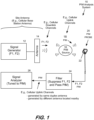
- FIG. 1 is conceptual illustration of a PIM analysis system 10.
- the PIM probe system represents an improved technique for precisely locating external PIM sources at an antenna broadcast site, such as a cellular telephone base station.
- the site antenna 14 is fed by a signal generator 12 producing high power test signals at frequencies F1 and F2.
- the test signals frequencies F1 and F2 and broadcast power level may correspond to the downlink channels used by a cellular telephone base station.
- the antenna 14 broadcasts the frequencies F1 and F2, which illuminate a PIM source 16.
- the PIM source creates harmonics and combines the incident energy creating PIM 18.
- the PIM source 16 may generate harmonics of the test frequencies F1 and F2, which may individually or in combination create PIM 18 corresponding to one or more uplink channels of the antenna 14.
- the test frequencies F1 and F2 may correspond to the downlink channels of a cellular base station antenna, while the PIM 18 frequencies or interest correspond to the uplink channels of that same cellular base station antenna.
- the improved PIM detection technique involves using a near field PIM probe 20 with a PIM antenna 22 connected to a signal analyzer 26 to "interference hunt" for PIM sources beyond the antenna.
- An illustrative test configuration is shown in FIG. 1 (see also FIG. 10 ).
- two high power test signals F1 and F2 are transmitted into the environment around the site antenna 14.
- F1 and F2 high power test signals
- F1 and F2 high power test signals
- a number of transmitters may be used to evaluate a prospective base station site prior to installing the antenna.
- a Remote Radio Head (RRH) at the site could be programmed to generate the two test signals or a traditional PIM analyzer could be used to generate the test signals.
- RRH Remote Radio Head
- a third option would be to develop a "transmit only" test device that is able to generate two test signals over a wide range of frequencies, with no provision for receiving the PIM signals produced.
- a fourth option utilizes a probe to detect broadband PIM. For example, a technician may not want to carry a PIM analyzer to the top of the tower to act as a signal source, and the RRH manufacturer may have not created software to generate two specific test tones. In this case, the technician may tune the PIM signal analyzer to a broad frequency range and use the cellular carrier frequency generated by the RRH as the signal source. The probe will detect broadband PIM frequencies in the same way. Rather than hunting for a single frequency (generated by specific F1 and F2), the technicians hunt for broadband noise rise corresponding to multiple F1 and F2 combinations generated by the individual cellular carrier resource block frequencies.
- the two test signals (F1 and F2) radiating from the antenna 14 mix at the PIM source 16 beyond the antenna and generate PIM 18 including intermodulation product frequencies (IM2, IM3, IM4, IM5, etc.) including various combinations of harmonics of F1 and F2.
- the PIM source 16 radiates these IM product frequencies (PIM 18) in all directions, enabling them to be detected using the PIM probe 20 connected to a remote receiver, such as the signal analyzer 26 by way of a filter 24 that suppresses the broadcast test signals (F1 and F2) and passes the PIM frequencies of interest.
- the filter may suppress the downlink channels of a duplex cellular base station antenna, and pass the uplink channels of that antenna.
- the receiver in this example is a signal analyzer 26 tuned to a known PIM product frequency created by the test frequencies (F1 and F2).
- the frequency span used is typically 100 kHz when narrow bandwidth CW signals are used for F1 and F2, as is the case when a PIM analyzer is used as the signal generator.
- a band-pass filter 24 may be attached to the signal analyzer to pass the PIM frequencies of interest and block the broadcast test signals (F1, F2) from entering the signal analyzer 26.
- a minimum of 30 dB rejection (attenuation) of the high power test signals (F1, F2) is typically sufficient. If the test signals (F1, F2) are able to enter the signal analyzer 26, they will generate active intermodulation products within the signal analyzer receiver, which can produce false readings.
- a low PIM test cable such as a coaxial cable, connects the filter and signal analyzer to the PIM probe.
- the PIM probe 20 should itself exhibit low PIM. If the PIM probe 20 generates PIM at a level close to the value the technician is trying to detect when exposing the probe to the high power test tones, everything beyond the antenna will falsely appear to be generating PIM. To combat this, the PIM probe 20 should be constructed with low PIM materials and all metal-to-metal connections should be soldered or designed to maintain high contact pressure.
- the PIM probe 20 can be used to take advantage of this fact by testing for significant PIM signal level increases when the PIM antenna 22 is positioned less than one wavelength from the PIM source. Inside this region, the PIM is directly coupling energy from the PIM source to the probe, experiencing significantly less path loss than when testing occurs more than one wavelength from the PIM source. At typical cellular telephone frequencies, this means that the PIM probe 20 works well when the PIM antenna 22 is placed within one wavelength (e.g., 6 to 18 inches at typical 1900 MHZ and 600 MHZ cellular frequencies, respectively) of the PIM source 16.
- the hand-held wand configuration assists the technician in placing the PIM antenna 22 close to structures to be tested, while standing out of the line of site between the antenna 14 and the structures being tested to the avoid blocking the RF beams radiated by the antenna 14.
- FIG. 2 is a perspective plan view of a PIM probe 20, which includes a PIM antenna 22 attached to one end of a wand 23 with a handle 25 attached to the other end of the wand.
- a coaxial cable 27 extends from the PIM antenna 22, through the hollow wand 23 and handle 25, and out of the handle 25.
- an internal cable may terminate at the handle, where a cable connecter is provided for connecting an auxiliary cable 27 to the probe.
- the auxiliary cable 27, connects to a filter 29 selected to pass the PIM frequencies of interest and suppress the test frequencies F1, F2 transmitted by the site antenna 14.
- the filter may suppress the downlink channels of a duplex cellular base station antenna, and pass the uplink channels of that antenna.
- Different filters may be selected to match different test frequencies and PIM frequencies of interest.
- the filter may be built into the wand of the PIM probe, in which case different probes may be selected to match different test frequencies.
- the filter may be built into a removable handle 25 of the PIM probe, in which case different handles may be selected and installed on the wand to match different test frequencies.
- FIG. 3 is a perspective plan view of the PIM antenna 22, which has a PC board printed conductor configuration including conductor rings printed on two orthogonal PC boards. More specifically, the PIM antenna 22 includes a first PC board forming vane-1 30 carrying a ring shaped printed conductor trace-1 32. A second PC board forming second vane-2 34, positioned orthogonal to vane-1, carries a second ring shaped printed conductor trace-2 36. The PC board vanes interlock without electrically connecting the traces. A first end of each trace attaches to the center conductor of the coaxial cable, while the other end attaches to the mesh ground shield conductor of the coaxial cable.
- the PIM antenna 22 is a magnetic field antenna largely circular in shape having an outside diameter of 1.25 inch and an inside diameter of 1.0 inch. One end of the loop is soldered to the center conductor of the feeding coaxial cable and the other end is soldered to the ground shield of the cable.
- the PIM antenna is tuned by loop size to receive the PIM frequencies of interest, typically corresponding to the uplink channels of the site antenna.
- the circumference of the inner and outer diameters may be close to being resonant (multiples of 1 ⁇ 4 wavelength) of the uplink frequencies of the commercial wireless bands in the 700 MHz to 2600 MHz range.
- Antennas with different loop sizes may be tuned by loop size selection at multiples of 1 ⁇ 4 wavelength of specific PIM frequencies of interest.
- FIG. 4 is a perspective view of an illustrative PIM probe 40 shown approximately to scale.
- the PIM antenna is under an antenna cover 41 formed of material impervious to RF radiation, such as rubber or plastic.
- a wand 42 approximately three feet long extends from the antenna cover 41 to the handle 43.
- a coaxial cable 44 extends from the handle.
- the PIM antenna under the cover 41 may be soldered directly to an internal coaxial cable to minimize PIM creation at the connection.
- a removable antenna with cover in place may thread or fit into a connector on the end of the wand 42 allowing for the PIM antenna to be removed and replaced as desired.
- a coaxial cable connector at the end of the handle 43 may also be soldered directly to the internal coaxial cable to minimize PIM creation at the connection.
- a filter may be disposed in the handle 43, which may thread or fit into a connector on the end of the wand 42 allowing for the PIM antenna to be removed and replaced as desired.
- FIG. 5A is a front view of vane-1 30 of the PC board type of PIM probe antenna 22.
- Vane-1 30 carries a first ring trace-1 32 that is open at the bottom forming an open rather than a closed ring.
- a hole 52 surrounded by a trace buffer 53 at the apex of the trace-1 32 and a slot 54 slot are provided for receiving the other vane-2 34 (shown in FIG. 5B ).
- a conductive pin 57 (shown in FIG. 5B ) extends through the hole 52 where it bridges the trace-2 36 on vane-2 34 without electrically connecting to trace-1 32 on vane-1 30.
- the trace buffer 53 is an area of the PC board not covered by the trace-1 32 allowing the pin 57 to pass through the hole 52 without electrically contacting the trace-1.
- a wire with an insulator cover could be utilized instead of the trace buffer 53 to allow the conductive bridge to pass through the hole 52 without electrically contacting the trace-1.
- FIG. 5B is a front view of vane-2 34 of the PC board type of PIM probe antenna 22.
- Vane-2 34 carries a second ring trace-2 36 that is open at the bottom forming an open rather than a closed ring.
- a slot 56 at the apex of the trace-2 36 is provided for receiving the other vane-1 30 (shown in FIG. 5A ).
- the pin 57 extends through the hole 52 in the vane-1 30 where it bridges the slot 56 on vane-2 34 to provide electrical continuity of the trace-2 36 across the slot 56 without electrically connecting to trace-1 32 on the other vane-1 30.
- the trace buffer 53 allows the pin 57 to pass through the hole 52 and bridge the trace-2 36 across the slot 56 without electrically contacting the trace-1 32 on vane-1 30 (shown in FIG. 5A ).
- FIG. 6A shows that the center conductor of the coaxial cable forms a first center conductor connection 35A with one end of trace-1 32, while the coaxial cable ground conductor forms a first ground conductor connection 37A with the other end of trace-1 32 on vane-1 30.
- FIG. 6B shows that the center conductor of the coaxial cable forms a second center conductor connection 35B with one end of trace-2 36, while the coaxial cable ground conductor forms a second ground conductor connection 37B with the other end of trace-2 36 on vane-2 34.
- FIG. 7 is a perspective plan view of a wire loop type of PIM probe 72.
- This probe is similar to the PIM probe 20, except that the PC board vanes are replaced by wire loop-1 72A and wire loop-2 72B typically located inside a protective cover.
- a section of electric insulator 74 prevents the wire loops from electrically contacting each other.
- FIG. 8 shown for wire loop-1 72A which is essentially the same for both wire loops, shows that the coaxial cable makes a center loop connection 82A with one end of the wire loop-1 72A, and a ground conductor connection 84A with the other end of the loop.
- the outside diameter of each wire loop may be approximately 1.25 inch. While the material cost of the wire loops is very low, they are difficult to assemble by hand.
- the alternative PC board type of antenna utilizes more expensive printed circuit loops to greatly simplify assembly.
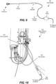
- FIG. 9 is a conceptual illustration of wire loop type of PIM probe 90, which includes a PIM antenna 92 attached to one end of a wand 93 with a handle 95 attached to the other end of the wand.
- a coaxial cable 97 extends from the PIM antenna 92, through the hollow wand 93 and handle 95, and out of the handle 95.
- an internal cable may terminate at the handle, where a cable connecter is provided for connecting an auxiliary cable 97 to the probe.
- the auxiliary cable 97 connects to a filter 99 selected to suppress the test frequencies F1, F2 transmitted by the site antenna and passes the PIM frequencies of interest. Different filters may be selected to match different test frequencies and different PIM frequencies of interest.
- the filter may be built into the PIM probe 90, in which case different probes having different loop diameters may be selected to match different test frequencies and PIM frequencies of interest.
- the filter may be built into a removable handle 95 of the PIM probe, in which case different handles may be selected and installed on the wand to match different test frequencies.
- FIG. 10 is a conceptual illustration of a PIM probe 100 shown approximately to scale used to measure PIM at the site of a cellular base station antenna 102.
- the PIM antenna end of the probe may be positioned by hand very close to a suspected PIM source 104.
- the PIM antenna end of the probe may be positioned within one wavelength of the PIM frequencies of interest, such as the uplink frequencies of the antenna 102, typically one wavelength (e.g., 6 to 18 inches at typical 1900 MHZ and 600 MHZ cellular frequencies, respectively).
- the size and shape of the PIM probe 100 allows the technician to position the PIM antenna end of the probe with one hand while standing out of the line of site from the antenna 102 to the PIM antenna of the probe 100.
- a filter 106 in line from the probe to a signal analyzer suppresses the downlink broadcast frequencies of the antenna 102 and passes the PIM frequencies of interest.
- the length of the probe is 35 inches from tip of input connector to top of the protective cover of the probe. This minimum length is advantageous to keep the technician's body out of the line between the site antenna and the PIM source.
- the human body has typically 10 dB RF isolation. If the technician's body comes between the site antenna and the PIM source, the magnitude of PIM produced by the source will reduce by as much as 40 dB.
- the probe should have a rugged design.
- the handle may be a rubberized grip on one end of the wand.
- the antenna cover may be an injection molded plastic or rubberized housing (also known as a radome) protecting the PIM antenna.
- an injection molded cover may be manufactured from high impact strength ABS plastic to protect the inner printed PC board or wire loop antenna.
- the wand may be a filament wound fiberglass tube connecting the grip to the cover.
- the RF connector on the grip end may be manufactured from stainless steel for maximum mate/de-mate life.
Landscapes
- Physics & Mathematics (AREA)
- Electromagnetism (AREA)
- General Physics & Mathematics (AREA)
- Engineering & Computer Science (AREA)
- Computer Networks & Wireless Communication (AREA)
- Signal Processing (AREA)
- Monitoring And Testing Of Transmission In General (AREA)
- Mobile Radio Communication Systems (AREA)
Claims (11)
- Passive-Intermodulation-Prüfsystem, PIM-Prüfsystem (10), das Folgendes umfasst:eine PIM-Antenne (22), die ausgebildet ist, um durch eine Schleifengröße abgestimmt zu werden, um Hochfrequenzsignale zu empfangen, die die PIM-Frequenz (18) von Interesse, die durch eine oder mehrere ausgesendete Frequenzen einer Standortantenne generiert wird, umfassen, wobei die PIM-Antenne (22) eine Rahmenantenne ist,einen Stab (23), der ausgebildet ist, um die PIM-Antenne (22) auf einem Ende zu tragen, und zu einer händischen Positionierung der PIM-Antenne (22) ausgebildet ist,ein Koaxialkabel (27), das ausgebildet ist, um elektrisch mit der PIM-Antenne (22) verbunden zu werden, und sich von ihr weg erstreckt;ein Filter (29), das ausgebildet ist, um mit dem Koaxialkabel verbindbar zu sein und die ausgesendeten Frequenzen zu unterdrücken und die PIM-Frequenzen von Interesse passieren zu lassen; undeinen Signalanalysator, der ausgebildet ist, um mit dem Koaxialkabel (27) verbindbar zu sein und eine Darstellung der PIM, die durch die PIM-Antenne empfangen wird, anzuzeigen;wobei die PIM-Antenne (22) eine Nahfeld-Magnetfeldantenne umfasst, die betriebsfähig ist, um ein von der Standortantenne ausgesendetes Signal von einer PIM-Störquelle zu detektieren, wobei die PIM-Störquelle durch eine Wellenlänge gekennzeichnet ist, indem die PIM-Antenne (22) innerhalb einer Wellenlänge der PIM-Störquelle platziert wird, und wobei der Signalanalysator ausgebildet ist, um die PIM-Störquelle basierend auf der Stärke des detektierten Signals zu lokalisieren.
- PIM-Prüfsystem (10) nach Anspruch 1, wobei die PIM-Antenne (22) zwei orthogonale Flügel mit auf Leiterplatten gedruckten Leitern umfasst.
- PIM-Prüfsystem (10) nach Anspruch 1, wobei die PIM-Antenne (22) zwei orthogonale Drahtschleifen umfasst.
- PIM-Prüfsystem (10) nach Anspruch 1, wobei sich das Koaxialkabel (27) durch den Stab erstreckt.
- PIM-Prüfsystem (10) nach Anspruch 1, das ferner einen Griff an dem zu der PIM-Antenne entgegengesetzten Ende des Stabs umfasst, wobei sich das Koaxialkabel von der PIM-Antenne (22) durch den Stab und durch den Griff erstreckt.
- PIM-Prüfsystem (10) nach Anspruch 1, wobei das Filter (29) innerhalb des Griffs oder innerhalb des Stabs positioniert ist.
- PIM-Prüfsystem (10) nach Anspruch 1, das ferner eine Schutzabdeckung über der PIM-Antenne umfasst.
- PIM-Prüfsystem (10) nach Anspruch 1, wobei das Filter (29) mit dem Koaxialkabel zwischen dem Stab und dem Signalanalysator in Reihe positioniert ist.
- PIM-Prüfsystem (10) nach Anspruch 1, wobei die PIM-Antenne (22) eine Drahtschleife umfasst.
- PIM-Prüfsystem (10) nach Anspruch 1, wobei die PIM-Antenne (22) eine einzige Schleife umfasst.
- PIM-Prüfsystem (10) nach Anspruch 1, wobei die PIM-Antenne (22) eine Leiterbahnschleife umfasst.
Applications Claiming Priority (2)
| Application Number | Priority Date | Filing Date | Title |
|---|---|---|---|
| US201662400117P | 2016-09-27 | 2016-09-27 | |
| PCT/US2017/053213 WO2018063977A1 (en) | 2016-09-27 | 2017-09-25 | Passive intermodulation (pim) probe |
Publications (4)
| Publication Number | Publication Date |
|---|---|
| EP3520171A1 EP3520171A1 (de) | 2019-08-07 |
| EP3520171A4 EP3520171A4 (de) | 2020-05-13 |
| EP3520171B1 true EP3520171B1 (de) | 2024-08-28 |
| EP3520171C0 EP3520171C0 (de) | 2024-08-28 |
Family
ID=61685267
Family Applications (1)
| Application Number | Title | Priority Date | Filing Date |
|---|---|---|---|
| EP17857254.1A Active EP3520171B1 (de) | 2016-09-27 | 2017-09-25 | Sonde für passive intermodulation (pim) |
Country Status (4)
| Country | Link |
|---|---|
| US (1) | US10429423B2 (de) |
| EP (1) | EP3520171B1 (de) |
| AU (1) | AU2017338003B2 (de) |
| WO (1) | WO2018063977A1 (de) |
Families Citing this family (6)
| Publication number | Priority date | Publication date | Assignee | Title |
|---|---|---|---|---|
| US11646807B2 (en) * | 2019-08-21 | 2023-05-09 | Commscope Technologies Llc | Methods including detecting cables connected to ports of communications network equipment and related systems |
| CN112582788A (zh) * | 2019-09-30 | 2021-03-30 | 3M创新有限公司 | 用于无源互调减轻的磁性吸收器 |
| CN111521897A (zh) * | 2020-04-30 | 2020-08-11 | 华南师范大学 | 一种无源互调干扰源定位系统和定位测试方法 |
| CN114080022B (zh) * | 2020-08-20 | 2022-12-30 | 华为技术有限公司 | 一种无源互调源的定位方法及装置 |
| CN115604744A (zh) * | 2021-06-28 | 2023-01-13 | 华为技术有限公司(Cn) | 一种无源互调源数目确定方法及相关设备 |
| EP4497202A4 (de) | 2022-03-22 | 2026-03-04 | Concealfab Inc | Rf-absorber-pim-jagdsysteme |
Family Cites Families (14)
| Publication number | Priority date | Publication date | Assignee | Title |
|---|---|---|---|---|
| US4023093A (en) * | 1975-10-20 | 1977-05-10 | The Narda Microwave Corporation | Magnetic field radiation detector |
| DE3315210C2 (de) * | 1983-04-27 | 1986-04-10 | Institut für Rundfunktechnik GmbH, 8000 München | Nahfeldsonde zur Messung der drei magnetischen Komponenten einer elektromagnetischen Strahlung |
| WO2003030416A1 (en) * | 2001-10-01 | 2003-04-10 | Summitek Instruments, Inc. | Portable device used to measure passive intermodulation in radio frequency communication systems |
| CN102037528A (zh) * | 2008-03-20 | 2011-04-27 | 格瑞巴奇有限公司 | 屏蔽三端子平通emi/消能滤波器 |
| US20110260941A1 (en) * | 2008-10-15 | 2011-10-27 | Argus Technologies (Australia) Pty Ltd. | Wideband radiating elements |
| US9792408B2 (en) * | 2009-07-02 | 2017-10-17 | Covidien Lp | Method and apparatus to detect transponder tagged objects and to communicate with medical telemetry devices, for example during medical procedures |
| GB2510997B (en) * | 2012-05-21 | 2014-11-05 | Aceaxis Ltd | Detection of Intermodulation Products in a Wireless Network |
| US9291652B2 (en) | 2012-08-17 | 2016-03-22 | Cellco Partnership | Non-intrusive passive intermodulation testing |
| HK1217042A1 (zh) | 2013-03-15 | 2016-12-16 | Bird Technologies Group Inc. | 使用脉冲激励的无源互调测试 |
| US9728846B2 (en) * | 2013-08-09 | 2017-08-08 | Pulse Electronics, Inc. | Low passive intermodulation antenna apparatus and methods of use |
| GB2526787B (en) | 2014-05-29 | 2016-11-23 | Aceaxis Ltd | Processing of passive intermodulation detection results |
| US9337941B2 (en) * | 2014-06-20 | 2016-05-10 | The United States Of America As Represented By The Secretary Of The Navy | Antenna systems and methods for over-the-air transmitter signal measurement |
| US9392479B2 (en) | 2014-12-01 | 2016-07-12 | Fluke Corporation | Pocket-size PIM inspector |
| US10615885B2 (en) * | 2016-11-28 | 2020-04-07 | Johns Manville | Self-adhesive membrane for mitigating passive intermodulation |
-
2017
- 2017-09-07 US US15/698,606 patent/US10429423B2/en active Active
- 2017-09-25 EP EP17857254.1A patent/EP3520171B1/de active Active
- 2017-09-25 WO PCT/US2017/053213 patent/WO2018063977A1/en not_active Ceased
- 2017-09-25 AU AU2017338003A patent/AU2017338003B2/en active Active
Also Published As
| Publication number | Publication date |
|---|---|
| EP3520171A1 (de) | 2019-08-07 |
| US10429423B2 (en) | 2019-10-01 |
| AU2017338003B2 (en) | 2021-10-07 |
| US20180088161A1 (en) | 2018-03-29 |
| EP3520171A4 (de) | 2020-05-13 |
| EP3520171C0 (de) | 2024-08-28 |
| AU2017338003A1 (en) | 2019-04-18 |
| WO2018063977A1 (en) | 2018-04-05 |
Similar Documents
| Publication | Publication Date | Title |
|---|---|---|
| EP3520171B1 (de) | Sonde für passive intermodulation (pim) | |
| US9588212B1 (en) | Method of calibrating a measurement instrument for determining direction and distance to a source of passive intermodulation (PIM) | |
| CN110535540B (zh) | 测试被测装置的天线的消声测试室、测试系统及测试方法 | |
| US20160013565A1 (en) | Multi-band antenna assembly | |
| US7969367B2 (en) | Antenna coupler | |
| US7893685B2 (en) | RF meter with input noise suppression | |
| JP6179969B2 (ja) | 無線カバレッジが可能であるか否か判定するシステム | |
| Sakai et al. | Impact of emission noise and electromagnetic shielding on mobile communication systems in unmanned aerial vehicles | |
| US20200217879A1 (en) | System for testing wireless communication equipment employing antennas | |
| US6980163B2 (en) | Signal leakage detector | |
| US7170467B1 (en) | Antenna couplers and method of production | |
| CN102955086A (zh) | 一种波导转换开关屏蔽效能测试方法 | |
| Karlsson et al. | Co-site interference analysis and antenna system integration on a swedish combat vehicle platform | |
| US10763982B2 (en) | Method and system for over-the-air testing of unwanted emissions | |
| Moongilan | EIRP, TRP, Partial TRP and Radiated Immunity For 5G millimeter Wave Device Compliance | |
| JP2006220511A (ja) | 放射電磁界イミュニティ試験装置 | |
| JP2016176872A (ja) | 全電波無響室における不要輻射測定方法 | |
| Zhang et al. | Near Field Measurement: Characterizing System SNR against Frequency | |
| Hallon et al. | Testing EMC properties of electrical devices equipped wireless communication | |
| Cavallini et al. | Experience on measuring partial discharges in paper/oil medium-voltage distribution transformers | |
| Hallon et al. | Immunity against electromagnetic field testing of electrical devices using wireless communication | |
| CA1060984A (en) | Shielded antenna test coupler | |
| Venkatesulu et al. | Real Time Monitoring System For Electromagnetic Radiation Measurements Using Arm Processor For Cellular Base Stations | |
| Moongilan | Radiated immunity field uniformity enhancement techniques for milli-meter wave frequencies | |
| CN202916358U (zh) | 一种波导转换开关屏蔽效能测试装置 |
Legal Events
| Date | Code | Title | Description |
|---|---|---|---|
| STAA | Information on the status of an ep patent application or granted ep patent |
Free format text: STATUS: THE INTERNATIONAL PUBLICATION HAS BEEN MADE |
|
| PUAI | Public reference made under article 153(3) epc to a published international application that has entered the european phase |
Free format text: ORIGINAL CODE: 0009012 |
|
| STAA | Information on the status of an ep patent application or granted ep patent |
Free format text: STATUS: REQUEST FOR EXAMINATION WAS MADE |
|
| 17P | Request for examination filed |
Effective date: 20190329 |
|
| AK | Designated contracting states |
Kind code of ref document: A1 Designated state(s): AL AT BE BG CH CY CZ DE DK EE ES FI FR GB GR HR HU IE IS IT LI LT LU LV MC MK MT NL NO PL PT RO RS SE SI SK SM TR |
|
| AX | Request for extension of the european patent |
Extension state: BA ME |
|
| DAV | Request for validation of the european patent (deleted) | ||
| DAX | Request for extension of the european patent (deleted) | ||
| REG | Reference to a national code |
Ref country code: DE Ref legal event code: R079 Free format text: PREVIOUS MAIN CLASS: H01Q0005420000 Ipc: G01R0029080000 Ref document number: 602017084525 Country of ref document: DE |
|
| A4 | Supplementary search report drawn up and despatched |
Effective date: 20200417 |
|
| RIC1 | Information provided on ipc code assigned before grant |
Ipc: H04L 12/26 20060101ALN20200409BHEP Ipc: H01Q 1/38 20060101ALI20200409BHEP Ipc: H01Q 21/29 20060101ALI20200409BHEP Ipc: G01R 29/08 20060101AFI20200409BHEP Ipc: H01Q 5/30 20150101ALN20200409BHEP Ipc: H01Q 1/42 20060101ALN20200409BHEP Ipc: H01Q 7/00 20060101ALI20200409BHEP |
|
| STAA | Information on the status of an ep patent application or granted ep patent |
Free format text: STATUS: EXAMINATION IS IN PROGRESS |
|
| 17Q | First examination report despatched |
Effective date: 20230620 |
|
| GRAP | Despatch of communication of intention to grant a patent |
Free format text: ORIGINAL CODE: EPIDOSNIGR1 |
|
| STAA | Information on the status of an ep patent application or granted ep patent |
Free format text: STATUS: GRANT OF PATENT IS INTENDED |
|
| INTG | Intention to grant announced |
Effective date: 20240322 |
|
| RIC1 | Information provided on ipc code assigned before grant |
Ipc: G01R 29/08 20060101AFI20240308BHEP |
|
| GRAS | Grant fee paid |
Free format text: ORIGINAL CODE: EPIDOSNIGR3 |
|
| GRAA | (expected) grant |
Free format text: ORIGINAL CODE: 0009210 |
|
| STAA | Information on the status of an ep patent application or granted ep patent |
Free format text: STATUS: THE PATENT HAS BEEN GRANTED |
|
| AK | Designated contracting states |
Kind code of ref document: B1 Designated state(s): AL AT BE BG CH CY CZ DE DK EE ES FI FR GB GR HR HU IE IS IT LI LT LU LV MC MK MT NL NO PL PT RO RS SE SI SK SM TR |
|
| REG | Reference to a national code |
Ref country code: GB Ref legal event code: FG4D |
|
| REG | Reference to a national code |
Ref country code: CH Ref legal event code: EP |
|
| REG | Reference to a national code |
Ref country code: DE Ref legal event code: R096 Ref document number: 602017084525 Country of ref document: DE |
|
| REG | Reference to a national code |
Ref country code: IE Ref legal event code: FG4D |
|
| U01 | Request for unitary effect filed |
Effective date: 20240916 |
|
| U07 | Unitary effect registered |
Designated state(s): AT BE BG DE DK EE FI FR IT LT LU LV MT NL PT RO SE SI Effective date: 20241007 |
|
| U20 | Renewal fee for the european patent with unitary effect paid |
Year of fee payment: 8 Effective date: 20241001 |
|
| PG25 | Lapsed in a contracting state [announced via postgrant information from national office to epo] |
Ref country code: NO Free format text: LAPSE BECAUSE OF FAILURE TO SUBMIT A TRANSLATION OF THE DESCRIPTION OR TO PAY THE FEE WITHIN THE PRESCRIBED TIME-LIMIT Effective date: 20241128 |
|
| PG25 | Lapsed in a contracting state [announced via postgrant information from national office to epo] |
Ref country code: GR Free format text: LAPSE BECAUSE OF FAILURE TO SUBMIT A TRANSLATION OF THE DESCRIPTION OR TO PAY THE FEE WITHIN THE PRESCRIBED TIME-LIMIT Effective date: 20241129 Ref country code: PL Free format text: LAPSE BECAUSE OF FAILURE TO SUBMIT A TRANSLATION OF THE DESCRIPTION OR TO PAY THE FEE WITHIN THE PRESCRIBED TIME-LIMIT Effective date: 20240828 |
|
| PG25 | Lapsed in a contracting state [announced via postgrant information from national office to epo] |
Ref country code: IS Free format text: LAPSE BECAUSE OF FAILURE TO SUBMIT A TRANSLATION OF THE DESCRIPTION OR TO PAY THE FEE WITHIN THE PRESCRIBED TIME-LIMIT Effective date: 20241228 |
|
| PG25 | Lapsed in a contracting state [announced via postgrant information from national office to epo] |
Ref country code: HR Free format text: LAPSE BECAUSE OF FAILURE TO SUBMIT A TRANSLATION OF THE DESCRIPTION OR TO PAY THE FEE WITHIN THE PRESCRIBED TIME-LIMIT Effective date: 20240828 |
|
| PG25 | Lapsed in a contracting state [announced via postgrant information from national office to epo] |
Ref country code: ES Free format text: LAPSE BECAUSE OF FAILURE TO SUBMIT A TRANSLATION OF THE DESCRIPTION OR TO PAY THE FEE WITHIN THE PRESCRIBED TIME-LIMIT Effective date: 20240828 Ref country code: RS Free format text: LAPSE BECAUSE OF FAILURE TO SUBMIT A TRANSLATION OF THE DESCRIPTION OR TO PAY THE FEE WITHIN THE PRESCRIBED TIME-LIMIT Effective date: 20241128 |
|
| PG25 | Lapsed in a contracting state [announced via postgrant information from national office to epo] |
Ref country code: RS Free format text: LAPSE BECAUSE OF FAILURE TO SUBMIT A TRANSLATION OF THE DESCRIPTION OR TO PAY THE FEE WITHIN THE PRESCRIBED TIME-LIMIT Effective date: 20241128 Ref country code: PL Free format text: LAPSE BECAUSE OF FAILURE TO SUBMIT A TRANSLATION OF THE DESCRIPTION OR TO PAY THE FEE WITHIN THE PRESCRIBED TIME-LIMIT Effective date: 20240828 Ref country code: NO Free format text: LAPSE BECAUSE OF FAILURE TO SUBMIT A TRANSLATION OF THE DESCRIPTION OR TO PAY THE FEE WITHIN THE PRESCRIBED TIME-LIMIT Effective date: 20241128 Ref country code: IS Free format text: LAPSE BECAUSE OF FAILURE TO SUBMIT A TRANSLATION OF THE DESCRIPTION OR TO PAY THE FEE WITHIN THE PRESCRIBED TIME-LIMIT Effective date: 20241228 Ref country code: HR Free format text: LAPSE BECAUSE OF FAILURE TO SUBMIT A TRANSLATION OF THE DESCRIPTION OR TO PAY THE FEE WITHIN THE PRESCRIBED TIME-LIMIT Effective date: 20240828 Ref country code: GR Free format text: LAPSE BECAUSE OF FAILURE TO SUBMIT A TRANSLATION OF THE DESCRIPTION OR TO PAY THE FEE WITHIN THE PRESCRIBED TIME-LIMIT Effective date: 20241129 Ref country code: ES Free format text: LAPSE BECAUSE OF FAILURE TO SUBMIT A TRANSLATION OF THE DESCRIPTION OR TO PAY THE FEE WITHIN THE PRESCRIBED TIME-LIMIT Effective date: 20240828 |
|
| PG25 | Lapsed in a contracting state [announced via postgrant information from national office to epo] |
Ref country code: SM Free format text: LAPSE BECAUSE OF FAILURE TO SUBMIT A TRANSLATION OF THE DESCRIPTION OR TO PAY THE FEE WITHIN THE PRESCRIBED TIME-LIMIT Effective date: 20240828 |
|
| PG25 | Lapsed in a contracting state [announced via postgrant information from national office to epo] |
Ref country code: CZ Free format text: LAPSE BECAUSE OF FAILURE TO SUBMIT A TRANSLATION OF THE DESCRIPTION OR TO PAY THE FEE WITHIN THE PRESCRIBED TIME-LIMIT Effective date: 20240828 |
|
| PG25 | Lapsed in a contracting state [announced via postgrant information from national office to epo] |
Ref country code: SK Free format text: LAPSE BECAUSE OF FAILURE TO SUBMIT A TRANSLATION OF THE DESCRIPTION OR TO PAY THE FEE WITHIN THE PRESCRIBED TIME-LIMIT Effective date: 20240828 |
|
| REG | Reference to a national code |
Ref country code: CH Ref legal event code: PL |
|
| PLBE | No opposition filed within time limit |
Free format text: ORIGINAL CODE: 0009261 |
|
| STAA | Information on the status of an ep patent application or granted ep patent |
Free format text: STATUS: NO OPPOSITION FILED WITHIN TIME LIMIT |
|
| PG25 | Lapsed in a contracting state [announced via postgrant information from national office to epo] |
Ref country code: MC Free format text: LAPSE BECAUSE OF FAILURE TO SUBMIT A TRANSLATION OF THE DESCRIPTION OR TO PAY THE FEE WITHIN THE PRESCRIBED TIME-LIMIT Effective date: 20240828 |
|
| GBPC | Gb: european patent ceased through non-payment of renewal fee |
Effective date: 20241128 |
|
| PG25 | Lapsed in a contracting state [announced via postgrant information from national office to epo] |
Ref country code: CH Free format text: LAPSE BECAUSE OF NON-PAYMENT OF DUE FEES Effective date: 20240930 |
|
| PG25 | Lapsed in a contracting state [announced via postgrant information from national office to epo] |
Ref country code: IE Free format text: LAPSE BECAUSE OF NON-PAYMENT OF DUE FEES Effective date: 20240925 |
|
| 26N | No opposition filed |
Effective date: 20250530 |
|
| U20 | Renewal fee for the european patent with unitary effect paid |
Year of fee payment: 9 Effective date: 20250715 |
|
| PG25 | Lapsed in a contracting state [announced via postgrant information from national office to epo] |
Ref country code: GB Free format text: LAPSE BECAUSE OF NON-PAYMENT OF DUE FEES Effective date: 20241128 |
|
| PG25 | Lapsed in a contracting state [announced via postgrant information from national office to epo] |
Ref country code: CY Free format text: LAPSE BECAUSE OF FAILURE TO SUBMIT A TRANSLATION OF THE DESCRIPTION OR TO PAY THE FEE WITHIN THE PRESCRIBED TIME-LIMIT; INVALID AB INITIO Effective date: 20170925 |
|
| PG25 | Lapsed in a contracting state [announced via postgrant information from national office to epo] |
Ref country code: HU Free format text: LAPSE BECAUSE OF FAILURE TO SUBMIT A TRANSLATION OF THE DESCRIPTION OR TO PAY THE FEE WITHIN THE PRESCRIBED TIME-LIMIT; INVALID AB INITIO Effective date: 20170925 |