EP3520146B1 - Solarzellenvorrichtung und verfahren zur formung davon - Google Patents
Solarzellenvorrichtung und verfahren zur formung davon Download PDFInfo
- Publication number
- EP3520146B1 EP3520146B1 EP17781039.7A EP17781039A EP3520146B1 EP 3520146 B1 EP3520146 B1 EP 3520146B1 EP 17781039 A EP17781039 A EP 17781039A EP 3520146 B1 EP3520146 B1 EP 3520146B1
- Authority
- EP
- European Patent Office
- Prior art keywords
- type layer
- amorphous
- type
- layer
- dopants
- Prior art date
- Legal status (The legal status is an assumption and is not a legal conclusion. Google has not performed a legal analysis and makes no representation as to the accuracy of the status listed.)
- Active
Links
Images




Classifications
-
- H—ELECTRICITY
- H10—SEMICONDUCTOR DEVICES; ELECTRIC SOLID-STATE DEVICES NOT OTHERWISE PROVIDED FOR
- H10F—INORGANIC SEMICONDUCTOR DEVICES SENSITIVE TO INFRARED RADIATION, LIGHT, ELECTROMAGNETIC RADIATION OF SHORTER WAVELENGTH OR CORPUSCULAR RADIATION
- H10F77/00—Constructional details of devices covered by this subclass
- H10F77/10—Semiconductor bodies
- H10F77/16—Material structures, e.g. crystalline structures, film structures or crystal plane orientations
- H10F77/162—Non-monocrystalline materials, e.g. semiconductor particles embedded in insulating materials
- H10F77/164—Polycrystalline semiconductors
- H10F77/1642—Polycrystalline semiconductors including only Group IV materials
- H10F77/1645—Polycrystalline semiconductors including only Group IV materials including microcrystalline silicon
-
- C—CHEMISTRY; METALLURGY
- C23—COATING METALLIC MATERIAL; COATING MATERIAL WITH METALLIC MATERIAL; CHEMICAL SURFACE TREATMENT; DIFFUSION TREATMENT OF METALLIC MATERIAL; COATING BY VACUUM EVAPORATION, BY SPUTTERING, BY ION IMPLANTATION OR BY CHEMICAL VAPOUR DEPOSITION, IN GENERAL; INHIBITING CORROSION OF METALLIC MATERIAL OR INCRUSTATION IN GENERAL
- C23C—COATING METALLIC MATERIAL; COATING MATERIAL WITH METALLIC MATERIAL; SURFACE TREATMENT OF METALLIC MATERIAL BY DIFFUSION INTO THE SURFACE, BY CHEMICAL CONVERSION OR SUBSTITUTION; COATING BY VACUUM EVAPORATION, BY SPUTTERING, BY ION IMPLANTATION OR BY CHEMICAL VAPOUR DEPOSITION, IN GENERAL
- C23C16/00—Chemical coating by decomposition of gaseous compounds, without leaving reaction products of surface material in the coating, i.e. chemical vapour deposition [CVD] processes
- C23C16/02—Pretreatment of the material to be coated
- C23C16/0272—Deposition of sub-layers, e.g. to promote the adhesion of the main coating
- C23C16/029—Graded interfaces
-
- C—CHEMISTRY; METALLURGY
- C23—COATING METALLIC MATERIAL; COATING MATERIAL WITH METALLIC MATERIAL; CHEMICAL SURFACE TREATMENT; DIFFUSION TREATMENT OF METALLIC MATERIAL; COATING BY VACUUM EVAPORATION, BY SPUTTERING, BY ION IMPLANTATION OR BY CHEMICAL VAPOUR DEPOSITION, IN GENERAL; INHIBITING CORROSION OF METALLIC MATERIAL OR INCRUSTATION IN GENERAL
- C23C—COATING METALLIC MATERIAL; COATING MATERIAL WITH METALLIC MATERIAL; SURFACE TREATMENT OF METALLIC MATERIAL BY DIFFUSION INTO THE SURFACE, BY CHEMICAL CONVERSION OR SUBSTITUTION; COATING BY VACUUM EVAPORATION, BY SPUTTERING, BY ION IMPLANTATION OR BY CHEMICAL VAPOUR DEPOSITION, IN GENERAL
- C23C16/00—Chemical coating by decomposition of gaseous compounds, without leaving reaction products of surface material in the coating, i.e. chemical vapour deposition [CVD] processes
- C23C16/22—Chemical coating by decomposition of gaseous compounds, without leaving reaction products of surface material in the coating, i.e. chemical vapour deposition [CVD] processes characterised by the deposition of inorganic material, other than metallic material
- C23C16/24—Deposition of silicon only
-
- C—CHEMISTRY; METALLURGY
- C23—COATING METALLIC MATERIAL; COATING MATERIAL WITH METALLIC MATERIAL; CHEMICAL SURFACE TREATMENT; DIFFUSION TREATMENT OF METALLIC MATERIAL; COATING BY VACUUM EVAPORATION, BY SPUTTERING, BY ION IMPLANTATION OR BY CHEMICAL VAPOUR DEPOSITION, IN GENERAL; INHIBITING CORROSION OF METALLIC MATERIAL OR INCRUSTATION IN GENERAL
- C23C—COATING METALLIC MATERIAL; COATING MATERIAL WITH METALLIC MATERIAL; SURFACE TREATMENT OF METALLIC MATERIAL BY DIFFUSION INTO THE SURFACE, BY CHEMICAL CONVERSION OR SUBSTITUTION; COATING BY VACUUM EVAPORATION, BY SPUTTERING, BY ION IMPLANTATION OR BY CHEMICAL VAPOUR DEPOSITION, IN GENERAL
- C23C16/00—Chemical coating by decomposition of gaseous compounds, without leaving reaction products of surface material in the coating, i.e. chemical vapour deposition [CVD] processes
- C23C16/22—Chemical coating by decomposition of gaseous compounds, without leaving reaction products of surface material in the coating, i.e. chemical vapour deposition [CVD] processes characterised by the deposition of inorganic material, other than metallic material
- C23C16/30—Deposition of compounds, mixtures or solid solutions, e.g. borides, carbides, nitrides
- C23C16/32—Carbides
- C23C16/325—Silicon carbide
-
- C—CHEMISTRY; METALLURGY
- C23—COATING METALLIC MATERIAL; COATING MATERIAL WITH METALLIC MATERIAL; CHEMICAL SURFACE TREATMENT; DIFFUSION TREATMENT OF METALLIC MATERIAL; COATING BY VACUUM EVAPORATION, BY SPUTTERING, BY ION IMPLANTATION OR BY CHEMICAL VAPOUR DEPOSITION, IN GENERAL; INHIBITING CORROSION OF METALLIC MATERIAL OR INCRUSTATION IN GENERAL
- C23C—COATING METALLIC MATERIAL; COATING MATERIAL WITH METALLIC MATERIAL; SURFACE TREATMENT OF METALLIC MATERIAL BY DIFFUSION INTO THE SURFACE, BY CHEMICAL CONVERSION OR SUBSTITUTION; COATING BY VACUUM EVAPORATION, BY SPUTTERING, BY ION IMPLANTATION OR BY CHEMICAL VAPOUR DEPOSITION, IN GENERAL
- C23C16/00—Chemical coating by decomposition of gaseous compounds, without leaving reaction products of surface material in the coating, i.e. chemical vapour deposition [CVD] processes
- C23C16/22—Chemical coating by decomposition of gaseous compounds, without leaving reaction products of surface material in the coating, i.e. chemical vapour deposition [CVD] processes characterised by the deposition of inorganic material, other than metallic material
- C23C16/30—Deposition of compounds, mixtures or solid solutions, e.g. borides, carbides, nitrides
- C23C16/40—Oxides
- C23C16/407—Oxides of zinc, germanium, cadmium, indium, tin, thallium or bismuth
-
- H—ELECTRICITY
- H10—SEMICONDUCTOR DEVICES; ELECTRIC SOLID-STATE DEVICES NOT OTHERWISE PROVIDED FOR
- H10F—INORGANIC SEMICONDUCTOR DEVICES SENSITIVE TO INFRARED RADIATION, LIGHT, ELECTROMAGNETIC RADIATION OF SHORTER WAVELENGTH OR CORPUSCULAR RADIATION
- H10F10/00—Individual photovoltaic cells, e.g. solar cells
- H10F10/10—Individual photovoltaic cells, e.g. solar cells having potential barriers
- H10F10/13—Photovoltaic cells having absorbing layers comprising graded bandgaps
-
- H—ELECTRICITY
- H10—SEMICONDUCTOR DEVICES; ELECTRIC SOLID-STATE DEVICES NOT OTHERWISE PROVIDED FOR
- H10F—INORGANIC SEMICONDUCTOR DEVICES SENSITIVE TO INFRARED RADIATION, LIGHT, ELECTROMAGNETIC RADIATION OF SHORTER WAVELENGTH OR CORPUSCULAR RADIATION
- H10F10/00—Individual photovoltaic cells, e.g. solar cells
- H10F10/10—Individual photovoltaic cells, e.g. solar cells having potential barriers
- H10F10/17—Photovoltaic cells having only PIN junction potential barriers
-
- H—ELECTRICITY
- H10—SEMICONDUCTOR DEVICES; ELECTRIC SOLID-STATE DEVICES NOT OTHERWISE PROVIDED FOR
- H10F—INORGANIC SEMICONDUCTOR DEVICES SENSITIVE TO INFRARED RADIATION, LIGHT, ELECTROMAGNETIC RADIATION OF SHORTER WAVELENGTH OR CORPUSCULAR RADIATION
- H10F71/00—Manufacture or treatment of devices covered by this subclass
- H10F71/10—Manufacture or treatment of devices covered by this subclass the devices comprising amorphous semiconductor material
- H10F71/103—Manufacture or treatment of devices covered by this subclass the devices comprising amorphous semiconductor material including only Group IV materials
-
- H—ELECTRICITY
- H10—SEMICONDUCTOR DEVICES; ELECTRIC SOLID-STATE DEVICES NOT OTHERWISE PROVIDED FOR
- H10P—GENERIC PROCESSES OR APPARATUS FOR THE MANUFACTURE OR TREATMENT OF DEVICES COVERED BY CLASS H10
- H10P14/00—Formation of materials, e.g. in the shape of layers or pillars
- H10P14/20—Formation of materials, e.g. in the shape of layers or pillars of semiconductor materials
- H10P14/24—Formation of materials, e.g. in the shape of layers or pillars of semiconductor materials using chemical vapour deposition [CVD]
-
- H—ELECTRICITY
- H10—SEMICONDUCTOR DEVICES; ELECTRIC SOLID-STATE DEVICES NOT OTHERWISE PROVIDED FOR
- H10P—GENERIC PROCESSES OR APPARATUS FOR THE MANUFACTURE OR TREATMENT OF DEVICES COVERED BY CLASS H10
- H10P14/00—Formation of materials, e.g. in the shape of layers or pillars
- H10P14/20—Formation of materials, e.g. in the shape of layers or pillars of semiconductor materials
- H10P14/32—Formation of materials, e.g. in the shape of layers or pillars of semiconductor materials characterised by intermediate layers between substrates and deposited layers
- H10P14/3202—Materials thereof
- H10P14/3241—Materials thereof being conductive materials
-
- H—ELECTRICITY
- H10—SEMICONDUCTOR DEVICES; ELECTRIC SOLID-STATE DEVICES NOT OTHERWISE PROVIDED FOR
- H10P—GENERIC PROCESSES OR APPARATUS FOR THE MANUFACTURE OR TREATMENT OF DEVICES COVERED BY CLASS H10
- H10P14/00—Formation of materials, e.g. in the shape of layers or pillars
- H10P14/20—Formation of materials, e.g. in the shape of layers or pillars of semiconductor materials
- H10P14/34—Deposited materials, e.g. layers
- H10P14/3402—Deposited materials, e.g. layers characterised by the chemical composition
- H10P14/3404—Deposited materials, e.g. layers characterised by the chemical composition being Group IVA materials
- H10P14/3411—Silicon, silicon germanium or germanium
-
- H—ELECTRICITY
- H10—SEMICONDUCTOR DEVICES; ELECTRIC SOLID-STATE DEVICES NOT OTHERWISE PROVIDED FOR
- H10P—GENERIC PROCESSES OR APPARATUS FOR THE MANUFACTURE OR TREATMENT OF DEVICES COVERED BY CLASS H10
- H10P14/00—Formation of materials, e.g. in the shape of layers or pillars
- H10P14/20—Formation of materials, e.g. in the shape of layers or pillars of semiconductor materials
- H10P14/34—Deposited materials, e.g. layers
- H10P14/3438—Doping during depositing
- H10P14/3441—Conductivity type
- H10P14/3444—P-type
-
- H—ELECTRICITY
- H10—SEMICONDUCTOR DEVICES; ELECTRIC SOLID-STATE DEVICES NOT OTHERWISE PROVIDED FOR
- H10P—GENERIC PROCESSES OR APPARATUS FOR THE MANUFACTURE OR TREATMENT OF DEVICES COVERED BY CLASS H10
- H10P14/00—Formation of materials, e.g. in the shape of layers or pillars
- H10P14/20—Formation of materials, e.g. in the shape of layers or pillars of semiconductor materials
- H10P14/32—Formation of materials, e.g. in the shape of layers or pillars of semiconductor materials characterised by intermediate layers between substrates and deposited layers
- H10P14/3202—Materials thereof
- H10P14/3204—Materials thereof being Group IVA semiconducting materials
- H10P14/3211—Silicon, silicon germanium or germanium
-
- H—ELECTRICITY
- H10—SEMICONDUCTOR DEVICES; ELECTRIC SOLID-STATE DEVICES NOT OTHERWISE PROVIDED FOR
- H10P—GENERIC PROCESSES OR APPARATUS FOR THE MANUFACTURE OR TREATMENT OF DEVICES COVERED BY CLASS H10
- H10P14/00—Formation of materials, e.g. in the shape of layers or pillars
- H10P14/20—Formation of materials, e.g. in the shape of layers or pillars of semiconductor materials
- H10P14/34—Deposited materials, e.g. layers
- H10P14/3402—Deposited materials, e.g. layers characterised by the chemical composition
- H10P14/3404—Deposited materials, e.g. layers characterised by the chemical composition being Group IVA materials
- H10P14/3408—Silicon carbide
-
- Y—GENERAL TAGGING OF NEW TECHNOLOGICAL DEVELOPMENTS; GENERAL TAGGING OF CROSS-SECTIONAL TECHNOLOGIES SPANNING OVER SEVERAL SECTIONS OF THE IPC; TECHNICAL SUBJECTS COVERED BY FORMER USPC CROSS-REFERENCE ART COLLECTIONS [XRACs] AND DIGESTS
- Y02—TECHNOLOGIES OR APPLICATIONS FOR MITIGATION OR ADAPTATION AGAINST CLIMATE CHANGE
- Y02E—REDUCTION OF GREENHOUSE GAS [GHG] EMISSIONS, RELATED TO ENERGY GENERATION, TRANSMISSION OR DISTRIBUTION
- Y02E10/00—Energy generation through renewable energy sources
- Y02E10/50—Photovoltaic [PV] energy
- Y02E10/545—Microcrystalline silicon PV cells
-
- Y—GENERAL TAGGING OF NEW TECHNOLOGICAL DEVELOPMENTS; GENERAL TAGGING OF CROSS-SECTIONAL TECHNOLOGIES SPANNING OVER SEVERAL SECTIONS OF THE IPC; TECHNICAL SUBJECTS COVERED BY FORMER USPC CROSS-REFERENCE ART COLLECTIONS [XRACs] AND DIGESTS
- Y02—TECHNOLOGIES OR APPLICATIONS FOR MITIGATION OR ADAPTATION AGAINST CLIMATE CHANGE
- Y02E—REDUCTION OF GREENHOUSE GAS [GHG] EMISSIONS, RELATED TO ENERGY GENERATION, TRANSMISSION OR DISTRIBUTION
- Y02E10/00—Energy generation through renewable energy sources
- Y02E10/50—Photovoltaic [PV] energy
- Y02E10/548—Amorphous silicon PV cells
-
- Y—GENERAL TAGGING OF NEW TECHNOLOGICAL DEVELOPMENTS; GENERAL TAGGING OF CROSS-SECTIONAL TECHNOLOGIES SPANNING OVER SEVERAL SECTIONS OF THE IPC; TECHNICAL SUBJECTS COVERED BY FORMER USPC CROSS-REFERENCE ART COLLECTIONS [XRACs] AND DIGESTS
- Y02—TECHNOLOGIES OR APPLICATIONS FOR MITIGATION OR ADAPTATION AGAINST CLIMATE CHANGE
- Y02P—CLIMATE CHANGE MITIGATION TECHNOLOGIES IN THE PRODUCTION OR PROCESSING OF GOODS
- Y02P70/00—Climate change mitigation technologies in the production process for final industrial or consumer products
- Y02P70/50—Manufacturing or production processes characterised by the final manufactured product
Definitions
- the present invention relates to a solar cell apparatus of the type comprising a p-i-n structure and a method for forming the same.
- Solar cell apparatuses are largely diffused and world widely utilized as electrical devices capable of converting the energy of light directly into electricity by the photovoltaic effect.
- P-i-n structures based on doped silicon semiconductors and transparent conductive oxides (TCO) are typical and fundamental components of these devices comprising a p-type silicon based semiconductor region (e.g. p-type layer), a n-type silicon based semiconductor region (e.g. n-type layer) and a lightly doped "near" intrinsic silicon based semiconductor region (e.g. i-type layer).
- TCO is extremely important as front contact for thin film solar cells and its optical and electrical properties determine the correct behaviour of the device.
- p-i-n solar cells are typically designed in a certain configuration where the p-type silicon is in direct electric contact with the front TCO. It is known that p-i-n cells use a textured TCO (e.g. tin dioxide (SnO 2 )) front contact that has suitable transmittance and electrical properties even though susceptible to reduction by hydrogen during the Plasma Enhanced Chemical Vapour Deposition (PECVD).
- PECVD Plasma Enhanced Chemical Vapour Deposition
- ZnO zinc oxide
- PVD Physical Vapour Deposition
- CVD Chemical Vapour Deposition
- a p-i-n type solar cells with ZnO as TCO is disclosed in US 2013/0048987 , relating to a method for forming a p-i-n structure on a substrate including forming a bi-layer p-type layer on the substrate by: depositing a microcrystalline p-type layer over the protective layer; and depositing an amorphous p-type layer over the microcrystalline p-type layer; depositing an amorphous i-type layer via hot wire chemical vapour deposition over the amorphous p-type layer; and depositing an amorphous n-type layer over the amorphous i-type layer.
- the p-i-n structure includes a bi-layer p-type layer disposed above a substrate, the bi-layer p-type layer having a microcrystalline p-type layer and an amorphous p-type layer disposed over the microcrystalline p-type layer; an amorphous i-type layer disposed over the bi-layer p-type layer; and an n-type layer disposed over the i-type layer.
- a p-i-n type solar cell with ZnO as a transparent conductive oxide layer are disclosed in WO 2011/033072 A2 and US 2010/307574 A1 .
- the higher haze properties and good transmittance of ZnO allow the solar cell to capture more light inside its absorber layers.
- the fabrication of p-i-n type solar cells with ZnO as TCO results in a lower fill factor (FF) and significantly lower open circuit voltage (Voc).
- FF fill factor
- Voc open circuit voltage
- the aim of the invention is to provide a solar cell apparatus and a method for forming the same that overcomes the drawbacks of known solar cell apparatuses.
- a further object of the invention is providing a solar cell apparatus in which the n-doped TCO/p-Si work function mismatch is reduced, significantly improving the solar cell performances.
- Another object of the invention is to overcome the problem of low work function TCOs, including the fabrication of p-type transparent conducting oxide layers.
- a further object of the invention is to provide a solar cell apparatus in which it is possible to fully take advantage of the better optical properties of TCO materials like the ZnO, without reducing the carrier conduction at the interface.
- Still another object of the invention is to provide a method for forming a solar cell apparatus which is suitable for large area photovoltaic modules applications.
- the solar cell apparatus of the present invention provides a reduced work function mismatch and reduction of the depletion layer of at the ZnO/p-SiC interface.
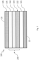
- the solar cell apparatus 100 comprises a substrate 101, preferably produced with ceramic or metallic or polymeric or composite materials or the like.
- the substrate 101 identifies a first end 10 of the solar cell apparatus 100 over which further layers are realized.
- the substrate 101 can be deposited via Chemical Vapour Deposition (CVD) methods.
- CVD Chemical Vapour Deposition
- the solar cell apparatus comprises an n-type transparent conductive oxide (TCO) layer 102 and a p-i-n structure 200.
- TCO transparent conductive oxide
- the p-i-n structure 200 comprises a p-type layer 103, an i-type layer 104, an n-type layer 105.
- a metal back layer 106 is arranged on the p-i-n structure 200 and defines a second end 20 of the solar cell apparatus 100 opposite to the first end 10.
- the n-type transparent conductive oxide (TCO) layer 102, the p-i-n structure 200 and the metal back layer 106 are sequentially deposited over the substrate 101.
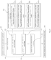
- the above layers are preferably deposited via PECVD in accordance with some embodiments of the present invention, by means of a method globally represented with the reference number 400.
- the method 400 is performed on the substrate 101 over which further layers or regions of materials are deposited.
- the substrate 101 is made of any suitable material to support and enhance a p-i-n junction and therefore to positively collaborate in generating the solar cell apparatus 100.
- the method 400 generally begins at 402 wherein the n-type transparent conductive oxide (TCO) layer 102 is deposited over the substrate 101, preferably via Plasma Enhanced Chemical Vapour deposition (PECVD).
- TCO transparent conductive oxide
- PECVD Plasma Enhanced Chemical Vapour deposition
- the n-type transparent conductive oxide (TCO) layer 102 comprises any material suitable to provide electrical conductivity together with sufficient transparency for the equipment.
- the n-type transparent conductive oxide (TCO) layer 102 comprises cadmium stannate (Cd 2 SnO 4 ), tin oxide (SnO), tin dioxide (SnO 2 ), combination thereof such as indium-tin oxide (ITO) or the like.
- the n-type transparent conductive oxide (TCO) is zinc oxide (ZnO).
- the n-type transparent conductive oxide (TCO) layer 102 comprises, in some embodiments, further dopants such as boron (B) gallium (Ga), aluminum (Al), tin (Sn).
- the deposition is obtained by a PECVD equipment 600.
- the PECVD process offers the intrinsic benefit to have the possibility to produce at the previous phase 402 of the method 400 an as-grown textured n-type transparent conductive oxide (TCO) layer 102, improving light absorption by enhancing light trapping within it.
- TCO transparent conductive oxide
- by tuning the deposition conditions of the method 400 achieved by using the PECVD equipment 600, and depositing ZnO as the n-type transparent conductive oxide (TCO) layer 102 it is possible to control the optical haze properties (where haze is the ratio between diffused and total transmittance through the TCO) up to values higher than 40% at a wavelength of 550nm with respect to the prior art.
- Typical crystallographic structure of ZnO:B TCO's for a-Si cells application X-ray diffraction spectrum shows a strong preferential crystallographic orientation, within the (11 2 0) plane parallel to the surface.
- the peaks positions observed for Low Pressure Chemical Vapour Deposition (LPCVD) ZnO:B concur with the literature for ZnO layers that crystallize in the hexagonal wurtzite (B4 type) structure and fit in the space group.
- the preferential crystallographic growth axis is within the plane (11 2 0), parallel to the substrate.
- This preferential orientation is typical for ZnO film growth by LPCVD [Wenas 1991, Fa ⁇ 2005] in the range of temperatures (i.e. 150 °C -200 °C) that produce films with a rough surface, suitable for thin film solar cells applications.
- the structure is composed of two interpenetrating hexagonal close packed sub-lattices; zinc atoms are surrounded by four oxygen atoms that form a tetrahedral pyramid, and vice versa.
- This tetrahedral coordination corresponds to a sp3 covalent bond, but this material also has a strong ionic character [Jagadish 2006]. Due to the non-symmetry of the [0002] and [0002] directions, this structure shows two possible polarities along the c axis (see fig. 8 and 9 ).
- the p-i-n structure 200 comprising the p-type layer 103, the i-type layer 104 and the n-type layer 105 is deposited at 500 of the method 400 on the n-type transparent conductive oxide (TCO) layer 102 preferably via PECVD.
- TCO transparent conductive oxide
- the p-type layer 103 is produced accordingly in step 403 of the method 400.
- the p-type layer 103 is produced with either SiC or SiOx or SixNy or a combination thereof.
- Si, SiC or SiOx are amorphous hydrogenated layers. It should be noted that SiC, SiOx or SixNy are advantageously used because of their higher energy gaps that ensure high transmittance of photons with energy close to the a-Si:H energy gap.
- the fabrication of the p-i-n structure 200 with single (a-Si:H) or double junctions (a-Si:H/ ⁇ c-Si:H) solar cell apparatus 100 on ZnO as the n-type transparent conductive oxide (TCO) layer 102 results in a lower fill factor (FF) and significantly lower open circuit voltage (Voc).
- FF fill factor
- Voc open circuit voltage
- a rectifying contact is formed between the p-type layer 103 and the ZnO n-type transparent conductive oxide (TCO) layer 102 because ZnO work-function is significantly lower than that of the p-type layer 103: ZnO work function is of about 4.65eV whereas that of amorphous Si, generally comprised in the p-type layer 103, is 4.9eV or even higher. Differently, the work function of SnO 2 TCO is of about 4.9eV, i.e. well aligned with the p-type layer 103 silicon based semiconductor (or SiC or SiOx or SixNy based).
- the p-type layer comprises amorphous, nanocrystalline or microcrystalline structures or combination thereof with the possibility of manifesting different levels of dopants concentrations within to enhance charge collection.
- the nanocrystalline silicon layer as interface layer has a significantly lower resistivity than p-type amorphous silicon based layer (a-Si:H, a-SiC:H, a-SixNy:H or a-SiOx:H) and very good optical properties.
- the thin interfacial layer is deposited between the n-type TCO film and the p-type a-SiC:H layer (or a-SiN:H or a-SiOx:H) and tuning the thicknesses and the gas ratios with multideposition steps to obtain a right trade-off between increased light absorption, which leads to a higher short circuit current (Isc), and improved FF and Voc, thanks to the reduced band-offset and better work-function matching,
- the Silane concentration (SiH4/(H2+SiH4) ) ratio is properly chosen to minimize the incubation time due to H2 induced ZnO surface modification, thus avoiding the formation of low density nucleation micro or nano-crystallites and to have fully coalesced micro-or nano crystalline phase and not amorphous or mixed phases.
- Deposition rate of the interface layer plays also an important role. In fact, a too slow growth could fail to protect the TCO from H2 induced accumulation layer which increases the depletion zone. This is controlled and regulated by SiH4 flow and RF power.
- dopants comprised in the p-type layer 103 are, for example, elements of the Group III such as boron (B), aluminum (Al), gallium (Ga) and combination thereof. Further preferably, precursors gas containing B are used due to their characteristic of being easier and safer to be used and handle than Al or Ga ones during plasma deposition processes.
- n-type transparent conductive oxide (TCO) layer 102 preferably ZnO based
- the p-type layer 103 to increase the Voc due to the increased junction built-in (V bi ) potential a thin and highly doped p-type layer comprising a nanocrystalline phase is produced allowing to reduce the n-type transparent conductive oxide (TCO) layer 102 (preferably ZnO based)/ p-type layer 103 Si based work function mismatch, significantly improving the solar cell apparatus 100 performances.
- the p-type layer 103 comprises a p-type dopants graded multi-layers structure 3 having a dopants concentration profile that varies as a function of thickness of said structure 3, thus allowing to gain smooth potential drops as a function of varying thickness.
- TCO transparent conductive oxide
- Fig. 2 is a sectional view comprising, at an enlarged scale, the detailed sequence of the p-type dopants graded multi-layers structure 3.
- a first nanocrystalline or microcrystalline p-type layer 3a is deposited over the n-type transparent conductive oxide (TCO) layer 102.
- TCO transparent conductive oxide
- the first nanocrystalline or microcrystalline p-type layer 3a is chosen with a specific architectural crystallographic lattice structure having a significantly lower electrical resistivity than an equivalent p-type layer 103 silicon based with an amorphous crystallographic structure together with very good optical properties.
- the process parameters of the PECVD equipment 600 are advantageously finely controlled, monitored and tuned.
- a H 2 /SiH 4 ratio low enough to minimize the incubation time due to H 2 induced ZnO surface modification is advantageously defined.
- Preferred values of SiH 4 /(SiH 4 + H 2 ) or H 2 /SiH 4 are around 0.5% and B 2 H 6 /(SiH 4 + B 2 H 6 ) around 8%.
- a second amorphous p-type layer 3b comprises silicon (Si), silicon and hydrogen (Si-H) or the like.
- the deposition rate used during 303a for depositing the first nanocrystalline or microcrystalline p-type layer 3a with a designed dopant concentration are sufficiently high to lessen H 2 induced accumulation layer which increases the depletion zone: this process feature is ruled by the SiH 4 flow set at 0,36 slm and the Plasma generator device power set at 0,1 W/cm 2 .
- the dopant is a boron compound
- precursor comprising trimethylboron (B(CH 3 ) 3 or TMB), diborane (BH 3 ) 2 , borontrifluoride (BF 3 ), triethylboron (B(C 2 H 5 ) 3 or TEB) or the like are advantageously used.
- B 2 H 6 or TMB flows must be controlled in the range of 0 to 100 sccm with the SiH 4 flow is constructively set at 5 slm and H 2 at 100 slm.
- the B 2 H 6 or TMB flow must be controlled in the range of 0 to 100 sccm when SiH 4 is varied from 0 to 5 slm and H 2 from 0 to 100 slm.
- Other type of dopants such as arsenic could be used to actively dope the p-type layer though the use of boron turns out to be more viable when associated with the PECVD techniques.
- an optimal range for boron doping concentration in the first nanocrystalline or microcrystalline p-type layer 3a is between 1E19 and 5E20 at/cm 3 .
- the B 2 H 6 /SiH 4 ratio in the range between 1E-2 and 1E-4 must be used for optimal performances with the desired crystallographic structures.
- the thickness of the first nanocrystalline or microcrystalline p-type layer 3a is formed with a first dopant concentration.
- the range of thickness of the first nanocrystalline or microcrystalline p-type layer 3a produced according to 303a is between 3 and 10 nm with a deposition time lower than 30 sec (giving a deposition growth rate of about 6 nm/min to 20 nm/min). This allows a good trade-off between light transmission and electrical performances. Above those thicknesses light absorption by the nano-crystalline layer will have a significant impact on Tandem cell Current density (Jsc) and on the series resistance of the monolithically connected cells, below such values the work function alignment improvement will be lost.
- Jsc Tandem cell Current density
- an optimal thickness value of the first nanocrystalline or microcrystalline p-type layer 3a is around 7nm. It is important to underline that above these thickness values light absorption by the first nanocrystalline or microcrystalline p-type layer 3a decreases with the reduction of the tandem cell current density (Jsc) and with the increase of the series resistance of the solar cell apparatus 100, while below these thickness values the work function alignment improvement between the first nanocrystalline or microcrystalline p-type layer 3a silicon based and the n-type transparent conductive oxide (TCO) layer 102 silicon based is mainly lost.
- the deposition temperatures at the 303a are in the range of almost 150 and 190 °C.
- a second amorphous p-type layer 3b with a second dopant concentration is deposited over the first nanocrystalline or microcrystalline p-type layer 3a as shown in details in Fig. 2 .
- the first nanocrystalline or microcrystalline p-type layer 3a represents an interface structure interposed between the TCO and the second amorphous p-type layer 3b.
- the second amorphous p-type layer 3b comprises any material suitable to produce the necessary features to form the p-i-n structure 200.
- the second amorphous p-type layer 3b comprises silicon (Si), silicon carbide (SiC) or the like.
- dopants concentration within the second amorphous p-type layer 3b is varied with respect to the one of the first nanocrystalline or microcrystalline p-type layer 3a.
- suitable values of SiH 4 /(SiH 4 + H 2 ) or H 2 /SiH 4 are around 5% and B 2 H 6 /(SiH 4 + B 2 H 6 ) around 6% .
- the second amorphous p-type layer 3b shows a dopants concentration gradient as a function of its thickness.
- the dopant is a boron compound
- a boron compound advantageously are used precursor comprising trimethylboron (B(CH 3 ) 3 or TMB), diborane (BH 3 ) 2 , borontrifluoride (BF 3 ), triethylboron (B(C 2 H 5 ) 3 or TEB) or the like.
- B 2 H 6 flows is preferably controlled in the range of 2-10 %.
- an advantageous range for boron doping concentration in the second amorphous p-type layer 3b is between 5 and 8 %.
- B 2 H 6 is used as the precursor gas 30 - 60 sccm generates the desired crystallographic structures.
- the second amorphous p-type layer 3b has a thickness in the range of 3-10 nm, with an advantageous thickness of almost 6 nm, having a deposition rate similar to the one used to produce the first nanocrystalline or microcrystalline p-type layer 3a (i.e. between 6 nm/min and 20 nm/min). Crystallites dimensions in the second amorphous p-type layer 3b result significantly reduced with respect to those contained in the first nanocrystalline or microcrystalline p-type layer 3a as a consequence of a SiH 4 /(SiH 4 +H 2 ) flow increase within the PECVD reactor.
- Typical deposition temperatures at the step 303b are in the range of 160 and 200°C.
- a third amorphous p-type layer 3c with a third dopant concentration is deposited over the second amorphous p-type layer 3b as shown in details in figure 2 .
- the third amorphous p-type layer 3c comprises any material suitable to produce the necessary features to form the p-i-n structure 200.
- the third amorphous p-type layer 3c comprises silicon (Si), silicon carbide (SiC) or the like.
- dopants concentration within the third amorphous p-type layer 3c is varied with respect to the one of the second amorphous p-type layer 3b.
- suitable values of SiH 4 /(SiH 4 + H 2 ) are around 9% and B 2 H 6 /(SiH 4 + B 2 H 6 ) around 4.8%.
- the dopant is a boron compound
- precursor comprising trimethylboron (B(CH 3 ) 3 or TMB), diborane (BH 3 ) 2 , borontrifluoride (BF 3 ), triethylboron (B(C 2 H 5 ) 3 or TEB) or the like.
- B 2 H 6 or TMB flows is preferably controlled in the range of 30-60 seem.
- an optimal range for boron doping concentration in the third amorphous p-type layer 3c is between 3% and 7%.
- B 2 H 6 is used as the precursor gas with 50 sccm flow generates the desired crystallographic structures.
- the third amorphous p-type layer 3c has a thickness comprised between almost 5 to 10 nm with a lower deposition rate than the one set to deposit the second p-type amorphous layer 3b comprised between almost 2 nm/min and 10 nm/min.
- crystallites dimensions in the third amorphous p-type layer 3c result significantly reduced with respect to those contained in the second amorphous p-type layer 3b due to SiH 4 /(SiH 4 + H 2 ) flow increase within the PECVD reactor.
- the third amorphous p-type layer 3c comprises a smaller average crystallites dimension than said fourth amorphous p-type layer 3d and said fourth amorphous p-type layer 3d comprises a smaller average crystallites dimension than said second amorphous p-type layer 3b.
- the labels p0, p1, p2, p3 refer respectively to the first nanocrystalline or microcrystalline p-type layer 3a, the second amorphous p-type layer 3b, the third amorphous p-type layer 3c, the fourth amorphous p-type layer 3d.
- the SiH4 concentration is kept low in the range of 0.5% to 2% during the growth of the first thin nano-crystalline layer deposited on TCO. Then it is increased to typical values of amorphous phase in the range of 4% to 10% for p1 and p2 deposition.
- CH4 is introduced to keep higher band gap window.
- Dopants (as reported on fig 2 by mean of B2H6 or TMB concentration) are tapered as well to achieve smooth potential drops when moving from p0 to p3.
- Doping profile of p0, p1 and p2 layers is obtained with a proper ramp of the dopant flow concentration (B2H6 or TMB ) respect total flow in the range of 0.01% to 1%.
- B2H6 or TMB dopant flow concentration
- the use of a "graded" multilayer structure is fundamental because it helps reducing the mechanical stress at the interface. This is the only way to avoid the occurrence of serious delamination when the substrate (TCO) has peaked texture features, necessary to induce high light scattering (high haze). The higher the texture shapes the more important the effect of the graded multilayer for reducing delamination occurrence.
- the dopants are tapered allows to reduce the potential barrier height at the interface allowing the low lifetime photo-generated holes to be efficiently collected at the electrode.
- the B2H6 or TMB flow must be controlled in the range of 0 to 100 sccm when SiH4 is varied from 0 to 5 slm and H2 from 0 to 100 slm.
- the optimal range for boron doping concentration in the p-layer is between 1E19 and 5E20 at/cm3.
- B2H6 the B2H6/SiH4 ratio in the range between 1E-2 and 1E-4 must be used for optimal performances.
- Other type of dopants such as arsenic could be used to actively dope the p-type layer though the use of boron turns out to be more viable when associated with the PECVD techniques.
- the thickness of the nanocrystalline layer is fundamental and must be optimized to reduce the light adsorption in said thin layer.
- 3 to 10 nm is the typical range to have the good trade-off between light transmission and electrical performances.
- the optimal value that we have found for a tandem a-Si:H/uc-Si:H junction with a ZnO front TCO is of ⁇ 7nm. Above those thicknesses light absorption by the nano-crystalline layer will have a significant impact on Tandem cell Current density (Jsc) and on the series resistance of the monolithically connected cells, below such values the work function alignment improvement will be lost.
- the following layer thickness sequence is preferably used: ZnO TCO + p type Si nano crystalline interface layer of 7 nm + p-type a-SiC:H of 15 nm + intrinsic a-Si:H of 200 to 300nm + n-type a-Si:H or n type - a-SiC:H of 10 to 20 nm + other conventional layers used in the state of the art manufacturing of thin film silicon single junction or multiple junction solar cells.
- Preferred deposition temperatures at 303c are in the range of almost 180 and 200°C.
- a fourth amorphous p-type layer 3d with a fourth dopant concentration is deposited over the third amorphous p-type layer 3c as shown in details in figure 2 .
- the fourth amorphous p-type layer 3d comprises any material suitable to produce the necessary features to form the p-i-n structure 200.
- the fourth amorphous p-type layer 3d comprises silicon (Si), silicon carbide (SiC) or the like.
- dopants concentration within the fourth amorphous p-type layer 3d is varied with respect to the one of the third amorphous p-type layer 3c.
- suitable values of SiH 4 /(SiH 4 + H 2 ) or H 2 /SiH 4 are around 6.0% and B 2 H 6 /(SiH 4 + B 2 H 6 ) around 2.0%.
- the dopant is a boron compound
- a boron compound advantageously are used precursor comprising trimethylboron (B(CH 3 ) 3 or TMB), diborane (BH 3 ) 2 , borontrifluoride (BF 3 ), triethylboron (B(C 2 H 5 ) 3 or TEB) or the like.
- B 2 H 6 or TMB flows are preferably controlled in the range of 10-30 sccm.
- an optimal range for boron doping concentration in the fourth amorphous p-type layer 3d is between 1E19 and 5E20 at/cm 3 .
- the fourth amorphous p-type layer 3d has a thickness comprised between almost 2 to 10 nm.
- the deposition rate is higher than the one set to deposit the third p-type amorphous layer 3c. Even more preferably, the deposition rate is comprised between almost 1nm/min and 6nm/min.
- crystallites dimensions in the fourth amorphous p-type layer 3d result increased with respect to those contained in the third amorphous p-type layer 3c due to SiH 4 /(SiH 4 + H 2 ) flow reduction within the PECVD reactor.
- Preferred deposition temperatures at 303c are in the range of almost 180-200 C.
- boron (B) when boron (B) is chosen as dopant its concentration varies from the highest value in the first nanocrystalline or microcrystalline p-type layer 3a to the lowest value in the fourth p-type amorphous layer 3d denoting a tapering boron concentration profile.
- the i-type layer 104 comprised in the p-i-n structure 200 is deposited over the fourth amorphous p-type layer 3d as shown in Fig. 1 and 2 .
- the i-type layer 104 comprises an amorphous phase and, according to a preferred embodiment, exhibits a thickness comprised between 200 and 300 nm.
- the i-type layer 104 comprises silicon (Si), silicon carbide (SiC), silicon and hydrogen (Si-H) or the like.
- SiH 4 /(SiH 4 +H 2 ) concentration is preferably 6,3% and SiH 4 /H 2 ratio is preferably 15 to ensure the proper nanostructure of the intrinsic amorphous layer.
- the n-type layer 105 comprised in the p-i-n structure 200 (realized at 500) is deposited over the i-type layer 104 as shown in Fig. 1 and 2 .
- the n-type layer 105 comprises an amorphous phase and, according to a preferred embodiment, exhibits a thickness comprised between 10 and 20 nm.
- the n-type layer 105 comprises silicon (Si), silicon carbide (SiC), silicon and hydrogen (Si-H) or the like.
- the SiH 4 /(SiH 4 + H 2 ) ratio is 10% for the bulk deposition and is decreased to 0,7% at the interface with the micro-crystalline n-p junction.
- the n-type layer 105 comprises dopants suitable to enhance charge collection and thus increasing the efficiency of the solar cell apparatus 100.
- suitable dopants are any element of Group V such as phosphorous (P), arsenic (As), antimony (Sb) or like.
- the metal back layer 106 is deposited over the n-type layer 105 comprised in the p-i-n structure 200 as shown in figure 1 and 2 .
- the metal back layer 106 comprises any suitable material such as zinc oxide (ZnO), aluminum (Al), titanium (Ti), gold (Au), copper (Cu), silver (Ag), platinum (Pt), chromium (Cr), alloys thereof, combination thereof, or the like.
- the metal back layer 106 has a suitable thickness to positively collaborate within the solar cell apparatus 100 in order to maintain the desired photovoltaic characteristics of the device.
- the metal back layer 106 has a thickness comprised between 50 and 200 nm.
- the metal back layer 106 is formed by any suitable deposition technic such as CVD or PVD or the like in accordance with the teachings described: for example in some embodiments the metal back layer 106 is formed by PECVD or, in some others, by magnetron sputtering.
- CVD chemical vapor deposition
- PVD physical vapor deposition
- the metal back layer 106 is formed by PECVD or, in some others, by magnetron sputtering.
- the method 400 After the deposition of the metal back layer 106, the method 400 generally terminates and the solar cell apparatus 100 is suitable to be further processed by any desired technic aimed at finishing or completing the solar cell apparatus 100.
- the invention thus remedies the problem posed and at the same time offers a plurality of advantages, including obtaining a lower work-function TCO, with better optical transmittance and controllable haze.
- the apparatus and the method of the present invention increase the open circuit voltage (Voc) and hence improve the contact resistance between a transparent conducting oxide (TCO) and a p-doped silicon based layer of a p-i-n structure comprised in said solar cell apparatus.
- Voc open circuit voltage
- TCO transparent conducting oxide
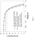
- FIG. 6 A comparison between a solar cell apparatus according to present invention and the relevant prior art is represented in Fig. 6 showing the I-V curves under AM1.5G illumination at 1 sun for two modules with a tandem solar cell configuration and a ZnO:B front TCO of about 1300nm with haze of 20% at 550nm.
- the former module has no interface layer between a ZnO based TCO layer and a p-type a-Si, the latter has the p-type dopants graded multi-layers structure of the present invention.
- the use of the proposed p-type dopants graded multi-layers structure improves the I-V of the cell with ZnO:B front contact.
- the Voc is significantly increased, of more than 2% (corresponding to ⁇ 1.5V in our large area module).
- the fill factor is improved.
- the interface improvement has certainly raised the maximum power output of the module with ZnO:B front contact of more than 5W.
- the proposed nanocrystalline interfacial layer can significantly improve the Voc and the FF of the solar cell. Nevertheless, the insertion of the small gap nanocrystalline thin layer can slightly reduce the Jsc current due to some absorption in the doped thin layer. However the higher FF and Voc lead to a clear advantage with respect to the case of ZnO not provided with a p-type dopants graded multi-layers structure. Fig.
Landscapes
- Chemical & Material Sciences (AREA)
- General Chemical & Material Sciences (AREA)
- Chemical Kinetics & Catalysis (AREA)
- Engineering & Computer Science (AREA)
- Materials Engineering (AREA)
- Mechanical Engineering (AREA)
- Metallurgy (AREA)
- Organic Chemistry (AREA)
- Inorganic Chemistry (AREA)
- Photovoltaic Devices (AREA)
Claims (9)
- Solarzellenvorrichtung (100), umfassend:• ein Substrat (101);• eine transparente leitfähige Oxid- (TCO) Schicht (102) vom n-Typ aus Zinkoxid, die auf dem Substrat (101) abgeschieden ist;• eine p-i-n-Struktur (200), die auf der transparenten leitfähigen Oxid- (TCO) Schicht (102) vom n-Typ abgeschieden ist, umfassend∘ eine p-Typ-Schicht (103)∘ eine i-Typ-Schicht (104)∘ die n-Typ-Schicht (105)• eine Metall-Rückseitenschicht (106), die auf der n-Typ-Schicht (105) der p-i-n-Struktur (200) abgeschieden ist; wobei• die p-Typ-Schicht (103) eine mit p-Typ-Dotierstoffen abgestufte Mehrschichtstruktur (3) mit einem Dotierstoffkonzentrationsprofil umfasst, das als Funktion der Dicke der mit p-Typ-Dotierstoffen abgestuften Mehrschichtstruktur (3) variiert, wobei• die mit p-Typ-Dotierstoffen abgestufte Mehrschichtstruktur (3) Bor (B) als Dotierelement umfasst,• die mit p-Typ-Dotierstoffen abgestufte Mehrschichtstruktur (3) umfasst:∘ eine erste nanokristalline oder mikrokristalline p-Typ-Schicht (3a),∘ eine zweite amorphe p-Typ-Schicht (3b),∘ eine dritte amorphe p-Typ-Schicht (3c),∘ eine vierte amorphe p-Typ-Schicht (3d),∘ wobei die zweiten, dritten und vierten amorphen p-Typ-Schichten (3b, 3c, 3d) unterschiedliche Dotierstoffkonzentrationen aufweisen und die Bor-(B) Dotierstoffkonzentration vom höchsten Wert in der ersten nanokristallinen oder mikrokristallinen p-Typ-Schicht (3a) bis zum niedrigsten Wert in der vierten amorphen p-Typ-Schicht (3d) variiert, was ein sich verjüngendes Bor-Konzentrationsprofil kennzeichnet.
- Solarzellenvorrichtung (100) nach Anspruch 1, wobei die dritte amorphe p-Typ-Schicht (3c) eine kleinere durchschnittliche Kristallitgröße als die vierte amorphe p-Typ-Schicht (3d) aufweist, und die vierte amorphe p-Typ-Schicht (3d) eine kleinere durchschnittliche Kristallitgröße als die zweite amorphe p-Typ-Schicht (3b) aufweist.
- Solarzellenvorrichtung (100) nach einem der Ansprüche 1 bis 2, wobei die erste nanokristalline oder mikrokristalline p-Typ-Schicht (3a) Silizium (Si) oder Siliziumkarbid (SiC) umfasst.
- Solarzellenvorrichtung (100) nach einem der Ansprüche 1 bis 3, wobei die zweite amorphe p-Typ-Schicht (3b), die dritte amorphe p-Typ-Schicht (3c) und die vierte amorphe p-Typ-Schicht (3d) Silizium (Si) oder Siliziumkarbid (SiC) oder Silizium und Wasserstoff (Si-H) umfassen.
- Verfahren (400) zum Bilden einer Solarzellenvorrichtung (100), das folgende Schritte umfasst:• Abscheiden eines transparenten leitfähigen Oxids (TCO) (102) vom n-Typ aus Zinkoxid auf einem Substrat mittels plasmaunterstützter chemischer Gasphasenabscheidung (PECVD);• Bilden einer p-i-n-Struktur (200) umfassend:∘ Abscheiden einer p-Typ-Schicht (103) auf dem transparenten leitfähigen Oxid (TCO) (102) vom n-Typ mittels plasmaunterstützter chemischer Gasphasenabscheidung (PECVD);∘ Abscheiden einer i-Typ-Schicht (104) auf der p-Typ-Schicht (103) mittels plasmaunterstützter chemischer Gasphasenabscheidung (PECVD);∘ Abscheiden einer n-Typ-Schicht (105) auf der i-Typ-Schicht (104) mittels plasmaunterstützter chemischer Gasphasenabscheidung (PECVD);wobei das Abscheiden der in der p-i-n-Struktur (200) enthaltenen p-Typ Schicht (103) umfasst:• Bilden einer mit p-Typ-Dotierstoffen abgestuften Mehrschichtstruktur (3), die Bor als Dotierelement umfasst, mittels plasmaunterstützter chemischer Gasphasenabscheidung (PECVD), umfassend:∘ Abscheiden einer ersten nanokristallinen oder mikrokristallinen p-Typ-Schicht (003a) mit einer ersten Dotierstoffkonzentration auf dem transparenten leitfähigen Oxid (TCO) (102) vom n-Typ mittels plasmaunterstützter chemischer Gasphasenabscheidung (PECVD);∘ Abscheiden einer zweiten amorphen p-Typ-Schicht (3b) mit einer zweiten Dotierstoffkonzentration auf der ersten nanokristallinen oder mikrokristallinen p-Typ-Schicht (3a) mittels plasmaunterstützter chemischer Gasphasenabscheidung (PECVD);• Abscheiden einer dritten amorphen p-Typ-Schicht (3c) mit einer dritten Dotierstoffkonzentration auf der zweiten amorphen p-Typ-Schicht (3b) mittels plasmaunterstützter chemischer Gasphasenabscheidung (PECVD);• Abscheiden einer vierten amorphen p-Typ-Schicht (3d) mit einer vierten Dotierstoffkonzentration auf der dritten amorphen p-Typ-Schicht (3c) mittels plasmaunterstützter chemischer Gasphasenabscheidung (PECVD),• wobei die vierte Dotierstoffkonzentration kleiner als die dritte Dotierstoffkonzentration ist, die kleiner als die zweite Dotierstoffkonzentration ist, die kleiner als die erste Dotierstoffkonzentration ist.
- Verfahren nach Anspruch 5, wobei die dritte amorphe p-Typ-Schicht (3c) unter Erreichung einer kleineren durchschnittlichen Kristallitgröße als die vierte amorphe p-Typ-Schicht (3d) abgeschieden wird, und die vierte amorphe p-Typ-Schicht (3d) unter Erreichung einer kleineren durchschnittlichen Kristallitgröße als die zweite amorphe p-Typ-Schicht (3b) abgeschieden wird.
- Verfahren nach Anspruch 6, wobei die mit p-Typ-Dotierstoffen abgestufte Mehrschichtstruktur (3) mit einem variierenden SiH4/(SiH4 + H2) - Flussmittelverhältnis gebildet wird.
- Verfahren nach Anspruch 7, wobei die erste nanokristalline oder mikrokristalline p-Typ-Schicht (3a), die in der mit p-Typ-Dotierstoffen abgestuften Mehrschichtstruktur (3) enthalten ist, mit einem SiH4/(SiH4 + H2)-Flussgrößenverhältnis gebildet wird, das auf einen niedrigeren Wert als den eingestellt ist, der zur Herstellung der zweiten amorphen p-Typ-Schicht (3b) verwendet wird, die zweite amorphe p-Typ-Schicht (3b) mit einem SiH4/(SiH4 + H2)-Flussgrößenverhältnis gebildet wird, das auf einen niedrigeren Wert als den eingestellt ist, der zur Herstellung der dritten amorphen p-Typ-Schicht (3c) verwendet wird, und die dritte amorphe p-Typ-Schicht (3c) mit einem SiH4/(SiH4 + H2)-Flussmittelverhältnis gebildet wird, das auf einen höheren Wert als den eingestellt ist, der zur Herstellung einer vierten amorphen p-Typ-Schicht (3d) verwendet wird.
- Verfahren nach einem der Ansprüche 5 bis 8, das ferner das Abscheiden einer Metall-Rückseitenschicht (106) auf der p-i-n-Struktur (200) umfasst.
Applications Claiming Priority (2)
| Application Number | Priority Date | Filing Date | Title |
|---|---|---|---|
| IT102016000096823A IT201600096823A1 (it) | 2016-09-27 | 2016-09-27 | Dispositivo a cella solare e metodo di produzione dello stesso |
| PCT/EP2017/074541 WO2018060278A1 (en) | 2016-09-27 | 2017-09-27 | Solar cell apparatus and method for forming the same |
Publications (2)
| Publication Number | Publication Date |
|---|---|
| EP3520146A1 EP3520146A1 (de) | 2019-08-07 |
| EP3520146B1 true EP3520146B1 (de) | 2022-01-19 |
Family
ID=58606529
Family Applications (1)
| Application Number | Title | Priority Date | Filing Date |
|---|---|---|---|
| EP17781039.7A Active EP3520146B1 (de) | 2016-09-27 | 2017-09-27 | Solarzellenvorrichtung und verfahren zur formung davon |
Country Status (3)
| Country | Link |
|---|---|
| EP (1) | EP3520146B1 (de) |
| IT (1) | IT201600096823A1 (de) |
| WO (1) | WO2018060278A1 (de) |
Families Citing this family (1)
| Publication number | Priority date | Publication date | Assignee | Title |
|---|---|---|---|---|
| CN114649425B (zh) * | 2022-05-20 | 2022-08-26 | 正泰新能科技有限公司 | 一种TopCon晶硅太阳能电池及其制备方法 |
Citations (1)
| Publication number | Priority date | Publication date | Assignee | Title |
|---|---|---|---|---|
| US20130048987A1 (en) * | 2011-08-26 | 2013-02-28 | Applied Materials, Inc. | P-i-n structures and methods for forming p-i-n structures having an i-layer formed via hot wire chemical vapor deposition (hwcvd) |
Family Cites Families (6)
| Publication number | Priority date | Publication date | Assignee | Title |
|---|---|---|---|---|
| JPS632385A (ja) * | 1986-06-23 | 1988-01-07 | Hitachi Ltd | 多層構造p型シリコン膜および太陽電池 |
| DE102005013537A1 (de) * | 2004-03-24 | 2005-10-20 | Sharp Kk | Fotoelektrischer Wandler und Herstellverfahren für einen solchen |
| US8652871B2 (en) * | 2008-08-29 | 2014-02-18 | Tel Solar Ag | Method for depositing an amorphous silicon film for photovoltaic devices with reduced light-induced degradation for improved stabilized performance |
| JP2010283161A (ja) * | 2009-06-04 | 2010-12-16 | Sanyo Electric Co Ltd | 太陽電池及びその製造方法 |
| CN102782881A (zh) * | 2009-09-18 | 2012-11-14 | 欧瑞康太阳能股份公司(特吕巴赫) | 高效率非晶硅光伏器件 |
| US20120211069A1 (en) * | 2011-02-23 | 2012-08-23 | Electronics And Telecommunications Research Institute | Thin-film solar cells and methods of fabricating the same |
-
2016
- 2016-09-27 IT IT102016000096823A patent/IT201600096823A1/it unknown
-
2017
- 2017-09-27 EP EP17781039.7A patent/EP3520146B1/de active Active
- 2017-09-27 WO PCT/EP2017/074541 patent/WO2018060278A1/en not_active Ceased
Patent Citations (1)
| Publication number | Priority date | Publication date | Assignee | Title |
|---|---|---|---|---|
| US20130048987A1 (en) * | 2011-08-26 | 2013-02-28 | Applied Materials, Inc. | P-i-n structures and methods for forming p-i-n structures having an i-layer formed via hot wire chemical vapor deposition (hwcvd) |
Also Published As
| Publication number | Publication date |
|---|---|
| IT201600096823A1 (it) | 2018-03-27 |
| EP3520146A1 (de) | 2019-08-07 |
| WO2018060278A1 (en) | 2018-04-05 |
Similar Documents
| Publication | Publication Date | Title |
|---|---|---|
| Mazzarella et al. | Nanocrystalline n-type silicon oxide front contacts for silicon heterojunction solar cells: photocurrent enhancement on planar and textured substrates | |
| US8030120B2 (en) | Hybrid window layer for photovoltaic cells | |
| AU729609B2 (en) | Photovoltaic device | |
| US8981200B2 (en) | Method for obtaining high performance thin film devices deposited on highly textured substrates | |
| US20110259395A1 (en) | Single Junction CIGS/CIS Solar Module | |
| US8679892B2 (en) | Method for manufacturing silicon thin-film solar cells | |
| US20100147361A1 (en) | Tandem junction photovoltaic device comprising copper indium gallium di-selenide bottom cell | |
| JPWO2001069690A1 (ja) | 光エネルギー変換装置 | |
| WO2010039727A1 (en) | Method and structure for thin film tandem photovoltaic cell | |
| US20150136210A1 (en) | Silicon-based solar cells with improved resistance to light-induced degradation | |
| US8785232B2 (en) | Photovoltaic device | |
| AU2011219223B2 (en) | Thin-film photoelectric conversion device and method for production thereof | |
| WO2013106439A1 (en) | High work-function buffer layers for silicon-based photovoltaic devices | |
| US20120318335A1 (en) | Tandem solar cell with improved tunnel junction | |
| US20110220198A1 (en) | Method and Device Utilizing Strained AZO Layer and Interfacial Fermi Level Pinning in Bifacial Thin Film PV Cells | |
| US20150136220A1 (en) | Method for production of a photovoltaic device in substrate configuration | |
| CN115516648A (zh) | 使用过渡金属氧化物的高效空穴传输层的方法 | |
| WO2018060278A1 (en) | Solar cell apparatus and method for forming the same | |
| EP3571723B1 (de) | Solarzellenvorrichtung und verfahren zur formung davon für einzel-, tandem- und heteroübergangssysteme | |
| Agbo et al. | Sensitivity of thin film nanocrystalline silicon properties to radio frequency plasma-enhanced chemical vapor deposition (rf PECVD) parameters | |
| JPH04255273A (ja) | 光起電力素子 | |
| CN102683482A (zh) | 用于形成双面薄膜光伏电池的方法和薄膜太阳能装置 |
Legal Events
| Date | Code | Title | Description |
|---|---|---|---|
| STAA | Information on the status of an ep patent application or granted ep patent |
Free format text: STATUS: UNKNOWN |
|
| STAA | Information on the status of an ep patent application or granted ep patent |
Free format text: STATUS: THE INTERNATIONAL PUBLICATION HAS BEEN MADE |
|
| PUAI | Public reference made under article 153(3) epc to a published international application that has entered the european phase |
Free format text: ORIGINAL CODE: 0009012 |
|
| STAA | Information on the status of an ep patent application or granted ep patent |
Free format text: STATUS: REQUEST FOR EXAMINATION WAS MADE |
|
| 17P | Request for examination filed |
Effective date: 20190408 |
|
| AK | Designated contracting states |
Kind code of ref document: A1 Designated state(s): AL AT BE BG CH CY CZ DE DK EE ES FI FR GB GR HR HU IE IS IT LI LT LU LV MC MK MT NL NO PL PT RO RS SE SI SK SM TR |
|
| AX | Request for extension of the european patent |
Extension state: BA ME |
|
| DAV | Request for validation of the european patent (deleted) | ||
| DAX | Request for extension of the european patent (deleted) | ||
| STAA | Information on the status of an ep patent application or granted ep patent |
Free format text: STATUS: EXAMINATION IS IN PROGRESS |
|
| 17Q | First examination report despatched |
Effective date: 20201008 |
|
| RAP1 | Party data changed (applicant data changed or rights of an application transferred) |
Owner name: ENEL GREEN POWER ITALIA S.R.L. |
|
| GRAP | Despatch of communication of intention to grant a patent |
Free format text: ORIGINAL CODE: EPIDOSNIGR1 |
|
| STAA | Information on the status of an ep patent application or granted ep patent |
Free format text: STATUS: GRANT OF PATENT IS INTENDED |
|
| RIC1 | Information provided on ipc code assigned before grant |
Ipc: C23C 16/40 20060101ALI20210831BHEP Ipc: C23C 16/32 20060101ALI20210831BHEP Ipc: C23C 16/02 20060101ALI20210831BHEP Ipc: C23C 16/24 20060101ALI20210831BHEP Ipc: C23C 16/44 20060101ALI20210831BHEP Ipc: H01L 21/02 20060101ALI20210831BHEP Ipc: H01L 31/075 20120101ALI20210831BHEP Ipc: H01L 31/20 20060101ALI20210831BHEP Ipc: H01L 31/065 20120101ALI20210831BHEP Ipc: H01L 31/0368 20060101AFI20210831BHEP |
|
| INTG | Intention to grant announced |
Effective date: 20211006 |
|
| GRAS | Grant fee paid |
Free format text: ORIGINAL CODE: EPIDOSNIGR3 |
|
| GRAA | (expected) grant |
Free format text: ORIGINAL CODE: 0009210 |
|
| STAA | Information on the status of an ep patent application or granted ep patent |
Free format text: STATUS: THE PATENT HAS BEEN GRANTED |
|
| AK | Designated contracting states |
Kind code of ref document: B1 Designated state(s): AL AT BE BG CH CY CZ DE DK EE ES FI FR GB GR HR HU IE IS IT LI LT LU LV MC MK MT NL NO PL PT RO RS SE SI SK SM TR |
|
| REG | Reference to a national code |
Ref country code: GB Ref legal event code: FG4D |
|
| REG | Reference to a national code |
Ref country code: CH Ref legal event code: EP |
|
| REG | Reference to a national code |
Ref country code: DE Ref legal event code: R096 Ref document number: 602017052528 Country of ref document: DE |
|
| REG | Reference to a national code |
Ref country code: AT Ref legal event code: REF Ref document number: 1464295 Country of ref document: AT Kind code of ref document: T Effective date: 20220215 |
|
| REG | Reference to a national code |
Ref country code: IE Ref legal event code: FG4D |
|
| REG | Reference to a national code |
Ref country code: LT Ref legal event code: MG9D |
|
| REG | Reference to a national code |
Ref country code: NL Ref legal event code: MP Effective date: 20220119 |
|
| REG | Reference to a national code |
Ref country code: AT Ref legal event code: MK05 Ref document number: 1464295 Country of ref document: AT Kind code of ref document: T Effective date: 20220119 |
|
| PG25 | Lapsed in a contracting state [announced via postgrant information from national office to epo] |
Ref country code: NL Free format text: LAPSE BECAUSE OF FAILURE TO SUBMIT A TRANSLATION OF THE DESCRIPTION OR TO PAY THE FEE WITHIN THE PRESCRIBED TIME-LIMIT Effective date: 20220119 |
|
| PG25 | Lapsed in a contracting state [announced via postgrant information from national office to epo] |
Ref country code: SE Free format text: LAPSE BECAUSE OF FAILURE TO SUBMIT A TRANSLATION OF THE DESCRIPTION OR TO PAY THE FEE WITHIN THE PRESCRIBED TIME-LIMIT Effective date: 20220119 Ref country code: RS Free format text: LAPSE BECAUSE OF FAILURE TO SUBMIT A TRANSLATION OF THE DESCRIPTION OR TO PAY THE FEE WITHIN THE PRESCRIBED TIME-LIMIT Effective date: 20220119 Ref country code: PT Free format text: LAPSE BECAUSE OF FAILURE TO SUBMIT A TRANSLATION OF THE DESCRIPTION OR TO PAY THE FEE WITHIN THE PRESCRIBED TIME-LIMIT Effective date: 20220519 Ref country code: NO Free format text: LAPSE BECAUSE OF FAILURE TO SUBMIT A TRANSLATION OF THE DESCRIPTION OR TO PAY THE FEE WITHIN THE PRESCRIBED TIME-LIMIT Effective date: 20220419 Ref country code: LT Free format text: LAPSE BECAUSE OF FAILURE TO SUBMIT A TRANSLATION OF THE DESCRIPTION OR TO PAY THE FEE WITHIN THE PRESCRIBED TIME-LIMIT Effective date: 20220119 Ref country code: HR Free format text: LAPSE BECAUSE OF FAILURE TO SUBMIT A TRANSLATION OF THE DESCRIPTION OR TO PAY THE FEE WITHIN THE PRESCRIBED TIME-LIMIT Effective date: 20220119 Ref country code: ES Free format text: LAPSE BECAUSE OF FAILURE TO SUBMIT A TRANSLATION OF THE DESCRIPTION OR TO PAY THE FEE WITHIN THE PRESCRIBED TIME-LIMIT Effective date: 20220119 Ref country code: BG Free format text: LAPSE BECAUSE OF FAILURE TO SUBMIT A TRANSLATION OF THE DESCRIPTION OR TO PAY THE FEE WITHIN THE PRESCRIBED TIME-LIMIT Effective date: 20220419 |
|
| PG25 | Lapsed in a contracting state [announced via postgrant information from national office to epo] |
Ref country code: PL Free format text: LAPSE BECAUSE OF FAILURE TO SUBMIT A TRANSLATION OF THE DESCRIPTION OR TO PAY THE FEE WITHIN THE PRESCRIBED TIME-LIMIT Effective date: 20220119 Ref country code: LV Free format text: LAPSE BECAUSE OF FAILURE TO SUBMIT A TRANSLATION OF THE DESCRIPTION OR TO PAY THE FEE WITHIN THE PRESCRIBED TIME-LIMIT Effective date: 20220119 Ref country code: GR Free format text: LAPSE BECAUSE OF FAILURE TO SUBMIT A TRANSLATION OF THE DESCRIPTION OR TO PAY THE FEE WITHIN THE PRESCRIBED TIME-LIMIT Effective date: 20220420 Ref country code: FI Free format text: LAPSE BECAUSE OF FAILURE TO SUBMIT A TRANSLATION OF THE DESCRIPTION OR TO PAY THE FEE WITHIN THE PRESCRIBED TIME-LIMIT Effective date: 20220119 Ref country code: AT Free format text: LAPSE BECAUSE OF FAILURE TO SUBMIT A TRANSLATION OF THE DESCRIPTION OR TO PAY THE FEE WITHIN THE PRESCRIBED TIME-LIMIT Effective date: 20220119 |
|
| PG25 | Lapsed in a contracting state [announced via postgrant information from national office to epo] |
Ref country code: IS Free format text: LAPSE BECAUSE OF FAILURE TO SUBMIT A TRANSLATION OF THE DESCRIPTION OR TO PAY THE FEE WITHIN THE PRESCRIBED TIME-LIMIT Effective date: 20220519 |
|
| REG | Reference to a national code |
Ref country code: DE Ref legal event code: R097 Ref document number: 602017052528 Country of ref document: DE |
|
| PG25 | Lapsed in a contracting state [announced via postgrant information from national office to epo] |
Ref country code: SM Free format text: LAPSE BECAUSE OF FAILURE TO SUBMIT A TRANSLATION OF THE DESCRIPTION OR TO PAY THE FEE WITHIN THE PRESCRIBED TIME-LIMIT Effective date: 20220119 Ref country code: SK Free format text: LAPSE BECAUSE OF FAILURE TO SUBMIT A TRANSLATION OF THE DESCRIPTION OR TO PAY THE FEE WITHIN THE PRESCRIBED TIME-LIMIT Effective date: 20220119 Ref country code: RO Free format text: LAPSE BECAUSE OF FAILURE TO SUBMIT A TRANSLATION OF THE DESCRIPTION OR TO PAY THE FEE WITHIN THE PRESCRIBED TIME-LIMIT Effective date: 20220119 Ref country code: EE Free format text: LAPSE BECAUSE OF FAILURE TO SUBMIT A TRANSLATION OF THE DESCRIPTION OR TO PAY THE FEE WITHIN THE PRESCRIBED TIME-LIMIT Effective date: 20220119 Ref country code: DK Free format text: LAPSE BECAUSE OF FAILURE TO SUBMIT A TRANSLATION OF THE DESCRIPTION OR TO PAY THE FEE WITHIN THE PRESCRIBED TIME-LIMIT Effective date: 20220119 Ref country code: CZ Free format text: LAPSE BECAUSE OF FAILURE TO SUBMIT A TRANSLATION OF THE DESCRIPTION OR TO PAY THE FEE WITHIN THE PRESCRIBED TIME-LIMIT Effective date: 20220119 |
|
| PLBE | No opposition filed within time limit |
Free format text: ORIGINAL CODE: 0009261 |
|
| STAA | Information on the status of an ep patent application or granted ep patent |
Free format text: STATUS: NO OPPOSITION FILED WITHIN TIME LIMIT |
|
| PG25 | Lapsed in a contracting state [announced via postgrant information from national office to epo] |
Ref country code: AL Free format text: LAPSE BECAUSE OF FAILURE TO SUBMIT A TRANSLATION OF THE DESCRIPTION OR TO PAY THE FEE WITHIN THE PRESCRIBED TIME-LIMIT Effective date: 20220119 |
|
| 26N | No opposition filed |
Effective date: 20221020 |
|
| PG25 | Lapsed in a contracting state [announced via postgrant information from national office to epo] |
Ref country code: SI Free format text: LAPSE BECAUSE OF FAILURE TO SUBMIT A TRANSLATION OF THE DESCRIPTION OR TO PAY THE FEE WITHIN THE PRESCRIBED TIME-LIMIT Effective date: 20220119 |
|
| REG | Reference to a national code |
Ref country code: GB Ref legal event code: 732E Free format text: REGISTERED BETWEEN 20230309 AND 20230315 |
|
| PG25 | Lapsed in a contracting state [announced via postgrant information from national office to epo] |
Ref country code: MC Free format text: LAPSE BECAUSE OF FAILURE TO SUBMIT A TRANSLATION OF THE DESCRIPTION OR TO PAY THE FEE WITHIN THE PRESCRIBED TIME-LIMIT Effective date: 20220119 |
|
| REG | Reference to a national code |
Ref country code: CH Ref legal event code: PL |
|
| REG | Reference to a national code |
Ref country code: DE Ref legal event code: R081 Ref document number: 602017052528 Country of ref document: DE Owner name: 3SUN S.R.L., IT Free format text: FORMER OWNER: ENEL GREEN POWER ITALIA S.R.L., ROME, IT |
|
| REG | Reference to a national code |
Ref country code: BE Ref legal event code: MM Effective date: 20220930 |
|
| PG25 | Lapsed in a contracting state [announced via postgrant information from national office to epo] |
Ref country code: LU Free format text: LAPSE BECAUSE OF NON-PAYMENT OF DUE FEES Effective date: 20220927 |
|
| P01 | Opt-out of the competence of the unified patent court (upc) registered |
Effective date: 20230607 |
|
| PG25 | Lapsed in a contracting state [announced via postgrant information from national office to epo] |
Ref country code: LI Free format text: LAPSE BECAUSE OF NON-PAYMENT OF DUE FEES Effective date: 20220930 Ref country code: IE Free format text: LAPSE BECAUSE OF NON-PAYMENT OF DUE FEES Effective date: 20220927 Ref country code: CH Free format text: LAPSE BECAUSE OF NON-PAYMENT OF DUE FEES Effective date: 20220930 |
|
| PG25 | Lapsed in a contracting state [announced via postgrant information from national office to epo] |
Ref country code: BE Free format text: LAPSE BECAUSE OF NON-PAYMENT OF DUE FEES Effective date: 20220930 |
|
| PG25 | Lapsed in a contracting state [announced via postgrant information from national office to epo] |
Ref country code: HU Free format text: LAPSE BECAUSE OF FAILURE TO SUBMIT A TRANSLATION OF THE DESCRIPTION OR TO PAY THE FEE WITHIN THE PRESCRIBED TIME-LIMIT; INVALID AB INITIO Effective date: 20170927 |
|
| PG25 | Lapsed in a contracting state [announced via postgrant information from national office to epo] |
Ref country code: CY Free format text: LAPSE BECAUSE OF FAILURE TO SUBMIT A TRANSLATION OF THE DESCRIPTION OR TO PAY THE FEE WITHIN THE PRESCRIBED TIME-LIMIT Effective date: 20220119 |
|
| PG25 | Lapsed in a contracting state [announced via postgrant information from national office to epo] |
Ref country code: MK Free format text: LAPSE BECAUSE OF FAILURE TO SUBMIT A TRANSLATION OF THE DESCRIPTION OR TO PAY THE FEE WITHIN THE PRESCRIBED TIME-LIMIT Effective date: 20220119 |
|
| PG25 | Lapsed in a contracting state [announced via postgrant information from national office to epo] |
Ref country code: TR Free format text: LAPSE BECAUSE OF FAILURE TO SUBMIT A TRANSLATION OF THE DESCRIPTION OR TO PAY THE FEE WITHIN THE PRESCRIBED TIME-LIMIT Effective date: 20220119 |
|
| PG25 | Lapsed in a contracting state [announced via postgrant information from national office to epo] |
Ref country code: MT Free format text: LAPSE BECAUSE OF FAILURE TO SUBMIT A TRANSLATION OF THE DESCRIPTION OR TO PAY THE FEE WITHIN THE PRESCRIBED TIME-LIMIT Effective date: 20220119 |
|
| REG | Reference to a national code |
Ref country code: DE Ref legal event code: R079 Ref document number: 602017052528 Country of ref document: DE Free format text: PREVIOUS MAIN CLASS: H01L0031036800 Ipc: H10F0077164000 |
|
| PGFP | Annual fee paid to national office [announced via postgrant information from national office to epo] |
Ref country code: DE Payment date: 20250919 Year of fee payment: 9 |
|
| PGFP | Annual fee paid to national office [announced via postgrant information from national office to epo] |
Ref country code: IT Payment date: 20250724 Year of fee payment: 9 |
|
| PGFP | Annual fee paid to national office [announced via postgrant information from national office to epo] |
Ref country code: GB Payment date: 20250919 Year of fee payment: 9 |
|
| PGFP | Annual fee paid to national office [announced via postgrant information from national office to epo] |
Ref country code: FR Payment date: 20250922 Year of fee payment: 9 |