EP3515872B1 - Substrat revetu d'un revetement bas-emissif - Google Patents
Substrat revetu d'un revetement bas-emissif Download PDFInfo
- Publication number
- EP3515872B1 EP3515872B1 EP17780504.1A EP17780504A EP3515872B1 EP 3515872 B1 EP3515872 B1 EP 3515872B1 EP 17780504 A EP17780504 A EP 17780504A EP 3515872 B1 EP3515872 B1 EP 3515872B1
- Authority
- EP
- European Patent Office
- Prior art keywords
- layer
- oxide
- dielectric layer
- substrate
- oxygen
- Prior art date
- Legal status (The legal status is an assumption and is not a legal conclusion. Google has not performed a legal analysis and makes no representation as to the accuracy of the status listed.)
- Active
Links
- 239000000758 substrate Substances 0.000 title claims description 93
- 238000000576 coating method Methods 0.000 title description 9
- 239000011248 coating agent Substances 0.000 title description 7
- XLOMVQKBTHCTTD-UHFFFAOYSA-N Zinc monoxide Chemical compound [Zn]=O XLOMVQKBTHCTTD-UHFFFAOYSA-N 0.000 claims description 158
- 239000011787 zinc oxide Substances 0.000 claims description 79
- 239000010936 titanium Substances 0.000 claims description 54
- BQCADISMDOOEFD-UHFFFAOYSA-N Silver Chemical compound [Ag] BQCADISMDOOEFD-UHFFFAOYSA-N 0.000 claims description 44
- 229910052709 silver Inorganic materials 0.000 claims description 44
- 239000004332 silver Substances 0.000 claims description 44
- OGIDPMRJRNCKJF-UHFFFAOYSA-N titanium oxide Inorganic materials [Ti]=O OGIDPMRJRNCKJF-UHFFFAOYSA-N 0.000 claims description 43
- 238000000034 method Methods 0.000 claims description 37
- 230000008569 process Effects 0.000 claims description 28
- 238000009736 wetting Methods 0.000 claims description 28
- GWEVSGVZZGPLCZ-UHFFFAOYSA-N Titan oxide Chemical compound O=[Ti]=O GWEVSGVZZGPLCZ-UHFFFAOYSA-N 0.000 claims description 26
- 239000011521 glass Substances 0.000 claims description 26
- 229910003087 TiOx Inorganic materials 0.000 claims description 25
- HLLICFJUWSZHRJ-UHFFFAOYSA-N tioxidazole Chemical compound CCCOC1=CC=C2N=C(NC(=O)OC)SC2=C1 HLLICFJUWSZHRJ-UHFFFAOYSA-N 0.000 claims description 25
- 230000005855 radiation Effects 0.000 claims description 19
- 239000000463 material Substances 0.000 claims description 15
- 238000011282 treatment Methods 0.000 claims description 10
- ATJFFYVFTNAWJD-UHFFFAOYSA-N Tin Chemical compound [Sn] ATJFFYVFTNAWJD-UHFFFAOYSA-N 0.000 claims description 9
- RTAQQCXQSZGOHL-UHFFFAOYSA-N Titanium Chemical compound [Ti] RTAQQCXQSZGOHL-UHFFFAOYSA-N 0.000 claims description 6
- 239000002241 glass-ceramic Substances 0.000 claims description 5
- 239000010955 niobium Substances 0.000 claims description 3
- GUCVJGMIXFAOAE-UHFFFAOYSA-N niobium atom Chemical compound [Nb] GUCVJGMIXFAOAE-UHFFFAOYSA-N 0.000 claims description 3
- 229910052814 silicon oxide Inorganic materials 0.000 claims description 3
- 239000011701 zinc Substances 0.000 claims description 3
- XUIMIQQOPSSXEZ-UHFFFAOYSA-N Silicon Chemical compound [Si] XUIMIQQOPSSXEZ-UHFFFAOYSA-N 0.000 claims description 2
- HCHKCACWOHOZIP-UHFFFAOYSA-N Zinc Chemical compound [Zn] HCHKCACWOHOZIP-UHFFFAOYSA-N 0.000 claims description 2
- CPLXHLVBOLITMK-UHFFFAOYSA-N magnesium oxide Inorganic materials [Mg]=O CPLXHLVBOLITMK-UHFFFAOYSA-N 0.000 claims description 2
- 239000000395 magnesium oxide Substances 0.000 claims description 2
- AXZKOIWUVFPNLO-UHFFFAOYSA-N magnesium;oxygen(2-) Chemical compound [O-2].[Mg+2] AXZKOIWUVFPNLO-UHFFFAOYSA-N 0.000 claims description 2
- 229910000484 niobium oxide Inorganic materials 0.000 claims description 2
- 239000010703 silicon Substances 0.000 claims description 2
- 229910052725 zinc Inorganic materials 0.000 claims description 2
- 229920000620 organic polymer Polymers 0.000 claims 2
- 239000002861 polymer material Substances 0.000 claims 2
- 230000003247 decreasing effect Effects 0.000 claims 1
- 239000010410 layer Substances 0.000 description 265
- QVGXLLKOCUKJST-UHFFFAOYSA-N atomic oxygen Chemical compound [O] QVGXLLKOCUKJST-UHFFFAOYSA-N 0.000 description 22
- 229910052760 oxygen Inorganic materials 0.000 description 22
- 239000001301 oxygen Substances 0.000 description 22
- 229910052581 Si3N4 Inorganic materials 0.000 description 19
- 238000000151 deposition Methods 0.000 description 19
- 230000008021 deposition Effects 0.000 description 18
- 238000010438 heat treatment Methods 0.000 description 18
- 229910010413 TiO 2 Inorganic materials 0.000 description 15
- 238000010521 absorption reaction Methods 0.000 description 9
- 238000002425 crystallisation Methods 0.000 description 8
- 230000008025 crystallization Effects 0.000 description 8
- 238000009434 installation Methods 0.000 description 8
- 239000011241 protective layer Substances 0.000 description 8
- 239000000835 fiber Substances 0.000 description 7
- 229910052751 metal Inorganic materials 0.000 description 7
- 239000002184 metal Substances 0.000 description 7
- 230000005540 biological transmission Effects 0.000 description 6
- 238000005224 laser annealing Methods 0.000 description 6
- 230000003287 optical effect Effects 0.000 description 6
- 238000012545 processing Methods 0.000 description 6
- 238000004519 manufacturing process Methods 0.000 description 5
- 150000004767 nitrides Chemical class 0.000 description 5
- 239000011368 organic material Substances 0.000 description 5
- 238000004544 sputter deposition Methods 0.000 description 5
- 229910001887 tin oxide Inorganic materials 0.000 description 5
- PXHVJJICTQNCMI-UHFFFAOYSA-N Nickel Chemical compound [Ni] PXHVJJICTQNCMI-UHFFFAOYSA-N 0.000 description 4
- 230000008901 benefit Effects 0.000 description 4
- 230000014509 gene expression Effects 0.000 description 4
- 230000033001 locomotion Effects 0.000 description 4
- 229910052719 titanium Inorganic materials 0.000 description 4
- 229910052782 aluminium Inorganic materials 0.000 description 3
- XAGFODPZIPBFFR-UHFFFAOYSA-N aluminium Chemical compound [Al] XAGFODPZIPBFFR-UHFFFAOYSA-N 0.000 description 3
- 230000000694 effects Effects 0.000 description 3
- 239000007789 gas Substances 0.000 description 3
- 239000013307 optical fiber Substances 0.000 description 3
- HQVNEWCFYHHQES-UHFFFAOYSA-N silicon nitride Chemical compound N12[Si]34N5[Si]62N3[Si]51N64 HQVNEWCFYHHQES-UHFFFAOYSA-N 0.000 description 3
- XOLBLPGZBRYERU-UHFFFAOYSA-N tin dioxide Chemical compound O=[Sn]=O XOLBLPGZBRYERU-UHFFFAOYSA-N 0.000 description 3
- 238000013519 translation Methods 0.000 description 3
- VYZAMTAEIAYCRO-UHFFFAOYSA-N Chromium Chemical compound [Cr] VYZAMTAEIAYCRO-UHFFFAOYSA-N 0.000 description 2
- 229910045601 alloy Inorganic materials 0.000 description 2
- 239000000956 alloy Substances 0.000 description 2
- 239000011651 chromium Substances 0.000 description 2
- 229910052804 chromium Inorganic materials 0.000 description 2
- 230000001427 coherent effect Effects 0.000 description 2
- 230000007547 defect Effects 0.000 description 2
- 230000031700 light absorption Effects 0.000 description 2
- 229910044991 metal oxide Inorganic materials 0.000 description 2
- 150000004706 metal oxides Chemical class 0.000 description 2
- 150000002739 metals Chemical class 0.000 description 2
- 230000005012 migration Effects 0.000 description 2
- 238000013508 migration Methods 0.000 description 2
- 239000000203 mixture Substances 0.000 description 2
- 229910052759 nickel Inorganic materials 0.000 description 2
- 229910000623 nickel–chromium alloy Inorganic materials 0.000 description 2
- 230000003647 oxidation Effects 0.000 description 2
- 238000007254 oxidation reaction Methods 0.000 description 2
- 229920000139 polyethylene terephthalate Polymers 0.000 description 2
- 239000005020 polyethylene terephthalate Substances 0.000 description 2
- 238000011084 recovery Methods 0.000 description 2
- 239000000126 substance Substances 0.000 description 2
- 229910018072 Al 2 O 3 Inorganic materials 0.000 description 1
- 229910000906 Bronze Inorganic materials 0.000 description 1
- 229910000990 Ni alloy Inorganic materials 0.000 description 1
- VYPSYNLAJGMNEJ-UHFFFAOYSA-N Silicium dioxide Chemical compound O=[Si]=O VYPSYNLAJGMNEJ-UHFFFAOYSA-N 0.000 description 1
- 229910006404 SnO 2 Inorganic materials 0.000 description 1
- 229910005728 SnZn Inorganic materials 0.000 description 1
- 238000002441 X-ray diffraction Methods 0.000 description 1
- HZEWFHLRYVTOIW-UHFFFAOYSA-N [Ti].[Ni] Chemical compound [Ti].[Ni] HZEWFHLRYVTOIW-UHFFFAOYSA-N 0.000 description 1
- 230000002745 absorbent Effects 0.000 description 1
- 239000002250 absorbent Substances 0.000 description 1
- 239000005407 aluminoborosilicate glass Substances 0.000 description 1
- 230000003321 amplification Effects 0.000 description 1
- 230000008033 biological extinction Effects 0.000 description 1
- 239000005388 borosilicate glass Substances 0.000 description 1
- 239000010974 bronze Substances 0.000 description 1
- 239000002800 charge carrier Substances 0.000 description 1
- 229910052729 chemical element Inorganic materials 0.000 description 1
- 238000006243 chemical reaction Methods 0.000 description 1
- 239000000788 chromium alloy Substances 0.000 description 1
- 238000004140 cleaning Methods 0.000 description 1
- 238000010924 continuous production Methods 0.000 description 1
- 238000001816 cooling Methods 0.000 description 1
- KUNSUQLRTQLHQQ-UHFFFAOYSA-N copper tin Chemical compound [Cu].[Sn] KUNSUQLRTQLHQQ-UHFFFAOYSA-N 0.000 description 1
- 239000013078 crystal Substances 0.000 description 1
- 238000005520 cutting process Methods 0.000 description 1
- 238000005137 deposition process Methods 0.000 description 1
- 230000002542 deteriorative effect Effects 0.000 description 1
- 230000008034 disappearance Effects 0.000 description 1
- 238000006073 displacement reaction Methods 0.000 description 1
- 230000002349 favourable effect Effects 0.000 description 1
- 230000006698 induction Effects 0.000 description 1
- 150000002484 inorganic compounds Chemical class 0.000 description 1
- 229910010272 inorganic material Inorganic materials 0.000 description 1
- 238000005259 measurement Methods 0.000 description 1
- 230000007246 mechanism Effects 0.000 description 1
- 239000006060 molten glass Substances 0.000 description 1
- 229910001000 nickel titanium Inorganic materials 0.000 description 1
- 229910052758 niobium Inorganic materials 0.000 description 1
- 230000006911 nucleation Effects 0.000 description 1
- 238000010899 nucleation Methods 0.000 description 1
- 238000003199 nucleic acid amplification method Methods 0.000 description 1
- 230000001590 oxidative effect Effects 0.000 description 1
- 239000012071 phase Substances 0.000 description 1
- 229920003229 poly(methyl methacrylate) Polymers 0.000 description 1
- 239000004417 polycarbonate Substances 0.000 description 1
- 229920000515 polycarbonate Polymers 0.000 description 1
- -1 polyethylene terephthalate Polymers 0.000 description 1
- 239000004926 polymethyl methacrylate Substances 0.000 description 1
- 230000001737 promoting effect Effects 0.000 description 1
- 238000005086 pumping Methods 0.000 description 1
- 230000009467 reduction Effects 0.000 description 1
- 238000005096 rolling process Methods 0.000 description 1
- 150000003378 silver Chemical class 0.000 description 1
- 239000005361 soda-lime glass Substances 0.000 description 1
- 239000007790 solid phase Substances 0.000 description 1
- 230000009466 transformation Effects 0.000 description 1
- 238000001771 vacuum deposition Methods 0.000 description 1
Images
Classifications
-
- C—CHEMISTRY; METALLURGY
- C03—GLASS; MINERAL OR SLAG WOOL
- C03C—CHEMICAL COMPOSITION OF GLASSES, GLAZES OR VITREOUS ENAMELS; SURFACE TREATMENT OF GLASS; SURFACE TREATMENT OF FIBRES OR FILAMENTS MADE FROM GLASS, MINERALS OR SLAGS; JOINING GLASS TO GLASS OR OTHER MATERIALS
- C03C17/00—Surface treatment of glass, not in the form of fibres or filaments, by coating
- C03C17/34—Surface treatment of glass, not in the form of fibres or filaments, by coating with at least two coatings having different compositions
- C03C17/36—Surface treatment of glass, not in the form of fibres or filaments, by coating with at least two coatings having different compositions at least one coating being a metal
- C03C17/3602—Surface treatment of glass, not in the form of fibres or filaments, by coating with at least two coatings having different compositions at least one coating being a metal the metal being present as a layer
- C03C17/3626—Surface treatment of glass, not in the form of fibres or filaments, by coating with at least two coatings having different compositions at least one coating being a metal the metal being present as a layer one layer at least containing a nitride, oxynitride, boronitride or carbonitride
-
- C—CHEMISTRY; METALLURGY
- C03—GLASS; MINERAL OR SLAG WOOL
- C03C—CHEMICAL COMPOSITION OF GLASSES, GLAZES OR VITREOUS ENAMELS; SURFACE TREATMENT OF GLASS; SURFACE TREATMENT OF FIBRES OR FILAMENTS MADE FROM GLASS, MINERALS OR SLAGS; JOINING GLASS TO GLASS OR OTHER MATERIALS
- C03C17/00—Surface treatment of glass, not in the form of fibres or filaments, by coating
- C03C17/34—Surface treatment of glass, not in the form of fibres or filaments, by coating with at least two coatings having different compositions
- C03C17/36—Surface treatment of glass, not in the form of fibres or filaments, by coating with at least two coatings having different compositions at least one coating being a metal
- C03C17/3602—Surface treatment of glass, not in the form of fibres or filaments, by coating with at least two coatings having different compositions at least one coating being a metal the metal being present as a layer
- C03C17/3644—Surface treatment of glass, not in the form of fibres or filaments, by coating with at least two coatings having different compositions at least one coating being a metal the metal being present as a layer the metal being silver
-
- C—CHEMISTRY; METALLURGY
- C03—GLASS; MINERAL OR SLAG WOOL
- C03C—CHEMICAL COMPOSITION OF GLASSES, GLAZES OR VITREOUS ENAMELS; SURFACE TREATMENT OF GLASS; SURFACE TREATMENT OF FIBRES OR FILAMENTS MADE FROM GLASS, MINERALS OR SLAGS; JOINING GLASS TO GLASS OR OTHER MATERIALS
- C03C17/00—Surface treatment of glass, not in the form of fibres or filaments, by coating
- C03C17/34—Surface treatment of glass, not in the form of fibres or filaments, by coating with at least two coatings having different compositions
- C03C17/36—Surface treatment of glass, not in the form of fibres or filaments, by coating with at least two coatings having different compositions at least one coating being a metal
- C03C17/3602—Surface treatment of glass, not in the form of fibres or filaments, by coating with at least two coatings having different compositions at least one coating being a metal the metal being present as a layer
- C03C17/3652—Surface treatment of glass, not in the form of fibres or filaments, by coating with at least two coatings having different compositions at least one coating being a metal the metal being present as a layer the coating stack containing at least one sacrificial layer to protect the metal from oxidation
-
- C—CHEMISTRY; METALLURGY
- C03—GLASS; MINERAL OR SLAG WOOL
- C03C—CHEMICAL COMPOSITION OF GLASSES, GLAZES OR VITREOUS ENAMELS; SURFACE TREATMENT OF GLASS; SURFACE TREATMENT OF FIBRES OR FILAMENTS MADE FROM GLASS, MINERALS OR SLAGS; JOINING GLASS TO GLASS OR OTHER MATERIALS
- C03C17/00—Surface treatment of glass, not in the form of fibres or filaments, by coating
- C03C17/34—Surface treatment of glass, not in the form of fibres or filaments, by coating with at least two coatings having different compositions
- C03C17/36—Surface treatment of glass, not in the form of fibres or filaments, by coating with at least two coatings having different compositions at least one coating being a metal
- C03C17/3602—Surface treatment of glass, not in the form of fibres or filaments, by coating with at least two coatings having different compositions at least one coating being a metal the metal being present as a layer
- C03C17/3657—Surface treatment of glass, not in the form of fibres or filaments, by coating with at least two coatings having different compositions at least one coating being a metal the metal being present as a layer the multilayer coating having optical properties
- C03C17/366—Low-emissivity or solar control coatings
-
- C—CHEMISTRY; METALLURGY
- C03—GLASS; MINERAL OR SLAG WOOL
- C03C—CHEMICAL COMPOSITION OF GLASSES, GLAZES OR VITREOUS ENAMELS; SURFACE TREATMENT OF GLASS; SURFACE TREATMENT OF FIBRES OR FILAMENTS MADE FROM GLASS, MINERALS OR SLAGS; JOINING GLASS TO GLASS OR OTHER MATERIALS
- C03C17/00—Surface treatment of glass, not in the form of fibres or filaments, by coating
- C03C17/34—Surface treatment of glass, not in the form of fibres or filaments, by coating with at least two coatings having different compositions
- C03C17/36—Surface treatment of glass, not in the form of fibres or filaments, by coating with at least two coatings having different compositions at least one coating being a metal
- C03C17/3602—Surface treatment of glass, not in the form of fibres or filaments, by coating with at least two coatings having different compositions at least one coating being a metal the metal being present as a layer
- C03C17/3681—Surface treatment of glass, not in the form of fibres or filaments, by coating with at least two coatings having different compositions at least one coating being a metal the metal being present as a layer the multilayer coating being used in glazing, e.g. windows or windscreens
-
- C—CHEMISTRY; METALLURGY
- C03—GLASS; MINERAL OR SLAG WOOL
- C03C—CHEMICAL COMPOSITION OF GLASSES, GLAZES OR VITREOUS ENAMELS; SURFACE TREATMENT OF GLASS; SURFACE TREATMENT OF FIBRES OR FILAMENTS MADE FROM GLASS, MINERALS OR SLAGS; JOINING GLASS TO GLASS OR OTHER MATERIALS
- C03C2218/00—Methods for coating glass
- C03C2218/30—Aspects of methods for coating glass not covered above
- C03C2218/32—After-treatment
Definitions
- the invention relates to the field of inorganic thin layers, in particular deposited on glass substrates. It relates more particularly to a process for obtaining a material comprising a substrate coated on at least one face with a stack of low-emissivity thin layers.
- optical properties for example of reflection or absorption of radiation of a range of wavelengths data, particular electrical conduction properties, or even properties related to the ease of cleaning or the possibility for the material to self-clean.
- a plasma is created under a high vacuum in the vicinity of a target comprising the chemical elements to be deposited.
- the active species of the plasma by bombarding the target, tear off said elements, which are deposited on the substrate, forming the desired thin layer.
- This process is said to be “reactive” when the layer consists of a material resulting from a chemical reaction between the elements torn from the target and the gas contained in the plasma.
- the major advantage of this method lies in the possibility of depositing on the same line a very complex stack of layers by successively making the substrate pass under different targets, this generally in a single and same device.
- thin layers are most often based on inorganic compounds: oxides, nitrides, or even metals. Their thickness generally varies from a few nanometers to a few hundred nanometers, hence their qualifier “thin”.
- the thin layers based on metallic silver which have properties of electrical conduction and reflection of infrared radiation, hence their use in solar control glazing, in particular solar protection (aimed at reducing the incoming solar energy) and/or low emissivity (aimed at reducing the amount of energy dissipated outside a building or vehicle).
- the or each layer of silver is generally inserted in a stack of layers.
- the or each silver-based thin layer is generally arranged between two dielectric thin layers based on oxide or nitride (for example TiO 2 , SnO 2 or Si 3N4 ) .
- These layers are respectively called wetting layer and blocker layer.
- WO 2010/142926 describes stacks of low-emission thin layers comprising in particular a silver layer, dielectric layers based on TiO 2 and Si 2 N 3 , a wetting layer based on ZnO and a layer of titanium blocker.
- the silver layers have the particularity of seeing some of their properties improved when they are in an at least partially crystallized state. It is generally sought to increase as much as possible the rate of crystallization of these layers (the mass or volume proportion of crystallized material) and the size of the crystalline grains (or the size of coherent diffraction domains measured by X-ray diffraction methods). It is known in particular that silver layers having a high crystallization rate and consequently a low residual content of nanometric grains have lower emissivity and resistivity as well as higher transmission in the visible than silver layers. mostly nano-crystallized. The electrical conductivity and the low emissivity properties of these layers are thus improved. The increase in the size of the grains is in fact accompanied by a reduction in the grain boundaries, favorable to the mobility of the electric charge carriers.
- the silver layers deposited by the magnetron process are generally mostly or even completely nano-crystallized (the average size of the crystalline grains being less than a few nanometers), and heat treatments prove necessary to obtain the desired crystallization rate or the grain size. desired.
- the thin oxide-based dielectric layers are generally deposited by a reactive magnetron process from a metallic or substoichiometric oxide target in a plasma containing oxygen.
- the process parameters are then generally adjusted so as to obtain the desired oxide in a stoichiometric proportion.
- the deposited oxide layer may have a sub-stoichiometric composition. It was observed that, in this case, the resistivity gain of the silver layers after laser annealing was not as good as expected. Indeed, below a certain scrolling speed threshold, the gain in resistivity may tend to decrease with the decrease in the scrolling speed whereas the latter should on the contrary increase.
- the expression "in the vicinity of” associated with the position of a first layer (in particular the oxygen donor layer) with respect to a second layer (in particular the dielectric layer based on oxide) means the first layer maybe above or below the second layer, these which may be in contact with or separated from each other by other layers, in particular up to two other layers, preferably at most one other layer.
- the terms “below” and “above”, associated with the position of a first layer with respect to a second layer mean that the first layer is closer, respectively further away, from the substrate than the second layer. These terms do not however exclude the presence of other layers between said first and second layers.
- a first layer "in direct contact” with a second layer means that no other layer is placed between them. The same goes for the expressions “directly above” and “directly below”. Thus, it is understood that, unless indicated otherwise, other layers can be interposed between each of the layers of the stack.
- the oxide-based dielectric layer is under-stoichiometric in oxygen, it tends to reduce the surrounding layers by "pumping" oxygen from the surrounding layers. , in particular of the wetting layer, under the effect of laser annealing. This would have the effect of altering the wetting layer on which the silver layer crystallizes and consequently deteriorating the quality of the silver layer.
- the presence of an oxygen-donating layer in the vicinity of the oxide-based dielectric layer makes it possible to prevent this phenomenon.
- the oxygen pumped by the oxide-based dielectric layer will indeed come primarily from the oxygen-donating layer, which has the effect of protecting and protecting the wetting layer.
- the substrate is a sheet of glass, glass-ceramic, or a polymeric organic material. It is preferably transparent, colorless (it is then a clear or extra-clear glass) or colored, for example blue, green, gray or bronze.
- the glass is preferably of the silico-soda-lime type, but it can also be of borosilicate or alumino-borosilicate glass.
- the preferred polymeric organic materials are polycarbonate or polymethyl methacrylate or else polyethylene terephthalate (PET).
- PET polyethylene terephthalate
- the substrate advantageously has at least one dimension greater than or equal to 1 m, or even 2 m and even 3 m.
- the thickness of the substrate generally varies between 0.5 mm and 19 mm, preferably between 0.7 and 9 mm, in particular between 2 and 8 mm, or even between 4 and 6 mm.
- the substrate can be flat or curved, even flexible.
- the glass substrate is preferably of the float type, that is to say likely to have been obtained by a process consisting in pouring the molten glass onto a bath of molten tin (“float” bath).
- the layer to be treated can just as easily be deposited on the “tin” face as on the “atmosphere” face of the substrate.
- atmosphere and tin faces is meant the faces of the substrate having been respectively in contact with the atmosphere prevailing in the float bath and in contact with the molten tin.
- the tin face contains a small surface quantity of tin having diffused into the structure of the glass.
- the glass substrate can also be obtained by rolling between two rollers, a technique which makes it possible in particular to print patterns on the surface of the glass.
- clear glass is meant a silico-soda-lime glass obtained by floating, not coated with layers, and having a light transmission of the order of 90%, a light reflection of the order of 8% and an energy transmission of l order of 83% for a thickness of 4 mm.
- Light and energy transmissions and reflections are as defined by standard NF EN 410.
- Typical clear glasses are for example marketed under the name SGG Planilux by the company Saint-Gobain Glass France or under the name Planibel Clair by the company AGC Flat Glass Europe. These substrates are conventionally used for the manufacture of low-emissivity glazing.
- the method according to the invention is obviously not limited to deposits made on a clear glass substrate or on a 4 mm thick substrate.
- the coating can be deposited on a substrate chosen from among a sheet of glass, glass-ceramic, and a polymeric organic material, but the absorption of the stack as defined according to the invention is considered to have been deposited on a glass substrate. clear whose thickness is 4 mm.
- the stack of thin layers is preferably deposited by sputtering. It comprises successively from the substrate a first dielectric layer, a wetting layer, a silver layer and a second dielectric layer, at least one of said first and second dielectric layers being an oxide-based dielectric layer and a donor layer oxygen is placed in the vicinity of the dielectric layer based on oxide, preferably in direct contact (directly above or directly below) with the dielectric layer based on oxide.
- oxygen-donating layer is meant an oxide-based layer which is capable of donating oxygen to the oxide-based dielectric layer in particular during the heat treatment.
- the oxygen donor layer is based on an oxide whose redox potential is lower than the material of the wetting layer, which is preferably zinc oxide.
- the oxygen-donating layer serves as an oxygen reservoir for the oxide-based dielectric layer and thus protects the wetting layer by reducing, or even eliminating, the migration of oxygen from the wetting layer to the of oxide during the heat treatment according to the invention.
- the oxygen donor layer can be oxidized according to the stable stoichiometry or possibly over-stoichiometric in oxygen.
- the oxygen donor layer generally has a thickness of 1 to 30 nm, preferably at least 3, 4 or even 5 nm and at most 20 nm, see at most 15 nm or even 10 nm.
- the oxygen-donating layer is disposed below the wetting layer, preferably in direct contact (directly above or directly below) with the first dielectric layer based on oxide.
- the oxygen-donating layer is disposed above the silver layer, preferably in direct contact (directly above or directly below) with the second oxide-based dielectric layer.
- dielectric layer within the meaning of the present invention designates a non-metallic layer, that is to say which is not made of metal. This expression designates in particular a layer made of a material whose ratio between the refractive index and the extinction coefficient (n/k) over the entire visible wavelength range (from 380 nm to 780 nm) is equal to or greater than 5.
- the oxide-based dielectric layer is generally sub-stoichiometric, ie the proportion of oxygen is lower than that of the stable form of the oxide considered.
- a sub-stoichiometric oxide can be defined by the formula MO x with x between 0.6 and 0.99, preferably between 0.8 and 0.99;
- a sub-stoichiometric oxide can be defined by the formula MO x with x between 1.5 and 1.99; preferably between 1.8 and 1.99;
- a sub-stoichiometric oxide can be defined by the formula M 2 O x with x between 2 and 2.99, preferably between 2.6 and 2.99;
- a sub-stoichiometric oxide can be defined by the formula MO x with x between 2 and 2.99,
- the oxide-based dielectric layer is preferably a layer of titanium oxide, in particular a layer of sub-stoichiometric titanium oxide TiO x (x then being strictly less than 2).
- the value of x is preferably less than or equal to 1.8, in particular between 1.5 and 1.8.
- the dielectric layer takes part in the absorption of the laser radiation, which thus makes it possible to improve the crystallization of the silver layer and/or to increase the running speed during the heat treatment, and therefore the productivity.
- the first dielectric layer is a layer of slightly sub-stoichiometric titanium oxide, that is to say that the value x is greater than or equal to 1.8, preferably greater than 1 ,9. It is not rare indeed that the process parameters, although initially fixed to deposit a layer of stoichiometric TiO 2 (for the sake in particular of reducing the residual absorption of the stack), can fluctuate during the production so that the layer actually deposited is slightly sub-stoichiometric.
- the other dielectric layer (that of the first or second dielectric layer which is not necessarily oxide-based) can be oxide-based, optionally sub-stoichiometric, in particular titanium oxide, tin oxide, silicon oxide or mixtures thereof, or nitride, in particular silicon nitride.
- each of the first and second dielectric layers is a layer based on oxide, in particular a layer based on titanium oxide, in particular a layer of sub-stoichiometric titanium oxide TiO x such that defined above.
- the stack according to the invention can comprise two oxygen donor layers, respectively in the vicinity of each of the first and second dielectric layers.
- the stack may successively comprise, starting from the substrate, a first dielectric layer based on oxide, a first oxygen-donating layer, a wetting layer based on zinc oxide, a layer of silver, a second oxygen-donating layer and a second oxide-based dielectric layer; alternatively, the first oxygen-donating layer may be disposed between the substrate and the first oxide-based dielectric layer, and/or the second oxygen-donating layer may be disposed above the second oxide-based dielectric layer 'oxide.
- the first and second dielectric layers generally each have a thickness of 10 to 60 nm, preferably 15 to 50 nm.
- the stack according to the invention may comprise a layer of over-blocker and/or of under-blocker respectively above or below the or each layer of silver and in direct contact with the latter.
- the blocker layers are generally based on a metal chosen from nickel, chromium, titanium, niobium, or on an alloy of these different metals. Mention may in particular be made of nickel-titanium alloys (in particular those comprising approximately 50% by weight of each metal) or nickel-chromium alloys (in particular those comprising 80% by weight of nickel and 20% by weight of chromium).
- the overblocker layer may also consist of several superimposed layers, for example, moving away from the substrate, of titanium then of a nickel alloy (in particular a nickel-chromium alloy) or the reverse.
- These layers of blocker are very thin, normally less than 1 nm thick, so as not to affect the light transmission of the stack, and are likely to be partially oxidized during the heat treatment according to the invention.
- the blocker layers are sacrificial layers, capable of capturing oxygen coming from the atmosphere or from the substrate, thus avoiding oxidation of the silver layer.
- the wetting layer is generally based on zinc oxide. It preferably consists of zinc oxide, optionally doped with aluminum.
- the wetting layer is generally disposed below the silver layer and in direct contact with the latter or, when a blocker layer is present, in direct contact with the blocker layer. It generally has a thickness of 2 to 10 nm, preferably 3 to 8 nm.
- the stack may comprise one or more layers of silver, in particular two or three layers of silver.
- the general architecture presented above can be repeated.
- the second dielectric layer relating to a given silver layer (therefore situated above this silver layer) generally coincides with the first dielectric layer relating to the following silver layer.
- the physical thickness of the or each layer of silver is between 6 and 20 nm.
- the stack can comprise other layers, in particular between the substrate and the first dielectric layer, directly above the silver layer (or over-blocker), or even above the second dielectric layer.
- An adhesion layer may in particular be placed directly above the silver layer, or if present directly above the overblocker layer, in order to improve the adhesion between the silver layer or over-blocker and top layers.
- the adhesion layer may for example be a layer of zinc oxide, in particular doped with aluminum, or else a layer of tin oxide. It is generally 2 to 10 nm thick.
- the first dielectric layer is preferably deposited directly above the substrate.
- an under-layer can alternatively be placed between the first dielectric layer and the substrate, preferably in direct contact with the latter.
- This sub-layer can be a layer based on oxide or nitride, in particular silicon nitride optionally doped with aluminum. It generally has a thickness of 2 to 30 mm, preferably 3 to 20 nm, or even 5 to 15 nm.
- a protective layer may be placed on the second dielectric layer.
- This protective layer generally constitutes the last layer of the stack and is intended in particular to protect the stack against any mechanical (scratches, etc.) or chemical attacks. It may be a layer based on an oxide or a nitride, in particular silicon nitride.
- the protective layer generally has a thickness of 3 to 50 nm.
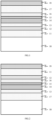
- FIG.1 to 3 illustrate examples of a stack according to the invention.
- the stack successively comprises, from the substrate 10, a first oxide-based dielectric layer 11, an oxygen-donating layer 12, a wetting layer 13, a silver layer 14, optionally a blocker layer 15, optionally an adhesion layer 16, a second dielectric layer 17 and optionally a protective layer 18.
- the oxygen-donating layer 12 can be placed between the substrate 10 and the oxide-based dielectric layer 11.
- the stack successively comprises, from the substrate 10, a first dielectric layer 17, a wetting layer 13, a silver layer 14, optionally a blocker layer 15, optionally an adhesion layer 16, an oxygen 12, a second oxide-based dielectric layer 11 and optionally a protective layer 18.
- the oxygen-donating layer 12 can be placed above the second oxide-based dielectric layer 11 or between the second oxide-based dielectric layer 11 and the optional protective layer 18.
- the stack successively comprises, starting from the substrate 10, a first oxide-based dielectric layer 11a, a first oxygen-donating layer 12a, a wetting layer 13, a silver layer 14, optionally a blocker layer 15 , optionally an adhesion layer 16, a second oxygen-donating layer 12b, a second oxide-based dielectric layer 11b and optionally a protective layer 18.
- the first oxygen-donating layer 12a can be placed between the substrate 10 and the first oxide-based dielectric layer 11a, and/or the second oxygen donor layer 12b can be arranged above of the second oxide-based dielectric layer 11b or between the second oxide-based dielectric layer 11b and the optional protective layer 18.
- the method according to the invention also comprises a step of heat treatment using a laser.
- This heat treatment makes it possible to provide sufficient energy to promote the crystallization of the thin layer of silver, by a physico-chemical mechanism of crystal growth around seeds already present in the layer, while remaining in the solid phase. Promoting the crystallization of the silver layer can in particular result in a disappearance of any amorphous phase residues and/or in an increase in the size of the coherent diffraction domains and/or in a decrease in the density of point defects (vacancies, interstitials) or surface or volume defects such as than twins.
- the method according to the invention has the advantage of heating only the low-emissivity stack, without significant heating of the entire substrate. It is thus no longer necessary to carry out a slow and controlled cooling of the substrate before cutting or storing the glass.
- the use of laser radiation has the advantage of obtaining temperatures generally lower than 100°C, and often even lower than 50°C at the level of the face opposite the first face of the substrate (i.e. say at the level of the uncoated face).
- This particularly advantageous characteristic is due to the fact that the heat exchange coefficient is very high, typically greater than 400 W/(m 2 .s).
- the surface power of the laser radiation at the level of the stack to be treated is even preferably greater than or equal to 10, or even 20 or 30 kW/cm 2 .
- each point of the stack is preferably subjected to the treatment according to the invention (and in particular brought to a temperature greater than or equal to 300° C.) for a duration generally less than or equal to 1 second, or even 0.5 second.
- the part of the glass situated at 0.5 mm from the thin layer does not generally undergo temperatures above 100° C.
- the temperature of the face of the substrate opposite the face treated with the at least one laser radiation preferably does not exceed 100° C., in particular 50° C. and even 30° C. during the heat treatment.
- the laser can thus be integrated into a layer deposition line, for example a magnetic field-assisted sputtering deposition line (magnetron process).
- the line generally includes substrate handling devices, a deposition installation, optical control devices, stacking devices.
- the substrates pass, for example on conveyor rollers, successively in front of each device or each installation.
- the laser is preferably located just after the layer deposition installation, for example at the outlet of the deposition installation.
- the coated substrate can thus be treated in line after the deposition of layers, at the exit from the deposition installation and before the optical control devices, or after the optical control devices and before the substrate stacking devices. It is also possible in certain cases to carry out the heat treatment according to the invention within the vacuum deposition chamber itself.
- the laser is then integrated into the deposition installation. For example, the laser can be introduced into one of the chambers of a sputtering deposition installation.
- the recovery processes may however have an interest in cases where the implementation of the heat treatment according to the invention is carried out in a place different from that where the deposition is carried out, for example in a place where the transformation of the glass is carried out.
- the radiation device can therefore be integrated into lines other than the layer deposition line. It can for example be integrated into a production line for multiple glazing (double or triple glazing in particular), or into a production line for laminated glazing.
- the heat treatment according to the invention is preferably carried out before the production of the multiple or laminated glazing.
- the laser radiation preferably comes from at least one laser beam forming a line (called “laser line” in the remainder of the text) which simultaneously irradiates the entire width of the substrate.
- the line laser beam can in particular be obtained using optical focusing systems.
- the laser line is generally obtained by combining several elementary laser lines.
- the thickness of the elementary laser lines is preferably between 0.01 and 1 mm. Their length is typically between 5 mm and 1 m.
- the elementary laser lines are generally juxtaposed side by side to form a single laser line so that the entire surface of the stack is treated.
- Each elementary laser line is preferably arranged perpendicular to the running direction of the substrate.
- the laser sources are typically laser diodes or fiber lasers, in particular fiber, diode or disc lasers.
- Laser diodes make it possible to economically achieve high power densities with respect to the electric power supply, for a small footprint.
- the bulk of fiber lasers is even more reduced, and the linear power obtained can be even higher, for a higher cost however.
- fiber lasers is meant lasers in which the place of generation of the laser radiation is spatially offset with respect to its place of delivery, the laser radiation being delivered by means of at least one optical fiber.
- the laser radiation is generated in a resonant cavity in which the emitting medium is located, which is in the form of a disc, for example a thin disc (about 0.1 mm thick) in Yb:YAG.
- the radiation thus generated is coupled into at least one optical fiber directed towards the place of treatment.
- the laser can also be fiber, in the sense that the amplification medium is itself an optical fiber.
- Fiber or disc lasers are preferably optically pumped using laser diodes.
- the radiation from the laser sources is preferably continuous.
- the wavelength of the laser radiation is preferably within a range ranging from 500 to 1300 nm, in particular from 800 to 1100 nm.
- Power laser diodes emitting at one or more wavelengths chosen from 808 nm, 880 nm, 915 nm, 940 nm or 980 nm have proved to be particularly well suited.
- the treatment wavelength is for example 1030 nm (emission wavelength for a Yb:YAG laser).
- the treatment wavelength is typically 1070 nm.
- the absorption of the stack at the wavelength of the laser radiation is greater than or equal to 5%, preferably greater than 10% or 15%, or even greater than 20% or even 30%.
- the absorption is defined as being equal to the value of 100% from which the transmission and the reflection of the layer are subtracted.
- the running speed that is to say the difference between the respective speeds of the substrate and of the laser, is greater than or equal to 1 m/min, or even greater than 2, 3, 4 or 5 m/min , or even advantageously greater than or equal to 8 or 10 m/min, in order to ensure a high processing speed.
- the substrate can be set in motion using any mechanical conveying means, for example using strips, rollers, translation plates.
- the conveying system makes it possible to control and regulate the speed of movement. If the substrate is made of flexible polymeric organic material, the movement can be carried out using a film advance system in the form of a succession of rollers.
- the substrate and of the laser are of course possible, as long as the surface of the substrate can be suitably irradiated.
- the substrate will most generally be arranged horizontally, but it can also be arranged vertically, or at any possible inclination.
- the laser is generally arranged so as to irradiate the upper face of the substrate.
- the laser can also irradiate the underside of the substrate.
- the substrate support system possibly the substrate conveying system when the latter is in motion, must allow the radiation to pass into the zone to be irradiated. This is the case, for example, when conveying rollers are used: the rollers being separate, it is possible to place the laser in a zone situated between two successive rollers.
- the present invention also relates to a material comprising a substrate coated with a low-emissivity coating as described above.
- the material according to the invention is capable of being obtained by the method according to the invention.
- the material according to the invention is preferably incorporated into a glazing.
- the present invention therefore also relates to a glazing comprising a material comprising a substrate coated with a low-emissivity coating as described above.
- the glazing may be single or multiple (in particular double or triple), in the sense that it may comprise several sheets of glass providing a space filled with gas.
- the glazing may also be laminated and/or tempered and/or hardened and/or curved.
- a clear glass substrate 4 mm thick marketed under the name SGG Planilux by the applicant are deposited various low-emissivity stacks. All the stacks are deposited, in a known manner, on a cathode sputtering line (magnetron process) in which the substrate passes under different targets.
- Table 1 indicates for each stack tested the physical thickness of the layers, expressed in nm.
- the first line corresponds to the layer furthest from the substrate, in contact with the free air.
- Sample C1 comprises a first dielectric layer of standard titanium oxide TiO 2 while samples C2 and I1 comprise a first dielectric layer of under-oxidized titanium oxide TiO x .
- Sample II further comprises an oxygen-donating layer of mixed tin and zinc oxide SnZnO between the first dielectric layer and the wetting layer of zinc oxide.
- Table 2 summarizes the deposition parameters used for the different layers.
- Layer Target employed Deposition pressure Gas If 3 N 4 If: Al 8% 1.5 ⁇ bar Ar 22 sccm / N 2 22 sccm TiO 2 TiO x underoxidized 1.5 ⁇ bar Ar 30 sccm / O 2 6 sccm TiO x TiO x underoxidized 1.5 ⁇ bar Ar 30 sccm ZnO:Al AZO 2% Al 2 O 3 1.5 ⁇ bar Ar 20 sccm / O 2 2sccm You You 8 ⁇ bar Ar 180 sccm Ag Ag 8 ⁇ bar Ar 180 sccm SnZnO SnZn 60/40wt% 1.5 ⁇ bar Ar 12 sccm / O 2 19 sccm
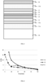
- the samples are treated using a line laser, obtained by juxtaposing several elementary lines, emitting 50% 915 nm 50% 980 nm radiation with a power of 56 kW/cm 2 , against which the coated substrate comes to scroll in translation.
- the samples were processed at different frame rates.
- the square resistance was measured before and after heat treatment.
- the square resistance (Rsq) was measured by a non-contact measurement by induction using an SRM-12 device marketed by Nagy.
- FIG.4 shows for each sample the squared resistance gain (G) of the stack after heat treatment as a function of the treatment speed (V).
- G squared resistance gain
- V treatment speed
- Table 3 summarizes the characteristics of the samples obtained for treatment speeds corresponding to the optimal conditions for each of the samples, that is to say conferring the best compromise between the gain of high square resistance and low residual absorption (light absorption after treatment thermal).
- the light absorption was measured according to the ISO 9050:2003 standard using a CM-3700d spectrophotometer marketed by Konika-Minolta.
- Table 3 Sample C1 C2 I1 Processing speed (m/min) 4 10 8 Forward Rsp ( ⁇ /sq) 4.33 3.78 3.69 Rsp after ( ⁇ /sq) 3.55 3.65 3.02 Gain (%) 18.0 3.44 18.2 Residual absorption (%) 6.54 11.1 7.26
Landscapes
- Chemical & Material Sciences (AREA)
- Life Sciences & Earth Sciences (AREA)
- Engineering & Computer Science (AREA)
- Chemical Kinetics & Catalysis (AREA)
- General Chemical & Material Sciences (AREA)
- Geochemistry & Mineralogy (AREA)
- Materials Engineering (AREA)
- Organic Chemistry (AREA)
- Surface Treatment Of Glass (AREA)
- Laminated Bodies (AREA)
- Insulating Bodies (AREA)
- Physical Vapour Deposition (AREA)
Applications Claiming Priority (2)
| Application Number | Priority Date | Filing Date | Title |
|---|---|---|---|
| FR1659029A FR3056580B1 (fr) | 2016-09-26 | 2016-09-26 | Substrat revetu d'un revetement bas-emissif |
| PCT/FR2017/052570 WO2018055311A1 (fr) | 2016-09-26 | 2017-09-25 | Substrat revetu d'un revetement bas-emissif |
Publications (3)
| Publication Number | Publication Date |
|---|---|
| EP3515872A1 EP3515872A1 (fr) | 2019-07-31 |
| EP3515872C0 EP3515872C0 (fr) | 2023-06-07 |
| EP3515872B1 true EP3515872B1 (fr) | 2023-06-07 |
Family
ID=57750113
Family Applications (1)
| Application Number | Title | Priority Date | Filing Date |
|---|---|---|---|
| EP17780504.1A Active EP3515872B1 (fr) | 2016-09-26 | 2017-09-25 | Substrat revetu d'un revetement bas-emissif |
Country Status (9)
| Country | Link |
|---|---|
| US (1) | US20200017404A1 (pt) |
| EP (1) | EP3515872B1 (pt) |
| JP (1) | JP2019530595A (pt) |
| KR (1) | KR20190060772A (pt) |
| CN (1) | CN109790067A (pt) |
| BR (1) | BR112019005835A2 (pt) |
| FR (1) | FR3056580B1 (pt) |
| PL (1) | PL3515872T3 (pt) |
| WO (1) | WO2018055311A1 (pt) |
Families Citing this family (3)
| Publication number | Priority date | Publication date | Assignee | Title |
|---|---|---|---|---|
| EP3680437B1 (en) * | 2017-09-08 | 2023-10-04 | LG Hausys, Ltd. | Functional building material for door and window |
| US10822270B2 (en) | 2018-08-01 | 2020-11-03 | Guardian Glass, LLC | Coated article including ultra-fast laser treated silver-inclusive layer in low-emissivity thin film coating, and/or method of making the same |
| KR102680655B1 (ko) * | 2021-12-21 | 2024-07-02 | 엠에스웨이 주식회사 | 저저항 도전성 박막 및 그 제조방법 |
Family Cites Families (15)
| Publication number | Priority date | Publication date | Assignee | Title |
|---|---|---|---|---|
| FR2859721B1 (fr) * | 2003-09-17 | 2006-08-25 | Saint Gobain | Substrat transparent muni d'un empilement de couches minces pour un blindage electromagnetique |
| FR2898123B1 (fr) * | 2006-03-06 | 2008-12-05 | Saint Gobain | Substrat muni d'un empilement a proprietes thermiques |
| US8409717B2 (en) * | 2008-04-21 | 2013-04-02 | Guardian Industries Corp. | Coated article with IR reflecting layer and method of making same |
| FR2946639B1 (fr) * | 2009-06-12 | 2011-07-15 | Saint Gobain | Procede de depot de couche mince et produit obtenu. |
| FR2969391B1 (fr) * | 2010-12-17 | 2013-07-05 | Saint Gobain | Procédé de fabrication d'un dispositif oled |
| FR2981346B1 (fr) * | 2011-10-18 | 2014-01-24 | Saint Gobain | Procede de traitement thermique de couches d'argent |
| CN102529210B (zh) * | 2011-12-19 | 2014-10-15 | 林嘉宏 | 具有保护膜层的镀膜玻璃及其制备方法 |
| FR2989388B1 (fr) * | 2012-04-17 | 2019-10-18 | Saint-Gobain Glass France | Procede d'obtention d'un substrat muni d'un revetement |
| US9919959B2 (en) * | 2012-05-31 | 2018-03-20 | Guardian Glass, LLC | Window with UV-treated low-E coating and method of making same |
| FR3002768B1 (fr) * | 2013-03-01 | 2015-02-20 | Saint Gobain | Procede de traitement thermique d'un revetement |
| EA029123B1 (ru) * | 2013-05-30 | 2018-02-28 | Агк Гласс Юроп | Солнцезащитное остекление |
| GB201314699D0 (en) * | 2013-08-16 | 2013-10-02 | Pilkington Group Ltd | Heat treatable coated glass pane |
| FR3012133B1 (fr) * | 2013-10-17 | 2021-01-01 | Saint Gobain | Procede d'obtention d'un substrat revetu par un empilement comprenant une couche d'oxyde transparent conducteur |
| FR3013348B1 (fr) * | 2013-11-15 | 2021-01-01 | Saint Gobain | Vitrage comprenant un substrat revetu d'un empilement comprenant une couche fonctionnelle a base d'argent et une sous-couche de blocage epaisse de tiox |
| CN104230182A (zh) * | 2014-09-28 | 2014-12-24 | 中国建材国际工程集团有限公司 | 高透过率可钢化低辐射镀膜玻璃的制备方法 |
-
2016
- 2016-09-26 FR FR1659029A patent/FR3056580B1/fr active Active
-
2017
- 2017-09-25 KR KR1020197008648A patent/KR20190060772A/ko not_active Application Discontinuation
- 2017-09-25 BR BR112019005835A patent/BR112019005835A2/pt not_active Application Discontinuation
- 2017-09-25 WO PCT/FR2017/052570 patent/WO2018055311A1/fr active Application Filing
- 2017-09-25 JP JP2019516180A patent/JP2019530595A/ja active Pending
- 2017-09-25 PL PL17780504.1T patent/PL3515872T3/pl unknown
- 2017-09-25 CN CN201780059379.5A patent/CN109790067A/zh active Pending
- 2017-09-25 US US16/335,563 patent/US20200017404A1/en not_active Abandoned
- 2017-09-25 EP EP17780504.1A patent/EP3515872B1/fr active Active
Also Published As
| Publication number | Publication date |
|---|---|
| EP3515872A1 (fr) | 2019-07-31 |
| FR3056580B1 (fr) | 2021-02-12 |
| PL3515872T3 (pl) | 2023-08-21 |
| BR112019005835A2 (pt) | 2019-06-18 |
| EP3515872C0 (fr) | 2023-06-07 |
| JP2019530595A (ja) | 2019-10-24 |
| KR20190060772A (ko) | 2019-06-03 |
| CN109790067A (zh) | 2019-05-21 |
| WO2018055311A1 (fr) | 2018-03-29 |
| US20200017404A1 (en) | 2020-01-16 |
| FR3056580A1 (fr) | 2018-03-30 |
Similar Documents
| Publication | Publication Date | Title |
|---|---|---|
| EP2440503B1 (fr) | Procede de depot de couche mince et produit obtenu | |
| EP2683669B1 (fr) | Procede d'obtention d'un substrat muni d'un revêtement | |
| CA2806269C (fr) | Procede d'obtention d'un materiau comprenant un substrat muni d'un revetement | |
| EP2438024B1 (fr) | Procede de depot de couche mince | |
| EP2652812B1 (fr) | Procede de fabrication d'un dispositif oled | |
| CA2774937C (fr) | Procede de depot de couche mince | |
| CA2865696C (fr) | Vitrage anticondensation | |
| WO2005000758A2 (fr) | Substrat revetu d’une couche dielectrique et procede et installation pour sa fabrication | |
| CA2902850A1 (fr) | Procede de traitement thermique d'un revetement | |
| EP3515872B1 (fr) | Substrat revetu d'un revetement bas-emissif | |
| WO2018055310A1 (fr) | Substrat revêtu d'un revêtement bas-émissif | |
| FR2943050A1 (fr) | Procede de depot de couche mince. | |
| FR2991980A1 (fr) | Procede de depot de couches minces avec etape de traitement sous vide et produit obtenu | |
| WO2017203144A1 (fr) | Procede de depot de couches minces |
Legal Events
| Date | Code | Title | Description |
|---|---|---|---|
| STAA | Information on the status of an ep patent application or granted ep patent |
Free format text: STATUS: UNKNOWN |
|
| STAA | Information on the status of an ep patent application or granted ep patent |
Free format text: STATUS: THE INTERNATIONAL PUBLICATION HAS BEEN MADE |
|
| PUAI | Public reference made under article 153(3) epc to a published international application that has entered the european phase |
Free format text: ORIGINAL CODE: 0009012 |
|
| STAA | Information on the status of an ep patent application or granted ep patent |
Free format text: STATUS: REQUEST FOR EXAMINATION WAS MADE |
|
| 17P | Request for examination filed |
Effective date: 20190426 |
|
| AK | Designated contracting states |
Kind code of ref document: A1 Designated state(s): AL AT BE BG CH CY CZ DE DK EE ES FI FR GB GR HR HU IE IS IT LI LT LU LV MC MK MT NL NO PL PT RO RS SE SI SK SM TR |
|
| AX | Request for extension of the european patent |
Extension state: BA ME |
|
| DAV | Request for validation of the european patent (deleted) | ||
| DAX | Request for extension of the european patent (deleted) | ||
| STAA | Information on the status of an ep patent application or granted ep patent |
Free format text: STATUS: EXAMINATION IS IN PROGRESS |
|
| 17Q | First examination report despatched |
Effective date: 20200128 |
|
| STAA | Information on the status of an ep patent application or granted ep patent |
Free format text: STATUS: EXAMINATION IS IN PROGRESS |
|
| RAP1 | Party data changed (applicant data changed or rights of an application transferred) |
Owner name: SAINT-GOBAIN GLASS FRANCE |
|
| STAA | Information on the status of an ep patent application or granted ep patent |
Free format text: STATUS: EXAMINATION IS IN PROGRESS |
|
| GRAP | Despatch of communication of intention to grant a patent |
Free format text: ORIGINAL CODE: EPIDOSNIGR1 |
|
| STAA | Information on the status of an ep patent application or granted ep patent |
Free format text: STATUS: GRANT OF PATENT IS INTENDED |
|
| INTG | Intention to grant announced |
Effective date: 20230117 |
|
| GRAS | Grant fee paid |
Free format text: ORIGINAL CODE: EPIDOSNIGR3 |
|
| GRAA | (expected) grant |
Free format text: ORIGINAL CODE: 0009210 |
|
| STAA | Information on the status of an ep patent application or granted ep patent |
Free format text: STATUS: THE PATENT HAS BEEN GRANTED |
|
| AK | Designated contracting states |
Kind code of ref document: B1 Designated state(s): AL AT BE BG CH CY CZ DE DK EE ES FI FR GB GR HR HU IE IS IT LI LT LU LV MC MK MT NL NO PL PT RO RS SE SI SK SM TR |
|
| REG | Reference to a national code |
Ref country code: GB Ref legal event code: FG4D Free format text: NOT ENGLISH |
|
| REG | Reference to a national code |
Ref country code: CH Ref legal event code: EP Ref country code: AT Ref legal event code: REF Ref document number: 1574614 Country of ref document: AT Kind code of ref document: T Effective date: 20230615 |
|
| REG | Reference to a national code |
Ref country code: DE Ref legal event code: R096 Ref document number: 602017069686 Country of ref document: DE |
|
| U01 | Request for unitary effect filed |
Effective date: 20230623 |
|
| U07 | Unitary effect registered |
Designated state(s): AT BE BG DE DK EE FI FR IT LT LU LV MT NL PT SE SI Effective date: 20230704 |
|
| REG | Reference to a national code |
Ref country code: LT Ref legal event code: MG9D |
|
| PG25 | Lapsed in a contracting state [announced via postgrant information from national office to epo] |
Ref country code: NO Free format text: LAPSE BECAUSE OF FAILURE TO SUBMIT A TRANSLATION OF THE DESCRIPTION OR TO PAY THE FEE WITHIN THE PRESCRIBED TIME-LIMIT Effective date: 20230907 Ref country code: ES Free format text: LAPSE BECAUSE OF FAILURE TO SUBMIT A TRANSLATION OF THE DESCRIPTION OR TO PAY THE FEE WITHIN THE PRESCRIBED TIME-LIMIT Effective date: 20230607 |
|
| PGFP | Annual fee paid to national office [announced via postgrant information from national office to epo] |
Ref country code: TR Payment date: 20230922 Year of fee payment: 7 Ref country code: GB Payment date: 20230803 Year of fee payment: 7 |
|
| U20 | Renewal fee paid [unitary effect] |
Year of fee payment: 7 Effective date: 20231016 |
|
| PG25 | Lapsed in a contracting state [announced via postgrant information from national office to epo] |
Ref country code: RS Free format text: LAPSE BECAUSE OF FAILURE TO SUBMIT A TRANSLATION OF THE DESCRIPTION OR TO PAY THE FEE WITHIN THE PRESCRIBED TIME-LIMIT Effective date: 20230607 Ref country code: HR Free format text: LAPSE BECAUSE OF FAILURE TO SUBMIT A TRANSLATION OF THE DESCRIPTION OR TO PAY THE FEE WITHIN THE PRESCRIBED TIME-LIMIT Effective date: 20230607 Ref country code: GR Free format text: LAPSE BECAUSE OF FAILURE TO SUBMIT A TRANSLATION OF THE DESCRIPTION OR TO PAY THE FEE WITHIN THE PRESCRIBED TIME-LIMIT Effective date: 20230908 |
|
| PGFP | Annual fee paid to national office [announced via postgrant information from national office to epo] |
Ref country code: PL Payment date: 20230804 Year of fee payment: 7 |
|
| PG25 | Lapsed in a contracting state [announced via postgrant information from national office to epo] |
Ref country code: SK Free format text: LAPSE BECAUSE OF FAILURE TO SUBMIT A TRANSLATION OF THE DESCRIPTION OR TO PAY THE FEE WITHIN THE PRESCRIBED TIME-LIMIT Effective date: 20230607 |
|
| PG25 | Lapsed in a contracting state [announced via postgrant information from national office to epo] |
Ref country code: IS Free format text: LAPSE BECAUSE OF FAILURE TO SUBMIT A TRANSLATION OF THE DESCRIPTION OR TO PAY THE FEE WITHIN THE PRESCRIBED TIME-LIMIT Effective date: 20231007 |
|
| PG25 | Lapsed in a contracting state [announced via postgrant information from national office to epo] |
Ref country code: SM Free format text: LAPSE BECAUSE OF FAILURE TO SUBMIT A TRANSLATION OF THE DESCRIPTION OR TO PAY THE FEE WITHIN THE PRESCRIBED TIME-LIMIT Effective date: 20230607 Ref country code: SK Free format text: LAPSE BECAUSE OF FAILURE TO SUBMIT A TRANSLATION OF THE DESCRIPTION OR TO PAY THE FEE WITHIN THE PRESCRIBED TIME-LIMIT Effective date: 20230607 Ref country code: RO Free format text: LAPSE BECAUSE OF FAILURE TO SUBMIT A TRANSLATION OF THE DESCRIPTION OR TO PAY THE FEE WITHIN THE PRESCRIBED TIME-LIMIT Effective date: 20230607 Ref country code: IS Free format text: LAPSE BECAUSE OF FAILURE TO SUBMIT A TRANSLATION OF THE DESCRIPTION OR TO PAY THE FEE WITHIN THE PRESCRIBED TIME-LIMIT Effective date: 20231007 Ref country code: CZ Free format text: LAPSE BECAUSE OF FAILURE TO SUBMIT A TRANSLATION OF THE DESCRIPTION OR TO PAY THE FEE WITHIN THE PRESCRIBED TIME-LIMIT Effective date: 20230607 |
|
| REG | Reference to a national code |
Ref country code: DE Ref legal event code: R097 Ref document number: 602017069686 Country of ref document: DE |
|
| PLBE | No opposition filed within time limit |
Free format text: ORIGINAL CODE: 0009261 |
|
| STAA | Information on the status of an ep patent application or granted ep patent |
Free format text: STATUS: NO OPPOSITION FILED WITHIN TIME LIMIT |
|
| REG | Reference to a national code |
Ref country code: CH Ref legal event code: PL |
|
| 26N | No opposition filed |
Effective date: 20240308 |
|
| PG25 | Lapsed in a contracting state [announced via postgrant information from national office to epo] |
Ref country code: MC Free format text: LAPSE BECAUSE OF FAILURE TO SUBMIT A TRANSLATION OF THE DESCRIPTION OR TO PAY THE FEE WITHIN THE PRESCRIBED TIME-LIMIT Effective date: 20230607 |
|
| REG | Reference to a national code |
Ref country code: IE Ref legal event code: MM4A |
|
| PG25 | Lapsed in a contracting state [announced via postgrant information from national office to epo] |
Ref country code: IE Free format text: LAPSE BECAUSE OF NON-PAYMENT OF DUE FEES Effective date: 20230925 |
|
| PG25 | Lapsed in a contracting state [announced via postgrant information from national office to epo] |
Ref country code: CH Free format text: LAPSE BECAUSE OF NON-PAYMENT OF DUE FEES Effective date: 20230930 |
|
| PG25 | Lapsed in a contracting state [announced via postgrant information from national office to epo] |
Ref country code: IE Free format text: LAPSE BECAUSE OF NON-PAYMENT OF DUE FEES Effective date: 20230925 Ref country code: CH Free format text: LAPSE BECAUSE OF NON-PAYMENT OF DUE FEES Effective date: 20230930 |