EP3515872B1 - Substrate coated with a low-emissivity coating - Google Patents
Substrate coated with a low-emissivity coating Download PDFInfo
- Publication number
- EP3515872B1 EP3515872B1 EP17780504.1A EP17780504A EP3515872B1 EP 3515872 B1 EP3515872 B1 EP 3515872B1 EP 17780504 A EP17780504 A EP 17780504A EP 3515872 B1 EP3515872 B1 EP 3515872B1
- Authority
- EP
- European Patent Office
- Prior art keywords
- layer
- oxide
- dielectric layer
- substrate
- oxygen
- Prior art date
- Legal status (The legal status is an assumption and is not a legal conclusion. Google has not performed a legal analysis and makes no representation as to the accuracy of the status listed.)
- Active
Links
- 239000000758 substrate Substances 0.000 title claims description 93
- 238000000576 coating method Methods 0.000 title description 9
- 239000011248 coating agent Substances 0.000 title description 7
- XLOMVQKBTHCTTD-UHFFFAOYSA-N Zinc monoxide Chemical compound [Zn]=O XLOMVQKBTHCTTD-UHFFFAOYSA-N 0.000 claims description 158
- 239000011787 zinc oxide Substances 0.000 claims description 79
- 239000010936 titanium Substances 0.000 claims description 54
- BQCADISMDOOEFD-UHFFFAOYSA-N Silver Chemical compound [Ag] BQCADISMDOOEFD-UHFFFAOYSA-N 0.000 claims description 44
- 229910052709 silver Inorganic materials 0.000 claims description 44
- 239000004332 silver Substances 0.000 claims description 44
- OGIDPMRJRNCKJF-UHFFFAOYSA-N titanium oxide Inorganic materials [Ti]=O OGIDPMRJRNCKJF-UHFFFAOYSA-N 0.000 claims description 43
- 238000000034 method Methods 0.000 claims description 37
- 230000008569 process Effects 0.000 claims description 28
- 238000009736 wetting Methods 0.000 claims description 28
- GWEVSGVZZGPLCZ-UHFFFAOYSA-N Titan oxide Chemical compound O=[Ti]=O GWEVSGVZZGPLCZ-UHFFFAOYSA-N 0.000 claims description 26
- 239000011521 glass Substances 0.000 claims description 26
- 229910003087 TiOx Inorganic materials 0.000 claims description 25
- HLLICFJUWSZHRJ-UHFFFAOYSA-N tioxidazole Chemical compound CCCOC1=CC=C2N=C(NC(=O)OC)SC2=C1 HLLICFJUWSZHRJ-UHFFFAOYSA-N 0.000 claims description 25
- 230000005855 radiation Effects 0.000 claims description 19
- 239000000463 material Substances 0.000 claims description 15
- 238000011282 treatment Methods 0.000 claims description 10
- ATJFFYVFTNAWJD-UHFFFAOYSA-N Tin Chemical compound [Sn] ATJFFYVFTNAWJD-UHFFFAOYSA-N 0.000 claims description 9
- RTAQQCXQSZGOHL-UHFFFAOYSA-N Titanium Chemical compound [Ti] RTAQQCXQSZGOHL-UHFFFAOYSA-N 0.000 claims description 6
- 239000002241 glass-ceramic Substances 0.000 claims description 5
- 239000010955 niobium Substances 0.000 claims description 3
- GUCVJGMIXFAOAE-UHFFFAOYSA-N niobium atom Chemical compound [Nb] GUCVJGMIXFAOAE-UHFFFAOYSA-N 0.000 claims description 3
- 229910052814 silicon oxide Inorganic materials 0.000 claims description 3
- 239000011701 zinc Substances 0.000 claims description 3
- XUIMIQQOPSSXEZ-UHFFFAOYSA-N Silicon Chemical compound [Si] XUIMIQQOPSSXEZ-UHFFFAOYSA-N 0.000 claims description 2
- HCHKCACWOHOZIP-UHFFFAOYSA-N Zinc Chemical compound [Zn] HCHKCACWOHOZIP-UHFFFAOYSA-N 0.000 claims description 2
- CPLXHLVBOLITMK-UHFFFAOYSA-N magnesium oxide Inorganic materials [Mg]=O CPLXHLVBOLITMK-UHFFFAOYSA-N 0.000 claims description 2
- 239000000395 magnesium oxide Substances 0.000 claims description 2
- AXZKOIWUVFPNLO-UHFFFAOYSA-N magnesium;oxygen(2-) Chemical compound [O-2].[Mg+2] AXZKOIWUVFPNLO-UHFFFAOYSA-N 0.000 claims description 2
- 229910000484 niobium oxide Inorganic materials 0.000 claims description 2
- 239000010703 silicon Substances 0.000 claims description 2
- 229910052725 zinc Inorganic materials 0.000 claims description 2
- 229920000620 organic polymer Polymers 0.000 claims 2
- 239000002861 polymer material Substances 0.000 claims 2
- 230000003247 decreasing effect Effects 0.000 claims 1
- 239000010410 layer Substances 0.000 description 265
- QVGXLLKOCUKJST-UHFFFAOYSA-N atomic oxygen Chemical compound [O] QVGXLLKOCUKJST-UHFFFAOYSA-N 0.000 description 22
- 229910052760 oxygen Inorganic materials 0.000 description 22
- 239000001301 oxygen Substances 0.000 description 22
- 229910052581 Si3N4 Inorganic materials 0.000 description 19
- 238000000151 deposition Methods 0.000 description 19
- 230000008021 deposition Effects 0.000 description 18
- 238000010438 heat treatment Methods 0.000 description 18
- 229910010413 TiO 2 Inorganic materials 0.000 description 15
- 238000010521 absorption reaction Methods 0.000 description 9
- 238000002425 crystallisation Methods 0.000 description 8
- 230000008025 crystallization Effects 0.000 description 8
- 238000009434 installation Methods 0.000 description 8
- 239000011241 protective layer Substances 0.000 description 8
- 239000000835 fiber Substances 0.000 description 7
- 229910052751 metal Inorganic materials 0.000 description 7
- 239000002184 metal Substances 0.000 description 7
- 230000005540 biological transmission Effects 0.000 description 6
- 238000005224 laser annealing Methods 0.000 description 6
- 230000003287 optical effect Effects 0.000 description 6
- 238000012545 processing Methods 0.000 description 6
- 238000004519 manufacturing process Methods 0.000 description 5
- 150000004767 nitrides Chemical class 0.000 description 5
- 239000011368 organic material Substances 0.000 description 5
- 238000004544 sputter deposition Methods 0.000 description 5
- 229910001887 tin oxide Inorganic materials 0.000 description 5
- PXHVJJICTQNCMI-UHFFFAOYSA-N Nickel Chemical compound [Ni] PXHVJJICTQNCMI-UHFFFAOYSA-N 0.000 description 4
- 230000008901 benefit Effects 0.000 description 4
- 230000014509 gene expression Effects 0.000 description 4
- 230000033001 locomotion Effects 0.000 description 4
- 229910052719 titanium Inorganic materials 0.000 description 4
- 229910052782 aluminium Inorganic materials 0.000 description 3
- XAGFODPZIPBFFR-UHFFFAOYSA-N aluminium Chemical compound [Al] XAGFODPZIPBFFR-UHFFFAOYSA-N 0.000 description 3
- 230000000694 effects Effects 0.000 description 3
- 239000007789 gas Substances 0.000 description 3
- 239000013307 optical fiber Substances 0.000 description 3
- HQVNEWCFYHHQES-UHFFFAOYSA-N silicon nitride Chemical compound N12[Si]34N5[Si]62N3[Si]51N64 HQVNEWCFYHHQES-UHFFFAOYSA-N 0.000 description 3
- XOLBLPGZBRYERU-UHFFFAOYSA-N tin dioxide Chemical compound O=[Sn]=O XOLBLPGZBRYERU-UHFFFAOYSA-N 0.000 description 3
- 238000013519 translation Methods 0.000 description 3
- VYZAMTAEIAYCRO-UHFFFAOYSA-N Chromium Chemical compound [Cr] VYZAMTAEIAYCRO-UHFFFAOYSA-N 0.000 description 2
- 229910045601 alloy Inorganic materials 0.000 description 2
- 239000000956 alloy Substances 0.000 description 2
- 239000011651 chromium Substances 0.000 description 2
- 229910052804 chromium Inorganic materials 0.000 description 2
- 230000001427 coherent effect Effects 0.000 description 2
- 230000007547 defect Effects 0.000 description 2
- 230000031700 light absorption Effects 0.000 description 2
- 229910044991 metal oxide Inorganic materials 0.000 description 2
- 150000004706 metal oxides Chemical class 0.000 description 2
- 150000002739 metals Chemical class 0.000 description 2
- 230000005012 migration Effects 0.000 description 2
- 238000013508 migration Methods 0.000 description 2
- 239000000203 mixture Substances 0.000 description 2
- 229910052759 nickel Inorganic materials 0.000 description 2
- 229910000623 nickel–chromium alloy Inorganic materials 0.000 description 2
- 230000003647 oxidation Effects 0.000 description 2
- 238000007254 oxidation reaction Methods 0.000 description 2
- 229920000139 polyethylene terephthalate Polymers 0.000 description 2
- 239000005020 polyethylene terephthalate Substances 0.000 description 2
- 238000011084 recovery Methods 0.000 description 2
- 239000000126 substance Substances 0.000 description 2
- 229910018072 Al 2 O 3 Inorganic materials 0.000 description 1
- 229910000906 Bronze Inorganic materials 0.000 description 1
- 229910000990 Ni alloy Inorganic materials 0.000 description 1
- VYPSYNLAJGMNEJ-UHFFFAOYSA-N Silicium dioxide Chemical compound O=[Si]=O VYPSYNLAJGMNEJ-UHFFFAOYSA-N 0.000 description 1
- 229910006404 SnO 2 Inorganic materials 0.000 description 1
- 229910005728 SnZn Inorganic materials 0.000 description 1
- 238000002441 X-ray diffraction Methods 0.000 description 1
- HZEWFHLRYVTOIW-UHFFFAOYSA-N [Ti].[Ni] Chemical compound [Ti].[Ni] HZEWFHLRYVTOIW-UHFFFAOYSA-N 0.000 description 1
- 230000002745 absorbent Effects 0.000 description 1
- 239000002250 absorbent Substances 0.000 description 1
- 239000005407 aluminoborosilicate glass Substances 0.000 description 1
- 230000003321 amplification Effects 0.000 description 1
- 230000008033 biological extinction Effects 0.000 description 1
- 239000005388 borosilicate glass Substances 0.000 description 1
- 239000010974 bronze Substances 0.000 description 1
- 239000002800 charge carrier Substances 0.000 description 1
- 229910052729 chemical element Inorganic materials 0.000 description 1
- 238000006243 chemical reaction Methods 0.000 description 1
- 239000000788 chromium alloy Substances 0.000 description 1
- 238000004140 cleaning Methods 0.000 description 1
- 238000010924 continuous production Methods 0.000 description 1
- 238000001816 cooling Methods 0.000 description 1
- KUNSUQLRTQLHQQ-UHFFFAOYSA-N copper tin Chemical compound [Cu].[Sn] KUNSUQLRTQLHQQ-UHFFFAOYSA-N 0.000 description 1
- 239000013078 crystal Substances 0.000 description 1
- 238000005520 cutting process Methods 0.000 description 1
- 238000005137 deposition process Methods 0.000 description 1
- 230000002542 deteriorative effect Effects 0.000 description 1
- 230000008034 disappearance Effects 0.000 description 1
- 238000006073 displacement reaction Methods 0.000 description 1
- 230000002349 favourable effect Effects 0.000 description 1
- 230000006698 induction Effects 0.000 description 1
- 150000002484 inorganic compounds Chemical class 0.000 description 1
- 229910010272 inorganic material Inorganic materials 0.000 description 1
- 238000005259 measurement Methods 0.000 description 1
- 230000007246 mechanism Effects 0.000 description 1
- 239000006060 molten glass Substances 0.000 description 1
- 229910001000 nickel titanium Inorganic materials 0.000 description 1
- 229910052758 niobium Inorganic materials 0.000 description 1
- 230000006911 nucleation Effects 0.000 description 1
- 238000010899 nucleation Methods 0.000 description 1
- 238000003199 nucleic acid amplification method Methods 0.000 description 1
- 230000001590 oxidative effect Effects 0.000 description 1
- 239000012071 phase Substances 0.000 description 1
- 229920003229 poly(methyl methacrylate) Polymers 0.000 description 1
- 239000004417 polycarbonate Substances 0.000 description 1
- 229920000515 polycarbonate Polymers 0.000 description 1
- -1 polyethylene terephthalate Polymers 0.000 description 1
- 239000004926 polymethyl methacrylate Substances 0.000 description 1
- 230000001737 promoting effect Effects 0.000 description 1
- 238000005086 pumping Methods 0.000 description 1
- 230000009467 reduction Effects 0.000 description 1
- 238000005096 rolling process Methods 0.000 description 1
- 150000003378 silver Chemical class 0.000 description 1
- 239000005361 soda-lime glass Substances 0.000 description 1
- 239000007790 solid phase Substances 0.000 description 1
- 230000009466 transformation Effects 0.000 description 1
- 238000001771 vacuum deposition Methods 0.000 description 1
Images
Classifications
-
- C—CHEMISTRY; METALLURGY
- C03—GLASS; MINERAL OR SLAG WOOL
- C03C—CHEMICAL COMPOSITION OF GLASSES, GLAZES OR VITREOUS ENAMELS; SURFACE TREATMENT OF GLASS; SURFACE TREATMENT OF FIBRES OR FILAMENTS MADE FROM GLASS, MINERALS OR SLAGS; JOINING GLASS TO GLASS OR OTHER MATERIALS
- C03C17/00—Surface treatment of glass, not in the form of fibres or filaments, by coating
- C03C17/34—Surface treatment of glass, not in the form of fibres or filaments, by coating with at least two coatings having different compositions
- C03C17/36—Surface treatment of glass, not in the form of fibres or filaments, by coating with at least two coatings having different compositions at least one coating being a metal
- C03C17/3602—Surface treatment of glass, not in the form of fibres or filaments, by coating with at least two coatings having different compositions at least one coating being a metal the metal being present as a layer
- C03C17/3626—Surface treatment of glass, not in the form of fibres or filaments, by coating with at least two coatings having different compositions at least one coating being a metal the metal being present as a layer one layer at least containing a nitride, oxynitride, boronitride or carbonitride
-
- C—CHEMISTRY; METALLURGY
- C03—GLASS; MINERAL OR SLAG WOOL
- C03C—CHEMICAL COMPOSITION OF GLASSES, GLAZES OR VITREOUS ENAMELS; SURFACE TREATMENT OF GLASS; SURFACE TREATMENT OF FIBRES OR FILAMENTS MADE FROM GLASS, MINERALS OR SLAGS; JOINING GLASS TO GLASS OR OTHER MATERIALS
- C03C17/00—Surface treatment of glass, not in the form of fibres or filaments, by coating
- C03C17/34—Surface treatment of glass, not in the form of fibres or filaments, by coating with at least two coatings having different compositions
- C03C17/36—Surface treatment of glass, not in the form of fibres or filaments, by coating with at least two coatings having different compositions at least one coating being a metal
- C03C17/3602—Surface treatment of glass, not in the form of fibres or filaments, by coating with at least two coatings having different compositions at least one coating being a metal the metal being present as a layer
- C03C17/3644—Surface treatment of glass, not in the form of fibres or filaments, by coating with at least two coatings having different compositions at least one coating being a metal the metal being present as a layer the metal being silver
-
- C—CHEMISTRY; METALLURGY
- C03—GLASS; MINERAL OR SLAG WOOL
- C03C—CHEMICAL COMPOSITION OF GLASSES, GLAZES OR VITREOUS ENAMELS; SURFACE TREATMENT OF GLASS; SURFACE TREATMENT OF FIBRES OR FILAMENTS MADE FROM GLASS, MINERALS OR SLAGS; JOINING GLASS TO GLASS OR OTHER MATERIALS
- C03C17/00—Surface treatment of glass, not in the form of fibres or filaments, by coating
- C03C17/34—Surface treatment of glass, not in the form of fibres or filaments, by coating with at least two coatings having different compositions
- C03C17/36—Surface treatment of glass, not in the form of fibres or filaments, by coating with at least two coatings having different compositions at least one coating being a metal
- C03C17/3602—Surface treatment of glass, not in the form of fibres or filaments, by coating with at least two coatings having different compositions at least one coating being a metal the metal being present as a layer
- C03C17/3652—Surface treatment of glass, not in the form of fibres or filaments, by coating with at least two coatings having different compositions at least one coating being a metal the metal being present as a layer the coating stack containing at least one sacrificial layer to protect the metal from oxidation
-
- C—CHEMISTRY; METALLURGY
- C03—GLASS; MINERAL OR SLAG WOOL
- C03C—CHEMICAL COMPOSITION OF GLASSES, GLAZES OR VITREOUS ENAMELS; SURFACE TREATMENT OF GLASS; SURFACE TREATMENT OF FIBRES OR FILAMENTS MADE FROM GLASS, MINERALS OR SLAGS; JOINING GLASS TO GLASS OR OTHER MATERIALS
- C03C17/00—Surface treatment of glass, not in the form of fibres or filaments, by coating
- C03C17/34—Surface treatment of glass, not in the form of fibres or filaments, by coating with at least two coatings having different compositions
- C03C17/36—Surface treatment of glass, not in the form of fibres or filaments, by coating with at least two coatings having different compositions at least one coating being a metal
- C03C17/3602—Surface treatment of glass, not in the form of fibres or filaments, by coating with at least two coatings having different compositions at least one coating being a metal the metal being present as a layer
- C03C17/3657—Surface treatment of glass, not in the form of fibres or filaments, by coating with at least two coatings having different compositions at least one coating being a metal the metal being present as a layer the multilayer coating having optical properties
- C03C17/366—Low-emissivity or solar control coatings
-
- C—CHEMISTRY; METALLURGY
- C03—GLASS; MINERAL OR SLAG WOOL
- C03C—CHEMICAL COMPOSITION OF GLASSES, GLAZES OR VITREOUS ENAMELS; SURFACE TREATMENT OF GLASS; SURFACE TREATMENT OF FIBRES OR FILAMENTS MADE FROM GLASS, MINERALS OR SLAGS; JOINING GLASS TO GLASS OR OTHER MATERIALS
- C03C17/00—Surface treatment of glass, not in the form of fibres or filaments, by coating
- C03C17/34—Surface treatment of glass, not in the form of fibres or filaments, by coating with at least two coatings having different compositions
- C03C17/36—Surface treatment of glass, not in the form of fibres or filaments, by coating with at least two coatings having different compositions at least one coating being a metal
- C03C17/3602—Surface treatment of glass, not in the form of fibres or filaments, by coating with at least two coatings having different compositions at least one coating being a metal the metal being present as a layer
- C03C17/3681—Surface treatment of glass, not in the form of fibres or filaments, by coating with at least two coatings having different compositions at least one coating being a metal the metal being present as a layer the multilayer coating being used in glazing, e.g. windows or windscreens
-
- C—CHEMISTRY; METALLURGY
- C03—GLASS; MINERAL OR SLAG WOOL
- C03C—CHEMICAL COMPOSITION OF GLASSES, GLAZES OR VITREOUS ENAMELS; SURFACE TREATMENT OF GLASS; SURFACE TREATMENT OF FIBRES OR FILAMENTS MADE FROM GLASS, MINERALS OR SLAGS; JOINING GLASS TO GLASS OR OTHER MATERIALS
- C03C2218/00—Methods for coating glass
- C03C2218/30—Aspects of methods for coating glass not covered above
- C03C2218/32—After-treatment
Definitions
- the invention relates to the field of inorganic thin layers, in particular deposited on glass substrates. It relates more particularly to a process for obtaining a material comprising a substrate coated on at least one face with a stack of low-emissivity thin layers.
- optical properties for example of reflection or absorption of radiation of a range of wavelengths data, particular electrical conduction properties, or even properties related to the ease of cleaning or the possibility for the material to self-clean.
- a plasma is created under a high vacuum in the vicinity of a target comprising the chemical elements to be deposited.
- the active species of the plasma by bombarding the target, tear off said elements, which are deposited on the substrate, forming the desired thin layer.
- This process is said to be “reactive” when the layer consists of a material resulting from a chemical reaction between the elements torn from the target and the gas contained in the plasma.
- the major advantage of this method lies in the possibility of depositing on the same line a very complex stack of layers by successively making the substrate pass under different targets, this generally in a single and same device.
- thin layers are most often based on inorganic compounds: oxides, nitrides, or even metals. Their thickness generally varies from a few nanometers to a few hundred nanometers, hence their qualifier “thin”.
- the thin layers based on metallic silver which have properties of electrical conduction and reflection of infrared radiation, hence their use in solar control glazing, in particular solar protection (aimed at reducing the incoming solar energy) and/or low emissivity (aimed at reducing the amount of energy dissipated outside a building or vehicle).
- the or each layer of silver is generally inserted in a stack of layers.
- the or each silver-based thin layer is generally arranged between two dielectric thin layers based on oxide or nitride (for example TiO 2 , SnO 2 or Si 3N4 ) .
- These layers are respectively called wetting layer and blocker layer.
- WO 2010/142926 describes stacks of low-emission thin layers comprising in particular a silver layer, dielectric layers based on TiO 2 and Si 2 N 3 , a wetting layer based on ZnO and a layer of titanium blocker.
- the silver layers have the particularity of seeing some of their properties improved when they are in an at least partially crystallized state. It is generally sought to increase as much as possible the rate of crystallization of these layers (the mass or volume proportion of crystallized material) and the size of the crystalline grains (or the size of coherent diffraction domains measured by X-ray diffraction methods). It is known in particular that silver layers having a high crystallization rate and consequently a low residual content of nanometric grains have lower emissivity and resistivity as well as higher transmission in the visible than silver layers. mostly nano-crystallized. The electrical conductivity and the low emissivity properties of these layers are thus improved. The increase in the size of the grains is in fact accompanied by a reduction in the grain boundaries, favorable to the mobility of the electric charge carriers.
- the silver layers deposited by the magnetron process are generally mostly or even completely nano-crystallized (the average size of the crystalline grains being less than a few nanometers), and heat treatments prove necessary to obtain the desired crystallization rate or the grain size. desired.
- the thin oxide-based dielectric layers are generally deposited by a reactive magnetron process from a metallic or substoichiometric oxide target in a plasma containing oxygen.
- the process parameters are then generally adjusted so as to obtain the desired oxide in a stoichiometric proportion.
- the deposited oxide layer may have a sub-stoichiometric composition. It was observed that, in this case, the resistivity gain of the silver layers after laser annealing was not as good as expected. Indeed, below a certain scrolling speed threshold, the gain in resistivity may tend to decrease with the decrease in the scrolling speed whereas the latter should on the contrary increase.
- the expression "in the vicinity of” associated with the position of a first layer (in particular the oxygen donor layer) with respect to a second layer (in particular the dielectric layer based on oxide) means the first layer maybe above or below the second layer, these which may be in contact with or separated from each other by other layers, in particular up to two other layers, preferably at most one other layer.
- the terms “below” and “above”, associated with the position of a first layer with respect to a second layer mean that the first layer is closer, respectively further away, from the substrate than the second layer. These terms do not however exclude the presence of other layers between said first and second layers.
- a first layer "in direct contact” with a second layer means that no other layer is placed between them. The same goes for the expressions “directly above” and “directly below”. Thus, it is understood that, unless indicated otherwise, other layers can be interposed between each of the layers of the stack.
- the oxide-based dielectric layer is under-stoichiometric in oxygen, it tends to reduce the surrounding layers by "pumping" oxygen from the surrounding layers. , in particular of the wetting layer, under the effect of laser annealing. This would have the effect of altering the wetting layer on which the silver layer crystallizes and consequently deteriorating the quality of the silver layer.
- the presence of an oxygen-donating layer in the vicinity of the oxide-based dielectric layer makes it possible to prevent this phenomenon.
- the oxygen pumped by the oxide-based dielectric layer will indeed come primarily from the oxygen-donating layer, which has the effect of protecting and protecting the wetting layer.
- the substrate is a sheet of glass, glass-ceramic, or a polymeric organic material. It is preferably transparent, colorless (it is then a clear or extra-clear glass) or colored, for example blue, green, gray or bronze.
- the glass is preferably of the silico-soda-lime type, but it can also be of borosilicate or alumino-borosilicate glass.
- the preferred polymeric organic materials are polycarbonate or polymethyl methacrylate or else polyethylene terephthalate (PET).
- PET polyethylene terephthalate
- the substrate advantageously has at least one dimension greater than or equal to 1 m, or even 2 m and even 3 m.
- the thickness of the substrate generally varies between 0.5 mm and 19 mm, preferably between 0.7 and 9 mm, in particular between 2 and 8 mm, or even between 4 and 6 mm.
- the substrate can be flat or curved, even flexible.
- the glass substrate is preferably of the float type, that is to say likely to have been obtained by a process consisting in pouring the molten glass onto a bath of molten tin (“float” bath).
- the layer to be treated can just as easily be deposited on the “tin” face as on the “atmosphere” face of the substrate.
- atmosphere and tin faces is meant the faces of the substrate having been respectively in contact with the atmosphere prevailing in the float bath and in contact with the molten tin.
- the tin face contains a small surface quantity of tin having diffused into the structure of the glass.
- the glass substrate can also be obtained by rolling between two rollers, a technique which makes it possible in particular to print patterns on the surface of the glass.
- clear glass is meant a silico-soda-lime glass obtained by floating, not coated with layers, and having a light transmission of the order of 90%, a light reflection of the order of 8% and an energy transmission of l order of 83% for a thickness of 4 mm.
- Light and energy transmissions and reflections are as defined by standard NF EN 410.
- Typical clear glasses are for example marketed under the name SGG Planilux by the company Saint-Gobain Glass France or under the name Planibel Clair by the company AGC Flat Glass Europe. These substrates are conventionally used for the manufacture of low-emissivity glazing.
- the method according to the invention is obviously not limited to deposits made on a clear glass substrate or on a 4 mm thick substrate.
- the coating can be deposited on a substrate chosen from among a sheet of glass, glass-ceramic, and a polymeric organic material, but the absorption of the stack as defined according to the invention is considered to have been deposited on a glass substrate. clear whose thickness is 4 mm.
- the stack of thin layers is preferably deposited by sputtering. It comprises successively from the substrate a first dielectric layer, a wetting layer, a silver layer and a second dielectric layer, at least one of said first and second dielectric layers being an oxide-based dielectric layer and a donor layer oxygen is placed in the vicinity of the dielectric layer based on oxide, preferably in direct contact (directly above or directly below) with the dielectric layer based on oxide.
- oxygen-donating layer is meant an oxide-based layer which is capable of donating oxygen to the oxide-based dielectric layer in particular during the heat treatment.
- the oxygen donor layer is based on an oxide whose redox potential is lower than the material of the wetting layer, which is preferably zinc oxide.
- the oxygen-donating layer serves as an oxygen reservoir for the oxide-based dielectric layer and thus protects the wetting layer by reducing, or even eliminating, the migration of oxygen from the wetting layer to the of oxide during the heat treatment according to the invention.
- the oxygen donor layer can be oxidized according to the stable stoichiometry or possibly over-stoichiometric in oxygen.
- the oxygen donor layer generally has a thickness of 1 to 30 nm, preferably at least 3, 4 or even 5 nm and at most 20 nm, see at most 15 nm or even 10 nm.
- the oxygen-donating layer is disposed below the wetting layer, preferably in direct contact (directly above or directly below) with the first dielectric layer based on oxide.
- the oxygen-donating layer is disposed above the silver layer, preferably in direct contact (directly above or directly below) with the second oxide-based dielectric layer.
- dielectric layer within the meaning of the present invention designates a non-metallic layer, that is to say which is not made of metal. This expression designates in particular a layer made of a material whose ratio between the refractive index and the extinction coefficient (n/k) over the entire visible wavelength range (from 380 nm to 780 nm) is equal to or greater than 5.
- the oxide-based dielectric layer is generally sub-stoichiometric, ie the proportion of oxygen is lower than that of the stable form of the oxide considered.
- a sub-stoichiometric oxide can be defined by the formula MO x with x between 0.6 and 0.99, preferably between 0.8 and 0.99;
- a sub-stoichiometric oxide can be defined by the formula MO x with x between 1.5 and 1.99; preferably between 1.8 and 1.99;
- a sub-stoichiometric oxide can be defined by the formula M 2 O x with x between 2 and 2.99, preferably between 2.6 and 2.99;
- a sub-stoichiometric oxide can be defined by the formula MO x with x between 2 and 2.99,
- the oxide-based dielectric layer is preferably a layer of titanium oxide, in particular a layer of sub-stoichiometric titanium oxide TiO x (x then being strictly less than 2).
- the value of x is preferably less than or equal to 1.8, in particular between 1.5 and 1.8.
- the dielectric layer takes part in the absorption of the laser radiation, which thus makes it possible to improve the crystallization of the silver layer and/or to increase the running speed during the heat treatment, and therefore the productivity.
- the first dielectric layer is a layer of slightly sub-stoichiometric titanium oxide, that is to say that the value x is greater than or equal to 1.8, preferably greater than 1 ,9. It is not rare indeed that the process parameters, although initially fixed to deposit a layer of stoichiometric TiO 2 (for the sake in particular of reducing the residual absorption of the stack), can fluctuate during the production so that the layer actually deposited is slightly sub-stoichiometric.
- the other dielectric layer (that of the first or second dielectric layer which is not necessarily oxide-based) can be oxide-based, optionally sub-stoichiometric, in particular titanium oxide, tin oxide, silicon oxide or mixtures thereof, or nitride, in particular silicon nitride.
- each of the first and second dielectric layers is a layer based on oxide, in particular a layer based on titanium oxide, in particular a layer of sub-stoichiometric titanium oxide TiO x such that defined above.
- the stack according to the invention can comprise two oxygen donor layers, respectively in the vicinity of each of the first and second dielectric layers.
- the stack may successively comprise, starting from the substrate, a first dielectric layer based on oxide, a first oxygen-donating layer, a wetting layer based on zinc oxide, a layer of silver, a second oxygen-donating layer and a second oxide-based dielectric layer; alternatively, the first oxygen-donating layer may be disposed between the substrate and the first oxide-based dielectric layer, and/or the second oxygen-donating layer may be disposed above the second oxide-based dielectric layer 'oxide.
- the first and second dielectric layers generally each have a thickness of 10 to 60 nm, preferably 15 to 50 nm.
- the stack according to the invention may comprise a layer of over-blocker and/or of under-blocker respectively above or below the or each layer of silver and in direct contact with the latter.
- the blocker layers are generally based on a metal chosen from nickel, chromium, titanium, niobium, or on an alloy of these different metals. Mention may in particular be made of nickel-titanium alloys (in particular those comprising approximately 50% by weight of each metal) or nickel-chromium alloys (in particular those comprising 80% by weight of nickel and 20% by weight of chromium).
- the overblocker layer may also consist of several superimposed layers, for example, moving away from the substrate, of titanium then of a nickel alloy (in particular a nickel-chromium alloy) or the reverse.
- These layers of blocker are very thin, normally less than 1 nm thick, so as not to affect the light transmission of the stack, and are likely to be partially oxidized during the heat treatment according to the invention.
- the blocker layers are sacrificial layers, capable of capturing oxygen coming from the atmosphere or from the substrate, thus avoiding oxidation of the silver layer.
- the wetting layer is generally based on zinc oxide. It preferably consists of zinc oxide, optionally doped with aluminum.
- the wetting layer is generally disposed below the silver layer and in direct contact with the latter or, when a blocker layer is present, in direct contact with the blocker layer. It generally has a thickness of 2 to 10 nm, preferably 3 to 8 nm.
- the stack may comprise one or more layers of silver, in particular two or three layers of silver.
- the general architecture presented above can be repeated.
- the second dielectric layer relating to a given silver layer (therefore situated above this silver layer) generally coincides with the first dielectric layer relating to the following silver layer.
- the physical thickness of the or each layer of silver is between 6 and 20 nm.
- the stack can comprise other layers, in particular between the substrate and the first dielectric layer, directly above the silver layer (or over-blocker), or even above the second dielectric layer.
- An adhesion layer may in particular be placed directly above the silver layer, or if present directly above the overblocker layer, in order to improve the adhesion between the silver layer or over-blocker and top layers.
- the adhesion layer may for example be a layer of zinc oxide, in particular doped with aluminum, or else a layer of tin oxide. It is generally 2 to 10 nm thick.
- the first dielectric layer is preferably deposited directly above the substrate.
- an under-layer can alternatively be placed between the first dielectric layer and the substrate, preferably in direct contact with the latter.
- This sub-layer can be a layer based on oxide or nitride, in particular silicon nitride optionally doped with aluminum. It generally has a thickness of 2 to 30 mm, preferably 3 to 20 nm, or even 5 to 15 nm.
- a protective layer may be placed on the second dielectric layer.
- This protective layer generally constitutes the last layer of the stack and is intended in particular to protect the stack against any mechanical (scratches, etc.) or chemical attacks. It may be a layer based on an oxide or a nitride, in particular silicon nitride.
- the protective layer generally has a thickness of 3 to 50 nm.
- FIG.1 to 3 illustrate examples of a stack according to the invention.
- the stack successively comprises, from the substrate 10, a first oxide-based dielectric layer 11, an oxygen-donating layer 12, a wetting layer 13, a silver layer 14, optionally a blocker layer 15, optionally an adhesion layer 16, a second dielectric layer 17 and optionally a protective layer 18.
- the oxygen-donating layer 12 can be placed between the substrate 10 and the oxide-based dielectric layer 11.
- the stack successively comprises, from the substrate 10, a first dielectric layer 17, a wetting layer 13, a silver layer 14, optionally a blocker layer 15, optionally an adhesion layer 16, an oxygen 12, a second oxide-based dielectric layer 11 and optionally a protective layer 18.
- the oxygen-donating layer 12 can be placed above the second oxide-based dielectric layer 11 or between the second oxide-based dielectric layer 11 and the optional protective layer 18.
- the stack successively comprises, starting from the substrate 10, a first oxide-based dielectric layer 11a, a first oxygen-donating layer 12a, a wetting layer 13, a silver layer 14, optionally a blocker layer 15 , optionally an adhesion layer 16, a second oxygen-donating layer 12b, a second oxide-based dielectric layer 11b and optionally a protective layer 18.
- the first oxygen-donating layer 12a can be placed between the substrate 10 and the first oxide-based dielectric layer 11a, and/or the second oxygen donor layer 12b can be arranged above of the second oxide-based dielectric layer 11b or between the second oxide-based dielectric layer 11b and the optional protective layer 18.
- the method according to the invention also comprises a step of heat treatment using a laser.
- This heat treatment makes it possible to provide sufficient energy to promote the crystallization of the thin layer of silver, by a physico-chemical mechanism of crystal growth around seeds already present in the layer, while remaining in the solid phase. Promoting the crystallization of the silver layer can in particular result in a disappearance of any amorphous phase residues and/or in an increase in the size of the coherent diffraction domains and/or in a decrease in the density of point defects (vacancies, interstitials) or surface or volume defects such as than twins.
- the method according to the invention has the advantage of heating only the low-emissivity stack, without significant heating of the entire substrate. It is thus no longer necessary to carry out a slow and controlled cooling of the substrate before cutting or storing the glass.
- the use of laser radiation has the advantage of obtaining temperatures generally lower than 100°C, and often even lower than 50°C at the level of the face opposite the first face of the substrate (i.e. say at the level of the uncoated face).
- This particularly advantageous characteristic is due to the fact that the heat exchange coefficient is very high, typically greater than 400 W/(m 2 .s).
- the surface power of the laser radiation at the level of the stack to be treated is even preferably greater than or equal to 10, or even 20 or 30 kW/cm 2 .
- each point of the stack is preferably subjected to the treatment according to the invention (and in particular brought to a temperature greater than or equal to 300° C.) for a duration generally less than or equal to 1 second, or even 0.5 second.
- the part of the glass situated at 0.5 mm from the thin layer does not generally undergo temperatures above 100° C.
- the temperature of the face of the substrate opposite the face treated with the at least one laser radiation preferably does not exceed 100° C., in particular 50° C. and even 30° C. during the heat treatment.
- the laser can thus be integrated into a layer deposition line, for example a magnetic field-assisted sputtering deposition line (magnetron process).
- the line generally includes substrate handling devices, a deposition installation, optical control devices, stacking devices.
- the substrates pass, for example on conveyor rollers, successively in front of each device or each installation.
- the laser is preferably located just after the layer deposition installation, for example at the outlet of the deposition installation.
- the coated substrate can thus be treated in line after the deposition of layers, at the exit from the deposition installation and before the optical control devices, or after the optical control devices and before the substrate stacking devices. It is also possible in certain cases to carry out the heat treatment according to the invention within the vacuum deposition chamber itself.
- the laser is then integrated into the deposition installation. For example, the laser can be introduced into one of the chambers of a sputtering deposition installation.
- the recovery processes may however have an interest in cases where the implementation of the heat treatment according to the invention is carried out in a place different from that where the deposition is carried out, for example in a place where the transformation of the glass is carried out.
- the radiation device can therefore be integrated into lines other than the layer deposition line. It can for example be integrated into a production line for multiple glazing (double or triple glazing in particular), or into a production line for laminated glazing.
- the heat treatment according to the invention is preferably carried out before the production of the multiple or laminated glazing.
- the laser radiation preferably comes from at least one laser beam forming a line (called “laser line” in the remainder of the text) which simultaneously irradiates the entire width of the substrate.
- the line laser beam can in particular be obtained using optical focusing systems.
- the laser line is generally obtained by combining several elementary laser lines.
- the thickness of the elementary laser lines is preferably between 0.01 and 1 mm. Their length is typically between 5 mm and 1 m.
- the elementary laser lines are generally juxtaposed side by side to form a single laser line so that the entire surface of the stack is treated.
- Each elementary laser line is preferably arranged perpendicular to the running direction of the substrate.
- the laser sources are typically laser diodes or fiber lasers, in particular fiber, diode or disc lasers.
- Laser diodes make it possible to economically achieve high power densities with respect to the electric power supply, for a small footprint.
- the bulk of fiber lasers is even more reduced, and the linear power obtained can be even higher, for a higher cost however.
- fiber lasers is meant lasers in which the place of generation of the laser radiation is spatially offset with respect to its place of delivery, the laser radiation being delivered by means of at least one optical fiber.
- the laser radiation is generated in a resonant cavity in which the emitting medium is located, which is in the form of a disc, for example a thin disc (about 0.1 mm thick) in Yb:YAG.
- the radiation thus generated is coupled into at least one optical fiber directed towards the place of treatment.
- the laser can also be fiber, in the sense that the amplification medium is itself an optical fiber.
- Fiber or disc lasers are preferably optically pumped using laser diodes.
- the radiation from the laser sources is preferably continuous.
- the wavelength of the laser radiation is preferably within a range ranging from 500 to 1300 nm, in particular from 800 to 1100 nm.
- Power laser diodes emitting at one or more wavelengths chosen from 808 nm, 880 nm, 915 nm, 940 nm or 980 nm have proved to be particularly well suited.
- the treatment wavelength is for example 1030 nm (emission wavelength for a Yb:YAG laser).
- the treatment wavelength is typically 1070 nm.
- the absorption of the stack at the wavelength of the laser radiation is greater than or equal to 5%, preferably greater than 10% or 15%, or even greater than 20% or even 30%.
- the absorption is defined as being equal to the value of 100% from which the transmission and the reflection of the layer are subtracted.
- the running speed that is to say the difference between the respective speeds of the substrate and of the laser, is greater than or equal to 1 m/min, or even greater than 2, 3, 4 or 5 m/min , or even advantageously greater than or equal to 8 or 10 m/min, in order to ensure a high processing speed.
- the substrate can be set in motion using any mechanical conveying means, for example using strips, rollers, translation plates.
- the conveying system makes it possible to control and regulate the speed of movement. If the substrate is made of flexible polymeric organic material, the movement can be carried out using a film advance system in the form of a succession of rollers.
- the substrate and of the laser are of course possible, as long as the surface of the substrate can be suitably irradiated.
- the substrate will most generally be arranged horizontally, but it can also be arranged vertically, or at any possible inclination.
- the laser is generally arranged so as to irradiate the upper face of the substrate.
- the laser can also irradiate the underside of the substrate.
- the substrate support system possibly the substrate conveying system when the latter is in motion, must allow the radiation to pass into the zone to be irradiated. This is the case, for example, when conveying rollers are used: the rollers being separate, it is possible to place the laser in a zone situated between two successive rollers.
- the present invention also relates to a material comprising a substrate coated with a low-emissivity coating as described above.
- the material according to the invention is capable of being obtained by the method according to the invention.
- the material according to the invention is preferably incorporated into a glazing.
- the present invention therefore also relates to a glazing comprising a material comprising a substrate coated with a low-emissivity coating as described above.
- the glazing may be single or multiple (in particular double or triple), in the sense that it may comprise several sheets of glass providing a space filled with gas.
- the glazing may also be laminated and/or tempered and/or hardened and/or curved.
- a clear glass substrate 4 mm thick marketed under the name SGG Planilux by the applicant are deposited various low-emissivity stacks. All the stacks are deposited, in a known manner, on a cathode sputtering line (magnetron process) in which the substrate passes under different targets.
- Table 1 indicates for each stack tested the physical thickness of the layers, expressed in nm.
- the first line corresponds to the layer furthest from the substrate, in contact with the free air.
- Sample C1 comprises a first dielectric layer of standard titanium oxide TiO 2 while samples C2 and I1 comprise a first dielectric layer of under-oxidized titanium oxide TiO x .
- Sample II further comprises an oxygen-donating layer of mixed tin and zinc oxide SnZnO between the first dielectric layer and the wetting layer of zinc oxide.
- Table 2 summarizes the deposition parameters used for the different layers.
- Layer Target employed Deposition pressure Gas If 3 N 4 If: Al 8% 1.5 ⁇ bar Ar 22 sccm / N 2 22 sccm TiO 2 TiO x underoxidized 1.5 ⁇ bar Ar 30 sccm / O 2 6 sccm TiO x TiO x underoxidized 1.5 ⁇ bar Ar 30 sccm ZnO:Al AZO 2% Al 2 O 3 1.5 ⁇ bar Ar 20 sccm / O 2 2sccm You You 8 ⁇ bar Ar 180 sccm Ag Ag 8 ⁇ bar Ar 180 sccm SnZnO SnZn 60/40wt% 1.5 ⁇ bar Ar 12 sccm / O 2 19 sccm
- the samples are treated using a line laser, obtained by juxtaposing several elementary lines, emitting 50% 915 nm 50% 980 nm radiation with a power of 56 kW/cm 2 , against which the coated substrate comes to scroll in translation.
- the samples were processed at different frame rates.
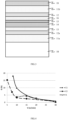
- the square resistance was measured before and after heat treatment.
- the square resistance (Rsq) was measured by a non-contact measurement by induction using an SRM-12 device marketed by Nagy.
- FIG.4 shows for each sample the squared resistance gain (G) of the stack after heat treatment as a function of the treatment speed (V).
- G squared resistance gain
- V treatment speed
- Table 3 summarizes the characteristics of the samples obtained for treatment speeds corresponding to the optimal conditions for each of the samples, that is to say conferring the best compromise between the gain of high square resistance and low residual absorption (light absorption after treatment thermal).
- the light absorption was measured according to the ISO 9050:2003 standard using a CM-3700d spectrophotometer marketed by Konika-Minolta.
- Table 3 Sample C1 C2 I1 Processing speed (m/min) 4 10 8 Forward Rsp ( ⁇ /sq) 4.33 3.78 3.69 Rsp after ( ⁇ /sq) 3.55 3.65 3.02 Gain (%) 18.0 3.44 18.2 Residual absorption (%) 6.54 11.1 7.26
Description
L'invention se rapporte au domaine des couches minces inorganiques, notamment déposées sur des substrats en verre. Elle concerne plus particulièrement un procédé d'obtention d'un matériau comprenant un substrat revêtu sur au moins une face d'un empilement de couches minces bas-émissif.The invention relates to the field of inorganic thin layers, in particular deposited on glass substrates. It relates more particularly to a process for obtaining a material comprising a substrate coated on at least one face with a stack of low-emissivity thin layers.
De nombreuses couches minces sont déposées sur des substrats, notamment en verre plat ou faiblement bombé, afin de conférer aux matériaux obtenus des propriétés particulières : propriétés optiques, par exemple de réflexion ou d'absorption de rayonnements d'un domaine de longueurs d'onde données, propriétés de conduction électrique particulière, ou encore propriétés liées à la facilité de nettoyage ou à la possibilité pour le matériau de s'auto-nettoyer.Many thin layers are deposited on substrates, in particular flat or slightly curved glass, in order to give the materials obtained specific properties: optical properties, for example of reflection or absorption of radiation of a range of wavelengths data, particular electrical conduction properties, or even properties related to the ease of cleaning or the possibility for the material to self-clean.
Un procédé couramment employé à l'échelle industrielle pour le dépôt de couches minces, notamment sur substrat verrier, est le procédé de pulvérisation cathodique assisté par champ magnétique, appelé procédé « magnétron ». Dans ce procédé, un plasma est créé sous un vide poussé au voisinage d'une cible comprenant les éléments chimiques à déposer. Les espèces actives du plasma, en bombardant la cible, arrachent lesdits éléments, qui se déposent sur le substrat en formant la couche mince désirée. Ce procédé est dit « réactif » lorsque la couche est constituée d'un matériau résultant d'une réaction chimique entre les éléments arrachés de la cible et le gaz contenu dans le plasma. L'avantage majeur de ce procédé réside dans la possibilité de déposer sur une même ligne un empilement très complexe de couches en faisant successivement défiler le substrat sous différentes cibles, ce généralement dans un seul et même dispositif.A process commonly used on an industrial scale for the deposition of thin layers, in particular on a glass substrate, is the cathode sputtering process assisted by magnetic field, called the “magnetron” process. In this method, a plasma is created under a high vacuum in the vicinity of a target comprising the chemical elements to be deposited. The active species of the plasma, by bombarding the target, tear off said elements, which are deposited on the substrate, forming the desired thin layer. This process is said to be “reactive” when the layer consists of a material resulting from a chemical reaction between the elements torn from the target and the gas contained in the plasma. The major advantage of this method lies in the possibility of depositing on the same line a very complex stack of layers by successively making the substrate pass under different targets, this generally in a single and same device.
Ces couches minces sont le plus souvent à base de composés inorganiques : oxydes, nitrures, ou encore métaux. Leur épaisseur varie généralement de quelques nanomètres à quelques centaines de nanomètres, d'où leur qualificatif de « minces ».These thin layers are most often based on inorganic compounds: oxides, nitrides, or even metals. Their thickness generally varies from a few nanometers to a few hundred nanometers, hence their qualifier “thin”.
Parmi les plus intéressantes figurent les couches minces à base d'argent métallique, lesquelles ont des propriétés de conduction électrique et de réflexion des rayonnements infrarouges, d'où leur utilisation dans des vitrages à contrôle solaire, notamment anti-solaires (visant à diminuer la quantité d'énergie solaire entrante) et/ou à faible émissivité (visant à diminuer la quantité d'énergie dissipée vers l'extérieur d'un bâtiment ou d'un véhicule).Among the most interesting are the thin layers based on metallic silver, which have properties of electrical conduction and reflection of infrared radiation, hence their use in solar control glazing, in particular solar protection (aimed at reducing the incoming solar energy) and/or low emissivity (aimed at reducing the amount of energy dissipated outside a building or vehicle).
Afin notamment d'éviter l'oxydation de l'argent et d'atténuer ses propriétés de réflexion dans le visible, la ou chaque couche d'argent est généralement insérée dans un empilement de couches. Dans le cas des vitrages à contrôle solaire ou à faible émissivité, la ou chaque couche mince à base d'argent est généralement disposée entre deux couches minces diélectriques à base d'oxyde ou de nitrure (par exemple en TiO2, SnO2 ou Si3N4). Peuvent être également disposées sous la couche d'argent une couche très fine destinée à favoriser le mouillage et la nucléation de l'argent (par exemple en oxyde de zinc ZnO) et sur la couche d'argent une seconde couche très fine (sacrificielle, par exemple en titane) destinée à protéger la couche d'argent au cas où le dépôt de la couche subséquente est réalisé dans une atmosphère oxydante ou en cas de traitements thermiques conduisant à une migration d'oxygène au sein de l'empilement. Ces couches sont respectivement appelées couche de mouillage et couche de bloqueur.
Les couches d'argent présentent la particularité de voir certaines de leurs propriétés améliorées lorsqu'elles sont dans un état au moins partiellement cristallisé. On cherche généralement à augmenter au maximum le taux de cristallisation de ces couches (la proportion massique ou volumique de matière cristallisée) et la taille des grains cristallins (ou la taille de domaines cohérents de diffraction mesurés par des méthodes de diffraction des rayons X). Il est notamment connu que les couches d'argent présentant un taux de cristallisation élevé et par conséquent une faible teneur résiduelle en grains nanométriques présentent une émissivité et une résistivité plus basses ainsi qu'une transmission dans le visible plus élevée que des couches d'argent majoritairement nano-cristallisées. La conductivité électrique et les propriétés de faible émissivité de ces couches sont ainsi améliorées. L'augmentation de la taille des grains s'accompagne en effet d'une diminution des joints de grains, favorable à la mobilité des porteurs de charge électrique.The silver layers have the particularity of seeing some of their properties improved when they are in an at least partially crystallized state. It is generally sought to increase as much as possible the rate of crystallization of these layers (the mass or volume proportion of crystallized material) and the size of the crystalline grains (or the size of coherent diffraction domains measured by X-ray diffraction methods). It is known in particular that silver layers having a high crystallization rate and consequently a low residual content of nanometric grains have lower emissivity and resistivity as well as higher transmission in the visible than silver layers. mostly nano-crystallized. The electrical conductivity and the low emissivity properties of these layers are thus improved. The increase in the size of the grains is in fact accompanied by a reduction in the grain boundaries, favorable to the mobility of the electric charge carriers.
Les couches d'argent déposées par procédé magnétron sont généralement majoritairement voire totalement nano-cristallisées (la taille moyenne des grains cristallins étant inférieure à quelques nanomètres), et des traitements thermiques se révèlent nécessaires pour obtenir le taux de cristallisation souhaité ou la taille de grains désirée.The silver layers deposited by the magnetron process are generally mostly or even completely nano-crystallized (the average size of the crystalline grains being less than a few nanometers), and heat treatments prove necessary to obtain the desired crystallization rate or the grain size. desired.
Il est connu d'effectuer un recuit laser local et rapide de revêtements comprenant une ou plusieurs couches d'argent. Pour cela on fait défiler le substrat avec le revêtement à recuire sous une ligne laser, ou bien une ligne laser au-dessus du substrat portant le revêtement. Le recuit laser permet de chauffer des revêtements minces à des températures élevées, de l'ordre de plusieurs centaines de degrés, tout en préservant le substrat sous-jacent. Les vitesses de défilement sont bien entendu de préférence les plus élevées possibles, avantageusement au moins de plusieurs mètres par minute. Le choix de la vitesse de défilement adéquate résulte d'un compromis entre productivité d'une part et efficacité du traitement d'autre part. En effet, plus la vitesse de défilement est faible, plus la quantité d'énergie absorbée par le revêtement est importante et meilleure sera la cristallisation de la ou des couches d'argent.It is known to carry out local and rapid laser annealing of coatings comprising one or more layers of silver. For this, the substrate with the coating to be annealed is passed under a laser line, or else a laser line above the substrate bearing the coating. Laser annealing makes it possible to heat thin coatings to high temperatures, on the order of several hundred degrees, while preserving the underlying substrate. Scrolling speeds are of course preferably the highest possible, advantageously at least several meters per minute. The choice of the appropriate scrolling speed results from a compromise between productivity on the one hand and processing efficiency on the other. Indeed, the lower the running speed, the greater the quantity of energy absorbed by the coating and the better the crystallization of the silver layer or layers will be.
Afin d'obtenir les vitesses de dépôt convenables, les couches minces diélectriques à base d'oxydes sont généralement déposée par procédé magnétron réactif à partir d'une cible métallique ou en oxyde sous-stoechiométrique dans un plasma contenant de l'oxygène. Les paramètres de procédé, sont alors généralement réglés de façon à obtenir l'oxyde souhaité en proportion stœchiométrique. Cependant, il n'est pas rare que, suite à une fluctuation de ces paramètres au cours du procédé de dépôt, la couche d'oxyde déposée puisse présenter une composition sous-stoechiométrique. Il a été observé que, dans ce cas, le gain de résistivité des couches d'argent après recuit laser n'était pas aussi bon qu'attendu. En effet, en deçà d'un certain seuil de vitesse de défilement, le gain de résistivité peut avoir tendance à diminuer avec la diminution de la vitesse de défilement alors que celui-ci devrait au contraire augmenter.In order to obtain the suitable deposition rates, the thin oxide-based dielectric layers are generally deposited by a reactive magnetron process from a metallic or substoichiometric oxide target in a plasma containing oxygen. The process parameters are then generally adjusted so as to obtain the desired oxide in a stoichiometric proportion. However, it is not rare that, following a fluctuation of these parameters during the deposition process, the deposited oxide layer may have a sub-stoichiometric composition. It was observed that, in this case, the resistivity gain of the silver layers after laser annealing was not as good as expected. Indeed, below a certain scrolling speed threshold, the gain in resistivity may tend to decrease with the decrease in the scrolling speed whereas the latter should on the contrary increase.
L'invention, qui est définie par les revendications annexées, a pour but de proposer un procédé permettant d'obvier les inconvénients mentionnés ci-dessus. A cet effet, l'invention a pour objet un procédé d'obtention d'un matériau comprenant un substrat choisi parmi une feuille de verre, de vitrocéramique, ou d'une matière organique polymérique, revêtu sur au moins une face d'un empilement de couches minces comprenant les étapes suivantes :
- on dépose sur au moins une face dudit substrat un empilement de couches minces comprenant une première couche diélectrique, une couche de mouillage, une couche d'argent et une deuxième couche diélectrique,
- on traite thermiquement la au moins une face revêtue à l'aide d'au moins un rayonnement laser émettant dans au moins une longueur d'onde comprise entre 100 et 2000 nm, de préférence de sorte que la résistance carrée de l'empilement est diminuée d'au moins 5% ;
- a stack of thin layers comprising a first dielectric layer, a wetting layer, a silver layer and a second dielectric layer is deposited on at least one face of said substrate,
- the at least one coated face is heat treated using at least one laser radiation emitting in at least one wavelength between 100 and 2000 nm, preferably so that the sheet resistance of the stack is reduced at least 5%;
Dans la présente demande, l'expression « au voisinage de » associé à la position d'une première couche (en particulier la couche donneuse d'oxygène) par rapport à une deuxième couche (en particulier la couche diélectrique à base d'oxyde) signifie que la première couche peut-être au-dessus ou au-dessous de la deuxième couche, celles-ci pouvant être au contact ou séparée entre elles par d'autres couches, notamment jusqu'à deux autres couches, de préférence au plus une autre couche. Les termes « au-dessous » et « au-dessus », associés à la position d'une première couche par rapport à une deuxième couche, signifient que la première couche est plus proche, respectivement plus éloignée, du substrat que la deuxième couche. Ces termes n'excluent cependant pas la présence d'autres couches entre lesdites première et deuxième couches. Au contraire, une première couche « en contact direct » avec une deuxième couche signifie qu'aucune autre couche n'est disposée entre celles-ci. Il en va de même pour les expressions « directement au-dessus » et « directement au-dessous ». Ainsi, il est entendu que, sauf s'il est indiqué autrement, d'autres couche peuvent être intercalées entre chacune des couches de l'empilement.In the present application, the expression "in the vicinity of" associated with the position of a first layer (in particular the oxygen donor layer) with respect to a second layer (in particular the dielectric layer based on oxide) means the first layer maybe above or below the second layer, these which may be in contact with or separated from each other by other layers, in particular up to two other layers, preferably at most one other layer. The terms “below” and “above”, associated with the position of a first layer with respect to a second layer, mean that the first layer is closer, respectively further away, from the substrate than the second layer. These terms do not however exclude the presence of other layers between said first and second layers. On the contrary, a first layer "in direct contact" with a second layer means that no other layer is placed between them. The same goes for the expressions “directly above” and “directly below”. Thus, it is understood that, unless indicated otherwise, other layers can be interposed between each of the layers of the stack.
Sans vouloir être lié à une quelconque théorie, il est en effet supposé que lorsque la couche diélectrique à base d'oxyde est sous-stœchiométrique en oxygène, celle-ci tend à réduire les couches environnantes en « pompant » l'oxygène des couches environnantes, notamment de la couche de mouillage, sous l'effet du recuit laser. Cela aurait pour effet d'altérer la couche de mouillage sur laquelle la couche d'argent se cristallise et de détériorer par conséquent la qualité de la couche d'argent. La présence d'une couche donneuse d'oxygène au voisinage de la couche diélectrique à base d'oxyde permet d'empêcher ce phénomène. L'oxygène pompé par la couche diélectrique à base d'oxyde proviendra en effet prioritairement de la couche donneuse en oxygène, ce qui a pour effet de protéger de protéger la couche de mouillage.Without wanting to be bound to any theory, it is indeed assumed that when the oxide-based dielectric layer is under-stoichiometric in oxygen, it tends to reduce the surrounding layers by "pumping" oxygen from the surrounding layers. , in particular of the wetting layer, under the effect of laser annealing. This would have the effect of altering the wetting layer on which the silver layer crystallizes and consequently deteriorating the quality of the silver layer. The presence of an oxygen-donating layer in the vicinity of the oxide-based dielectric layer makes it possible to prevent this phenomenon. The oxygen pumped by the oxide-based dielectric layer will indeed come primarily from the oxygen-donating layer, which has the effect of protecting and protecting the wetting layer.
Le substrat est une feuille de verre, de vitrocéramique, ou d'une matière organique polymérique. Il est de préférence transparent, incolore (il s'agit alors d'un verre clair ou extra-clair) ou coloré, par exemple en bleu, vert, gris ou bronze. Le verre est de préférence de type silico-sodo-calcique, mais il peut également être en verre de type borosilicate ou alumino-borosilicate. Les matières organiques polymériques préférées sont le polycarbonate ou le polyméthacrylate de méthyle ou encore le polyéthylènetérephtalate (PET). Le substrat présente avantageusement au moins une dimension supérieure ou égale à 1 m, voire 2 m et même 3 m. L'épaisseur du substrat varie généralement entre 0,5 mm et 19 mm, de préférence entre 0,7 et 9 mm, notamment entre 2 et 8 mm, voire entre 4 et 6 mm. Le substrat peut être plan ou bombé, voire flexible.The substrate is a sheet of glass, glass-ceramic, or a polymeric organic material. It is preferably transparent, colorless (it is then a clear or extra-clear glass) or colored, for example blue, green, gray or bronze. The glass is preferably of the silico-soda-lime type, but it can also be of borosilicate or alumino-borosilicate glass. The preferred polymeric organic materials are polycarbonate or polymethyl methacrylate or else polyethylene terephthalate (PET). The substrate advantageously has at least one dimension greater than or equal to 1 m, or even 2 m and even 3 m. The thickness of the substrate generally varies between 0.5 mm and 19 mm, preferably between 0.7 and 9 mm, in particular between 2 and 8 mm, or even between 4 and 6 mm. The substrate can be flat or curved, even flexible.
Le substrat de verre est de préférence du type flotté, c'est-à-dire susceptible d'avoir été obtenu par un procédé consistant à déverser le verre fondu sur un bain d'étain en fusion (bain « float »). Dans ce cas, la couche à traiter peut aussi bien être déposée sur la face « étain » que sur la face « atmosphère » du substrat. On entend par faces « atmosphère » et « étain », les faces du substrat ayant été respectivement en contact avec l'atmosphère régnant dans le bain float et en contact avec l'étain fondu. La face étain contient une faible quantité superficielle d'étain ayant diffusé dans la structure du verre. Le substrat de verre peut également être obtenu par laminage entre deux rouleaux, technique permettant en particulier d'imprimer des motifs à la surface du verre.The glass substrate is preferably of the float type, that is to say likely to have been obtained by a process consisting in pouring the molten glass onto a bath of molten tin (“float” bath). In this case, the layer to be treated can just as easily be deposited on the “tin” face as on the “atmosphere” face of the substrate. By “atmosphere” and “tin” faces is meant the faces of the substrate having been respectively in contact with the atmosphere prevailing in the float bath and in contact with the molten tin. The tin face contains a small surface quantity of tin having diffused into the structure of the glass. The glass substrate can also be obtained by rolling between two rollers, a technique which makes it possible in particular to print patterns on the surface of the glass.
On entend par verre clair un verre silico-sodo-calcique obtenu par flottage, non revêtu de couches, et présentant une transmission lumineuse de l'ordre de 90%, une réflexion lumineuse de l'ordre de 8% et une transmission énergétique de l'ordre de 83% pour une épaisseur de 4 mm. Les transmissions et réflexions lumineuses et énergétiques sont telles que définies par la norme NF EN 410. Des verres clairs typiques sont par exemple commercialisés sous la dénomination SGG Planilux par la société Saint-Gobain Glass France ou sous la dénomination Planibel Clair par la société AGC Flat Glass Europe. Ces substrats sont classiquement employés pour la fabrication de vitrages bas-émissifs.By clear glass is meant a silico-soda-lime glass obtained by floating, not coated with layers, and having a light transmission of the order of 90%, a light reflection of the order of 8% and an energy transmission of l order of 83% for a thickness of 4 mm. Light and energy transmissions and reflections are as defined by standard NF EN 410. Typical clear glasses are for example marketed under the name SGG Planilux by the company Saint-Gobain Glass France or under the name Planibel Clair by the company AGC Flat Glass Europe. These substrates are conventionally used for the manufacture of low-emissivity glazing.
Le procédé selon l'invention n'est bien évidemment pas limité aux dépôts réalisés sur un substrat de verre clair ou sur un substrat de 4 mm d'épaisseur. Le revêtement peut être déposé sur un substrat choisi parmi une feuille de verre, de vitrocéramique, et une matière organique polymérique, mais l'absorption de l'empilement telle que défini selon l'invention est considéré comme ayant été déposé sur un substrat de verre clair dont l'épaisseur est de 4 mm.The method according to the invention is obviously not limited to deposits made on a clear glass substrate or on a 4 mm thick substrate. The coating can be deposited on a substrate chosen from among a sheet of glass, glass-ceramic, and a polymeric organic material, but the absorption of the stack as defined according to the invention is considered to have been deposited on a glass substrate. clear whose thickness is 4 mm.
L'empilement de couches minces est déposé de préférence par pulvérisation cathodique. Il comprend successivement à partir du substrat une première couche diélectrique, une couche de mouillage, une couche d'argent et une deuxième couche diélectrique, au moins une desdites premières et deuxièmes couches diélectriques étant une couche diélectrique à base d'oxyde et une couche donneuse d'oxygène est disposée au voisinage de la couche diélectrique à base d'oxyde, de préférence en contact direct (directement au-dessus ou directement au-dessous) avec la couche diélectrique à base d'oxyde.The stack of thin layers is preferably deposited by sputtering. It comprises successively from the substrate a first dielectric layer, a wetting layer, a silver layer and a second dielectric layer, at least one of said first and second dielectric layers being an oxide-based dielectric layer and a donor layer oxygen is placed in the vicinity of the dielectric layer based on oxide, preferably in direct contact (directly above or directly below) with the dielectric layer based on oxide.
Par « couche donneuse d'oxygène » on entend une couche à base d'oxyde qui est susceptible de donner de l'oxygène à la couche diélectrique à base d'oxyde notamment lors du traitement thermique. La couche donneuse d'oxygène est à base d'un oxyde dont le potentiel redox est inférieur au matériau de la couche de mouillage, qui est de préférence l'oxyde de zinc. La couche donneuse d'oxygène sert de réservoir à oxygène à la couche diélectrique à base d'oxyde et protège ainsi la couche de mouillage en diminuant, voire en supprimant, la migration d'oxygène depuis la couche de mouillage vers la couche diélectrique à base d'oxyde lors du traitement thermique selon l'invention.By “oxygen-donating layer” is meant an oxide-based layer which is capable of donating oxygen to the oxide-based dielectric layer in particular during the heat treatment. The oxygen donor layer is based on an oxide whose redox potential is lower than the material of the wetting layer, which is preferably zinc oxide. The oxygen-donating layer serves as an oxygen reservoir for the oxide-based dielectric layer and thus protects the wetting layer by reducing, or even eliminating, the migration of oxygen from the wetting layer to the of oxide during the heat treatment according to the invention.
La couche donneuse d'oxygène est de préférence une couche à base d'oxyde mixte de d'étain et de zinc. Elle peut être par exemple une couche d'oxyde d'étain ou d'oxyde mixte d'étain et de zinc SnxZnyO avec une teneur atomique en étain de 0,3 ≤ x < 1,0 et x + y = 1 ; voire 0,5 ≤ x < 1,0 et x + y = 1. La couche donneuse d'oxygène peut être oxydée selon la stoechiométrie stable ou éventuellement sur-stœchiométrique en oxygène. La couche donneuse d'oxygène présente généralement une épaisseur de 1 à 30 nm, de préférence au moins 3, 4 voire 5 nm et au plus 20 nm, voir au plus 15 nm ou même 10 nm.The oxygen-donating layer is preferably a layer based on a mixed oxide of tin and zinc. It can be for example a layer of tin oxide or of mixed tin and zinc oxide Sn x Zn y O with an atomic tin content of 0.3 ≤ x < 1.0 and x + y = 1; or even 0.5≤x<1.0 and x+y=1. The oxygen donor layer can be oxidized according to the stable stoichiometry or possibly over-stoichiometric in oxygen. The oxygen donor layer generally has a thickness of 1 to 30 nm, preferably at least 3, 4 or even 5 nm and at most 20 nm, see at most 15 nm or even 10 nm.
Lorsque la première couche diélectrique est une couche diélectrique à base d'oxyde, la couche donneuse d'oxygène est disposée au-dessous de la couche de mouillage, de préférence en contact direct (directement au-dessus ou directement au-dessous) avec la première couche diélectrique à base d'oxyde. Lorsque la deuxième couche diélectrique est une couche diélectrique à base d'oxyde, la couche donneuse d'oxygène est disposée au-dessus de la couche d'argent, de préférence en contact direct (directement au-dessus ou directement au-dessous) avec la deuxième couche diélectrique à base d'oxyde.When the first dielectric layer is an oxide-based dielectric layer, the oxygen-donating layer is disposed below the wetting layer, preferably in direct contact (directly above or directly below) with the first dielectric layer based on oxide. When the second dielectric layer is an oxide-based dielectric layer, the oxygen-donating layer is disposed above the silver layer, preferably in direct contact (directly above or directly below) with the second oxide-based dielectric layer.
L'expression « couche diélectrique » au sens de la présente invention désigne une couche non métallique, c'est-à-dire qui n'est pas constituée de métal. Cette expression désigne notamment une couche constituée d'un matériau dont le rapport entre l'indice de réfraction et le coefficient d'extinction (n/k) sur toute la plage de longueur d'onde du visible (de 380 nm à 780 nm) est égal ou supérieur à 5.The expression “dielectric layer” within the meaning of the present invention designates a non-metallic layer, that is to say which is not made of metal. This expression designates in particular a layer made of a material whose ratio between the refractive index and the extinction coefficient (n/k) over the entire visible wavelength range (from 380 nm to 780 nm) is equal to or greater than 5.
La couche diélectrique à base d'oxyde est généralement sous-stoechiométrique, c'est-à-dire que la proportion d'oxygène est inférieure à celle la forme stable de l'oxyde considéré. Par exemple, pour un oxyde d'un métal divalent de formule stable MO, un oxyde sous-stoechiométrique peut être défini par la formule MOx avec x compris entre 0,6 et 0,99, de préférence entre 0,8 et 0,99 ; pour un oxyde d'un métal tétravalent de formule stable MO2, un oxyde sous-stoechiométrique peut être défini par la formule MOx avec x compris entre 1,5 et 1,99 ; de préférence entre 1,8 et 1,99 ; pour un oxyde de métal trivalent de formule stable M2O3, un oxyde sous-stœchiométrique peut être défini par la formule M2Ox avec x compris entre 2 et 2,99, de préférence entre 2,6 et 2,99 ; pour un oxyde de métal hexavalent de formule stable MO3, un oxyde sous-stoechiométrique peut être défini par la formule MOx avec x compris entre 2 et 2,99, de préférence entre 2,6 et 2,99. Elle peut être par exemple une couche à base d'oxyde de titane, de silicium, de niobium ou de magnésium. La couche diélectrique à base d'oxyde est de préférence une couche d'oxyde de titane, notamment une couche d'oxyde de titane sous-stœchiométrique TiOx (x étant alors strictement inférieur à 2). Selon un mode de réalisation particulier, la valeur de x est de préférence inférieure ou égale à 1,8, notamment entre 1,5 et 1,8. Dans ce cas, la couche diélectrique participe à l'absorption du rayonnement laser ce qui permet ainsi d'améliorer la cristallisation de la couche d'argent et/ou d'augmenter la vitesse de défilement lors du traitement thermique, et donc la productivité. Selon un autre mode de réalisation particulier, la première couche diélectrique est une couche d'oxyde de titane faiblement sous-stoechiométrique, c'est-à-dire que la valeur x est supérieure ou égale à 1,8, de préférence supérieure à 1,9. Il n'est pas rare en effet que les paramètres de procédé, bien que fixés initialement pour déposer une couche de TiO2 stoechiométrique (dans un souci notamment de réduire l'absorption résiduelle de l'empilement), puissent fluctuer au cours de la production de sorte que la couche effectivement déposée soit faiblement sous-stoechiométrique.The oxide-based dielectric layer is generally sub-stoichiometric, ie the proportion of oxygen is lower than that of the stable form of the oxide considered. For example, for an oxide of a divalent metal with the stable formula MO, a sub-stoichiometric oxide can be defined by the formula MO x with x between 0.6 and 0.99, preferably between 0.8 and 0.99; for an oxide of a tetravalent metal of stable formula MO 2 , a sub-stoichiometric oxide can be defined by the formula MO x with x between 1.5 and 1.99; preferably between 1.8 and 1.99; for a trivalent metal oxide of stable formula M 2 O 3 , a sub-stoichiometric oxide can be defined by the formula M 2 O x with x between 2 and 2.99, preferably between 2.6 and 2.99; for a hexavalent metal oxide of stable formula MO 3 , a sub-stoichiometric oxide can be defined by the formula MO x with x between 2 and 2.99, preferably between 2.6 and 2.99. It may for example be a layer based on titanium, silicon, niobium or magnesium oxide. The oxide-based dielectric layer is preferably a layer of titanium oxide, in particular a layer of sub-stoichiometric titanium oxide TiO x (x then being strictly less than 2). According to a particular embodiment, the value of x is preferably less than or equal to 1.8, in particular between 1.5 and 1.8. In this case, the dielectric layer takes part in the absorption of the laser radiation, which thus makes it possible to improve the crystallization of the silver layer and/or to increase the running speed during the heat treatment, and therefore the productivity. According to another particular embodiment, the first dielectric layer is a layer of slightly sub-stoichiometric titanium oxide, that is to say that the value x is greater than or equal to 1.8, preferably greater than 1 ,9. It is not rare indeed that the process parameters, although initially fixed to deposit a layer of stoichiometric TiO 2 (for the sake in particular of reducing the residual absorption of the stack), can fluctuate during the production so that the layer actually deposited is slightly sub-stoichiometric.
L'autre couche diélectrique (celle de la première ou deuxième couche diélectrique qui n'est pas nécessairement à base d'oxyde) peut être à base d'oxyde, éventuellement sous-stoechiométrique, notamment en oxyde de titane, en oxyde d'étain, en oxyde de silicium ou leurs mélanges, ou de nitrure, notamment en nitrure de silicium.The other dielectric layer (that of the first or second dielectric layer which is not necessarily oxide-based) can be oxide-based, optionally sub-stoichiometric, in particular titanium oxide, tin oxide, silicon oxide or mixtures thereof, or nitride, in particular silicon nitride.
Dans un mode de réalisation particulier, chacune des première et deuxième couches diélectriques est une couche à base d'oxyde, en particulier une couche à base d'oxyde de titane, notamment une couche d'oxyde de titane sous-stoechiométrique TiOx telle que définie ci-dessus. Dans ce cas, l'empilement selon l'invention peut comprendre deux couches donneuses d'oxygène, respectivement au voisinage de chacune des première et deuxième couches diélectriques. Selon ce mode de réalisation, l'empilement peut comprendre successivement à partir du substrat une première couche diélectrique à base d'oxyde, une première couche donneuse d'oxygène, une couche de mouillage à base d'oxyde de zinc, une couche d'argent, une deuxième couche donneuse d'oxygène et une deuxième couche diélectrique à base d'oxyde ; alternativement, la première couche donneuse d'oxygène peut être disposée entre le substrat et la première couche diélectrique à base d'oxyde, et/ou la deuxième couche donneuse d'oxygène peut être disposée au-dessus de la deuxième couche diélectrique à base d'oxyde.In a particular embodiment, each of the first and second dielectric layers is a layer based on oxide, in particular a layer based on titanium oxide, in particular a layer of sub-stoichiometric titanium oxide TiO x such that defined above. In this case, the stack according to the invention can comprise two oxygen donor layers, respectively in the vicinity of each of the first and second dielectric layers. According to this embodiment, the stack may successively comprise, starting from the substrate, a first dielectric layer based on oxide, a first oxygen-donating layer, a wetting layer based on zinc oxide, a layer of silver, a second oxygen-donating layer and a second oxide-based dielectric layer; alternatively, the first oxygen-donating layer may be disposed between the substrate and the first oxide-based dielectric layer, and/or the second oxygen-donating layer may be disposed above the second oxide-based dielectric layer 'oxide.
Les première et deuxième couches diélectriques ont généralement chacune une épaisseur de 10 à 60 nm, de préférence 15 à 50 nm.The first and second dielectric layers generally each have a thickness of 10 to 60 nm, preferably 15 to 50 nm.
L'empilement selon l'invention peut comprendre une couche de sur-bloqueur et/ou de de sous-bloqueur respectivement au-dessus ou au-dessous de la ou chaque couche d'argent et en contact direct avec celle-ci. Les couches de bloqueur (sous-bloqueur et/ou sur-bloqueur) sont généralement à base d'un métal choisi parmi le nickel, le chrome, le titane, le niobium, ou d'un alliage de ces différents métaux. On peut notamment citer les alliages nickel-titane (notamment ceux comprenant environ 50% en poids de chaque métal) ou les alliages nickel-chrome (notamment ceux comprenant 80% en poids de nickel et 20% en poids de chrome). La couche de sur-bloqueur peut encore être constituée de plusieurs couches superposées, par exemple, en s'éloignant du substrat, de titane puis d'un alliage de nickel (notamment un alliage nickel-chrome) ou l'inverse. Ces couches de bloqueur (sous-bloqueur et/ou sur-bloqueur) sont très fines, normalement d'une épaisseur inférieure à 1 nm, pour ne pas affecter la transmission lumineuse de l'empilement, et sont susceptibles d'être partiellement oxydées pendant le traitement thermique selon l'invention. D'une manière générale les couches de bloqueur sont des couches sacrificielles, susceptibles de capter l'oxygène provenant de l'atmosphère ou du substrat, évitant ainsi l'oxydation de la couche d'argent.The stack according to the invention may comprise a layer of over-blocker and/or of under-blocker respectively above or below the or each layer of silver and in direct contact with the latter. The blocker layers (under-blocker and/or over-blocker) are generally based on a metal chosen from nickel, chromium, titanium, niobium, or on an alloy of these different metals. Mention may in particular be made of nickel-titanium alloys (in particular those comprising approximately 50% by weight of each metal) or nickel-chromium alloys (in particular those comprising 80% by weight of nickel and 20% by weight of chromium). The overblocker layer may also consist of several superimposed layers, for example, moving away from the substrate, of titanium then of a nickel alloy (in particular a nickel-chromium alloy) or the reverse. These layers of blocker (under-blocker and/or over-blocker) are very thin, normally less than 1 nm thick, so as not to affect the light transmission of the stack, and are likely to be partially oxidized during the heat treatment according to the invention. In general, the blocker layers are sacrificial layers, capable of capturing oxygen coming from the atmosphere or from the substrate, thus avoiding oxidation of the silver layer.
La couche de mouillage est généralement à base d'oxyde de zinc. Elle est de préférence constituée d'oxyde de zinc, éventuellement dopée à l'aluminium. La couche de mouillage est généralement disposée au-dessous de la couche d'argent et en contact direct avec celle-ci ou, lorsqu'une couche de bloqueur est présente, en contact direct avec la couche de bloqueur. Elle a généralement une épaisseur de 2 à 10 nm, de préférence de 3 à 8 nm.The wetting layer is generally based on zinc oxide. It preferably consists of zinc oxide, optionally doped with aluminum. The wetting layer is generally disposed below the silver layer and in direct contact with the latter or, when a blocker layer is present, in direct contact with the blocker layer. It generally has a thickness of 2 to 10 nm, preferably 3 to 8 nm.
L'empilement peut comprendre une ou plusieurs couches d'argent, notamment deux ou trois couches d'argent. Lorsque plusieurs couches d'argent sont présentes, l'architecture générale présentée ci-avant peut être répétée. Dans ce cas, la deuxième couche diélectrique relative à une couche d'argent donnée (donc situé au-dessus de cette couche d'argent) coïncide généralement avec la première couche diélectrique relative à la couche d'argent suivante. De préférence, l'épaisseur physique de la ou chaque couche d'argent est comprise entre 6 et 20 nm.The stack may comprise one or more layers of silver, in particular two or three layers of silver. When several layers of silver are present, the general architecture presented above can be repeated. In this case, the second dielectric layer relating to a given silver layer (therefore situated above this silver layer) generally coincides with the first dielectric layer relating to the following silver layer. Preferably, the physical thickness of the or each layer of silver is between 6 and 20 nm.
L'empilement peut comprendre d'autres couches, notamment entre le substrat et la première couche diélectrique, directement au-dessus de la couche d'argent (ou de sur-bloqueur), ou encore au-dessus de la deuxième couche diélectrique.The stack can comprise other layers, in particular between the substrate and the first dielectric layer, directly above the silver layer (or over-blocker), or even above the second dielectric layer.
Une couche d'adhésion peut notamment être disposée directement au-dessus de la couche d'argent, ou si présente directement au-dessus de la couche de sur-bloqueur, afin d'améliorer l'adhésion entre la couche d'argent ou de sur-bloqueur et les couches supérieures. La couche d'adhésion peut être par exemple une couche d'oxyde de zinc, notamment dopé à l'aluminium, ou encore une couche d'oxyde d'étain. Elle a généralement une épaisseur de 2 à 10 nm.An adhesion layer may in particular be placed directly above the silver layer, or if present directly above the overblocker layer, in order to improve the adhesion between the silver layer or over-blocker and top layers. The adhesion layer may for example be a layer of zinc oxide, in particular doped with aluminum, or else a layer of tin oxide. It is generally 2 to 10 nm thick.
La première couche diélectrique est de préférence déposée directement au-dessus du substrat. Pour adapter au mieux les propriétés optiques de l'empilement (notamment l'aspect en réflexion), une sous-couche peut alternativement être disposée entre la première couche diélectrique et le substrat, de préférence en contact direct avec ceux-ci. Cette sous-couche peut être une couche à base d'oxyde ou de nitrure, notamment de nitrure de silicium éventuellement dopé à l'aluminium. Elle a généralement une épaisseur de 2 à 30 mm, de préférence 3 à 20 nm, voire 5 à 15 nm.The first dielectric layer is preferably deposited directly above the substrate. To best adapt the optical properties of the stack (in particular the appearance in reflection), an under-layer can alternatively be placed between the first dielectric layer and the substrate, preferably in direct contact with the latter. This sub-layer can be a layer based on oxide or nitride, in particular silicon nitride optionally doped with aluminum. It generally has a thickness of 2 to 30 mm, preferably 3 to 20 nm, or even 5 to 15 nm.
Une couche de protection peut être disposée sur la deuxième couche diélectrique. Cette couche de protection constitue généralement la dernière couche de l'empilement et est destinée notamment à protéger l'empilement contre toutes agressions mécaniques (rayures...) ou chimiques. Elle peut être une couche à base d'oxyde ou de nitrure, notamment de nitrure de silicium. La couche de protection a généralement une épaisseur de 3 à 50 nm.A protective layer may be placed on the second dielectric layer. This protective layer generally constitutes the last layer of the stack and is intended in particular to protect the stack against any mechanical (scratches, etc.) or chemical attacks. It may be a layer based on an oxide or a nitride, in particular silicon nitride. The protective layer generally has a thickness of 3 to 50 nm.
Les
Des exemples d'empilement selon l'invention peuvent être choisis parmi :
- Substrat//TiOx/SnZnO/ZnO/Ag/Ti/ZnO/TiO2/Si3N4
- Substrat//SnZnO/TiOx/ZnO/Ag/Ti/ZnO/TiO2/Si3N4
- Substrat//TiOx/SnZnO/ZnO/Ti/Ag/Ti/ZnO/TiO2/Si3N4
- Substrat//SnZnO/TiOx/ZnO/Ti/Ag/Ti/ZnO/TiO2/Si3N4
- Substrat//TiO2/ZnO/Ag/Ti/ZnO/SnZnO/TiOx/Si3N4
- Substrat//TiO2/ZnO/Ag/Ti/ZnO/TiOx/SnZnO/Si3N4
- Substrat//TiO2/ZnO/Ti/Ag/Ti/ZnO/SnZnO/TiOx/Si3N4
- Substrat//TiO2/ZnO/Ti/Ag/Ti/ZnO/TiOx/SnZnO/Si3N4
- Substrat//TiOx/SnZnO/ZnO/Ag/Ti/ZnO/SnZnO/TiOx/Si3N4
- Substrat//SnZnO/TiOx/ZnO/Ag/Ti/ZnO/SnZnO/TiOx/Si3N4
- Substrat//TiOx/SnZnO/ZnO/Ag/Ti/ZnO/TiOx/SnZnO/Si3N4
- Substrat//SnZnO/TiOx/ZnO/Ag/Ti/ZnO/TiOx/SnZnO/Si3N4
- Substrat//TiOx/SnZnO/ZnO/Ti/Ag/Ti/ZnO/SnZnO/TiOx/Si3N4
- Substrat//SnZnO/TiOx/ZnO/Ti/Ag/Ti/ZnO/SnZnO/TiOx/Si3N4
- Substrat//TiOx/SnZnO/ZnO/Ti/Ag/Ti/ZnO/TiOx/SnZnO/Si3N4
- Substrat//SnZnO/TiOx/ZnO/Ti/Ag/Ti/ZnO/TiOx/SnZnO/Si3N4
- Substrate//TiO x /SnZnO/ZnO/Ag/Ti/ZnO/TiO 2 /Si 3 N 4
- Substrate//SnZnO/TiO x /ZnO/Ag/Ti/ZnO/TiO 2 /Si 3 N 4
- Substrate//TiO x /SnZnO/ZnO/Ti/Ag/Ti/ZnO/TiO 2 /Si 3 N 4
- Substrate//SnZnO/TiO x /ZnO/Ti/Ag/Ti/ZnO/TiO 2 /Si 3 N 4
- Substrate//TiO 2 /ZnO/Ag/Ti/ZnO/SnZnO/TiO x /Si 3 N 4
- Substrate//TiO 2 /ZnO/Ag/Ti/ZnO/TiO x /SnZnO/Si 3 N 4
- Substrate//TiO 2 /ZnO/Ti/Ag/Ti/ZnO/SnZnO/TiO x /Si 3 N 4
- Substrate//TiO 2 /ZnO/Ti/Ag/Ti/ZnO/TiO x /SnZnO/Si 3 N 4
- Substrate//TiO x /SnZnO/ZnO/Ag/Ti/ZnO/SnZnO/TiO x /Si 3 N 4
- Substrate//SnZnO/TiO x /ZnO/Ag/Ti/ZnO/SnZnO/TiO x /Si 3 N 4
- Substrate//TiO x /SnZnO/ZnO/Ag/Ti/ZnO/TiO x /SnZnO/Si 3 N 4
- Substrate//SnZnO/TiO x /ZnO/Ag/Ti/ZnO/TiO x /SnZnO/Si 3 N 4
- Substrate//TiO x /SnZnO/ZnO/Ti/Ag/Ti/ZnO/SnZnO/TiO x /Si 3 N 4
- Substrate//SnZnO/TiO x /ZnO/Ti/Ag/Ti/ZnO/SnZnO/TiO x /Si 3 N 4
- Substrate//TiO x /SnZnO/ZnO/Ti/Ag/Ti/ZnO/TiO x /SnZnO/Si 3 N 4
- Substrate//SnZnO/TiO x /ZnO/Ti/Ag/Ti/ZnO/TiO x /SnZnO/Si 3 N 4
Le procédé selon l'invention comprend également une étape de traitement thermique à l'aide d'un laser. Ce traitement thermique permet d'apporter une énergie suffisante pour favoriser la cristallisation de la couche mince d'argent, par un mécanisme physico-chimique de croissance cristalline autour de germes déjà présents dans la couche, en restant en phase solide. Le fait de favoriser la cristallisation de la couche d'argent peut notamment se traduire en une disparition des éventuels résidus de phase amorphe et/ou en une augmentation de la taille des domaines cohérents de diffraction et/ou en une diminution de la densité de défauts ponctuels (lacunes, interstitiels) ou de défauts surfaciques ou volumiques tels que les macles.The method according to the invention also comprises a step of heat treatment using a laser. This heat treatment makes it possible to provide sufficient energy to promote the crystallization of the thin layer of silver, by a physico-chemical mechanism of crystal growth around seeds already present in the layer, while remaining in the solid phase. Promoting the crystallization of the silver layer can in particular result in a disappearance of any amorphous phase residues and/or in an increase in the size of the coherent diffraction domains and/or in a decrease in the density of point defects (vacancies, interstitials) or surface or volume defects such as than twins.
Le procédé selon l'invention présente l'avantage de ne chauffer que l'empilement bas-émissif, sans échauffement significatif de la totalité du substrat. Il n'est ainsi plus nécessaire de procéder à un refroidissement lent et contrôlé du substrat avant la découpe ou le stockage du verre.The method according to the invention has the advantage of heating only the low-emissivity stack, without significant heating of the entire substrate. It is thus no longer necessary to carry out a slow and controlled cooling of the substrate before cutting or storing the glass.
L'utilisation d'un rayonnement laser présente l'avantage d'obtenir des températures généralement inférieures à 100°C, et même souvent inférieures à 50°C au niveau de la face opposée à la première face du substrat (c'est-à-dire au niveau de la face non revêtue). Cette caractéristique particulièrement avantageuse est due au fait que le coefficient d'échange thermique est très élevé, typiquement supérieur à 400 W/(m2.s). La puissance surfacique du rayonnement laser au niveau de l'empilement à traiter est même de préférence supérieure ou égale à 10, voire 20 ou 30 kW/cm2.The use of laser radiation has the advantage of obtaining temperatures generally lower than 100°C, and often even lower than 50°C at the level of the face opposite the first face of the substrate (i.e. say at the level of the uncoated face). This particularly advantageous characteristic is due to the fact that the heat exchange coefficient is very high, typically greater than 400 W/(m 2 .s). The surface power of the laser radiation at the level of the stack to be treated is even preferably greater than or equal to 10, or even 20 or 30 kW/cm 2 .
Cette très forte densité d'énergie permet d'atteindre au niveau de l'empilement la température souhaitée extrêmement rapidement (en général en un temps inférieur ou égal à 1 seconde) et par conséquent de limiter d'autant la durée du traitement, la chaleur générée n'ayant alors pas le temps de diffuser au sein du substrat. Ainsi, chaque point de l'empilement est de préférence soumis au traitement selon l'invention (et notamment porté à une température supérieure ou égale à 300°C) pour une durée généralement inférieure ou égale à 1 seconde, voire 0,5 seconde.This very high energy density makes it possible to reach the desired temperature extremely quickly at the level of the stack (generally in a time less than or equal to 1 second) and consequently to limit the duration of the treatment, the heat generated then not having time to diffuse within the substrate. Thus, each point of the stack is preferably subjected to the treatment according to the invention (and in particular brought to a temperature greater than or equal to 300° C.) for a duration generally less than or equal to 1 second, or even 0.5 second.
Grâce au très fort coefficient d'échange thermique associé au procédé selon l'invention, la partie du verre située à 0,5 mm de la couche mince ne subit généralement pas de températures supérieures à 100°C. La température de la face du substrat opposée à la face traitée par le au moins un rayonnement laser n'excède de préférence pas 100°C, notamment 50°C et même 30°C pendant le traitement thermique.Thanks to the very high coefficient of heat exchange associated with the process according to the invention, the part of the glass situated at 0.5 mm from the thin layer does not generally undergo temperatures above 100° C. The temperature of the face of the substrate opposite the face treated with the at least one laser radiation preferably does not exceed 100° C., in particular 50° C. and even 30° C. during the heat treatment.
L'essentiel de l'énergie apportée est donc « utilisée » par l'empilement afin d'améliorer les caractéristiques de cristallisation de la ou de chaque couche d'argent qu'il contient.Most of the energy supplied is therefore “used” by the stack in order to improve the crystallization characteristics of the or each layer of silver that it contains.
Ce procédé rend également possible l'intégration d'un dispositif de traitement laser sur les lignes de production continue existantes. Le laser peut être ainsi intégré dans une ligne de dépôt de couches, par exemple une ligne de dépôt par pulvérisation cathodique assistée par champ magnétique (procédé magnétron). La ligne comprend en général des dispositifs de manutention des substrats, une installation de dépôt, des dispositifs de contrôle optique, des dispositifs d'empilage. Les substrats défilent, par exemple sur des rouleaux convoyeurs, successivement devant chaque dispositif ou chaque installation. Le laser est de préférence situé juste après l'installation de dépôt de couches, par exemple à la sortie de l'installation de dépôt. Le substrat revêtu peut ainsi être traité en ligne après le dépôt de couches, à la sortie de l'installation de dépôt et avant les dispositifs de contrôle optique, ou après les dispositifs de contrôle optique et avant les dispositifs d'empilage des substrats. Il est également possible dans certains cas de réaliser le traitement thermique selon l'invention au sein même de l'enceinte de dépôt sous vide. Le laser est alors intégré à l'installation de dépôt. Par exemple, le laser peut être introduit dans une des chambres d'une installation de dépôt par pulvérisation cathodique.This process also makes it possible to integrate a laser processing device into existing continuous production lines. The laser can thus be integrated into a layer deposition line, for example a magnetic field-assisted sputtering deposition line (magnetron process). The line generally includes substrate handling devices, a deposition installation, optical control devices, stacking devices. The substrates pass, for example on conveyor rollers, successively in front of each device or each installation. The laser is preferably located just after the layer deposition installation, for example at the outlet of the deposition installation. The coated substrate can thus be treated in line after the deposition of layers, at the exit from the deposition installation and before the optical control devices, or after the optical control devices and before the substrate stacking devices. It is also possible in certain cases to carry out the heat treatment according to the invention within the vacuum deposition chamber itself. The laser is then integrated into the deposition installation. For example, the laser can be introduced into one of the chambers of a sputtering deposition installation.
Que le laser soit en dehors de ou intégré à l'installation de dépôt, ces procédés, dits en ligne ou en continu, sont préférables à un procédé en reprise dans lequel il serait nécessaire d'empiler les substrats de verre entre l'étape de dépôt et le traitement thermique.Whether the laser is outside or integrated into the deposition installation, these processes, called online or continuous, are preferable to a recovery process in which it would be necessary to stack the glass substrates between the step of deposition and heat treatment.
Les procédés en reprise peuvent toutefois avoir un intérêt dans les cas où la mise en oeuvre du traitement thermique selon l'invention est faite dans un lieu différent de celui où est réalisé le dépôt, par exemple dans un lieu où est réalisée la transformation du verre. Le dispositif de rayonnement peut donc être intégré à d'autres lignes que la ligne de dépôt de couches. Il peut par exemple être intégré à une ligne de fabrication de vitrages multiples (doubles ou triples vitrages notamment), ou à une ligne de fabrication de vitrages feuilletés. Dans ces différents cas, le traitement thermique selon l'invention est de préférence réalisé avant la réalisation du vitrage multiple ou feuilleté.The recovery processes may however have an interest in cases where the implementation of the heat treatment according to the invention is carried out in a place different from that where the deposition is carried out, for example in a place where the transformation of the glass is carried out. . The radiation device can therefore be integrated into lines other than the layer deposition line. It can for example be integrated into a production line for multiple glazing (double or triple glazing in particular), or into a production line for laminated glazing. In these various cases, the heat treatment according to the invention is preferably carried out before the production of the multiple or laminated glazing.
Le rayonnement laser est de préférence issu d'au moins un faisceau laser formant une ligne (appelée « ligne laser » dans la suite du texte) qui irradie simultanément toute la largeur du substrat. Le faisceau laser en ligne peut notamment être obtenu à l'aide de systèmes optiques de focalisation. Afin de pouvoir irradier simultanément des substrats de grande largeur (>3m), la ligne laser est généralement obtenue en combinant plusieurs lignes laser élémentaires. L'épaisseur des lignes laser élémentaires est de préférence comprise entre 0,01 et 1 mm. Leur longueur est typiquement comprise entre 5 mm et 1 m. Les lignes laser élémentaires sont généralement juxtaposées côte à côte pour former une ligne laser unique de sorte que toute la surface de l'empilement soit traitée. Chaque ligne laser élémentaire est de préférence disposée perpendiculairement à la direction de défilement du substrat.The laser radiation preferably comes from at least one laser beam forming a line (called “laser line” in the remainder of the text) which simultaneously irradiates the entire width of the substrate. The line laser beam can in particular be obtained using optical focusing systems. In order to be able to simultaneously irradiate large width substrates (>3m), the laser line is generally obtained by combining several elementary laser lines. The thickness of the elementary laser lines is preferably between 0.01 and 1 mm. Their length is typically between 5 mm and 1 m. The elementary laser lines are generally juxtaposed side by side to form a single laser line so that the entire surface of the stack is treated. Each elementary laser line is preferably arranged perpendicular to the running direction of the substrate.
Les sources laser sont typiquement des diodes laser ou des lasers fibrés, notamment des lasers à fibre, à diodes ou encore à disque. Les diodes laser permettent d'atteindre de manière économique de fortes densités de puissance par rapport à la puissance électrique d'alimentation, pour un faible encombrement. L'encombrement des lasers fibrés est encore plus réduit, et la puissance linéique obtenue peut être encore plus élevée, pour un coût toutefois plus important. On entend par lasers fibrés des lasers dans lesquels le lieu de génération du rayonnement laser est déporté spatialement par rapport à son lieu de délivrance, le rayonnement laser étant délivré au moyen d'au moins une fibre optique. Dans le cas d'un laser à disque, le rayonnement laser est généré dans une cavité résonnante dans laquelle se trouve le milieu émetteur qui se présente sous la forme d'un disque, par exemple un disque mince (d'environ 0,1 mm d'épaisseur) en Yb:YAG. Le rayonnement ainsi généré est couplé dans au moins une fibre optique dirigée vers le lieu de traitement. Le laser peut également être à fibre, au sens où le milieu d'amplification est lui-même une fibre optique. Les lasers à fibre ou à disque sont de préférence pompés optiquement à l'aide de diodes laser. Le rayonnement issu des sources laser est de préférence continu.The laser sources are typically laser diodes or fiber lasers, in particular fiber, diode or disc lasers. Laser diodes make it possible to economically achieve high power densities with respect to the electric power supply, for a small footprint. The bulk of fiber lasers is even more reduced, and the linear power obtained can be even higher, for a higher cost however. By fiber lasers is meant lasers in which the place of generation of the laser radiation is spatially offset with respect to its place of delivery, the laser radiation being delivered by means of at least one optical fiber. In the case of a disc laser, the laser radiation is generated in a resonant cavity in which the emitting medium is located, which is in the form of a disc, for example a thin disc (about 0.1 mm thick) in Yb:YAG. The radiation thus generated is coupled into at least one optical fiber directed towards the place of treatment. The laser can also be fiber, in the sense that the amplification medium is itself an optical fiber. Fiber or disc lasers are preferably optically pumped using laser diodes. The radiation from the laser sources is preferably continuous.
La longueur d'onde du rayonnement laser, donc la longueur d'onde de traitement, est de préférence comprise dans un domaine allant de 500 à 1300 nm, notamment de 800 à 1100 nm. Des diodes laser de puissance émettant à une ou plusieurs longueurs d'onde choisie parmi 808 nm, 880 nm, 915 nm, 940 nm ou 980 nm se sont révélées particulièrement bien appropriées. Dans le cas d'un laser à disque, la longueur d'onde de traitement est par exemple de 1030 nm (longueur d'onde d'émission pour un laser Yb :YAG). Pour un laser à fibre, la longueur d'onde de traitement est typiquement de 1070 nm.The wavelength of the laser radiation, therefore the treatment wavelength, is preferably within a range ranging from 500 to 1300 nm, in particular from 800 to 1100 nm. Power laser diodes emitting at one or more wavelengths chosen from 808 nm, 880 nm, 915 nm, 940 nm or 980 nm have proved to be particularly well suited. In the case of a disk laser, the treatment wavelength is for example 1030 nm (emission wavelength for a Yb:YAG laser). For a fiber laser, the treatment wavelength is typically 1070 nm.
De préférence, l'absorption de l'empilement à la longueur d'onde du rayonnement laser est supérieure ou égale à 5%, de préférence supérieure à 10 % ou 15%, voire supérieure à 20% ou même 30%. L'absorption est définie comme étant égale à la valeur de 100% auxquelles sont soustraites la transmission et la réflexion de la couche.Preferably, the absorption of the stack at the wavelength of the laser radiation is greater than or equal to 5%, preferably greater than 10% or 15%, or even greater than 20% or even 30%. The absorption is defined as being equal to the value of 100% from which the transmission and the reflection of the layer are subtracted.
Afin de traiter toute la surface du substrat revêtu, on crée un déplacement relatif entre d'une part le substrat revêtu de la couche et la ligne laser. Le substrat peut ainsi être mis en déplacement, notamment en défilement en translation en regard de la ligne laser fixe, généralement en dessous, mais éventuellement au-dessus de la ligne laser. Ce mode de réalisation est particulièrement appréciable pour un traitement en continu. De préférence, la vitesse de défilement, c'est-à-dire la différence entre les vitesses respectives du substrat et du laser, est supérieure ou égale à 1 m/min, voire supérieure à 2, 3, 4 ou 5 m/min, ou même avantageusement supérieure ou égale à 8 ou 10 m/min, ce afin d'assurer une grande vitesse de traitement.In order to treat the entire surface of the coated substrate, a relative displacement is created between, on the one hand, the substrate coated with the layer and the laser line. The substrate can thus be moved, in particular by scrolling in translation opposite the fixed laser line, generally below, but optionally above the laser line. This embodiment is particularly valuable for continuous processing. Preferably, the running speed, that is to say the difference between the respective speeds of the substrate and of the laser, is greater than or equal to 1 m/min, or even greater than 2, 3, 4 or 5 m/min , or even advantageously greater than or equal to 8 or 10 m/min, in order to ensure a high processing speed.
Le substrat peut être mis en mouvement à l'aide de tous moyens mécaniques de convoyage, par exemple à l'aide de bandes, de rouleaux, de plateaux en translation. Le système de convoyage permet de contrôler et réguler la vitesse du déplacement. Si le substrat est en matière organique polymérique souple, le déplacement peut être réalisé à l'aide d'un système d'avance de films sous forme d'une succession de rouleaux.The substrate can be set in motion using any mechanical conveying means, for example using strips, rollers, translation plates. The conveying system makes it possible to control and regulate the speed of movement. If the substrate is made of flexible polymeric organic material, the movement can be carried out using a film advance system in the form of a succession of rollers.
Toutes les positions relatives du substrat et du laser sont bien entendu possibles, du moment que la surface du substrat peut être convenablement irradiée. Le substrat sera le plus généralement disposé de manière horizontale, mais il peut aussi être disposé verticalement, ou selon toute inclinaison possible. Lorsque le substrat est disposé horizontalement, le laser est généralement disposé de manière à irradier la face supérieure du substrat. Le laser peut également irradier la face inférieure du substrat. Dans ce cas, il faut que le système de support du substrat, éventuellement le système de convoyage du substrat lorsque ce dernier est en mouvement, laisse passer le rayonnement dans la zone à irradier. C'est le cas par exemple lorsque l'on utilise des rouleaux de convoyage : les rouleaux étant disjoints, il est possible de disposer le laser dans une zone située entre deux rouleaux successifs.All relative positions of the substrate and of the laser are of course possible, as long as the surface of the substrate can be suitably irradiated. The substrate will most generally be arranged horizontally, but it can also be arranged vertically, or at any possible inclination. When the substrate is arranged horizontally, the laser is generally arranged so as to irradiate the upper face of the substrate. The laser can also irradiate the underside of the substrate. In this case, he the substrate support system, possibly the substrate conveying system when the latter is in motion, must allow the radiation to pass into the zone to be irradiated. This is the case, for example, when conveying rollers are used: the rollers being separate, it is possible to place the laser in a zone situated between two successive rollers.
La présente invention concerne également un matériau comprenant un substrat revêtu d'un revêtement bas-émissif tel que décrit ci-dessus. Le matériau selon l'invention est susceptible d'être obtenu par le procédé selon l'invention. Le matériau selon l'invention est de préférence incorporé à un vitrage. La présente invention concerne donc également un vitrage comprenant un matériau comprenant un substrat revêtu d'un revêtement bas émissif tel que décrit ci-dessus. Le vitrage peut être simple ou multiple (notamment double ou triple), au sens où il peut comprendre plusieurs feuilles de verre ménageant un espace rempli de gaz. Le vitrage peut également être feuilleté et/ou trempé et/ou durci et/ou bombé.The present invention also relates to a material comprising a substrate coated with a low-emissivity coating as described above. The material according to the invention is capable of being obtained by the method according to the invention. The material according to the invention is preferably incorporated into a glazing. The present invention therefore also relates to a glazing comprising a material comprising a substrate coated with a low-emissivity coating as described above. The glazing may be single or multiple (in particular double or triple), in the sense that it may comprise several sheets of glass providing a space filled with gas. The glazing may also be laminated and/or tempered and/or hardened and/or curved.
L'invention est illustrée à l'aide des exemples de réalisation non limitatifs qui suivent.The invention is illustrated with the aid of the non-limiting examples of embodiment which follow.
Sur un substrat en verre clair de 4 mm d'épaisseur commercialisé sous la dénomination SGG Planilux par la demanderesse sont déposés différents empilements bas-émissifs. Tous les empilements sont déposés, de manière connue, sur une ligne de pulvérisation cathodique (procédé magnétron) dans laquelle le substrat vient défiler sous différentes cibles.On a clear glass substrate 4 mm thick marketed under the name SGG Planilux by the applicant are deposited various low-emissivity stacks. All the stacks are deposited, in a known manner, on a cathode sputtering line (magnetron process) in which the substrate passes under different targets.
Le tableau 1 indique pour chaque empilement testé l'épaisseur physique des couches, exprimée en nm. La première ligne correspond à la couche la plus éloignée du substrat, en contact avec l'air libre. L'échantillon C1 comprend une première couche diélectrique en oxyde de titane standard TiO2 tandis que les échantillons C2 et I1 comprennent une première couche diélectrique en oxyde de titane sous-oxydée TiOx. L'échantillon Il comprend en outre une couche donneuse d'oxygène en oxyde mixte d'étain et de zinc SnZnO entre la première couche diélectrique et la couche de mouillage en oxyde de zinc.
Le tableau 2 ci-après récapitule les paramètres du dépôt employés pour les différentes couches.
Les échantillons sont traités à l'aide d'un laser en ligne, obtenu par juxtaposition de plusieurs lignes élémentaires, émettant un rayonnement 50% 915 nm 50% 980 nm avec une puissance de 56 kW/cm2, en regard duquel le substrat revêtu vient défiler en translation. Les échantillons ont été traités à différentes vitesses de défilement.The samples are treated using a line laser, obtained by juxtaposing several elementary lines, emitting 50% 915 nm 50% 980 nm radiation with a power of 56 kW/cm 2 , against which the coated substrate comes to scroll in translation. The samples were processed at different frame rates.
Pour chaque échantillon, la résistance carré a été mesurée avant et après traitement thermique. La résistance carré (Rsq) a été mesurée par une mesure sans contact par induction à l'aide d'un appareil SRM-12 commercialisé par Nagy. Le gain G de résistance carré est défini par G = (Rsqavant - Rsqaprès) / Rsqavant. Un gain de 5% correspond ainsi donc à une diminution de 5% de la résistance carré.For each sample, the square resistance was measured before and after heat treatment. The square resistance (Rsq) was measured by a non-contact measurement by induction using an SRM-12 device marketed by Nagy. The squared resistance gain G is defined by G = (Rsq before - Rsq after ) / Rsq before . A gain of 5% therefore corresponds to a decrease of 5% in square resistance.
La
Le tableau 3 résume les caractéristiques des échantillons obtenues pour des vitesses de traitement correspondant aux conditions optimales pour chacun des échantillons, c'est-à-dire conférant le meilleur compromis entre le gain de résistance carré élevée et faible absorption résiduelle (absorption lumineuse après traitement thermique). L'absorption lumineuse a été mesurée selon la norme Iso 9050:2003 à l'aide d'un spectrophotomètre CM-3700d commercialisé par Konika-Minolta.
On peut voir d'après les résultats du tableau 3 qu'il est possible d'obtenir des caractéristiques de gain de résistance carré et d'absorption résiduelle pour l'échantillon Il selon l'invention comparables à celles de l'échantillon C1 tout en étant traité à une vitesse plus élevée, ce qui permet un gain de productivité.It can be seen from the results of Table 3 that it is possible to obtain characteristics of gain in square resistance and residual absorption for the sample II according to the invention comparable to those of the sample C1 while being processed at a higher speed, which allows a gain in productivity.
Claims (13)
- A process for obtaining a material comprising a substrate, selected from a a sheet of glass, glass-ceramic or organic polymer material, coated, on at least one face, with a stack of thin layers, comprising the following stages:- a stack of thin layers comprising a first dielectric layer, a wetting layer, a silver layer and a second dielectric layer is deposited on said at least one face of said substrate,- said at least one coated face is heat treated using at least one laser radiation emitting in at least one wavelength between 100 and 2000 nm;characterized in that at least one of said first and second dielectric layers is a dielectric layer based on substoichiometric oxide and in that an oxygen-donating layer is positioned in the vicinity of the dielectric layer based on substoichiometric oxide, said oxygen-donating layer being based on an oxide having a redox potential lower than the wetting layer.
- The process as claimed in claim 1, characterized in that the treatment thermally is carried out so that the sheet resistance of the stack is decreased by at least 5%.
- The process as claimed in claim 1 or 2, characterized in that the substrate is a glass sheet.
- The process as claimed in one of claims 1 to 3, characterized in that the wetting layer is a layer based on zinc oxide.
- The process as claimed in one of claims 1 to 4, characterized in that the oxygen-donating layer is in direct contact with the dielectric layer based on substoichiometric oxide.
- The process as claimed in one of claims 1 to 5, characterized in that the oxygen-donating layer is chosen from a layer based on mixed oxide of tin and of zinc.
- The process as claimed in one of claims 1 to 6, characterized in that the oxygen-donating layer has a thickness of 1 to 30 nm.
- The process as claimed in one of claims 1 to 7, characterized in that each of the first and second dielectric layers is an oxide-based dielectric layer.
- The process as claimed in claim 8, characterized in that a first oxygen-donating layer is positioned in the vicinity of the first dielectric layer and a second oxygen-donating layer is positioned in the vicinity of the second dielectric layer.
- The process as claimed in one of claims 1 to 9, characterized in that the or each oxide-based dielectric layer is a layer based on titanium, silicon, niobium or magnesium oxide.
- The process as claimed in one of claims 1 to 10, characterized in that the or each oxide-based dielectric layer is a layer of substoichiometric titanium oxide TiOx.
- The process as claimed in claim 11, characterized in that x is less than or equal to 1.8.
- A material comprising a substrate, selected from a a sheet of glass, glass-ceramic or organic polymer material, coated with a stack of thin layers successively comprising a first dielectric layer, a wetting layer, a silver layer and a second dielectric layer, characterized in that at least one of said first and second dielectric layers is a dielectric layer based on substoichiometric oxide and an oxygen-donating layer is positioned between the oxide-based dielectric layer and the substrate or between the dielectric layer based on substoichiometric oxide and the wetting layer, said oxygen-donating layer being based on an oxide having a redox potential lower than the wetting layer, and said oxygen-donating layer being positioned in the vicinity of the dielectric layer based on substoichiometric oxide.
Applications Claiming Priority (2)
| Application Number | Priority Date | Filing Date | Title |
|---|---|---|---|
| FR1659029A FR3056580B1 (en) | 2016-09-26 | 2016-09-26 | SUBSTRATE COATED WITH A LOW-EMISSIVE COATING |
| PCT/FR2017/052570 WO2018055311A1 (en) | 2016-09-26 | 2017-09-25 | Substrate coated with a low-emissivity coating |
Publications (3)
| Publication Number | Publication Date |
|---|---|
| EP3515872A1 EP3515872A1 (en) | 2019-07-31 |
| EP3515872C0 EP3515872C0 (en) | 2023-06-07 |
| EP3515872B1 true EP3515872B1 (en) | 2023-06-07 |
Family
ID=57750113
Family Applications (1)
| Application Number | Title | Priority Date | Filing Date |
|---|---|---|---|
| EP17780504.1A Active EP3515872B1 (en) | 2016-09-26 | 2017-09-25 | Substrate coated with a low-emissivity coating |
Country Status (9)
| Country | Link |
|---|---|
| US (1) | US20200017404A1 (en) |
| EP (1) | EP3515872B1 (en) |
| JP (1) | JP2019530595A (en) |
| KR (1) | KR20190060772A (en) |
| CN (1) | CN109790067A (en) |
| BR (1) | BR112019005835A2 (en) |
| FR (1) | FR3056580B1 (en) |
| PL (1) | PL3515872T3 (en) |
| WO (1) | WO2018055311A1 (en) |
Families Citing this family (3)
| Publication number | Priority date | Publication date | Assignee | Title |
|---|---|---|---|---|
| US11345631B2 (en) * | 2017-09-08 | 2022-05-31 | Lg Hausys, Ltd. | Functional building material for door and window |
| US10822270B2 (en) | 2018-08-01 | 2020-11-03 | Guardian Glass, LLC | Coated article including ultra-fast laser treated silver-inclusive layer in low-emissivity thin film coating, and/or method of making the same |
| KR20230094592A (en) * | 2021-12-21 | 2023-06-28 | 엠에스웨이 주식회사 | low registance conductive thin film and fabrication method for the same |
Family Cites Families (15)
| Publication number | Priority date | Publication date | Assignee | Title |
|---|---|---|---|---|
| FR2859721B1 (en) * | 2003-09-17 | 2006-08-25 | Saint Gobain | TRANSPARENT SUBSTRATE WITH THIN FILM STACK FOR ELECTROMAGNETIC SHIELDING |
| FR2898123B1 (en) * | 2006-03-06 | 2008-12-05 | Saint Gobain | SUBSTRATE PROVIDED WITH A STACK WITH THERMAL PROPERTIES |
| US8409717B2 (en) * | 2008-04-21 | 2013-04-02 | Guardian Industries Corp. | Coated article with IR reflecting layer and method of making same |
| FR2946639B1 (en) * | 2009-06-12 | 2011-07-15 | Saint Gobain | THIN LAYER DEPOSITION METHOD AND PRODUCT OBTAINED |
| FR2969391B1 (en) * | 2010-12-17 | 2013-07-05 | Saint Gobain | METHOD FOR MANUFACTURING OLED DEVICE |
| FR2981346B1 (en) * | 2011-10-18 | 2014-01-24 | Saint Gobain | PROCESS FOR THERMALLY TREATING SILVER LAYERS |
| CN102529210B (en) * | 2011-12-19 | 2014-10-15 | 林嘉宏 | Coated glass with protective film layer and preparation method |
| FR2989388B1 (en) * | 2012-04-17 | 2019-10-18 | Saint-Gobain Glass France | PROCESS FOR OBTAINING A SUBSTRATE WITH A COATING |
| US9919959B2 (en) * | 2012-05-31 | 2018-03-20 | Guardian Glass, LLC | Window with UV-treated low-E coating and method of making same |
| FR3002768B1 (en) * | 2013-03-01 | 2015-02-20 | Saint Gobain | PROCESS FOR THERMALLY TREATING A COATING |
| EA029123B1 (en) * | 2013-05-30 | 2018-02-28 | Агк Гласс Юроп | Solar control glazing |
| GB201314699D0 (en) * | 2013-08-16 | 2013-10-02 | Pilkington Group Ltd | Heat treatable coated glass pane |
| FR3012133B1 (en) * | 2013-10-17 | 2021-01-01 | Saint Gobain | PROCESS FOR OBTAINING A SUBSTRATE COATED BY A STACK CONTAINING A TRANSPARENT CONDUCTIVE OXIDE LAYER |
| FR3013348B1 (en) * | 2013-11-15 | 2021-01-01 | Saint Gobain | GLAZING INCLUDING A SUBSTRATE COATED WITH A STACK INCLUDING A FUNCTIONAL SILVER BASED LAYER AND A THICK TIOX LOCKING UNDERLAYMENT |
| CN104230182A (en) * | 2014-09-28 | 2014-12-24 | 中国建材国际工程集团有限公司 | Preparation method of high-transmittance tempered low-emissivity coated glass |
-
2016
- 2016-09-26 FR FR1659029A patent/FR3056580B1/en active Active
-
2017
- 2017-09-25 US US16/335,563 patent/US20200017404A1/en not_active Abandoned
- 2017-09-25 PL PL17780504.1T patent/PL3515872T3/en unknown
- 2017-09-25 WO PCT/FR2017/052570 patent/WO2018055311A1/en active Application Filing
- 2017-09-25 EP EP17780504.1A patent/EP3515872B1/en active Active
- 2017-09-25 BR BR112019005835A patent/BR112019005835A2/en not_active Application Discontinuation
- 2017-09-25 KR KR1020197008648A patent/KR20190060772A/en not_active Application Discontinuation
- 2017-09-25 CN CN201780059379.5A patent/CN109790067A/en active Pending
- 2017-09-25 JP JP2019516180A patent/JP2019530595A/en active Pending
Also Published As
| Publication number | Publication date |
|---|---|
| FR3056580B1 (en) | 2021-02-12 |
| WO2018055311A1 (en) | 2018-03-29 |
| BR112019005835A2 (en) | 2019-06-18 |
| EP3515872A1 (en) | 2019-07-31 |
| JP2019530595A (en) | 2019-10-24 |
| EP3515872C0 (en) | 2023-06-07 |
| FR3056580A1 (en) | 2018-03-30 |
| US20200017404A1 (en) | 2020-01-16 |
| CN109790067A (en) | 2019-05-21 |
| KR20190060772A (en) | 2019-06-03 |
| PL3515872T3 (en) | 2023-08-21 |
Similar Documents
| Publication | Publication Date | Title |
|---|---|---|
| EP2440503B1 (en) | Thin film deposition method and resulting product | |
| EP2683669B1 (en) | Method for obtaining a substrate provided with a coating | |
| CA2806269C (en) | Method for producing a material including a substrate provided with a coating | |
| EP2438024B1 (en) | Method for depositing a thin film | |
| EP2652812B1 (en) | Method for manufacturing an oled device | |
| CA2774937C (en) | Thin film deposition method | |
| CA2865696C (en) | Anti-condensation glazing | |
| EP1641720A2 (en) | Dielectric-layer-coated substrate and installation for production thereof | |
| CA2902850A1 (en) | Method for heat-treating a coating | |
| EP3515872B1 (en) | Substrate coated with a low-emissivity coating | |
| WO2018055310A1 (en) | Substrate coated with a low-emissivity coating | |
| FR2943050A1 (en) | THIN LAYER DEPOSITION METHOD | |
| FR2991980A1 (en) | THIN FILM DEPOSITION METHOD WITH VACUUM TREATMENT STEP AND PRODUCT OBTAINED | |
| WO2017203144A1 (en) | Thin layer deposition process |
Legal Events
| Date | Code | Title | Description |
|---|---|---|---|
| STAA | Information on the status of an ep patent application or granted ep patent |
Free format text: STATUS: UNKNOWN |
|
| STAA | Information on the status of an ep patent application or granted ep patent |
Free format text: STATUS: THE INTERNATIONAL PUBLICATION HAS BEEN MADE |
|
| PUAI | Public reference made under article 153(3) epc to a published international application that has entered the european phase |
Free format text: ORIGINAL CODE: 0009012 |
|
| STAA | Information on the status of an ep patent application or granted ep patent |
Free format text: STATUS: REQUEST FOR EXAMINATION WAS MADE |
|
| 17P | Request for examination filed |
Effective date: 20190426 |
|
| AK | Designated contracting states |
Kind code of ref document: A1 Designated state(s): AL AT BE BG CH CY CZ DE DK EE ES FI FR GB GR HR HU IE IS IT LI LT LU LV MC MK MT NL NO PL PT RO RS SE SI SK SM TR |
|
| AX | Request for extension of the european patent |
Extension state: BA ME |
|
| DAV | Request for validation of the european patent (deleted) | ||
| DAX | Request for extension of the european patent (deleted) | ||
| STAA | Information on the status of an ep patent application or granted ep patent |
Free format text: STATUS: EXAMINATION IS IN PROGRESS |
|
| 17Q | First examination report despatched |
Effective date: 20200128 |
|
| STAA | Information on the status of an ep patent application or granted ep patent |
Free format text: STATUS: EXAMINATION IS IN PROGRESS |
|
| RAP1 | Party data changed (applicant data changed or rights of an application transferred) |
Owner name: SAINT-GOBAIN GLASS FRANCE |
|
| STAA | Information on the status of an ep patent application or granted ep patent |
Free format text: STATUS: EXAMINATION IS IN PROGRESS |
|
| GRAP | Despatch of communication of intention to grant a patent |
Free format text: ORIGINAL CODE: EPIDOSNIGR1 |
|
| STAA | Information on the status of an ep patent application or granted ep patent |
Free format text: STATUS: GRANT OF PATENT IS INTENDED |
|
| INTG | Intention to grant announced |
Effective date: 20230117 |
|
| GRAS | Grant fee paid |
Free format text: ORIGINAL CODE: EPIDOSNIGR3 |
|
| GRAA | (expected) grant |
Free format text: ORIGINAL CODE: 0009210 |
|
| STAA | Information on the status of an ep patent application or granted ep patent |
Free format text: STATUS: THE PATENT HAS BEEN GRANTED |
|
| AK | Designated contracting states |
Kind code of ref document: B1 Designated state(s): AL AT BE BG CH CY CZ DE DK EE ES FI FR GB GR HR HU IE IS IT LI LT LU LV MC MK MT NL NO PL PT RO RS SE SI SK SM TR |
|
| REG | Reference to a national code |
Ref country code: GB Ref legal event code: FG4D Free format text: NOT ENGLISH |
|
| REG | Reference to a national code |
Ref country code: CH Ref legal event code: EP Ref country code: AT Ref legal event code: REF Ref document number: 1574614 Country of ref document: AT Kind code of ref document: T Effective date: 20230615 |
|
| REG | Reference to a national code |
Ref country code: DE Ref legal event code: R096 Ref document number: 602017069686 Country of ref document: DE |
|
| U01 | Request for unitary effect filed |
Effective date: 20230623 |
|
| U07 | Unitary effect registered |
Designated state(s): AT BE BG DE DK EE FI FR IT LT LU LV MT NL PT SE SI Effective date: 20230704 |
|
| REG | Reference to a national code |
Ref country code: LT Ref legal event code: MG9D |
|
| PG25 | Lapsed in a contracting state [announced via postgrant information from national office to epo] |
Ref country code: NO Free format text: LAPSE BECAUSE OF FAILURE TO SUBMIT A TRANSLATION OF THE DESCRIPTION OR TO PAY THE FEE WITHIN THE PRESCRIBED TIME-LIMIT Effective date: 20230907 Ref country code: ES Free format text: LAPSE BECAUSE OF FAILURE TO SUBMIT A TRANSLATION OF THE DESCRIPTION OR TO PAY THE FEE WITHIN THE PRESCRIBED TIME-LIMIT Effective date: 20230607 |
|
| PGFP | Annual fee paid to national office [announced via postgrant information from national office to epo] |
Ref country code: TR Payment date: 20230922 Year of fee payment: 7 Ref country code: GB Payment date: 20230803 Year of fee payment: 7 |
|
| U20 | Renewal fee paid [unitary effect] |
Year of fee payment: 7 Effective date: 20231016 |
|
| PG25 | Lapsed in a contracting state [announced via postgrant information from national office to epo] |
Ref country code: RS Free format text: LAPSE BECAUSE OF FAILURE TO SUBMIT A TRANSLATION OF THE DESCRIPTION OR TO PAY THE FEE WITHIN THE PRESCRIBED TIME-LIMIT Effective date: 20230607 Ref country code: HR Free format text: LAPSE BECAUSE OF FAILURE TO SUBMIT A TRANSLATION OF THE DESCRIPTION OR TO PAY THE FEE WITHIN THE PRESCRIBED TIME-LIMIT Effective date: 20230607 Ref country code: GR Free format text: LAPSE BECAUSE OF FAILURE TO SUBMIT A TRANSLATION OF THE DESCRIPTION OR TO PAY THE FEE WITHIN THE PRESCRIBED TIME-LIMIT Effective date: 20230908 |
|
| PGFP | Annual fee paid to national office [announced via postgrant information from national office to epo] |
Ref country code: PL Payment date: 20230804 Year of fee payment: 7 |
|
| PG25 | Lapsed in a contracting state [announced via postgrant information from national office to epo] |
Ref country code: SK Free format text: LAPSE BECAUSE OF FAILURE TO SUBMIT A TRANSLATION OF THE DESCRIPTION OR TO PAY THE FEE WITHIN THE PRESCRIBED TIME-LIMIT Effective date: 20230607 |
|
| PG25 | Lapsed in a contracting state [announced via postgrant information from national office to epo] |
Ref country code: IS Free format text: LAPSE BECAUSE OF FAILURE TO SUBMIT A TRANSLATION OF THE DESCRIPTION OR TO PAY THE FEE WITHIN THE PRESCRIBED TIME-LIMIT Effective date: 20231007 |
|
| PG25 | Lapsed in a contracting state [announced via postgrant information from national office to epo] |
Ref country code: SM Free format text: LAPSE BECAUSE OF FAILURE TO SUBMIT A TRANSLATION OF THE DESCRIPTION OR TO PAY THE FEE WITHIN THE PRESCRIBED TIME-LIMIT Effective date: 20230607 Ref country code: SK Free format text: LAPSE BECAUSE OF FAILURE TO SUBMIT A TRANSLATION OF THE DESCRIPTION OR TO PAY THE FEE WITHIN THE PRESCRIBED TIME-LIMIT Effective date: 20230607 Ref country code: RO Free format text: LAPSE BECAUSE OF FAILURE TO SUBMIT A TRANSLATION OF THE DESCRIPTION OR TO PAY THE FEE WITHIN THE PRESCRIBED TIME-LIMIT Effective date: 20230607 Ref country code: IS Free format text: LAPSE BECAUSE OF FAILURE TO SUBMIT A TRANSLATION OF THE DESCRIPTION OR TO PAY THE FEE WITHIN THE PRESCRIBED TIME-LIMIT Effective date: 20231007 Ref country code: CZ Free format text: LAPSE BECAUSE OF FAILURE TO SUBMIT A TRANSLATION OF THE DESCRIPTION OR TO PAY THE FEE WITHIN THE PRESCRIBED TIME-LIMIT Effective date: 20230607 |