EP3513246B1 - Quantenbegrenzter stark-effekt-elektroabsorptionsmodulator auf einer soi-plattform - Google Patents
Quantenbegrenzter stark-effekt-elektroabsorptionsmodulator auf einer soi-plattform Download PDFInfo
- Publication number
- EP3513246B1 EP3513246B1 EP17713472.3A EP17713472A EP3513246B1 EP 3513246 B1 EP3513246 B1 EP 3513246B1 EP 17713472 A EP17713472 A EP 17713472A EP 3513246 B1 EP3513246 B1 EP 3513246B1
- Authority
- EP
- European Patent Office
- Prior art keywords
- waveguide
- region
- sige
- buffer
- electroabsorption modulator
- Prior art date
- Legal status (The legal status is an assumption and is not a legal conclusion. Google has not performed a legal analysis and makes no representation as to the accuracy of the status listed.)
- Active
Links
Images






Classifications
-
- G—PHYSICS
- G02—OPTICS
- G02F—OPTICAL DEVICES OR ARRANGEMENTS FOR THE CONTROL OF LIGHT BY MODIFICATION OF THE OPTICAL PROPERTIES OF THE MEDIA OF THE ELEMENTS INVOLVED THEREIN; NON-LINEAR OPTICS; FREQUENCY-CHANGING OF LIGHT; OPTICAL LOGIC ELEMENTS; OPTICAL ANALOGUE/DIGITAL CONVERTERS
- G02F1/00—Devices or arrangements for the control of the intensity, colour, phase, polarisation or direction of light arriving from an independent light source, e.g. switching, gating or modulating; Non-linear optics
- G02F1/01—Devices or arrangements for the control of the intensity, colour, phase, polarisation or direction of light arriving from an independent light source, e.g. switching, gating or modulating; Non-linear optics for the control of the intensity, phase, polarisation or colour
- G02F1/015—Devices or arrangements for the control of the intensity, colour, phase, polarisation or direction of light arriving from an independent light source, e.g. switching, gating or modulating; Non-linear optics for the control of the intensity, phase, polarisation or colour based on semiconductor elements having potential barriers, e.g. having a PN or PIN junction
- G02F1/017—Structures with periodic or quasi periodic potential variation, e.g. superlattices, quantum wells
- G02F1/01708—Structures with periodic or quasi periodic potential variation, e.g. superlattices, quantum wells in an optical wavequide structure
-
- G—PHYSICS
- G02—OPTICS
- G02B—OPTICAL ELEMENTS, SYSTEMS OR APPARATUS
- G02B6/00—Light guides; Structural details of arrangements comprising light guides and other optical elements, e.g. couplings
- G02B6/10—Light guides; Structural details of arrangements comprising light guides and other optical elements, e.g. couplings of the optical waveguide type
- G02B6/14—Mode converters
-
- G—PHYSICS
- G02—OPTICS
- G02F—OPTICAL DEVICES OR ARRANGEMENTS FOR THE CONTROL OF LIGHT BY MODIFICATION OF THE OPTICAL PROPERTIES OF THE MEDIA OF THE ELEMENTS INVOLVED THEREIN; NON-LINEAR OPTICS; FREQUENCY-CHANGING OF LIGHT; OPTICAL LOGIC ELEMENTS; OPTICAL ANALOGUE/DIGITAL CONVERTERS
- G02F1/00—Devices or arrangements for the control of the intensity, colour, phase, polarisation or direction of light arriving from an independent light source, e.g. switching, gating or modulating; Non-linear optics
- G02F1/01—Devices or arrangements for the control of the intensity, colour, phase, polarisation or direction of light arriving from an independent light source, e.g. switching, gating or modulating; Non-linear optics for the control of the intensity, phase, polarisation or colour
- G02F1/015—Devices or arrangements for the control of the intensity, colour, phase, polarisation or direction of light arriving from an independent light source, e.g. switching, gating or modulating; Non-linear optics for the control of the intensity, phase, polarisation or colour based on semiconductor elements having potential barriers, e.g. having a PN or PIN junction
- G02F1/017—Structures with periodic or quasi periodic potential variation, e.g. superlattices, quantum wells
- G02F1/01716—Optically controlled superlattice or quantum well devices
-
- G—PHYSICS
- G02—OPTICS
- G02F—OPTICAL DEVICES OR ARRANGEMENTS FOR THE CONTROL OF LIGHT BY MODIFICATION OF THE OPTICAL PROPERTIES OF THE MEDIA OF THE ELEMENTS INVOLVED THEREIN; NON-LINEAR OPTICS; FREQUENCY-CHANGING OF LIGHT; OPTICAL LOGIC ELEMENTS; OPTICAL ANALOGUE/DIGITAL CONVERTERS
- G02F1/00—Devices or arrangements for the control of the intensity, colour, phase, polarisation or direction of light arriving from an independent light source, e.g. switching, gating or modulating; Non-linear optics
- G02F1/01—Devices or arrangements for the control of the intensity, colour, phase, polarisation or direction of light arriving from an independent light source, e.g. switching, gating or modulating; Non-linear optics for the control of the intensity, phase, polarisation or colour
- G02F1/015—Devices or arrangements for the control of the intensity, colour, phase, polarisation or direction of light arriving from an independent light source, e.g. switching, gating or modulating; Non-linear optics for the control of the intensity, phase, polarisation or colour based on semiconductor elements having potential barriers, e.g. having a PN or PIN junction
- G02F1/017—Structures with periodic or quasi periodic potential variation, e.g. superlattices, quantum wells
- G02F1/01725—Non-rectangular quantum well structures, e.g. graded or stepped quantum wells
-
- B—PERFORMING OPERATIONS; TRANSPORTING
- B82—NANOTECHNOLOGY
- B82Y—SPECIFIC USES OR APPLICATIONS OF NANOSTRUCTURES; MEASUREMENT OR ANALYSIS OF NANOSTRUCTURES; MANUFACTURE OR TREATMENT OF NANOSTRUCTURES
- B82Y20/00—Nanooptics, e.g. quantum optics or photonic crystals
-
- G—PHYSICS
- G02—OPTICS
- G02B—OPTICAL ELEMENTS, SYSTEMS OR APPARATUS
- G02B6/00—Light guides; Structural details of arrangements comprising light guides and other optical elements, e.g. couplings
- G02B6/10—Light guides; Structural details of arrangements comprising light guides and other optical elements, e.g. couplings of the optical waveguide type
- G02B6/12—Light guides; Structural details of arrangements comprising light guides and other optical elements, e.g. couplings of the optical waveguide type of the integrated circuit kind
- G02B6/12004—Combinations of two or more optical elements
-
- G—PHYSICS
- G02—OPTICS
- G02B—OPTICAL ELEMENTS, SYSTEMS OR APPARATUS
- G02B6/00—Light guides; Structural details of arrangements comprising light guides and other optical elements, e.g. couplings
- G02B6/10—Light guides; Structural details of arrangements comprising light guides and other optical elements, e.g. couplings of the optical waveguide type
- G02B6/12—Light guides; Structural details of arrangements comprising light guides and other optical elements, e.g. couplings of the optical waveguide type of the integrated circuit kind
- G02B6/122—Basic optical elements, e.g. light-guiding paths
- G02B6/1228—Tapered waveguides, e.g. integrated spot-size transformers
-
- G—PHYSICS
- G02—OPTICS
- G02F—OPTICAL DEVICES OR ARRANGEMENTS FOR THE CONTROL OF LIGHT BY MODIFICATION OF THE OPTICAL PROPERTIES OF THE MEDIA OF THE ELEMENTS INVOLVED THEREIN; NON-LINEAR OPTICS; FREQUENCY-CHANGING OF LIGHT; OPTICAL LOGIC ELEMENTS; OPTICAL ANALOGUE/DIGITAL CONVERTERS
- G02F1/00—Devices or arrangements for the control of the intensity, colour, phase, polarisation or direction of light arriving from an independent light source, e.g. switching, gating or modulating; Non-linear optics
- G02F1/01—Devices or arrangements for the control of the intensity, colour, phase, polarisation or direction of light arriving from an independent light source, e.g. switching, gating or modulating; Non-linear optics for the control of the intensity, phase, polarisation or colour
- G02F1/015—Devices or arrangements for the control of the intensity, colour, phase, polarisation or direction of light arriving from an independent light source, e.g. switching, gating or modulating; Non-linear optics for the control of the intensity, phase, polarisation or colour based on semiconductor elements having potential barriers, e.g. having a PN or PIN junction
- G02F1/0155—Devices or arrangements for the control of the intensity, colour, phase, polarisation or direction of light arriving from an independent light source, e.g. switching, gating or modulating; Non-linear optics for the control of the intensity, phase, polarisation or colour based on semiconductor elements having potential barriers, e.g. having a PN or PIN junction modulating the optical absorption
- G02F1/0157—Devices or arrangements for the control of the intensity, colour, phase, polarisation or direction of light arriving from an independent light source, e.g. switching, gating or modulating; Non-linear optics for the control of the intensity, phase, polarisation or colour based on semiconductor elements having potential barriers, e.g. having a PN or PIN junction modulating the optical absorption using electro-absorption effects, e.g. Franz-Keldysh [FK] effect or quantum confined stark effect [QCSE]
Definitions
- the present invention relates to a modulator and to optical coupling within a modulator on an SOI platform and more particularly to a SiGe quantum confined Stark effect (QCSE) modulator.
- QCSE SiGe quantum confined Stark effect
- SiGe quantum confined Stark effect (QCSE) electroabsorption modulators EAMs
- O-band 13 ⁇ m wavelength
- CMOS complementary metal-oxide-semiconductor
- problems to make'SiGe QCSE EAM operate at O-band on 3 ⁇ m SOI platform include 1) the design of SiGe multiple quantum well epitaxy (EPI) stack that can operate at 1.3 ⁇ m wavelength; 2) the design of coupling structure that brings the light from 3 ⁇ m SOI waveguide into the SiGe multiple quantum well (MQW) waveguide with low loss based on the EPI structure due to large SOI waveguide dimensions and big refractive index contrast between Si and SiGe buffer layer for the SiGe MQW; and 3) the difficulty of realizing 2V driving voltage with CMOS driver because of the carrier screen effect in the MQW region.
- This invention aims to overcome at least these three problems in making SiGe QCSE EAM
- the invention provides an electroabsorption modulator as set out in claim 1.
- the modulator comprises: an SOI waveguide; an active region, the active region comprising a multiple quantum well (MQW) region; and a coupler for coupling the SOI waveguide to the active region; the coupler comprising: a transit waveguide coupling region; a buffer waveguide coupling region; and a taper region; wherein, the transit waveguide coupling region couples light between the SOI waveguide and the buffer waveguide coupling region; and the buffer waveguide coupling region couples light between the transit waveguide region and the active region via the taper region.
- MQW multiple quantum well
- SiGe MQW EPI stack based on 3 ⁇ m SOI wafer and an electroabsorption modulator (EAM) based on the SiGe EPI stack.
- the SiGe MQW EPI stack is designed such that it can: 1) realize operating in O-band (1.3 ⁇ m wavelength); 2) fulfil 2V driving voltage for QCSE EAM that is compatible with CMOS drivers by properly choosing the quantum well structure with low optical loss; and 3) support the design of coupling structure to bring light from 3 ⁇ m SOI waveguide to the SiGe MQW active region.
- the SiGe EPI stack comprises (from bottom to top): a transit buffer layer that is for the first evanescent coupling structure to bring light up from the 3 ⁇ m SOI waveguide; a buffer layer that serves as the virtual substrate to determine the strain in the well layer and barrier layer in the SiGe MQW, as well as the second evanescent coupling structure to bring light up from the transit buffer layer to the SiGe MQW active region through a taper structure (mode expander); a P-type (e.g.
- boron doped layer that acts as the P-side of the PIN junction in the SiGe EAM with a concentration of 1E18cm -3; an intrinsic spacer layer that separates the P-type doped layer and the SiGe quantum wells; a layer of five SiGe quantum wells that comprise five germanium wells and six SiGe barriers - the number of quantum wells should be chosen such that with a 2V driving voltage an extinction ratio of 4dB or bigger may be achieved at 1.3 ⁇ m; an intrinsic spacer layer to separate the quantum wells and the N-type doped layers, a layer of N-type (e.g.
- N-type doped layers with different germanium composition and different doping concentrations is to realize both low optical loss and low series resistance to reach high modulation speed.
- the SiGe QCSE EAM comprises: an SOI waveguide; an active region, the active region comprising a SiGe multiple quantum well waveguide; and two coupling regions, the coupling region has at least one evanescent coupling and one taper structure to couple light between the SOI waveguide and the SiGe MQW waveguide active region.
- the SOI waveguide has a typical thickness of 3 ⁇ m and a typical width of 2.6 ⁇ m based on 3 ⁇ m SOI wafers.
- the evanescent coupling structures in the coupling region comprises a transit buffer layer waveguide and a buffer layer waveguide on top of the transit buffer layer waveguide.
- the light from the 3 ⁇ m SOI waveguide is coupled into the transit buffer layer waveguide first; then the light is coupled into the buffer layer waveguide which may comprise the buffer layer itself only or comprise the buffer layer with the P-type doped layer together; then the light is coupled into the SiGe MQW waveguide via a taper that comprises the transit buffer layer, buffer layer, P-type doped layer, spacer layer, SiGe MQW layers, spacer layer and N-type doped layers.
- the taper structure is designed such that it expands the optical mode of the buffer waveguide to the optical mode of the SiGe MQW waveguide with low optical loss and minimizes the extra parasitical capacitance to keep the EAM working at high speed.
- the SiGe waveguide is a rib waveguide with the P-type doped layer on top of the slab, on which the metal electrode is deposited.
- an ion implantation is used to make it heavily P-type (e.g. boron) doped followed by a rapid thermal annealing (RTA) process to activate the dopant.
- P-type e.g. boron
- RTA rapid thermal annealing
- the doped concentration is about 1E20cm -3 .
- the electrode on the N-side of the PIN junction of the SiGe EAM contacts the heavily doped N-type layer from the top of the waveguide with the bonding pad on the waveguide slab.
- the part of P-type doped layer on the waveguide slab underneath the electrode and the bonding pad for the N-type layer has to be removed.
- Two kinds of electrode pad arrangements have been used.
- One arrangement is ground-signal (GS), and the other is ground-signal-ground (GSG).
- GS ground-signal
- GSG ground-signal-ground
- a ground electrode is located at an opposite side of the active region from the signal electrode.
- a first ground electrode and a second ground electrode are located at the same side of the active region as the signal electrode.
- the active region may be an active region waveguide.
- light is efficiently coupled from 3 ⁇ m SOI waveguide to SiGe multiple quantum well (MQW) waveguide, where the light is modulated, then is coupled back to the 3 ⁇ m SOI waveguide.
- MQW multiple quantum well
- the taper region may comprise a multi-segment mode expander.
- the multiple quantum well region may be a Ge/SiGe multiple quantum well region
- the transit waveguide coupling region may comprise a first portion of a transit waveguide; and the buffer waveguide coupling region comprises a buffer waveguide located on top of a second portion of the transit waveguide.
- the transit buffer layer has a refractive index bigger than that of the SOI waveguide but smaller than that of the buffer layer.
- the SOI waveguide is a 3 ⁇ m waveguide; the transit buffer layer has a thickness of no more than 400nm; and the buffer layer has a thickness of no more than 400nm.
- the transit buffer layer has a thickness of no more than 600nm.
- the transit buffer layer has a thickness of no more than 800nm.
- each of the buffer layer and transit buffer layer are SiGe waveguides.
- the active region may comprise: a P-doped region between the buffer layer and the lower surface of a spacer layer underneath a multiple quantum well; and an N-doped region located at the upper surface of a spacer layer on top of the multiple quantum wells.
- the modulator may further comprise multiple N-type doped layers with different germanium compositions and doping concentrations.
- the waveguide slab of the P-type layer in the active region may be P-doped with ion implantation followed by an RTA process.
- the electrodes may be arranged in a ground-signal (GS) configuration, where a ground electrode is located at an opposite side of the active region from the signal electrode.
- GS ground-signal
- the electrodes may be arranged in a ground-signal-ground (GSG) configuration, where a first ground electrode and a second ground electrode are located at the same side of the active region as the signal electrode.
- GSG ground-signal-ground
- the multiple quantum well region may include at least 5 quantum wells.
- the multiple quantum well region may include either 5, 7, or 10 quantum wells.
- the multiple quantum well region may be no more than 240 nm thick, and is preferably no more than 232 nm thick.
- the modulator may further comprise a metal electrode in contact with a surface of the active region opposite to the coupler, the metal electrode may extend beyond the active region in a direction towards the taper region.
- the electrode may have a length in the direction towards the taper region which is greater than 2.5 ⁇ m.
- the MQW region may extend beyond a length of the main body of the active region i.e. the MQW region may be coterminous with the spacer layer discussed above.
- the MQW region may include at least one tapered portion of MQW material which extends into the taper region; and wherein the metal electrode extends beyond the active region in a direction towards the taper region as far as the tapered portion of MQW material.
- the active region may include an N-doped region located above the upper surface of a spacer layer on top of the multiple quantum well region, and the N-doped region may comprise Si 0.9 Ge 0.1 .
- the active region may include one or more angled interfaces, which are angled relative to the wave-guiding direction of the SOI waveguide.
- the angled interfaces may be formed by the interfaces between the stack and an input and output waveguide. These interfaces may be angled relative to a guiding direction of the SOI waveguide i.e. angled relative to a length of the device. The angle may be between 80° and 89°.
- the active region as viewed from above, may have a parallelogramal or trapezoidal geometry. The angle may be chosen to match the angle of refraction as dictated by Snell's law for light entering the active region from the SOI waveguide or for light entering the SOI waveguide from the active region.
- the refractive index of the material of the SOI waveguide and the refractive index of the material of the active region are input into Snell's law to determine the angle of refraction which occurs at that interface due to the change in refractive index.
- the angle that the SOI waveguide makes with the active region is then chosen so that the SOI waveguide is orientated at a given angle of incidence so that the active region is orientated at the corresponding angle of refraction that has been calculated for the two materials and the given angle of incidence (of course, the calculation may also be carried out in reverse with the angle of refraction being the known quantity).
- the same process can be carried out at an interface formed between an opposite side of the active region and the SOI waveguide.
- a first embodiment (“EPI design #1) is shown in Figs. 1to 9 .
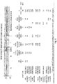
- Fig. 1 shows an example of a SiGe EPI structure in accordance with the present invention in which a thin layer of transit buffer SiGe is inserted between the 3 ⁇ m SOI waveguide and the SiGe buffer layer that is for the SiGe MQW.
- the transit buffer SiGe layer shown has a germanium content of 20% (Si 0.8 Ge 0.2 ).
- this transit buffer SiGe layer may have a germanium content ranging from 5% (Si 0.95 Ge 0.05 ) to 50% (Si 0.5 Ge 0.5 ) and a thickness ranging from 400nm to 1000nm.
- the waveguide evanescent coupling structure brings light from the SOI waveguide (which may be a 3 ⁇ m SOI waveguide) to a SiGe MQW waveguide in the following steps:
- the QCSE EAM consists of two coupling regions, which have two waveguide evanescent coupling structures and one taper structure, and one active region between the two coupling regions
- the active region preferably has the same waveguide structure as the SiGe MQW waveguide.
- Si waveguide (which may be a 3um Si waveguide) travels through the first coupling region to reach the active region.
- the light goes through the second coupling region back to a/the Si waveguide (which may be a 3 ⁇ m Si waveguide).
- the first example can be seen in the 3D views shown in Fig.2A and Fig.2B and also in the top views as shown in Fig.3A (GS electrodes) and Fig.3B (GSG electrodes).
- the taper structure comprises 3 segments to expand the optical mode of buffer waveguide to the optical mode of SiGe MQW waveguide.
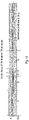
- An example of measurements for the entire device is shown in Fig.4 and a section view of the device is shown in Fig.5 .
- the simulation results for device design #1 at 1.3 ⁇ m wavelength for TE mode are below: insertion loss 4.87dB, extinction ratio 4.16dB and link penalty 9.97dB.
- the second example (device design #2 based on EPI design #1) can be seen in the 3D views shown in Fig.6A and Fig.6B and also in the top views as shown in Fig.7A (GS electrodes) and Fig.7B (GSG electrodes).
- the taper structure comprises 4 segments to expand the optical mode of buffer waveguide to the optical mode of SiGe MQW waveguide.
- An example of measurements for the entire device of the second example (device design #2 based on EPI design #1) is shown in Fig.8 and a section view of the device is shown in Fig.9 .
- the simulation results for device design #2 at 1.3 ⁇ m wavelength for TE mode are below: insertion loss 4.43dB, extinction ratio 4.16dB and link penalty 9.53dB.
- FIG. 10-12 An example (EPI design #2) and an associated device design #3 is shown in Figs. 10-12 . This embodiment differs from that of Fig.1 (EPI design #1) in that:
- devices including the EPI design of the second embodiment may be fabricated with:
- the taper structure comprises 4 segments to expand the optical mode of buffer waveguide to the optical mode of SiGe MQW waveguide.
- the simulation results for device design #3 at 1.3 ⁇ m wavelength for TE mode are below: insertion loss 4.87dB, extinction ratio 4.16dB and link penalty 9.97dB.
- FIG. 13-15 A third embodiment (EPI design #3) of the present invention and an associated device design #4 is shown in Figs. 13-15 . This embodiment differs from that of Fig.1 (EPI design #1) in that:
- devices including the EPI design of the third embodiment may be fabricated with:
- the taper structure comprises 4 segments to expand the optical mode of buffer waveguide to the optical mode of SiGe MQW waveguide.
- the simulation results for device design #4 at 1.3 ⁇ m wavelength for TE mode are below: insertion loss 4.66dB, extinction ratio 4.16dB and link penalty 9.76dB.
- Fig.16 An example of in input (and/or output waveguide) for coupling to any one of the EPI regions described herein is shown in Fig.16 . In some embodiments, this may take the form of a 3 ⁇ m SOI waveguide.
- Typical optical transition from 3 ⁇ m SOI waveguide to SiGe MQW waveguide simulation result at i .3 ⁇ m wavelength is shown in Fig. 17 for a half device structure.
- the device is symmetric, so the half structure simulation enabled relevant information to be achieved whilst conserving computer space.
- Fig.18 shows another example of a device design; "device design #5".
- This device design is could contain any one of the EPI structures of the embodiments (EPI design #1, EPI design #2 and EPI design #3) shown in Fig.1 , Fig.10 and Fig.13 .
- the taper structure of device design #5 comprises 2 segments which act to expand the optical mode of buffer waveguide to the optical mode of SiGe MQW waveguide.
- An advantage of using such a taper structure with 2 segments is the ease of device fabrication process with fewer processing steps.
- Fig.19 shows the section view of design #5 along the middle line KK'.
- EPI design #1B A fourth embodiment (EPI design #1B) of the present invention and associated device design is shown in Fig. 20-21 .
- the MQW region comprises a main section in the main body of the active region, but also includes at least one tapered portion of MQW material which extends from the main body of the active material forming active tapered portions overlaying the tapered layers underneath.
- the tapered portions of the MQW material therefore extend outwards from the main body of the active region (marked "E") into at least the active mode expander region (marked "D").
- a fifth embodiment (EPI design #1B (Modified)) of the present invention is shown in Fig. 22 . in which a thin layer of transit buffer SiGe is inserted between the 3 ⁇ m SOI waveguide and the SiGe buffer layer that is for the SiGe MQE. Broadly it is a modified version of the EPI structure corresponding with the device in Fig. 20 and 21 .
- EPI design #1C Modified
- FIG. 23 - 25 A sixth embodiment (EPI design #1C (Modified)) of the present invention and associated device design is shown in Fig. 23 - 25 .
- FIG. 24 An example of measurements of the entire device is shown in Fig. 24 , and a section view of the device is shown in Fig. 25 .
- the active region could contain an EPI structure as shown in Fig. 22 or Fig. 23 .
- Fig. 23 shows an example of a SiGe EPI structure in accordance with the present invention in which a thin layer of transit buffer SiGe is inserted between the 3 ⁇ m SOI waveguide and the SiGe buffer layer that is for the SiGe MQW.
- a further difference between the device shown in Fig. 4 and those shown in Figs. 20 and 24 is that the electrodes of Figs. 20 and 24 which are in contact with a surface of the active region opposite the coupler extend beyond the active region in a direction towards their respective taper regions.
- the electrodes in Figs. 20 and 24 have a length in the direction towards the taper region which is greater than 2.5 ⁇ m.
Landscapes
- Physics & Mathematics (AREA)
- Nonlinear Science (AREA)
- General Physics & Mathematics (AREA)
- Optics & Photonics (AREA)
- Engineering & Computer Science (AREA)
- Power Engineering (AREA)
- Microelectronics & Electronic Packaging (AREA)
- Optical Modulation, Optical Deflection, Nonlinear Optics, Optical Demodulation, Optical Logic Elements (AREA)
Claims (14)
- Elektroabsorptionsmodulator, der Folgendes umfasst:einen SOI-Wellenleiter;eine aktive Region, wobei die aktive Region eine SiGe-Multiquantentopf- (MQW-) Region umfasst; undeine evaneszente Kopplungsstruktur zum Koppeln des SOI-Wellenleiters mit der aktiven Region;wobei die Kopplungsstruktur Folgendes umfasst:eine SiGe-Transitwellenleiter-Kopplungsregion;eine SiGe-Pufferwellenleiter-Kopplungsregion, dotiert mit Dotiermitteln vom P-Typ; undeine Verjüngungsregion;wobei die Transitwellenleiter-Kopplungsregion Licht zwischen dem SOI-Wellenleiter und der Pufferwellenleiter-Kopplungsregion koppelt; und wobei die Pufferwellenleiter-Kopplungsregion Licht zwischen der Transitwellenleiterregion und der aktiven Region über die Verjüngungsregion koppelt, dadurch gekennzeichnet, dass:die sich verjüngende Transitwellenleiter-Kopplungsregion einen ersten verjüngten Abschnitt und einen zweiten Abschnitt umfasst;der Pufferwellenleiter eine verjüngte Kopplungsregion umfasst, die auf dem zweiten Abschnitt des Transitwellenleiters angeordnet ist; undder Brechungsindex der Transitwellenleiter-Kopplungsregion kleiner ist als jener der Pufferwellenleiter-Kopplungsregion.
- Elektroabsorptionsmodulator nach Anspruch 1, wobei die Konzentration von Dotiermittel vom P-Typ des Pufferwellenleiters 1 x 1018 cm-3 beträgt und Si0.24Ge0.76 umfasst.
- Elektroabsorptionsmodulator nach Anspruch 1 oder Anspruch 2, wobei die Verjüngungsregion einen Multisegment-Modusexpander umfasst.
- Elektroabsorptionsmodulator nach einem der vorangegangenen Ansprüche, wobei die Multiquantentopfregion eine Ge/SiGe-Multiquantentopfregion ist und/oder wobei der Transitwellenleiter einen Brechungsindex aufweist, der größer ist als jener des SOI-Wellenleiters, aber kleiner als jener des Pufferwellenleiters.
- Elektroabsorptionsmodulator nach einem der vorangegangenen Ansprüche, wobei:der SOI-Wellenleiter ein 3-µm-Wellenleiter ist;der Transitwellenleiter eine Dicke von nicht mehr als 400 nm aufweist; undder Pufferwellenleiter eine Dicke von nicht mehr als 400 nm aufweist.
- Elektroabsorptionsmodulator nach Anspruch 5, wobei der Transitpufferwellenleiter eine Dicke von nicht mehr als 600 nm aufweist und/oder wobei der Transitwellenleiter eine Dicke von nicht mehr als 800 nm aufweist.
- Elektroabsorptionsmodulator nach einem der Ansprüche 1 bis 6,
wobei die aktive Region Folgendes umfasst:eine P-dotierte Region zwischen der Pufferschicht und der unteren Oberfläche einer Beabstandungsschicht unterhalb eines Multiquantentopfs; undeine N-dotierte Region, die an der oberen Oberfläche einer Beabstandungsschicht auf dem Multiquantentopf angeordnet ist, wobei der Elektroabsorptionsmodulator ferner mehrere N-Typ-dotierte Schichten mit verschiedenen Germaniumzusammensetzungen und Dotierungskonzentrationen umfasst. - Elektroabsorptionsmodulator nach einem der vorangegangenen Ansprüche, wobei die Wellenleiterplatte der P-Typ-Schicht in der aktiven Region mit Ionenimplantation P-dotiert ist, gefolgt von einem RTA-Verfahren und/oder wobei die Elektroden in einer Masse-Signal-(GS-) Konfiguration angeordnet sind, wobei eine Masseelektrode an einer der aktiven Region der Signalelektrode entgegengesetzten Seite angeordnet ist.
- Elektroabsorptionsmodulator nach einem der vorangegangenen Ansprüche, wobei die Elektroden in einer Masse-Signal-Masse- (GSG-) Konfiguration angeordnet sind, wobei eine erste Masseelektrode und eine zweite Masseelektrode auf derselben Seite der aktiven Region wie die Signalelektrode angeordnet sind und/oder wobei die Multiquantentopfregion zumindest 5 Quantentöpfe umfasst.
- Elektroabsorptionsmodulator nach einem der vorangegangenen Ansprüche, wobei die Multiquantentopfregion entweder 5, 7 oder 10 Quantentöpfe umfasst.
- Elektroabsorptionsmodulator nach einem der vorangegangenen Ansprüche, wobei die Multiquantentopfregion nicht mehr als 240 nm dick ist und vorzugsweise nicht mehr als 232 nm dick ist.
- Elektroabsorptionsmodulator nach einem der vorangegangenen Ansprüche, wobei ein Abstand zwischen entsprechenden Paaren der Quantentöpfe im Bereich von 10 nm bis 20 nm liegt und/oder wobei jeder der Multiquantentöpfe eine Dicke im Bereich von 5 nm bis 15 nm aufweist.
- Elektroabsorptionsmodulator nach einem der vorangegangenen Ansprüche, der ferner eine Metallelektrode in Kontakt mit einer Oberfläche der dem Koppler entgegengesetzten aktiven Region umfasst, wobei die MQW-Region zumindest einen verjüngten Abschnitt aus MQW-Material aufweist, der sich in die Verjüngungsregion erstreckt; und wobei sich die Metallelektrode bis zur verjüngten Region aus MQW-Material erstreckt.
- Elektroabsorptionsmodulator nach Anspruch 13, wobei die Elektrode eine Länge in Richtung der Verjüngungsregion aufweist, die größer ist als 2,5 µm), und/oder wobei die aktive Region eine N-dotierte Region umfasst, die oberhalb der oberen Oberfläche einer Beabstandungsschicht auf der Multiquantentopfregion angeordnet ist, und wobei die N-dotierte Region Si0,9Ge0,1 umfasst.
Applications Claiming Priority (2)
| Application Number | Priority Date | Filing Date | Title |
|---|---|---|---|
| US201662359595P | 2016-07-07 | 2016-07-07 | |
| PCT/IT2017/000004 WO2018008046A1 (en) | 2016-07-07 | 2017-01-16 | Quantum confined stark effect electro absorption modulator on a soi platform |
Publications (2)
| Publication Number | Publication Date |
|---|---|
| EP3513246A1 EP3513246A1 (de) | 2019-07-24 |
| EP3513246B1 true EP3513246B1 (de) | 2022-06-08 |
Family
ID=58410409
Family Applications (2)
| Application Number | Title | Priority Date | Filing Date |
|---|---|---|---|
| EP17713472.3A Active EP3513246B1 (de) | 2016-07-07 | 2017-01-16 | Quantenbegrenzter stark-effekt-elektroabsorptionsmodulator auf einer soi-plattform |
| EP17740464.7A Active EP3513247B1 (de) | 2016-07-07 | 2017-07-07 | Quantenbegrenzter stark wirkender elektroabsorptionsmodulator auf einer soi-plattform |
Family Applications After (1)
| Application Number | Title | Priority Date | Filing Date |
|---|---|---|---|
| EP17740464.7A Active EP3513247B1 (de) | 2016-07-07 | 2017-07-07 | Quantenbegrenzter stark wirkender elektroabsorptionsmodulator auf einer soi-plattform |
Country Status (4)
| Country | Link |
|---|---|
| US (2) | US20190235286A1 (de) |
| EP (2) | EP3513246B1 (de) |
| CN (2) | CN210005813U (de) |
| WO (2) | WO2018008046A1 (de) |
Families Citing this family (5)
| Publication number | Priority date | Publication date | Assignee | Title |
|---|---|---|---|---|
| CN210005813U (zh) | 2016-07-07 | 2020-01-31 | 洛克利光子有限公司 | Soi平台上的量子限制斯塔克效应电吸收调制器 |
| US10809548B2 (en) | 2016-10-26 | 2020-10-20 | Juniper Networks, Inc. | Dissipating heat from an active region of an optical device |
| CN108508635B (zh) * | 2018-04-10 | 2020-08-25 | 中国科学院半导体研究所 | 基于SiGe材料的电调谐有源波导结构以及应用其的MZI结构 |
| CN110687694A (zh) * | 2018-07-04 | 2020-01-14 | 上海新微技术研发中心有限公司 | 电吸收调制器及半导体器件 |
| US12176677B2 (en) * | 2019-12-27 | 2024-12-24 | Openlight Photonics, Inc. | Electro-absorption modulator with improved photocurrent uniformity |
Family Cites Families (6)
| Publication number | Priority date | Publication date | Assignee | Title |
|---|---|---|---|---|
| JP3913161B2 (ja) * | 2002-11-14 | 2007-05-09 | アンリツ株式会社 | 光導波路型半導体デバイス |
| US8401345B2 (en) * | 2010-06-16 | 2013-03-19 | Oracle America, Inc. | Optical modulator with three-dimensional waveguide tapers |
| CN102169243A (zh) * | 2011-04-28 | 2011-08-31 | 中国科学院半导体研究所 | 亚微米波导型Ge量子阱电光调制器 |
| WO2014200920A2 (en) * | 2013-06-09 | 2014-12-18 | Seng-Tiong Ho | Ultra-low-voltage broad-modulation-bandwidth low-optical-loss optical intensity or phase modulators |
| EP3091381B1 (de) * | 2015-05-07 | 2020-07-01 | IMEC vzw | Verfahren zur herstellung photonischer integrierter schaltungen mit heterogenem iii-v-silicium |
| CN210005813U (zh) * | 2016-07-07 | 2020-01-31 | 洛克利光子有限公司 | Soi平台上的量子限制斯塔克效应电吸收调制器 |
-
2017
- 2017-01-16 CN CN201790001047.7U patent/CN210005813U/zh active Active
- 2017-01-16 EP EP17713472.3A patent/EP3513246B1/de active Active
- 2017-01-16 WO PCT/IT2017/000004 patent/WO2018008046A1/en not_active Ceased
- 2017-01-16 US US16/315,510 patent/US20190235286A1/en not_active Abandoned
- 2017-07-07 EP EP17740464.7A patent/EP3513247B1/de active Active
- 2017-07-07 US US16/315,569 patent/US10788688B2/en active Active
- 2017-07-07 CN CN201780042308.4A patent/CN109791314B/zh active Active
- 2017-07-07 WO PCT/GB2017/051998 patent/WO2018007824A1/en not_active Ceased
Also Published As
| Publication number | Publication date |
|---|---|
| CN109791314B (zh) | 2022-08-30 |
| WO2018008046A1 (en) | 2018-01-11 |
| CN210005813U (zh) | 2020-01-31 |
| EP3513247A1 (de) | 2019-07-24 |
| EP3513246A1 (de) | 2019-07-24 |
| CN109791314A (zh) | 2019-05-21 |
| US20190324299A1 (en) | 2019-10-24 |
| US10788688B2 (en) | 2020-09-29 |
| US20190235286A1 (en) | 2019-08-01 |
| EP3513247B1 (de) | 2022-06-08 |
| WO2018007824A1 (en) | 2018-01-11 |
Similar Documents
| Publication | Publication Date | Title |
|---|---|---|
| EP3513247B1 (de) | Quantenbegrenzter stark wirkender elektroabsorptionsmodulator auf einer soi-plattform | |
| US10831043B2 (en) | Electro-optically active device | |
| US10222677B2 (en) | Optoelectronic device | |
| US10216059B2 (en) | Waveguide modulator structures | |
| EP3545356B1 (de) | Elektrooptisch aktive vorrichtung | |
| US8149493B2 (en) | Electro-optic silicon modulator | |
| US10401656B2 (en) | Optoelectronic device | |
| US20190179177A1 (en) | Optoelectronic device | |
| JP5565148B2 (ja) | 半導体光素子 | |
| EP3961727A2 (de) | Diode mit lichtempfindlichem intrinsischem bereich | |
| JP2011203382A (ja) | 半導体光素子 | |
| US10921616B2 (en) | Optoelectronic device | |
| US20120280347A1 (en) | Waveguide photo-detector | |
| US20120294563A1 (en) | Electro-optic silicon modulator | |
| JP2011091163A (ja) | 半導体集積素子 | |
| US10976490B2 (en) | Optoelectronic device and method of manufacturing the same | |
| US12155012B2 (en) | Nanowire optical device | |
| GB2584501A (en) | Electro-optically active device | |
| GB2556131A (en) | Quantum confined stark effect electroabsorption modulator on a soi platform | |
| Badr et al. | All-silicon directional coupler electro-optic modulator utilizing transparent conducting oxides | |
| CN120882173A (zh) | 具有载流子屏蔽缓解的光电二极管 |
Legal Events
| Date | Code | Title | Description |
|---|---|---|---|
| STAA | Information on the status of an ep patent application or granted ep patent |
Free format text: STATUS: UNKNOWN |
|
| STAA | Information on the status of an ep patent application or granted ep patent |
Free format text: STATUS: THE INTERNATIONAL PUBLICATION HAS BEEN MADE |
|
| PUAI | Public reference made under article 153(3) epc to a published international application that has entered the european phase |
Free format text: ORIGINAL CODE: 0009012 |
|
| STAA | Information on the status of an ep patent application or granted ep patent |
Free format text: STATUS: REQUEST FOR EXAMINATION WAS MADE |
|
| 17P | Request for examination filed |
Effective date: 20190524 |
|
| AK | Designated contracting states |
Kind code of ref document: A1 Designated state(s): AL AT BE BG CH CY CZ DE DK EE ES FI FR GB GR HR HU IE IS IT LI LT LU LV MC MK MT NL NO PL PT RO RS SE SI SK SM TR |
|
| AX | Request for extension of the european patent |
Extension state: BA ME |
|
| DAV | Request for validation of the european patent (deleted) | ||
| DAX | Request for extension of the european patent (deleted) | ||
| STAA | Information on the status of an ep patent application or granted ep patent |
Free format text: STATUS: EXAMINATION IS IN PROGRESS |
|
| 17Q | First examination report despatched |
Effective date: 20200708 |
|
| GRAP | Despatch of communication of intention to grant a patent |
Free format text: ORIGINAL CODE: EPIDOSNIGR1 |
|
| STAA | Information on the status of an ep patent application or granted ep patent |
Free format text: STATUS: GRANT OF PATENT IS INTENDED |
|
| INTG | Intention to grant announced |
Effective date: 20211220 |
|
| GRAS | Grant fee paid |
Free format text: ORIGINAL CODE: EPIDOSNIGR3 |
|
| GRAA | (expected) grant |
Free format text: ORIGINAL CODE: 0009210 |
|
| STAA | Information on the status of an ep patent application or granted ep patent |
Free format text: STATUS: THE PATENT HAS BEEN GRANTED |
|
| RAP3 | Party data changed (applicant data changed or rights of an application transferred) |
Owner name: POLITECNICO DI MILANO Owner name: ROCKLEY PHOTONICS LIMITED |
|
| RIN1 | Information on inventor provided before grant (corrected) |
Inventor name: BALLABIO, ANDREA Inventor name: FRIGERIO, JACOPO Inventor name: ISELLA, GIOVANNI Inventor name: YU, GUOMIN |
|
| AK | Designated contracting states |
Kind code of ref document: B1 Designated state(s): AL AT BE BG CH CY CZ DE DK EE ES FI FR GB GR HR HU IE IS IT LI LT LU LV MC MK MT NL NO PL PT RO RS SE SI SK SM TR |
|
| REG | Reference to a national code |
Ref country code: AT Ref legal event code: REF Ref document number: 1497323 Country of ref document: AT Kind code of ref document: T Effective date: 20220615 Ref country code: CH Ref legal event code: EP |
|
| REG | Reference to a national code |
Ref country code: DE Ref legal event code: R096 Ref document number: 602017058267 Country of ref document: DE |
|
| REG | Reference to a national code |
Ref country code: IE Ref legal event code: FG4D |
|
| REG | Reference to a national code |
Ref country code: LT Ref legal event code: MG9D |
|
| REG | Reference to a national code |
Ref country code: NL Ref legal event code: MP Effective date: 20220608 |
|
| PG25 | Lapsed in a contracting state [announced via postgrant information from national office to epo] |
Ref country code: SE Free format text: LAPSE BECAUSE OF FAILURE TO SUBMIT A TRANSLATION OF THE DESCRIPTION OR TO PAY THE FEE WITHIN THE PRESCRIBED TIME-LIMIT Effective date: 20220608 Ref country code: NO Free format text: LAPSE BECAUSE OF FAILURE TO SUBMIT A TRANSLATION OF THE DESCRIPTION OR TO PAY THE FEE WITHIN THE PRESCRIBED TIME-LIMIT Effective date: 20220908 Ref country code: LT Free format text: LAPSE BECAUSE OF FAILURE TO SUBMIT A TRANSLATION OF THE DESCRIPTION OR TO PAY THE FEE WITHIN THE PRESCRIBED TIME-LIMIT Effective date: 20220608 Ref country code: HR Free format text: LAPSE BECAUSE OF FAILURE TO SUBMIT A TRANSLATION OF THE DESCRIPTION OR TO PAY THE FEE WITHIN THE PRESCRIBED TIME-LIMIT Effective date: 20220608 Ref country code: GR Free format text: LAPSE BECAUSE OF FAILURE TO SUBMIT A TRANSLATION OF THE DESCRIPTION OR TO PAY THE FEE WITHIN THE PRESCRIBED TIME-LIMIT Effective date: 20220909 Ref country code: FI Free format text: LAPSE BECAUSE OF FAILURE TO SUBMIT A TRANSLATION OF THE DESCRIPTION OR TO PAY THE FEE WITHIN THE PRESCRIBED TIME-LIMIT Effective date: 20220608 Ref country code: ES Free format text: LAPSE BECAUSE OF FAILURE TO SUBMIT A TRANSLATION OF THE DESCRIPTION OR TO PAY THE FEE WITHIN THE PRESCRIBED TIME-LIMIT Effective date: 20220608 Ref country code: BG Free format text: LAPSE BECAUSE OF FAILURE TO SUBMIT A TRANSLATION OF THE DESCRIPTION OR TO PAY THE FEE WITHIN THE PRESCRIBED TIME-LIMIT Effective date: 20220908 |
|
| REG | Reference to a national code |
Ref country code: AT Ref legal event code: MK05 Ref document number: 1497323 Country of ref document: AT Kind code of ref document: T Effective date: 20220608 |
|
| PG25 | Lapsed in a contracting state [announced via postgrant information from national office to epo] |
Ref country code: RS Free format text: LAPSE BECAUSE OF FAILURE TO SUBMIT A TRANSLATION OF THE DESCRIPTION OR TO PAY THE FEE WITHIN THE PRESCRIBED TIME-LIMIT Effective date: 20220608 Ref country code: LV Free format text: LAPSE BECAUSE OF FAILURE TO SUBMIT A TRANSLATION OF THE DESCRIPTION OR TO PAY THE FEE WITHIN THE PRESCRIBED TIME-LIMIT Effective date: 20220608 |
|
| PG25 | Lapsed in a contracting state [announced via postgrant information from national office to epo] |
Ref country code: NL Free format text: LAPSE BECAUSE OF FAILURE TO SUBMIT A TRANSLATION OF THE DESCRIPTION OR TO PAY THE FEE WITHIN THE PRESCRIBED TIME-LIMIT Effective date: 20220608 |
|
| PG25 | Lapsed in a contracting state [announced via postgrant information from national office to epo] |
Ref country code: SM Free format text: LAPSE BECAUSE OF FAILURE TO SUBMIT A TRANSLATION OF THE DESCRIPTION OR TO PAY THE FEE WITHIN THE PRESCRIBED TIME-LIMIT Effective date: 20220608 Ref country code: SK Free format text: LAPSE BECAUSE OF FAILURE TO SUBMIT A TRANSLATION OF THE DESCRIPTION OR TO PAY THE FEE WITHIN THE PRESCRIBED TIME-LIMIT Effective date: 20220608 Ref country code: RO Free format text: LAPSE BECAUSE OF FAILURE TO SUBMIT A TRANSLATION OF THE DESCRIPTION OR TO PAY THE FEE WITHIN THE PRESCRIBED TIME-LIMIT Effective date: 20220608 Ref country code: PT Free format text: LAPSE BECAUSE OF FAILURE TO SUBMIT A TRANSLATION OF THE DESCRIPTION OR TO PAY THE FEE WITHIN THE PRESCRIBED TIME-LIMIT Effective date: 20221010 Ref country code: EE Free format text: LAPSE BECAUSE OF FAILURE TO SUBMIT A TRANSLATION OF THE DESCRIPTION OR TO PAY THE FEE WITHIN THE PRESCRIBED TIME-LIMIT Effective date: 20220608 Ref country code: CZ Free format text: LAPSE BECAUSE OF FAILURE TO SUBMIT A TRANSLATION OF THE DESCRIPTION OR TO PAY THE FEE WITHIN THE PRESCRIBED TIME-LIMIT Effective date: 20220608 Ref country code: AT Free format text: LAPSE BECAUSE OF FAILURE TO SUBMIT A TRANSLATION OF THE DESCRIPTION OR TO PAY THE FEE WITHIN THE PRESCRIBED TIME-LIMIT Effective date: 20220608 |
|
| PG25 | Lapsed in a contracting state [announced via postgrant information from national office to epo] |
Ref country code: PL Free format text: LAPSE BECAUSE OF FAILURE TO SUBMIT A TRANSLATION OF THE DESCRIPTION OR TO PAY THE FEE WITHIN THE PRESCRIBED TIME-LIMIT Effective date: 20220608 Ref country code: IS Free format text: LAPSE BECAUSE OF FAILURE TO SUBMIT A TRANSLATION OF THE DESCRIPTION OR TO PAY THE FEE WITHIN THE PRESCRIBED TIME-LIMIT Effective date: 20221008 |
|
| REG | Reference to a national code |
Ref country code: DE Ref legal event code: R097 Ref document number: 602017058267 Country of ref document: DE |
|
| PG25 | Lapsed in a contracting state [announced via postgrant information from national office to epo] |
Ref country code: AL Free format text: LAPSE BECAUSE OF FAILURE TO SUBMIT A TRANSLATION OF THE DESCRIPTION OR TO PAY THE FEE WITHIN THE PRESCRIBED TIME-LIMIT Effective date: 20220608 |
|
| PLBE | No opposition filed within time limit |
Free format text: ORIGINAL CODE: 0009261 |
|
| STAA | Information on the status of an ep patent application or granted ep patent |
Free format text: STATUS: NO OPPOSITION FILED WITHIN TIME LIMIT |
|
| PG25 | Lapsed in a contracting state [announced via postgrant information from national office to epo] |
Ref country code: DK Free format text: LAPSE BECAUSE OF FAILURE TO SUBMIT A TRANSLATION OF THE DESCRIPTION OR TO PAY THE FEE WITHIN THE PRESCRIBED TIME-LIMIT Effective date: 20220608 |
|
| 26N | No opposition filed |
Effective date: 20230310 |
|
| PG25 | Lapsed in a contracting state [announced via postgrant information from national office to epo] |
Ref country code: SI Free format text: LAPSE BECAUSE OF FAILURE TO SUBMIT A TRANSLATION OF THE DESCRIPTION OR TO PAY THE FEE WITHIN THE PRESCRIBED TIME-LIMIT Effective date: 20220608 |
|
| REG | Reference to a national code |
Ref country code: DE Ref legal event code: R119 Ref document number: 602017058267 Country of ref document: DE |
|
| REG | Reference to a national code |
Ref country code: CH Ref legal event code: PL |
|
| GBPC | Gb: european patent ceased through non-payment of renewal fee |
Effective date: 20230116 |
|
| PG25 | Lapsed in a contracting state [announced via postgrant information from national office to epo] |
Ref country code: LU Free format text: LAPSE BECAUSE OF NON-PAYMENT OF DUE FEES Effective date: 20230116 |
|
| REG | Reference to a national code |
Ref country code: BE Ref legal event code: MM Effective date: 20230131 |
|
| PG25 | Lapsed in a contracting state [announced via postgrant information from national office to epo] |
Ref country code: LI Free format text: LAPSE BECAUSE OF NON-PAYMENT OF DUE FEES Effective date: 20230131 Ref country code: GB Free format text: LAPSE BECAUSE OF NON-PAYMENT OF DUE FEES Effective date: 20230116 Ref country code: DE Free format text: LAPSE BECAUSE OF NON-PAYMENT OF DUE FEES Effective date: 20230801 Ref country code: CH Free format text: LAPSE BECAUSE OF NON-PAYMENT OF DUE FEES Effective date: 20230131 |
|
| PG25 | Lapsed in a contracting state [announced via postgrant information from national office to epo] |
Ref country code: FR Free format text: LAPSE BECAUSE OF NON-PAYMENT OF DUE FEES Effective date: 20230131 Ref country code: BE Free format text: LAPSE BECAUSE OF NON-PAYMENT OF DUE FEES Effective date: 20230131 |
|
| PG25 | Lapsed in a contracting state [announced via postgrant information from national office to epo] |
Ref country code: IT Free format text: LAPSE BECAUSE OF FAILURE TO SUBMIT A TRANSLATION OF THE DESCRIPTION OR TO PAY THE FEE WITHIN THE PRESCRIBED TIME-LIMIT Effective date: 20220608 Ref country code: IE Free format text: LAPSE BECAUSE OF NON-PAYMENT OF DUE FEES Effective date: 20230116 |
|
| PG25 | Lapsed in a contracting state [announced via postgrant information from national office to epo] |
Ref country code: MC Free format text: LAPSE BECAUSE OF FAILURE TO SUBMIT A TRANSLATION OF THE DESCRIPTION OR TO PAY THE FEE WITHIN THE PRESCRIBED TIME-LIMIT Effective date: 20220608 |
|
| PG25 | Lapsed in a contracting state [announced via postgrant information from national office to epo] |
Ref country code: MC Free format text: LAPSE BECAUSE OF FAILURE TO SUBMIT A TRANSLATION OF THE DESCRIPTION OR TO PAY THE FEE WITHIN THE PRESCRIBED TIME-LIMIT Effective date: 20220608 |
|
| PG25 | Lapsed in a contracting state [announced via postgrant information from national office to epo] |
Ref country code: BG Free format text: LAPSE BECAUSE OF FAILURE TO SUBMIT A TRANSLATION OF THE DESCRIPTION OR TO PAY THE FEE WITHIN THE PRESCRIBED TIME-LIMIT Effective date: 20220608 |
|
| PG25 | Lapsed in a contracting state [announced via postgrant information from national office to epo] |
Ref country code: BG Free format text: LAPSE BECAUSE OF FAILURE TO SUBMIT A TRANSLATION OF THE DESCRIPTION OR TO PAY THE FEE WITHIN THE PRESCRIBED TIME-LIMIT Effective date: 20220608 |
|
| PG25 | Lapsed in a contracting state [announced via postgrant information from national office to epo] |
Ref country code: CY Free format text: LAPSE BECAUSE OF FAILURE TO SUBMIT A TRANSLATION OF THE DESCRIPTION OR TO PAY THE FEE WITHIN THE PRESCRIBED TIME-LIMIT; INVALID AB INITIO Effective date: 20170116 |
|
| PG25 | Lapsed in a contracting state [announced via postgrant information from national office to epo] |
Ref country code: HU Free format text: LAPSE BECAUSE OF FAILURE TO SUBMIT A TRANSLATION OF THE DESCRIPTION OR TO PAY THE FEE WITHIN THE PRESCRIBED TIME-LIMIT; INVALID AB INITIO Effective date: 20170116 |
|
| PG25 | Lapsed in a contracting state [announced via postgrant information from national office to epo] |
Ref country code: TR Free format text: LAPSE BECAUSE OF FAILURE TO SUBMIT A TRANSLATION OF THE DESCRIPTION OR TO PAY THE FEE WITHIN THE PRESCRIBED TIME-LIMIT Effective date: 20220608 |