EP3512193A1 - Imaging element and driving method, and electronic apparatus - Google Patents
Imaging element and driving method, and electronic apparatus Download PDFInfo
- Publication number
- EP3512193A1 EP3512193A1 EP17848561.1A EP17848561A EP3512193A1 EP 3512193 A1 EP3512193 A1 EP 3512193A1 EP 17848561 A EP17848561 A EP 17848561A EP 3512193 A1 EP3512193 A1 EP 3512193A1
- Authority
- EP
- European Patent Office
- Prior art keywords
- pixel
- unit
- inter
- conversion
- image processing
- Prior art date
- Legal status (The legal status is an assumption and is not a legal conclusion. Google has not performed a legal analysis and makes no representation as to the accuracy of the status listed.)
- Granted
Links
Images


Classifications
-
- G—PHYSICS
- G06—COMPUTING OR CALCULATING; COUNTING
- G06T—IMAGE DATA PROCESSING OR GENERATION, IN GENERAL
- G06T1/00—General purpose image data processing
- G06T1/20—Processor architectures; Processor configuration, e.g. pipelining
-
- G—PHYSICS
- G06—COMPUTING OR CALCULATING; COUNTING
- G06T—IMAGE DATA PROCESSING OR GENERATION, IN GENERAL
- G06T1/00—General purpose image data processing
- G06T1/60—Memory management
-
- H—ELECTRICITY
- H04—ELECTRIC COMMUNICATION TECHNIQUE
- H04N—PICTORIAL COMMUNICATION, e.g. TELEVISION
- H04N25/00—Circuitry of solid-state image sensors [SSIS]; Control thereof
-
- H—ELECTRICITY
- H04—ELECTRIC COMMUNICATION TECHNIQUE
- H04N—PICTORIAL COMMUNICATION, e.g. TELEVISION
- H04N25/00—Circuitry of solid-state image sensors [SSIS]; Control thereof
- H04N25/40—Extracting pixel data from image sensors by controlling scanning circuits, e.g. by modifying the number of pixels sampled or to be sampled
-
- H—ELECTRICITY
- H04—ELECTRIC COMMUNICATION TECHNIQUE
- H04N—PICTORIAL COMMUNICATION, e.g. TELEVISION
- H04N25/00—Circuitry of solid-state image sensors [SSIS]; Control thereof
- H04N25/70—SSIS architectures; Circuits associated therewith
- H04N25/703—SSIS architectures incorporating pixels for producing signals other than image signals
- H04N25/707—Pixels for event detection
-
- H—ELECTRICITY
- H04—ELECTRIC COMMUNICATION TECHNIQUE
- H04N—PICTORIAL COMMUNICATION, e.g. TELEVISION
- H04N25/00—Circuitry of solid-state image sensors [SSIS]; Control thereof
- H04N25/70—SSIS architectures; Circuits associated therewith
- H04N25/703—SSIS architectures incorporating pixels for producing signals other than image signals
- H04N25/708—Pixels for edge detection
-
- H—ELECTRICITY
- H04—ELECTRIC COMMUNICATION TECHNIQUE
- H04N—PICTORIAL COMMUNICATION, e.g. TELEVISION
- H04N25/00—Circuitry of solid-state image sensors [SSIS]; Control thereof
- H04N25/70—SSIS architectures; Circuits associated therewith
- H04N25/76—Addressed sensors, e.g. MOS or CMOS sensors
-
- H—ELECTRICITY
- H04—ELECTRIC COMMUNICATION TECHNIQUE
- H04N—PICTORIAL COMMUNICATION, e.g. TELEVISION
- H04N25/00—Circuitry of solid-state image sensors [SSIS]; Control thereof
- H04N25/70—SSIS architectures; Circuits associated therewith
- H04N25/76—Addressed sensors, e.g. MOS or CMOS sensors
- H04N25/78—Readout circuits for addressed sensors, e.g. output amplifiers or A/D converters
-
- H—ELECTRICITY
- H04—ELECTRIC COMMUNICATION TECHNIQUE
- H04N—PICTORIAL COMMUNICATION, e.g. TELEVISION
- H04N25/00—Circuitry of solid-state image sensors [SSIS]; Control thereof
- H04N25/70—SSIS architectures; Circuits associated therewith
- H04N25/79—Arrangements of circuitry being divided between different or multiple substrates, chips or circuit boards, e.g. stacked image sensors
Definitions
- the present disclosure relates to an image sensor and a driving method, and an electronic apparatus, and particularly relates to an image sensor and a driving method, and an electronic apparatus that are capable of performing inter-pixel image processing with lower latency and higher speed.
- a vision chip obtained by integrating an imaging portion and an image processing portion of an image sensor onto a chip has been under research.
- an imaging device has been known in which, in regard to a plurality of pixels two-dimensionally arranged in a matrix and having a photoelectric conversion function, one image processing circuit is disposed for one pixel, and image processing is performed in parallel.
- image processing can be performed with higher speed and low latency.
- an image processing circuit generally occupies a larger area than a pixel size, which makes it difficult to make a pixel portion for photoelectric conversion large; thus, it has been difficult to obtain sufficient sensitivity characteristics.
- an area of one unit pixel including an image processing circuit and a pixel is large, which makes it difficult to increase the number of pixels.
- Patent Literature 1 discloses large-scale integration (LSI) for pattern signal processing that employs a configuration in which one processor element is made to correspond to one column of sensors.
- LSI large-scale integration
- Employing this configuration can, for example, reduce the number of image processing circuits necessary for pixels, and relax limitations on the pixel size and the number of pixels as described above.
- Patent Literature 1 JP H7-62866B
- Patent Literature 1 the technology disclosed in Patent Literature 1 described above has a configuration in which signal processing is performed by directly selecting pixel outputs by a multiplexer. Therefore, in this configuration, each time signal processing is performed, signal processing of one row is repeated after pixel outputs necessary for processing are scanned and selected; hence, image processing takes time, which makes it difficult to increase the speed of processing.
- the present disclosure has been made in view of such circumstances, and makes it possible to perform inter-pixel image processing with lower latency and higher speed.
- An image sensor includes: a pixel array unit in which pixels having a photoelectric conversion function are arranged in an array; an AD conversion unit configured to perform analog-to-digital (AD) conversion processing on pixel signals output from the pixels in parallel for each column of the pixels of the pixel array unit; a memory unit configured to hold pixel signals of any number of rows subjected to AD conversion in the AD conversion unit for each column of the pixels; an inter-pixel image processing unit configured to read pixel signals of any rows and columns from the memory unit, and perform computing between the pixel signals in parallel for each column of the pixels; and an output circuit configured to control output, to an outside, of pixel signals output from the AD conversion unit and pixel signals output from the inter-pixel image processing unit.
- AD analog-to-digital
- a driving method is a method for driving an image sensor including a pixel array unit in which pixels having a photoelectric conversion function are arranged in an array, an AD conversion unit configured to perform AD conversion processing on pixel signals output from the pixels in parallel for each column of the pixels of the pixel array unit, a memory unit configured to hold pixel signals of any number of rows subjected to AD conversion in the AD conversion unit for each column of the pixels, an inter-pixel image processing unit configured to read pixel signals of any rows and columns from the memory unit, and perform computing between the pixel signals in parallel for each column of the pixels, and an output circuit configured to control output, to an outside, of pixel signals output from the AD conversion unit and pixel signals output from the inter-pixel image processing unit, the method including: causing pixel reading processing of reading pixel signals from the pixel array unit out to the AD conversion unit, AD conversion processing on pixel signals performed by the AD conversion unit, inter-pixel image processing performed by the inter-pixel image processing unit, and data output processing of outputting data from the AD
- An electronic apparatus includes an image sensor including a pixel array unit in which pixels having a photoelectric conversion function are arranged in an array, an AD conversion unit configured to perform AD conversion processing on pixel signals output from the pixels in parallel for each column of the pixels of the pixel array unit, a memory unit configured to hold pixel signals of any number of rows subjected to AD conversion in the AD conversion unit for each column of the pixels, an inter-pixel image processing unit configured to read pixel signals of any rows and columns from the memory unit, and perform computing between the pixel signals in parallel for each column of the pixels, and an output circuit configured to control output, to an outside, of pixel signals output from the AD conversion unit and pixel signals output from the inter-pixel image processing unit.
- pixels having a photoelectric conversion function are arranged in an array in a pixel array unit.
- AD conversion processing on pixel signals output from the pixels is performed in parallel for each column of the pixels of the pixel array unit.
- a memory unit pixel signals of any number of rows subjected to AD conversion in the AD conversion unit are held for each column of the pixels.
- an inter-pixel image processing unit pixel signals of any rows and columns are read from the memory unit, and computing between the pixel signals is performed in parallel for each column of the pixels.
- output circuit output, to an outside, of pixel signals output from the AD conversion unit and pixel signals output from the inter-pixel image processing unit is controlled.
- inter-pixel image processing can be performed with lower latency and higher speed.
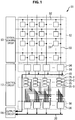
- FIG. 1 is a block diagram illustrating a configuration example of a first embodiment of an image sensor to which the present technology is applied.
- an image sensor 11 includes a pixel array unit 12, a vertical scanning circuit 13, a column-parallel analog-to-digital (AD) conversion unit 14, a column-parallel memory unit 15, a column-parallel inter-pixel image processing unit 16, a control circuit 17, and an output circuit 18.
- the image sensor 11 is a complementary metal oxide semiconductor (CMOS) image sensor.
- CMOS complementary metal oxide semiconductor
- the image sensor 11 can perform inter-pixel image processing between a certain pixel 31 and other four pixels 31 adjacent in a vertical direction and a horizontal direction with respect to the pixel 31.
- the pixel array unit 12 is a light-receiving surface that receives light collected by an optical system (not illustrated).
- a plurality of pixels 31 is two-dimensionally arranged in a matrix; the pixels 31 are connected to the vertical scanning circuit 13 via a row control line 32 for each row, and are connected to the column-parallel AD conversion unit 14 via a column signal line 33 for each column.
- Each of the plurality of pixels 31 has a photoelectric conversion function and outputs a pixel signal of a level corresponding to an amount of received light; an image of a subject formed on the pixel array unit 12 is constructed from the image signals.
- the vertical scanning circuit 13 supplies various driving signals for driving the pixels 31 to the pixels 31 via the row control lines 32, sequentially for each row of the plurality of pixels 31 arranged in the pixel array unit 12, to control reading of pixel signals for each row of the pixels 31.
- the column-parallel AD conversion unit 14 performs correlated double sampling (CDS) processing on pixel signals output from the plurality of pixels 31 via the column signal lines 33, thereby performing AD conversion on the pixel signals and reducing reset noise. That is, the column-parallel AD conversion unit 14 includes a plurality of AD conversion units 34 arranged in accordance with the number of columns of the pixels 31, and outputs digital signals obtained by performing AD conversion on pixel signals in parallel in the respective AD conversion units 34. In addition, pixel signals output from the column-parallel AD conversion unit 14 are supplied to the column-parallel memory unit 15, and supplied to the output circuit 18 via a bus 19.
- CDS correlated double sampling
- the column-parallel AD conversion unit 14 can apply a configuration based on a slope-type AD conversion circuit, because grayscale variability in AD conversion can be achieved easily by controlling a current source.
- the column-parallel AD conversion unit 14, in accordance with control by the control circuit 17, can select grayscale variability in performing AD conversion on pixel signals output from the pixels 31 to be an appropriate grayscale corresponding to contents of image processing.
- the image sensor 11 can achieve further high-speed image processing. Specifically, in the image sensor 11, AD conversion is performed with 12 bits in normal imaging, but performed with 4 bits in image processing; thus, slope-type AD conversion time is 1/256, and AD conversion time can be significantly shortened.
- the column-parallel memory unit 15 holds digital pixel signals of any number of rows output from the column-parallel AD conversion unit 14.
- the column-parallel memory unit 15 includes memory circuits 35 that are each capable of holding a pixel signal of one pixel and are arranged for each column of the pixels 31, the number of the memory circuits 35 corresponding to any number of rows.
- the column-parallel memory unit 15 includes three rows of memory circuits 35-1 to 35-3 for each column of the pixels 31.
- the column-parallel inter-pixel image processing unit 16 can perform any column-parallel inter-pixel computing in parallel.
- the column-parallel inter-pixel image processing unit 16 includes a plurality of inter-pixel image processing circuits 36 arranged in accordance with the number of columns of the pixels 31, and the column-parallel inter-pixel image processing unit 16 is connected to any plurality of rows and columns of memory circuits 35 of the column-parallel memory unit 15. Therefore, the column-parallel inter-pixel image processing unit 16 can perform image processing between any plurality of rows and columns of pixels 31 by the inter-pixel image processing circuits 36 for each column of the pixels 31 performing inter-pixel image processing in parallel.
- the column-parallel inter-pixel image processing unit 16 to the column-parallel inter-pixel image processing unit 16 are connected memory circuits 35-1 to 35-3 of the column in which itself is disposed and two memory circuits 35-2 arranged in the left and right columns thereof. Then, the column-parallel inter-pixel image processing unit 16 can perform inter-pixel image processing between the memory circuit 35-2 of the column in which itself is disposed and the other four memory circuits 35 adjacent in the vertical direction and the horizontal direction with respect to the memory circuit 35-2.
- pixel signals subjected to inter-pixel image processing in the column-parallel inter-pixel image processing unit 16 are supplied to the output circuit 18 via a bus 20.
- the control circuit 17 controls the pixel array unit 12, the column-parallel AD conversion unit 14, the column-parallel memory unit 15, and the column-parallel inter-pixel image processing unit 16.
- the output circuit 18 controls output, to the outside of a chip, of pixel signals supplied from the column-parallel AD conversion unit 14 via the bus 19 and pixel signals supplied from the column-parallel inter-pixel image processing unit 16 via the bus 20.
- the output circuit 18 can, in coordination with the vertical scanning circuit 13 and the control circuit 17, freely control pixel signals supplied from the column-parallel AD conversion unit 14 and pixel signals supplied from the column-parallel inter-pixel image processing unit 16, such as simultaneously outputting them, individually outputting them, or alternately outputting them.
- the image sensor 11 is configured as described above, can cause the column-parallel AD conversion unit 14 and the column-parallel inter-pixel image processing unit 16 to operate in parallel, and can achieve inter-pixel image processing with high speed and low latency.
- the column-parallel memory unit 15 includes three rows of memory circuits 35-1 to 35-3 for each column of the pixels 31, each being connected to the inter-pixel image processing circuits 36 in a necessary range.
- the image sensor 11 can increase the number of rows of the memory circuits 35 and connections with the inter-pixel image processing circuits 36.
- the image sensor 11 can achieve inter-pixel image processing with appropriate memory size and connection configuration as necessary.
- the memory circuits 35 have flexibility in a column direction as well as the number of rows, and for example, can achieve inter-pixel image processing in a wide range without increasing connections with the inter-pixel image processing circuits 36, by thinning out columns.
- it can be achieved by freely thinning out or adding reading of the pixels 31 itself, instead of increasing the memory circuits 35.
- a general-purpose memory such as a static random access memory (SRAM) or a dynamic random access memory (DRAM) can be used as the memory circuit 35, but a flip-flop circuit that is easy to control can also be used, because column-parallel input/output control is necessary.
- SRAM static random access memory
- DRAM dynamic random access memory
- FIG. 2 illustrates an operation timing chart of the image sensor 11.
- the image sensor 11 can cause pixel reading processing of reading pixel signals from the pixel array unit 12 out to the column-parallel AD conversion unit 14, AD conversion processing on pixel signals performed by the column-parallel AD conversion unit 14, data output processing of outputting data from the column-parallel AD conversion unit 14 and the column-parallel inter-pixel image processing unit 16, and inter-pixel image processing performed by the column-parallel inter-pixel image processing unit 16 to operate in parallel.
- the image sensor 11 can achieve high-speed imaging by pixel reading processing, AD conversion processing, data output processing, and inter-pixel image processing being executed to operate in parallel in accordance with control by the control circuit 17.
- the image sensor 11 can cause the column-parallel AD conversion unit 14 and the column-parallel inter-pixel image processing unit 16 to operate in parallel via the column-parallel memory unit 15.
- the image sensor 11 can execute inter-pixel image processing performed by the column-parallel inter-pixel image processing unit 16, while keeping high processing speed substantially the same as that of AD conversion processing performed by the column-parallel AD conversion unit 14. That is, the image sensor 11 can achieve inter-pixel image processing with high speed and low latency, whose latency is extremely low to the extent of row processing time that enables the column-parallel inter-pixel image processing unit 16 to operate in parallel with AD conversion processing performed by the column-parallel AD conversion unit 14.
- the image sensor 11 can have a function equivalent to that of a conventional imaging device including the column-parallel AD conversion unit 14, by putting the column-parallel inter-pixel image processing unit 16 on standby or interrupting power supply to it.
- actual operation speed of the image sensor 11 depends on parallel pieces of processing that operate in parallel. For example, in the case where each piece of processing is performed with 4 bits in the image sensor 11, also settling time dominating pixel reading processing of reading pixel signals from the pixel array unit 12 can be significantly shortened by being defined by precision of 4 bits. That is, in this case, necessary time precision can be relaxed as much as 256 times. Similarly, data output processing of outputting data from the output circuit 18 becomes 1/256 by data amount being reduced to 4 bits, and inter-pixel image processing performed by the column-parallel inter-pixel image processing unit 16 becomes 1/3 by computing in units of bits becoming 4 bits. Thus, the image sensor 11 can shorten parallel processing time in all pieces of processing, thereby achieving sensor operation and image processing at higher speed.
- the image sensor 11 can reduce the circuit size of the memory circuit 35 and the inter-pixel image processing circuit 36 by reducing gray levels in image processing.
- FIG. 3 is a block diagram illustrating a configuration example of the inter-pixel image processing circuit 36 in FIG. 1 .
- the inter-pixel image processing circuit 36 includes a bit selection circuit unit 41, a pixel selection circuit unit 42, a computing selection circuit unit 43, a computing unit 44, a carry control unit 45, an output circuit unit 46, a working memory unit 47, a working memory internal selection circuit 48, and a working memory external selection circuit 49.
- the bit selection circuit unit 41 selects any bit of a plurality of pixel signals.
- the bit selection circuit unit 41 includes five selectors 51-1 to 51-5.
- the bit selection circuit unit 41 selects any bit of pixel signals held in the connected memory circuits 35 by the five selectors 51-1 to 51-5.
- the pixel selection circuit unit 42 selects any pixel signal.
- the pixel selection circuit unit 42 includes two selectors 52-1 and 52-2.
- the selector 52-1 selects any pixel signal from among five pixel signals supplied via the bit selection circuit unit 41 and outputs the pixel signal, for example.
- the selector 52-2 selects a pixel signal to be subjected to computing with the pixel signal selected by the selector 52-1 and outputs the pixel signal, for example.
- the computing selection circuit unit 43 selects a pixel signal to be supplied to the computing unit 44 from among a pixel signal input from the pixel selection circuit unit 42, a pixel signal input from the working memory internal selection circuit 48, a pixel signal input from another inter-pixel image processing circuit 36 (not illustrated), and a pixel signal directly input from the outside.
- the computing selection circuit unit 43 includes two selectors 53-1 and 53-2.
- the selector 53-1 selects one of a pixel signal selected by the selector 52-1 of the pixel selection circuit unit 42, a pixel signal selected by a selector 54-1 of the working memory internal selection circuit 48, a pixel signal input from another inter-pixel image processing circuit 36 (not illustrated), and a pixel signal directly input from the outside, and supplies the pixel signal to the computing unit 44.
- the selector 53-2 selects one of a pixel signal selected by the selector 52-2 of the pixel selection circuit unit 42, a pixel signal selected by a selector 54-2 of the working memory internal selection circuit 48, a pixel signal input from another inter-pixel image processing circuit 36 (not illustrated), and a pixel signal directly input from the outside, and supplies the pixel signal to the computing unit 44.
- the computing unit 44 performs computing between pixel signals by using two pixel signals supplied from the computing selection circuit unit 43, and performs output.
- the carry control unit 45 performs carry control when the computing unit 44 performs computing.
- the output circuit unit 46 temporarily holds a pixel signal output from the computing unit 44, thereby enabling computing and output to operate in parallel.
- the working memory unit 47 temporarily holds a pixel signal output from the computing unit 44 so that the pixel signal can be used when computing using the pixel signal is performed again.
- the working memory internal selection circuit 48 selects and outputs a pixel signal held in the working memory unit 47 for computing inside the inter-pixel image processing circuit 36.
- the working memory internal selection circuit 48 includes the two selectors 54-1 and 54-2.
- the selector 54-1 supplies the selected pixel signal to the selector 53-1 of the computing selection circuit unit 43
- the selector 54-2 supplies the selected pixel signal to the selector 53-2 of the computing selection circuit unit 43.
- the working memory external selection circuit 49 selects and outputs a pixel signal held in the working memory unit 47 for computing with another inter-pixel image processing circuit 36 (not illustrated).
- the working memory external selection circuit 49 includes two selectors 55-1 and 55-2.
- the selector 55-1 supplies the selected pixel signal to the selector 53-1 of the computing selection circuit unit 43 of the other inter-pixel image processing circuit 36 (not illustrated), and the selector 54-2 supplies the selected pixel signal to the selector 53-2 of the computing selection circuit unit 43 of the other inter-pixel image processing circuit 36 (not illustrated).
- the column-parallel inter-pixel image processing unit 16 includes the plurality of inter-pixel image processing circuits 36 configured as described above, and with the connection configuration with the column-parallel memory unit 15, can perform any one-dimensional or two-dimensional inter-pixel image processing.
- the column-parallel inter-pixel image processing unit 16 can perform any convolution operation processing, such as smoothing or edge extraction, and feature value extraction, such as corner extraction.
- the image sensor 11 in the configuration example illustrated in FIG. 1 premises performing inter-pixel image processing using a certain pixel 31 and other four pixels 31 adjacent in the vertical direction and the horizontal direction with respect to the pixel 31. Therefore, the bit selection circuit unit 41 has a configuration including five selectors 51-1 to 51-5, but the number of selectors 51 included in the bit selection circuit unit 41 can be increased so as to correspond to the column-parallel AD conversion unit 14 as necessary. Thus, the image sensor 11 can perform image processing between neighboring pixels in a wider range.
- the computing unit 44 can have a simple basic configuration including an adder and a logical operation circuit, because it performs bit serial 2-input computing.
- the computing unit 44 can have a single instruction/multiple data (SIMD)-type parallel computing function suitable for high-speed parallel processing.
- SIMD single instruction/multiple data
- the image sensor 11 can alternately perform output of images at a normal speed of 120 frames per second (fps) and output of images at a high speed of 960 fps. That is, the output circuit 18 alternately performs output control for outputting pixel signals output from the column-parallel AD conversion unit 14 at 120 fps and output control for outputting pixel signals output from the column-parallel inter-pixel image processing unit 16 at 960 fps.
- the image sensor 11 can output images subjected to high-speed image processing at 960 fps in the background, while continuously outputting normal images corresponding to 60 fps.
- the output circuit 18 can perform integral or statistical processing, such as moment computing or histogram processing, for example, at any time by using all or part of outputs of the column-parallel AD conversion unit 14 and the column-parallel inter-pixel image processing unit 16. Then, the image sensor 11 can output pixel signals subjected to the processing.
- the image sensor 11 can cause output of the column-parallel AD conversion unit 14 and output of the column-parallel inter-pixel image processing unit 16 to be performed in parallel by having a configuration in which the column-parallel AD conversion unit 14 and the column-parallel memory unit 15 are provided to precede the column-parallel inter-pixel image processing unit 16.
- the image sensor 11 can achieve inter-pixel image processing with low latency and high speed, which has been impossible in conventional column-parallel image processing, while keeping an advantage that no constraints are placed on the pixel array unit 12 and the column-parallel AD conversion unit 14.
- FIG. 5 is a block diagram illustrating a second configuration example of an image sensor. Note that in an image sensor 11A illustrated in FIG. 5 , components common to the image sensor 11 in FIG. 1 are denoted by the same reference numerals, and detailed description thereof is omitted.
- the image sensor 11A is similar to the image sensor 11 in FIG. 1 in that the pixel array unit 12, the vertical scanning circuit 13, the column-parallel AD conversion unit 14, the column-parallel memory unit 15, the column-parallel inter-pixel image processing unit 16, the control circuit 17, and the output circuit 18 are provided.
- the image sensor 11A further includes a column-parallel grayscale conversion unit 21, a frame memory unit 22, and a column-parallel inter-frame image processing unit 23.
- the column-parallel grayscale conversion unit 21 can perform grayscale conversion processing based on any threshold, in parallel for each column, on pixel signals subjected to column-parallel inter-pixel image processing in the column-parallel inter-pixel image processing unit 16. That is, the column-parallel grayscale conversion unit 21 includes a plurality of grayscale conversion circuits 37 arranged in accordance with the number of columns of the pixels 31, and the grayscale conversion circuit 37 performs grayscale conversion on a pixel signal output from the inter-pixel image processing circuit 36 of the corresponding column, and outputs the resulting pixel signal.
- the column-parallel grayscale conversion unit 21, in accordance with control by the control circuit 17, can change a grayscale when a grayscale of a pixel signal is changed.
- a variable range in which the column-parallel AD conversion unit 14 changes a grayscale is set to be equal to or greater than a variable range in which the column-parallel grayscale conversion unit 21 changes a grayscale.
- the frame memory unit 22 holds one frame of pixel signals subjected to grayscale conversion and output by the column-parallel grayscale conversion unit 21.
- the column-parallel inter-frame image processing unit 23 performs inter-frame image processing by using an image based on pixel signals output from the column-parallel grayscale conversion unit 21 and an image based on pixel signals of the immediately preceding frame held in the frame memory unit 22. That is, the column-parallel inter-frame image processing unit 23 includes a plurality of inter-frame image processing circuits 38 arranged in accordance with the number of columns of the pixels 31, and the inter-frame image processing circuits 38 perform signal processing between an image of the current frame and an image of the immediately preceding frame in a column-parallel manner. By performing such inter-frame image processing, the column-parallel inter-frame image processing unit 23 can, for example, detect a motion of a subject between frames.
- the control circuit 17 can cause pixel reading processing, AD conversion processing, data output processing, and inter-pixel image processing to operate in parallel, and also can cause inter-frame image processing performed by the column-parallel inter-frame image processing unit 23 to operate in parallel. That is, the image sensor 11A can cause inter-frame image processing performed by the column-parallel inter-frame image processing unit 23 to operate in parallel with AD conversion processing of the column-parallel AD conversion unit 14 ( FIG. 2 ) via the frame memory unit 22. Thus, the image sensor 11A can perform inter-pixel image processing and inter-frame image processing with high speed and low delay.
- the image sensor 11A can perform inter-frame image processing by the column-parallel inter-frame image processing unit 23 by using an image subjected to appropriate pre-filtering processing such as denoising by the column-parallel inter-pixel image processing unit 16.
- appropriate pre-filtering processing such as denoising by the column-parallel inter-pixel image processing unit 16.
- the image sensor 11A can be treated as being equivalent to a conventional imaging device by putting the column-parallel inter-frame image processing unit 23 on standby or interrupting power supply to it, in the case where inter-frame image processing by the column-parallel inter-frame image processing unit 23 is unnecessary.
- the column-parallel grayscale conversion unit 21 reduces gray levels to a range necessary in inter-frame image processing of the column-parallel inter-frame image processing unit 23.
- the column-parallel inter-frame image processing unit 23 performs inter-frame image processing by using pixel signals with reduced gray levels of the immediately preceding frame held in the frame memory unit 22 and pixel signals with reduced gray levels of the current frame. By such processing, the image sensor 11A can achieve inter-frame image processing with the frame memory unit 22 having a configuration of minimum capacity.
- the frame memory unit 22 it is also possible for the frame memory unit 22 to include a flip-flop circuit.
- the frame memory unit 22 has larger capacity than the column-parallel memory unit 15 of the image sensor 11 in FIG. 1 , and therefore preferably includes a general-purpose memory such as a SRAM or a DRAM.
- the frame memory unit 22 it is practical for the frame memory unit 22 to include a flip-flop circuit of minimum capacity necessary for temporary work in column-parallel processing.
- the inter-frame image processing circuit 38 can employ a configuration similar to that of the inter-pixel image processing circuit 36 described with reference to FIG. 3 . Note that in the case where the inter-frame image processing circuit 38 is specialized for simple processing, such as detecting whether or not there is a motion of a subject between frames, a simple configuration based on a logical operation circuit can be used.
- the column-parallel inter-frame image processing unit 23 is connected to the output circuit 18 via a bus 24. Therefore, for example, the output circuit 18 can, in coordination with the vertical scanning circuit 13 and the control circuit 17, freely control pixel signals supplied from the column-parallel AD conversion unit 14, pixel signals supplied from the column-parallel inter-pixel image processing unit 16, and pixel signals output from the column-parallel inter-frame image processing unit 23, such as simultaneously outputting them, individually outputting them, or alternately outputting them.
- the image sensor 11A has a configuration in which, in addition to the configuration of the image sensor 11 in FIG. 1 , the column-parallel grayscale conversion unit 21, the frame memory unit 22, and the column-parallel inter-frame image processing unit 23 are provided to follow the column-parallel inter-pixel image processing unit 16.
- the image sensor 11A can achieve inter-frame image processing with high speed and low delay, in addition to inter-pixel image processing, with a minimum amount of memory.
- the image sensor 11A can, while enabling normal imaging, achieve further high-speed column-parallel image processing when gray levels are reduced.
- FIG. 6 is a block diagram illustrating a third configuration example of an image sensor. Note that in an image sensor 11B illustrated in FIG. 6 , components common to the image sensor 11 in FIG. 1 are denoted by the same reference numerals, and detailed description thereof is omitted.
- the image sensor 11B is similar to the image sensor 11 in FIG. 1 in that the pixel array unit 12, the vertical scanning circuit 13, the column-parallel memory unit 15, the column-parallel inter-pixel image processing unit 16, the control circuit 17, and the output circuit 18 are provided.
- the image sensor 11B has a configuration in which a column-parallel AD conversion unit 14-1 is disposed below the pixel array unit 12 in the vertical direction and a column-parallel AD conversion unit 14-2 is disposed above the pixel array unit 12 in the vertical direction. Then, in the image sensor 11B, for example, pixels 31 of odd-numbered rows of the pixel array unit 12 are connected to the column-parallel AD conversion unit 14-1 via column signal lines 33-1, and pixels 31 of even-numbered rows of the pixel array unit 12 are connected to the column-parallel AD conversion unit 14-2 via column signal lines 33-2.
- the column-parallel AD conversion unit 14-1 includes AD conversion units 34-1, the number of which corresponds to the pixels 31 of the odd-numbered rows of the pixel array unit 12, and supplies digital signals obtained by performing AD conversion on pixel signals in parallel in the respective AD conversion units 34-1 to the output circuit 18 via the bus 19.
- the column-parallel AD conversion unit 14-2 includes AD conversion units 34-2, the number of which corresponds to the pixels 31 of the even-numbered rows of the pixel array unit 12, and supplies digital signals obtained by performing AD conversion on pixel signals in parallel in the respective AD conversion units 34-2 to the output circuit 18 via a bus 25.
- the column-parallel AD conversion unit 14-1 and the column-parallel AD conversion unit 14-2 preferably have equivalent performance.
- the column-parallel AD conversion unit 14-1 performs AD conversion on pixel signals of one row with a second grayscale smaller than the first grayscale.
- the image sensor 11B has a configuration in which the column-parallel AD conversion unit 14-1 and the column-parallel AD conversion unit 14-2 are arranged to face the pixel array unit 12.
- a configuration in which the column-parallel AD conversion unit 14-1 and the column-parallel AD conversion unit 14-2 are arranged on the same side with respect to the pixel array unit 12 may be used, in which case routing of the bus 25 can be shortened.
- the output circuit 18 can perform integral or statistical processing, such as moment computing or histogram processing, for example, at any time by using all or part of outputs of the column-parallel AD conversion units 14-1 and 14-2 and the column-parallel inter-pixel image processing unit 16. Then, the image sensor 11B can output pixel signals subjected to the processing.
- the control circuit 17 can cause pixel reading processing, AD conversion processing performed by the column-parallel AD conversion units 14-1 and 14-2, data output processing, and inter-pixel image processing to operate in parallel.
- the output circuit 18 can, in coordination with the vertical scanning circuit 13 and the control circuit 17, freely control pixel signals supplied from the column-parallel AD conversion units 14-1 and 14-2, pixel signals supplied from the column-parallel inter-pixel image processing unit 16, and pixel signals output from the column-parallel inter-frame image processing unit 23, such as simultaneously outputting them, individually outputting them, or alternately outputting them.
- the image sensor 11B can perform output of images at a normal speed of 60 fps and output of images at a high speed of 960 fps concurrently in parallel. That is, the output circuit 18 concurrently performs output control for outputting pixel signals output from the column-parallel AD conversion unit 14-2 at 60 fps and output control for outputting pixel signals output from the column-parallel inter-pixel image processing unit 16 via the column-parallel AD conversion unit 14-1 at 960 fps.
- the image sensor 11B can continuously output normal images corresponding to 60 fps.
- images subjected to high-speed image processing at 960 fps can be output concurrently in parallel with output of normal images corresponding to 60 fps.
- the image sensor 11B can have a configuration in which blocks equivalent to the column-parallel memory unit 15 and the column-parallel inter-pixel image processing unit 16 are arranged on the output side of the column-parallel AD conversion unit 14-2, as on the output side of the column-parallel AD conversion unit 14-1. Employing this configuration for the image sensor 11B can achieve further high-speed image processing, though a circuit area is increased.
- the image sensor 11B can achieve further high-speed image processing, though a circuit area and power consumption are traded off.
- FIG. 8 is a block diagram illustrating a fourth configuration example of an image sensor. Note that in an image sensor 11C illustrated in FIG. 8 , components common to the image sensor 11A in FIG. 5 and the image sensor 11B in FIG. 6 are denoted by the same reference numerals, and detailed description thereof is omitted.
- the image sensor 11C has the configurations of the image sensor 11A in FIG. 5 and the image sensor 11B in FIG. 6 .
- the image sensor 11C includes the pixel array unit 12, the vertical scanning circuit 13, the column-parallel AD conversion units 14-1 and 14-2, the column-parallel memory unit 15, the column-parallel inter-pixel image processing unit 16, the control circuit 17, the output circuit 18, the column-parallel grayscale conversion unit 21, the frame memory unit 22, and the column-parallel inter-frame image processing unit 23.
- the image sensor 11C configured as described above can execute inter-frame image processing in a column-parallel manner, like the image sensor 1 1A in FIG. 5 , and also can perform output of images at a normal speed of 60 fps and output of images at a high speed of 960 fps concurrently in parallel, like the image sensor 11B in FIG. 6 .
- FIG. 9 is a block diagram illustrating a fifth configuration example of an image sensor. Note that in an image sensor 11D illustrated in FIG. 9 , components common to the image sensor 11C in FIG. 8 are denoted by the same reference numerals, and detailed description thereof is omitted.
- the image sensor 11D includes the pixel array unit 12, the vertical scanning circuit 13, the column-parallel AD conversion units 14-1 and 14-2, the column-parallel memory unit 15, the column-parallel inter-pixel image processing unit 16, the control circuit 17, the output circuit 18, the column-parallel grayscale conversion unit 21, the frame memory unit 22, and the column-parallel inter-frame image processing unit 23.
- the image sensor 11D has a stacked structure in which two layers of a semiconductor chip 61-1 and a semiconductor chip 61-2 are stacked, and wiring between the semiconductor chip 61-1 and the semiconductor chip 61-2 is joined by a connection portion 62.
- the semiconductor chip 61-1 are arranged the pixel array unit 12, the vertical scanning circuit 13, and the column-parallel AD conversion units 14-1 and 14-2.
- the column-parallel memory unit 15 are arranged on the column-parallel inter-pixel image processing unit 16, the control circuit 17, the output circuit 18, the column-parallel grayscale conversion unit 21, the frame memory unit 22, and the column-parallel inter-frame image processing unit 23.
- the image sensor 11D configured as described above has an arrangement forming a stacked structure in which a column-parallel circuit portion (the column-parallel memory unit 15, the column-parallel inter-pixel image processing unit 16, the control circuit 17, the output circuit 18, the column-parallel grayscale conversion unit 21, the frame memory unit 22, the column-parallel inter-frame image processing unit 23, and the like) is folded back against the pixel array unit 12.
- a column-parallel circuit portion the column-parallel memory unit 15, the column-parallel inter-pixel image processing unit 16, the control circuit 17, the output circuit 18, the column-parallel grayscale conversion unit 21, the frame memory unit 22, the column-parallel inter-frame image processing unit 23, and the like
- the image sensor 11D has a configuration in which the column-parallel circuit portion is collected on the semiconductor chip 61-2, separately from the semiconductor chip 61-1 including the pixel array unit 12.
- the image sensor 11D can use a leading-edge logic process independent of pixel and analog techniques in the semiconductor chip 61-2, which is advantageous in area efficiency and routing of signal lines.
- the image sensor 11D has a configuration in which outputs of the column-parallel AD conversion units 14-1 and 14-2 are connected to the semiconductor chip 61-2.
- a configuration in which another output is connected to the semiconductor chip 61-2 can be used, in accordance with area balance between the semiconductor chip 61-1 and the semiconductor chip 61-2 or a chip process.
- other circuit arrangements of the image sensor 11D are also not limited to the configuration example in FIG. 9 .
- connection portion 62 can employ various methods such as a bump joint using a solder technique or a substrate-penetrating electrode to which a semiconductor process is applied, for example, and is not limited to a specific method.
- the image sensor 11D is not limited to a stacked structure of two chips of the semiconductor chip 61-1 and the semiconductor chip 61-2.
- a stacked structure of three chips can be employed in which a process chip suitable for a large-capacity memory such as a DRAM is sandwiched between the semiconductor chip 61-1 and the semiconductor chip 61-2. That is, the image sensor 11D can have a configuration in which the column-parallel memory unit 15, the column-parallel inter-pixel image processing unit 16, the control circuit 17, the output circuit 18, the column-parallel grayscale conversion unit 21, and the column-parallel inter-frame image processing unit 23 are arranged on the third layer of semiconductor chip.
- image sensor 11 can be applied to, for example, various electronic apparatuses, such as imaging systems (e.g., digital still cameras and digital video cameras), mobile phones with an imaging function, or other apparatuses with an imaging function.
- imaging systems e.g., digital still cameras and digital video cameras
- mobile phones with an imaging function e.g., mobile phones with an imaging function
- other apparatuses with an imaging function e.g., mobile phones with an imaging function
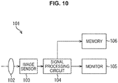
- FIG. 10 is a block diagram illustrating a configuration example of an imaging device mounted on an electronic apparatus.
- an imaging device 101 includes an optical system 102, an image sensor 103, a signal processing circuit 104, a monitor 105, and a memory 106, and can capture still images and moving images.
- the optical system 102 includes one or a plurality of lenses, and guides image light (incident light) from a subject to the image sensor 103 to form an image on a light-receiving surface (pixel array unit) of the image sensor 103.
- the above-described image sensor 11 is used as the image sensor 103. Electrons are accumulated in the image sensor 103 for a certain period, in accordance with the image formed on the light-receiving surface through the optical system 102. Then, signals corresponding to the electrons accumulated in the image sensor 103 are supplied to the signal processing circuit 104.
- the signal processing circuit 104 performs various kinds of signal processing on pixel signals output from the image sensor 103.
- An image (image data) obtained by the signal processing circuit 104 performing signal processing is supplied to the monitor 105 to be displayed, or supplied to the memory 106 to be stored (recorded).
- an image subjected to inter-pixel image processing with lower latency and higher speed can be captured, for example, by using the above-described image sensor 11.
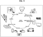
- FIG. 11 illustrates the usage examples of the above-described image sensor (the image sensor 11).
- the above-described image sensor can be used for, for example, various cases in which light such as visible light, infrared light, ultraviolet light, or X-rays is detected as follows.
- present technology may also be configured as below.
Landscapes
- Engineering & Computer Science (AREA)
- Multimedia (AREA)
- Signal Processing (AREA)
- Physics & Mathematics (AREA)
- General Physics & Mathematics (AREA)
- Theoretical Computer Science (AREA)
- Transforming Light Signals Into Electric Signals (AREA)
- Image Processing (AREA)
Abstract
Description
- The present disclosure relates to an image sensor and a driving method, and an electronic apparatus, and particularly relates to an image sensor and a driving method, and an electronic apparatus that are capable of performing inter-pixel image processing with lower latency and higher speed.
- Conventionally, for the purpose of performing processing such as authentication and recognition with higher speed and low latency, a vision chip obtained by integrating an imaging portion and an image processing portion of an image sensor onto a chip has been under research.
- For example, an imaging device has been known in which, in regard to a plurality of pixels two-dimensionally arranged in a matrix and having a photoelectric conversion function, one image processing circuit is disposed for one pixel, and image processing is performed in parallel. In this imaging device, image processing can be performed with higher speed and low latency. However, an image processing circuit generally occupies a larger area than a pixel size, which makes it difficult to make a pixel portion for photoelectric conversion large; thus, it has been difficult to obtain sufficient sensitivity characteristics. In addition, an area of one unit pixel including an image processing circuit and a pixel is large, which makes it difficult to increase the number of pixels.
- Hence,
Patent Literature 1 discloses large-scale integration (LSI) for pattern signal processing that employs a configuration in which one processor element is made to correspond to one column of sensors. Employing this configuration can, for example, reduce the number of image processing circuits necessary for pixels, and relax limitations on the pixel size and the number of pixels as described above. - Patent Literature 1:
JP H7-62866B - Incidentally, the technology disclosed in
Patent Literature 1 described above has a configuration in which signal processing is performed by directly selecting pixel outputs by a multiplexer. Therefore, in this configuration, each time signal processing is performed, signal processing of one row is repeated after pixel outputs necessary for processing are scanned and selected; hence, image processing takes time, which makes it difficult to increase the speed of processing. - The present disclosure has been made in view of such circumstances, and makes it possible to perform inter-pixel image processing with lower latency and higher speed.
- An image sensor according to an aspect of the present disclosure includes: a pixel array unit in which pixels having a photoelectric conversion function are arranged in an array; an AD conversion unit configured to perform analog-to-digital (AD) conversion processing on pixel signals output from the pixels in parallel for each column of the pixels of the pixel array unit; a memory unit configured to hold pixel signals of any number of rows subjected to AD conversion in the AD conversion unit for each column of the pixels; an inter-pixel image processing unit configured to read pixel signals of any rows and columns from the memory unit, and perform computing between the pixel signals in parallel for each column of the pixels; and an output circuit configured to control output, to an outside, of pixel signals output from the AD conversion unit and pixel signals output from the inter-pixel image processing unit.
- A driving method according to an aspect of the present disclosure is a method for driving an image sensor including a pixel array unit in which pixels having a photoelectric conversion function are arranged in an array, an AD conversion unit configured to perform AD conversion processing on pixel signals output from the pixels in parallel for each column of the pixels of the pixel array unit, a memory unit configured to hold pixel signals of any number of rows subjected to AD conversion in the AD conversion unit for each column of the pixels, an inter-pixel image processing unit configured to read pixel signals of any rows and columns from the memory unit, and perform computing between the pixel signals in parallel for each column of the pixels, and an output circuit configured to control output, to an outside, of pixel signals output from the AD conversion unit and pixel signals output from the inter-pixel image processing unit, the method including: causing pixel reading processing of reading pixel signals from the pixel array unit out to the AD conversion unit, AD conversion processing on pixel signals performed by the AD conversion unit, inter-pixel image processing performed by the inter-pixel image processing unit, and data output processing of outputting data from the AD conversion unit and the inter-pixel image processing to operate in parallel.
- An electronic apparatus according to an aspect of the present disclosure includes an image sensor including a pixel array unit in which pixels having a photoelectric conversion function are arranged in an array, an AD conversion unit configured to perform AD conversion processing on pixel signals output from the pixels in parallel for each column of the pixels of the pixel array unit, a memory unit configured to hold pixel signals of any number of rows subjected to AD conversion in the AD conversion unit for each column of the pixels, an inter-pixel image processing unit configured to read pixel signals of any rows and columns from the memory unit, and perform computing between the pixel signals in parallel for each column of the pixels, and an output circuit configured to control output, to an outside, of pixel signals output from the AD conversion unit and pixel signals output from the inter-pixel image processing unit.
- In an aspect of the present disclosure, pixels having a photoelectric conversion function are arranged in an array in a pixel array unit. In an AD conversion unit, AD conversion processing on pixel signals output from the pixels is performed in parallel for each column of the pixels of the pixel array unit. In a memory unit, pixel signals of any number of rows subjected to AD conversion in the AD conversion unit are held for each column of the pixels. In an inter-pixel image processing unit, pixel signals of any rows and columns are read from the memory unit, and computing between the pixel signals is performed in parallel for each column of the pixels. In an output circuit, output, to an outside, of pixel signals output from the AD conversion unit and pixel signals output from the inter-pixel image processing unit is controlled.
- According to an aspect of the present disclosure, inter-pixel image processing can be performed with lower latency and higher speed.
-
-
FIG. 1 is a block diagram illustrating a configuration example of a first embodiment of an image sensor to which the present technology is applied. -
FIG. 2 illustrates an operation timing chart of an image sensor. -
FIG. 3 is a block diagram illustrating a configuration example of an inter-pixel image processing circuit. -
FIG. 4 illustrates an example of output control. -
FIG. 5 is a block diagram illustrating a configuration example of a second embodiment of an image sensor. -
FIG. 6 is a block diagram illustrating a configuration example of a third embodiment of an image sensor. -
FIG. 7 illustrates an example of output control. -
FIG. 8 is a block diagram illustrating a configuration example of a fourth embodiment of an image sensor. -
FIG. 9 is a block diagram illustrating a configuration example of a fifth embodiment of an image sensor. -
FIG. 10 is a block diagram illustrating a configuration example of an imaging device. -
FIG. 11 illustrates usage examples of an image sensor. - Hereinafter, specific embodiments to which the present technology is applied will be described in detail with reference to the drawings.
-
FIG. 1 is a block diagram illustrating a configuration example of a first embodiment of an image sensor to which the present technology is applied. - As illustrated in
FIG. 1 , animage sensor 11 includes apixel array unit 12, avertical scanning circuit 13, a column-parallel analog-to-digital (AD)conversion unit 14, a column-parallel memory unit 15, a column-parallel inter-pixelimage processing unit 16, acontrol circuit 17, and anoutput circuit 18. For example, theimage sensor 11 is a complementary metal oxide semiconductor (CMOS) image sensor. In addition, in the configuration example illustrated inFIG. 1 , theimage sensor 11 can perform inter-pixel image processing between acertain pixel 31 and other fourpixels 31 adjacent in a vertical direction and a horizontal direction with respect to thepixel 31. - The
pixel array unit 12 is a light-receiving surface that receives light collected by an optical system (not illustrated).
In thepixel array unit 12, a plurality ofpixels 31 is two-dimensionally arranged in a matrix; thepixels 31 are connected to thevertical scanning circuit 13 via arow control line 32 for each row, and are connected to the column-parallelAD conversion unit 14 via acolumn signal line 33 for each column. Each of the plurality ofpixels 31 has a photoelectric conversion function and outputs a pixel signal of a level corresponding to an amount of received light; an image of a subject formed on thepixel array unit 12 is constructed from the image signals. - The
vertical scanning circuit 13 supplies various driving signals for driving thepixels 31 to thepixels 31 via therow control lines 32, sequentially for each row of the plurality ofpixels 31 arranged in thepixel array unit 12, to control reading of pixel signals for each row of thepixels 31. - The column-parallel
AD conversion unit 14 performs correlated double sampling (CDS) processing on pixel signals output from the plurality ofpixels 31 via thecolumn signal lines 33, thereby performing AD conversion on the pixel signals and reducing reset noise. That is, the column-parallelAD conversion unit 14 includes a plurality ofAD conversion units 34 arranged in accordance with the number of columns of thepixels 31, and outputs digital signals obtained by performing AD conversion on pixel signals in parallel in the respectiveAD conversion units 34. In addition, pixel signals output from the column-parallelAD conversion unit 14 are supplied to the column-parallel memory unit 15, and supplied to theoutput circuit 18 via abus 19. - Note that various circuit configurations can be applied to the column-parallel
AD conversion unit 14; for example, it is preferable to apply a configuration based on a slope-type AD conversion circuit, because grayscale variability in AD conversion can be achieved easily by controlling a current source. For example, the column-parallelAD conversion unit 14, in accordance with control by thecontrol circuit 17, can select grayscale variability in performing AD conversion on pixel signals output from thepixels 31 to be an appropriate grayscale corresponding to contents of image processing. For example, by reducing gray levels by the column-parallelAD conversion unit 14, theimage sensor 11 can achieve further high-speed image processing. Specifically, in theimage sensor 11, AD conversion is performed with 12 bits in normal imaging, but performed with 4 bits in image processing; thus, slope-type AD conversion time is 1/256, and AD conversion time can be significantly shortened. - The column-
parallel memory unit 15 holds digital pixel signals of any number of rows output from the column-parallelAD conversion unit 14. For example, the column-parallel memory unit 15 includes memory circuits 35 that are each capable of holding a pixel signal of one pixel and are arranged for each column of thepixels 31, the number of the memory circuits 35 corresponding to any number of rows. For example, in the case of a configuration in which theimage sensor 11 performs inter-pixel image processing between acertain pixel 31 and other fourpixels 31 adjacent in the vertical direction and the horizontal direction with respect to thepixel 31, as illustrated inFIG. 1 , the column-parallel memory unit 15 includes three rows of memory circuits 35-1 to 35-3 for each column of thepixels 31. - The column-parallel inter-pixel
image processing unit 16 can perform any column-parallel inter-pixel computing in parallel. For example, the column-parallel inter-pixelimage processing unit 16 includes a plurality of inter-pixelimage processing circuits 36 arranged in accordance with the number of columns of thepixels 31, and the column-parallel inter-pixelimage processing unit 16 is connected to any plurality of rows and columns of memory circuits 35 of the column-parallel memory unit 15. Therefore, the column-parallel inter-pixelimage processing unit 16 can perform image processing between any plurality of rows and columns ofpixels 31 by the inter-pixelimage processing circuits 36 for each column of thepixels 31 performing inter-pixel image processing in parallel. - For example, in the case of a configuration in which the
image sensor 11 performs inter-pixel image processing between acertain pixel 31 and other fourpixels 31 adjacent in the vertical direction and the horizontal direction with respect to thepixel 31, as illustrated inFIG. 1 , to the column-parallel inter-pixelimage processing unit 16 are connected memory circuits 35-1 to 35-3 of the column in which itself is disposed and two memory circuits 35-2 arranged in the left and right columns thereof. Then, the column-parallel inter-pixelimage processing unit 16 can perform inter-pixel image processing between the memory circuit 35-2 of the column in which itself is disposed and the other four memory circuits 35 adjacent in the vertical direction and the horizontal direction with respect to the memory circuit 35-2. In addition, pixel signals subjected to inter-pixel image processing in the column-parallel inter-pixelimage processing unit 16 are supplied to theoutput circuit 18 via abus 20. - The
control circuit 17 controls thepixel array unit 12, the column-parallelAD conversion unit 14, the column-parallel memory unit 15, and the column-parallel inter-pixelimage processing unit 16. - The
output circuit 18 controls output, to the outside of a chip, of pixel signals supplied from the column-parallelAD conversion unit 14 via thebus 19 and pixel signals supplied from the column-parallel inter-pixelimage processing unit 16 via thebus 20. For example, theoutput circuit 18 can, in coordination with thevertical scanning circuit 13 and thecontrol circuit 17, freely control pixel signals supplied from the column-parallelAD conversion unit 14 and pixel signals supplied from the column-parallel inter-pixelimage processing unit 16, such as simultaneously outputting them, individually outputting them, or alternately outputting them. - The
image sensor 11 is configured as described above, can cause the column-parallelAD conversion unit 14 and the column-parallel inter-pixelimage processing unit 16 to operate in parallel, and can achieve inter-pixel image processing with high speed and low latency. - Note that in the
image sensor 11 inFIG. 1 , the column-parallel memory unit 15 includes three rows of memory circuits 35-1 to 35-3 for each column of thepixels 31, each being connected to the inter-pixelimage processing circuits 36 in a necessary range. On the other hand, in the case where inter-pixel image processing in a wider range is necessary or the case where color filters are arranged in a Bayer array and image processing between pixels of the same color is necessary, theimage sensor 11 can increase the number of rows of the memory circuits 35 and connections with the inter-pixelimage processing circuits 36. Thus, theimage sensor 11 can achieve inter-pixel image processing with appropriate memory size and connection configuration as necessary. - In addition, in the
image sensor 11, the memory circuits 35 have flexibility in a column direction as well as the number of rows, and for example, can achieve inter-pixel image processing in a wide range without increasing connections with the inter-pixelimage processing circuits 36, by thinning out columns. In addition, in the case where merely processing between remote pixels is necessary, it can be achieved by freely thinning out or adding reading of thepixels 31 itself, instead of increasing the memory circuits 35. - Note that a general-purpose memory such as a static random access memory (SRAM) or a dynamic random access memory (DRAM) can be used as the memory circuit 35, but a flip-flop circuit that is easy to control can also be used, because column-parallel input/output control is necessary.
-
FIG. 2 illustrates an operation timing chart of theimage sensor 11. - As illustrated in
FIG. 2 , theimage sensor 11 can cause pixel reading processing of reading pixel signals from thepixel array unit 12 out to the column-parallelAD conversion unit 14, AD conversion processing on pixel signals performed by the column-parallelAD conversion unit 14, data output processing of outputting data from the column-parallelAD conversion unit 14 and the column-parallel inter-pixelimage processing unit 16, and inter-pixel image processing performed by the column-parallel inter-pixelimage processing unit 16 to operate in parallel. Thus, theimage sensor 11 can achieve high-speed imaging by pixel reading processing, AD conversion processing, data output processing, and inter-pixel image processing being executed to operate in parallel in accordance with control by thecontrol circuit 17. - That is, the
image sensor 11 can cause the column-parallelAD conversion unit 14 and the column-parallel inter-pixelimage processing unit 16 to operate in parallel via the column-parallel memory unit 15. Thus, theimage sensor 11 can execute inter-pixel image processing performed by the column-parallel inter-pixelimage processing unit 16, while keeping high processing speed substantially the same as that of AD conversion processing performed by the column-parallelAD conversion unit 14. That is, theimage sensor 11 can achieve inter-pixel image processing with high speed and low latency, whose latency is extremely low to the extent of row processing time that enables the column-parallel inter-pixelimage processing unit 16 to operate in parallel with AD conversion processing performed by the column-parallelAD conversion unit 14. - Note that in the case where inter-pixel image processing by the column-parallel inter-pixel
image processing unit 16 is unnecessary, theimage sensor 11 can have a function equivalent to that of a conventional imaging device including the column-parallelAD conversion unit 14, by putting the column-parallel inter-pixelimage processing unit 16 on standby or interrupting power supply to it. - In addition, as illustrated in the timing chart in
FIG. 2 , actual operation speed of theimage sensor 11 depends on parallel pieces of processing that operate in parallel. For example, in the case where each piece of processing is performed with 4 bits in theimage sensor 11, also settling time dominating pixel reading processing of reading pixel signals from thepixel array unit 12 can be significantly shortened by being defined by precision of 4 bits. That is, in this case, necessary time precision can be relaxed as much as 256 times. Similarly, data output processing of outputting data from theoutput circuit 18 becomes 1/256 by data amount being reduced to 4 bits, and inter-pixel image processing performed by the column-parallel inter-pixelimage processing unit 16 becomes 1/3 by computing in units of bits becoming 4 bits. Thus, theimage sensor 11 can shorten parallel processing time in all pieces of processing, thereby achieving sensor operation and image processing at higher speed. - Furthermore, the
image sensor 11 can reduce the circuit size of the memory circuit 35 and the inter-pixelimage processing circuit 36 by reducing gray levels in image processing. -
FIG. 3 is a block diagram illustrating a configuration example of the inter-pixelimage processing circuit 36 inFIG. 1 . - As illustrated in
FIG. 3 , the inter-pixelimage processing circuit 36 includes a bit selection circuit unit 41, a pixelselection circuit unit 42, a computingselection circuit unit 43, acomputing unit 44, acarry control unit 45, anoutput circuit unit 46, a workingmemory unit 47, a working memoryinternal selection circuit 48, and a working memoryexternal selection circuit 49. - The bit selection circuit unit 41 selects any bit of a plurality of pixel signals. In the configuration example illustrated in
FIG. 3 , the bit selection circuit unit 41 includes five selectors 51-1 to 51-5. For example, to the bit selection circuit unit 41 are connected five memory circuits 35 in total, i.e., memory circuits 35-1 to 35-3 arranged in the same column and two memory circuits 35-2 arranged in the left and right columns. Therefore, the bit selection circuit unit 41 selects any bit of pixel signals held in the connected memory circuits 35 by the five selectors 51-1 to 51-5. - The pixel
selection circuit unit 42 selects any pixel signal. In the configuration example illustrated inFIG. 3 , the pixelselection circuit unit 42 includes two selectors 52-1 and 52-2. The selector 52-1 selects any pixel signal from among five pixel signals supplied via the bit selection circuit unit 41 and outputs the pixel signal, for example. The selector 52-2 selects a pixel signal to be subjected to computing with the pixel signal selected by the selector 52-1 and outputs the pixel signal, for example. - The computing
selection circuit unit 43 selects a pixel signal to be supplied to thecomputing unit 44 from among a pixel signal input from the pixelselection circuit unit 42, a pixel signal input from the working memoryinternal selection circuit 48, a pixel signal input from another inter-pixel image processing circuit 36 (not illustrated), and a pixel signal directly input from the outside. In the configuration example illustrated inFIG. 3 , the computingselection circuit unit 43 includes two selectors 53-1 and 53-2. - The selector 53-1 selects one of a pixel signal selected by the selector 52-1 of the pixel
selection circuit unit 42, a pixel signal selected by a selector 54-1 of the working memoryinternal selection circuit 48, a pixel signal input from another inter-pixel image processing circuit 36 (not illustrated), and a pixel signal directly input from the outside, and supplies the pixel signal to thecomputing unit 44. Similarly, the selector 53-2 selects one of a pixel signal selected by the selector 52-2 of the pixelselection circuit unit 42, a pixel signal selected by a selector 54-2 of the working memoryinternal selection circuit 48, a pixel signal input from another inter-pixel image processing circuit 36 (not illustrated), and a pixel signal directly input from the outside, and supplies the pixel signal to thecomputing unit 44. - The
computing unit 44 performs computing between pixel signals by using two pixel signals supplied from the computingselection circuit unit 43, and performs output. - The
carry control unit 45 performs carry control when thecomputing unit 44 performs computing. - The
output circuit unit 46 temporarily holds a pixel signal output from thecomputing unit 44, thereby enabling computing and output to operate in parallel. - The working
memory unit 47 temporarily holds a pixel signal output from thecomputing unit 44 so that the pixel signal can be used when computing using the pixel signal is performed again. - The working memory
internal selection circuit 48 selects and outputs a pixel signal held in the workingmemory unit 47 for computing inside the inter-pixelimage processing circuit 36. In the configuration example illustrated inFIG. 3 , the working memoryinternal selection circuit 48 includes the two selectors 54-1 and 54-2. The selector 54-1 supplies the selected pixel signal to the selector 53-1 of the computingselection circuit unit 43, and the selector 54-2 supplies the selected pixel signal to the selector 53-2 of the computingselection circuit unit 43. - The working memory
external selection circuit 49 selects and outputs a pixel signal held in the workingmemory unit 47 for computing with another inter-pixel image processing circuit 36 (not illustrated). In the configuration example illustrated inFIG. 3 , the working memoryexternal selection circuit 49 includes two selectors 55-1 and 55-2. The selector 55-1 supplies the selected pixel signal to the selector 53-1 of the computingselection circuit unit 43 of the other inter-pixel image processing circuit 36 (not illustrated), and the selector 54-2 supplies the selected pixel signal to the selector 53-2 of the computingselection circuit unit 43 of the other inter-pixel image processing circuit 36 (not illustrated). - The column-parallel inter-pixel
image processing unit 16 includes the plurality of inter-pixelimage processing circuits 36 configured as described above, and with the connection configuration with the column-parallel memory unit 15, can perform any one-dimensional or two-dimensional inter-pixel image processing. For example, the column-parallel inter-pixelimage processing unit 16 can perform any convolution operation processing, such as smoothing or edge extraction, and feature value extraction, such as corner extraction. - In addition, the
image sensor 11 in the configuration example illustrated inFIG. 1 premises performing inter-pixel image processing using acertain pixel 31 and other fourpixels 31 adjacent in the vertical direction and the horizontal direction with respect to thepixel 31. Therefore, the bit selection circuit unit 41 has a configuration including five selectors 51-1 to 51-5, but the number of selectors 51 included in the bit selection circuit unit 41 can be increased so as to correspond to the column-parallelAD conversion unit 14 as necessary. Thus, theimage sensor 11 can perform image processing between neighboring pixels in a wider range. - In addition, the
computing unit 44 can have a simple basic configuration including an adder and a logical operation circuit, because it performs bit serial 2-input computing. For example, thecomputing unit 44 can have a single instruction/multiple data (SIMD)-type parallel computing function suitable for high-speed parallel processing. - An example of output control of the
image sensor 11 is described with reference to the timing chart illustrated inFIG. 4 . - As illustrated in
FIG. 4 , theimage sensor 11 can alternately perform output of images at a normal speed of 120 frames per second (fps) and output of images at a high speed of 960 fps. That is, theoutput circuit 18 alternately performs output control for outputting pixel signals output from the column-parallelAD conversion unit 14 at 120 fps and output control for outputting pixel signals output from the column-parallel inter-pixelimage processing unit 16 at 960 fps. Thus, theimage sensor 11 can output images subjected to high-speed image processing at 960 fps in the background, while continuously outputting normal images corresponding to 60 fps. - In addition, the
output circuit 18 can perform integral or statistical processing, such as moment computing or histogram processing, for example, at any time by using all or part of outputs of the column-parallelAD conversion unit 14 and the column-parallel inter-pixelimage processing unit 16. Then, theimage sensor 11 can output pixel signals subjected to the processing. - As described above, the
image sensor 11 can cause output of the column-parallelAD conversion unit 14 and output of the column-parallel inter-pixelimage processing unit 16 to be performed in parallel by having a configuration in which the column-parallelAD conversion unit 14 and the column-parallel memory unit 15 are provided to precede the column-parallel inter-pixelimage processing unit 16. Thus, theimage sensor 11 can achieve inter-pixel image processing with low latency and high speed, which has been impossible in conventional column-parallel image processing, while keeping an advantage that no constraints are placed on thepixel array unit 12 and the column-parallelAD conversion unit 14. -
FIG. 5 is a block diagram illustrating a second configuration example of an image sensor. Note that in animage sensor 11A illustrated inFIG. 5 , components common to theimage sensor 11 inFIG. 1 are denoted by the same reference numerals, and detailed description thereof is omitted. - That is, as illustrated in
FIG. 5 , theimage sensor 11A is similar to theimage sensor 11 inFIG. 1 in that thepixel array unit 12, thevertical scanning circuit 13, the column-parallelAD conversion unit 14, the column-parallel memory unit 15, the column-parallel inter-pixelimage processing unit 16, thecontrol circuit 17, and theoutput circuit 18 are provided. - Moreover, the
image sensor 11A further includes a column-parallelgrayscale conversion unit 21, aframe memory unit 22, and a column-parallel inter-frameimage processing unit 23. - The column-parallel
grayscale conversion unit 21 can perform grayscale conversion processing based on any threshold, in parallel for each column, on pixel signals subjected to column-parallel inter-pixel image processing in the column-parallel inter-pixelimage processing unit 16. That is, the column-parallelgrayscale conversion unit 21 includes a plurality ofgrayscale conversion circuits 37 arranged in accordance with the number of columns of thepixels 31, and thegrayscale conversion circuit 37 performs grayscale conversion on a pixel signal output from the inter-pixelimage processing circuit 36 of the corresponding column, and outputs the resulting pixel signal. - In addition, the column-parallel
grayscale conversion unit 21, in accordance with control by thecontrol circuit 17, can change a grayscale when a grayscale of a pixel signal is changed. At this time, a variable range in which the column-parallelAD conversion unit 14 changes a grayscale is set to be equal to or greater than a variable range in which the column-parallelgrayscale conversion unit 21 changes a grayscale. - The
frame memory unit 22 holds one frame of pixel signals subjected to grayscale conversion and output by the column-parallelgrayscale conversion unit 21. - The column-parallel inter-frame
image processing unit 23 performs inter-frame image processing by using an image based on pixel signals output from the column-parallelgrayscale conversion unit 21 and an image based on pixel signals of the immediately preceding frame held in theframe memory unit 22. That is, the column-parallel inter-frameimage processing unit 23 includes a plurality of inter-frameimage processing circuits 38 arranged in accordance with the number of columns of thepixels 31, and the inter-frameimage processing circuits 38 perform signal processing between an image of the current frame and an image of the immediately preceding frame in a column-parallel manner. By performing such inter-frame image processing, the column-parallel inter-frameimage processing unit 23 can, for example, detect a motion of a subject between frames. - In the
image sensor 11A configured as described above, as in theimage sensor 11 inFIG. 1 , thecontrol circuit 17 can cause pixel reading processing, AD conversion processing, data output processing, and inter-pixel image processing to operate in parallel, and also can cause inter-frame image processing performed by the column-parallel inter-frameimage processing unit 23 to operate in parallel. That is, theimage sensor 11A can cause inter-frame image processing performed by the column-parallel inter-frameimage processing unit 23 to operate in parallel with AD conversion processing of the column-parallel AD conversion unit 14 (FIG. 2 ) via theframe memory unit 22. Thus, theimage sensor 11A can perform inter-pixel image processing and inter-frame image processing with high speed and low delay. - Furthermore, the
image sensor 11A can perform inter-frame image processing by the column-parallel inter-frameimage processing unit 23 by using an image subjected to appropriate pre-filtering processing such as denoising by the column-parallel inter-pixelimage processing unit 16. Thus, theimage sensor 11A can suppress occurrence of wrong recognition, and achieve inter-frame image processing with higher precision. - Furthermore, like the
image sensor 11 inFIG. 1 , theimage sensor 11A can be treated as being equivalent to a conventional imaging device by putting the column-parallel inter-frameimage processing unit 23 on standby or interrupting power supply to it, in the case where inter-frame image processing by the column-parallel inter-frameimage processing unit 23 is unnecessary. - In addition, in the
image sensor 11A, the column-parallelgrayscale conversion unit 21 reduces gray levels to a range necessary in inter-frame image processing of the column-parallel inter-frameimage processing unit 23. After that, in theimage sensor 11A, the column-parallel inter-frameimage processing unit 23 performs inter-frame image processing by using pixel signals with reduced gray levels of the immediately preceding frame held in theframe memory unit 22 and pixel signals with reduced gray levels of the current frame. By such processing, theimage sensor 11A can achieve inter-frame image processing with theframe memory unit 22 having a configuration of minimum capacity. - Here, it is also possible for the
frame memory unit 22 to include a flip-flop circuit. However, theframe memory unit 22 has larger capacity than the column-parallel memory unit 15 of theimage sensor 11 inFIG. 1 , and therefore preferably includes a general-purpose memory such as a SRAM or a DRAM. Moreover, it is practical for theframe memory unit 22 to include a flip-flop circuit of minimum capacity necessary for temporary work in column-parallel processing. - In addition, the inter-frame
image processing circuit 38 can employ a configuration similar to that of the inter-pixelimage processing circuit 36 described with reference toFIG. 3 . Note that in the case where the inter-frameimage processing circuit 38 is specialized for simple processing, such as detecting whether or not there is a motion of a subject between frames, a simple configuration based on a logical operation circuit can be used. - In addition, in the
image sensor 11A, the column-parallel inter-frameimage processing unit 23 is connected to theoutput circuit 18 via abus 24. Therefore, for example, theoutput circuit 18 can, in coordination with thevertical scanning circuit 13 and thecontrol circuit 17, freely control pixel signals supplied from the column-parallelAD conversion unit 14, pixel signals supplied from the column-parallel inter-pixelimage processing unit 16, and pixel signals output from the column-parallel inter-frameimage processing unit 23, such as simultaneously outputting them, individually outputting them, or alternately outputting them. - As described above, the
image sensor 11A has a configuration in which, in addition to the configuration of theimage sensor 11 inFIG. 1 , the column-parallelgrayscale conversion unit 21, theframe memory unit 22, and the column-parallel inter-frameimage processing unit 23 are provided to follow the column-parallel inter-pixelimage processing unit 16. Thus, theimage sensor 11A can achieve inter-frame image processing with high speed and low delay, in addition to inter-pixel image processing, with a minimum amount of memory. Furthermore, theimage sensor 11A can, while enabling normal imaging, achieve further high-speed column-parallel image processing when gray levels are reduced. -
FIG. 6 is a block diagram illustrating a third configuration example of an image sensor. Note that in animage sensor 11B illustrated inFIG. 6 , components common to theimage sensor 11 inFIG. 1 are denoted by the same reference numerals, and detailed description thereof is omitted. - That is, as illustrated in
FIG. 6 , theimage sensor 11B is similar to theimage sensor 11 inFIG. 1 in that thepixel array unit 12, thevertical scanning circuit 13, the column-parallel memory unit 15, the column-parallel inter-pixelimage processing unit 16, thecontrol circuit 17, and theoutput circuit 18 are provided. - Moreover, the
image sensor 11B has a configuration in which a column-parallel AD conversion unit 14-1 is disposed below thepixel array unit 12 in the vertical direction and a column-parallel AD conversion unit 14-2 is disposed above thepixel array unit 12 in the vertical direction. Then, in theimage sensor 11B, for example,pixels 31 of odd-numbered rows of thepixel array unit 12 are connected to the column-parallel AD conversion unit 14-1 via column signal lines 33-1, andpixels 31 of even-numbered rows of thepixel array unit 12 are connected to the column-parallel AD conversion unit 14-2 via column signal lines 33-2. - The column-parallel AD conversion unit 14-1 includes AD conversion units 34-1, the number of which corresponds to the
pixels 31 of the odd-numbered rows of thepixel array unit 12, and supplies digital signals obtained by performing AD conversion on pixel signals in parallel in the respective AD conversion units 34-1 to theoutput circuit 18 via thebus 19. - The column-parallel AD conversion unit 14-2 includes AD conversion units 34-2, the number of which corresponds to the
pixels 31 of the even-numbered rows of thepixel array unit 12, and supplies digital signals obtained by performing AD conversion on pixel signals in parallel in the respective AD conversion units 34-2 to theoutput circuit 18 via abus 25. The column-parallel AD conversion unit 14-1 and the column-parallel AD conversion unit 14-2 preferably have equivalent performance. - In addition, in the
image sensor 11B, while the column-parallel AD conversion unit 14-2 is performing AD conversion on pixel signals of one row with a first grayscale, the column-parallel AD conversion unit 14-1 performs AD conversion on pixel signals of one row with a second grayscale smaller than the first grayscale. - Thus, the
image sensor 11B has a configuration in which the column-parallel AD conversion unit 14-1 and the column-parallel AD conversion unit 14-2 are arranged to face thepixel array unit 12. Note that, for example, a configuration in which the column-parallel AD conversion unit 14-1 and the column-parallel AD conversion unit 14-2 are arranged on the same side with respect to thepixel array unit 12 may be used, in which case routing of thebus 25 can be shortened. - In addition, the
output circuit 18 can perform integral or statistical processing, such as moment computing or histogram processing, for example, at any time by using all or part of outputs of the column-parallel AD conversion units 14-1 and 14-2 and the column-parallel inter-pixelimage processing unit 16. Then, theimage sensor 11B can output pixel signals subjected to the processing. - In the
image sensor 11B configured as described above, as in theimage sensor 11 inFIG. 1 , thecontrol circuit 17 can cause pixel reading processing, AD conversion processing performed by the column-parallel AD conversion units 14-1 and 14-2, data output processing, and inter-pixel image processing to operate in parallel. Thus, for example, theoutput circuit 18 can, in coordination with thevertical scanning circuit 13 and thecontrol circuit 17, freely control pixel signals supplied from the column-parallel AD conversion units 14-1 and 14-2, pixel signals supplied from the column-parallel inter-pixelimage processing unit 16, and pixel signals output from the column-parallel inter-frameimage processing unit 23, such as simultaneously outputting them, individually outputting them, or alternately outputting them. - An example of output control of the
image sensor 11B is described with reference to the timing chart illustrated inFIG. 7 . - As illustrated in
FIG. 7 , theimage sensor 11B can perform output of images at a normal speed of 60 fps and output of images at a high speed of 960 fps concurrently in parallel. That is, theoutput circuit 18 concurrently performs output control for outputting pixel signals output from the column-parallel AD conversion unit 14-2 at 60 fps and output control for outputting pixel signals output from the column-parallel inter-pixelimage processing unit 16 via the column-parallel AD conversion unit 14-1 at 960 fps. - In addition, for example, in the case of not performing image processing by the column-parallel inter-pixel
image processing unit 16, theimage sensor 11B can continuously output normal images corresponding to 60 fps. Moreover, in the case of performing image processing by the column-parallel inter-pixelimage processing unit 16, images subjected to high-speed image processing at 960 fps can be output concurrently in parallel with output of normal images corresponding to 60 fps. - Note that the
image sensor 11B can have a configuration in which blocks equivalent to the column-parallel memory unit 15 and the column-parallel inter-pixelimage processing unit 16 are arranged on the output side of the column-parallel AD conversion unit 14-2, as on the output side of the column-parallel AD conversion unit 14-1. Employing this configuration for theimage sensor 11B can achieve further high-speed image processing, though a circuit area is increased. - Furthermore, increasing blocks that perform processing in a column-parallel manner by arranging them in cascaded multiple stages or the like, the
image sensor 11B can achieve further high-speed image processing, though a circuit area and power consumption are traded off. -
FIG. 8 is a block diagram illustrating a fourth configuration example of an image sensor. Note that in an image sensor 11C illustrated inFIG. 8 , components common to theimage sensor 11A inFIG. 5 and theimage sensor 11B inFIG. 6 are denoted by the same reference numerals, and detailed description thereof is omitted. - That is, as illustrated in
FIG. 8 , the image sensor 11C has the configurations of theimage sensor 11A inFIG. 5 and theimage sensor 11B inFIG. 6 . In other words, the image sensor 11C includes thepixel array unit 12, thevertical scanning circuit 13, the column-parallel AD conversion units 14-1 and 14-2, the column-parallel memory unit 15, the column-parallel inter-pixelimage processing unit 16, thecontrol circuit 17, theoutput circuit 18, the column-parallelgrayscale conversion unit 21, theframe memory unit 22, and the column-parallel inter-frameimage processing unit 23. - The image sensor 11C configured as described above can execute inter-frame image processing in a column-parallel manner, like the
image sensor 1 1A inFIG. 5 , and also can perform output of images at a normal speed of 60 fps and output of images at a high speed of 960 fps concurrently in parallel, like theimage sensor 11B inFIG. 6 . -
FIG. 9 is a block diagram illustrating a fifth configuration example of an image sensor. Note that in animage sensor 11D illustrated inFIG. 9 , components common to the image sensor 11C inFIG. 8 are denoted by the same reference numerals, and detailed description thereof is omitted. - That is, like the image sensor 11C, the
image sensor 11D includes thepixel array unit 12, thevertical scanning circuit 13, the column-parallel AD conversion units 14-1 and 14-2, the column-parallel memory unit 15, the column-parallel inter-pixelimage processing unit 16, thecontrol circuit 17, theoutput circuit 18, the column-parallelgrayscale conversion unit 21, theframe memory unit 22, and the column-parallel inter-frameimage processing unit 23. - Moreover, the
image sensor 11D has a stacked structure in which two layers of a semiconductor chip 61-1 and a semiconductor chip 61-2 are stacked, and wiring between the semiconductor chip 61-1 and the semiconductor chip 61-2 is joined by aconnection portion 62. For example, on the semiconductor chip 61-1 are arranged thepixel array unit 12, thevertical scanning circuit 13, and the column-parallel AD conversion units 14-1 and 14-2. In addition, on the semiconductor chip 61-2 are arranged the column-parallel memory unit 15, the column-parallel inter-pixelimage processing unit 16, thecontrol circuit 17, theoutput circuit 18, the column-parallelgrayscale conversion unit 21, theframe memory unit 22, and the column-parallel inter-frameimage processing unit 23. - The
image sensor 11D configured as described above has an arrangement forming a stacked structure in which a column-parallel circuit portion (the column-parallel memory unit 15, the column-parallel inter-pixelimage processing unit 16, thecontrol circuit 17, theoutput circuit 18, the column-parallelgrayscale conversion unit 21, theframe memory unit 22, the column-parallel inter-frameimage processing unit 23, and the like) is folded back against thepixel array unit 12. Thus, theimage sensor 11D can be significantly reduced in chip size as compared with a vertically long configuration in which a column-parallel circuit portion is strung out from thepixel array unit 12. - In addition, as illustrated in the drawing, the
image sensor 11D has a configuration in which the column-parallel circuit portion is collected on the semiconductor chip 61-2, separately from the semiconductor chip 61-1 including thepixel array unit 12. Thus, theimage sensor 11D can use a leading-edge logic process independent of pixel and analog techniques in the semiconductor chip 61-2, which is advantageous in area efficiency and routing of signal lines. - Furthermore, the
image sensor 11D has a configuration in which outputs of the column-parallel AD conversion units 14-1 and 14-2 are connected to the semiconductor chip 61-2. On the other hand, for example, a configuration in which another output is connected to the semiconductor chip 61-2 can be used, in accordance with area balance between the semiconductor chip 61-1 and the semiconductor chip 61-2 or a chip process. In addition, other circuit arrangements of theimage sensor 11D are also not limited to the configuration example inFIG. 9 . - In addition, in the
image sensor 11D, theconnection portion 62 can employ various methods such as a bump joint using a solder technique or a substrate-penetrating electrode to which a semiconductor process is applied, for example, and is not limited to a specific method. - Furthermore, the
image sensor 11D is not limited to a stacked structure of two chips of the semiconductor chip 61-1 and the semiconductor chip 61-2. For example, in the case of using theframe memory unit 22 with a large capacity, or the like, a stacked structure of three chips can be employed in which a process chip suitable for a large-capacity memory such as a DRAM is sandwiched between the semiconductor chip 61-1 and the semiconductor chip 61-2. That is, theimage sensor 11D can have a configuration in which the column-parallel memory unit 15, the column-parallel inter-pixelimage processing unit 16, thecontrol circuit 17, theoutput circuit 18, the column-parallelgrayscale conversion unit 21, and the column-parallel inter-frameimage processing unit 23 are arranged on the third layer of semiconductor chip. - Note that the above-described
image sensor 11 can be applied to, for example, various electronic apparatuses, such as imaging systems (e.g., digital still cameras and digital video cameras), mobile phones with an imaging function, or other apparatuses with an imaging function. -
FIG. 10 is a block diagram illustrating a configuration example of an imaging device mounted on an electronic apparatus. - As illustrated in
FIG. 10 , animaging device 101 includes anoptical system 102, animage sensor 103, asignal processing circuit 104, amonitor 105, and amemory 106, and can capture still images and moving images. - The
optical system 102 includes one or a plurality of lenses, and guides image light (incident light) from a subject to theimage sensor 103 to form an image on a light-receiving surface (pixel array unit) of theimage sensor 103. - The above-described
image sensor 11 is used as theimage sensor 103. Electrons are accumulated in theimage sensor 103 for a certain period, in accordance with the image formed on the light-receiving surface through theoptical system 102. Then, signals corresponding to the electrons accumulated in theimage sensor 103 are supplied to thesignal processing circuit 104. - The
signal processing circuit 104 performs various kinds of signal processing on pixel signals output from theimage sensor 103. An image (image data) obtained by thesignal processing circuit 104 performing signal processing is supplied to themonitor 105 to be displayed, or supplied to thememory 106 to be stored (recorded). - In the
imaging device 101 with such a configuration, an image subjected to inter-pixel image processing with lower latency and higher speed can be captured, for example, by using the above-describedimage sensor 11. -
FIG. 11 illustrates the usage examples of the above-described image sensor (the image sensor 11). - The above-described image sensor can be used for, for example, various cases in which light such as visible light, infrared light, ultraviolet light, or X-rays is detected as follows.
-
- Devices that take images used for viewing, such as a digital camera and a portable appliance with a camera function.
- Devices used for traffic, such as an in-vehicle sensor that takes images of the front and the back of a car, surroundings, the inside of the car, and the like, a monitoring camera that monitors travelling vehicles and roads, and a distance sensor that measures distances between vehicles and the like, which are used for safe driving (e.g., automatic stop), recognition of the condition of a driver, and the like.
- Devices used for home electrical appliances, such as a TV, a refrigerator, and an air conditioner, to takes images of a gesture of a user and perform appliance operation in accordance with the gesture.
- Devices used for medical care and health care, such as an endoscope and a device that performs angiography by reception of infrared light.
- Devices used for security, such as a monitoring camera for crime prevention and a camera for personal authentication.
- Devices used for beauty care, such as skin measurement equipment that takes images of the skin and a microscope that takes images of the scalp.
- Devices used for sports, such as an action camera and a wearable camera for sports and the like.
- Devices used for agriculture, such as a camera for monitoring the condition of the field and crops.
- Additionally, the present technology may also be configured as below.
- (1) An image sensor including:
- a pixel array unit in which pixels having a photoelectric conversion function are arranged in an array;
- an AD conversion unit configured to perform analog-to-digital (AD) conversion processing on pixel signals output from the pixels in parallel for each column of the pixels of the pixel array unit;
- a memory unit configured to hold pixel signals of any number of rows subjected to AD conversion in the AD conversion unit for each column of the pixels;
- an inter-pixel image processing unit configured to read pixel signals of any rows and columns from the memory unit, and perform computing between the pixel signals in parallel for each column of the pixels; and
- an output circuit configured to control output, to an outside, of pixel signals output from the AD conversion unit and pixel signals output from the inter-pixel image processing unit.
- (2) The image sensor according to (1), further including
a control circuit configured to cause pixel reading processing of reading pixel signals from the pixel array unit out to the AD conversion unit, AD conversion processing on pixel signals performed by the AD conversion unit, inter-pixel image processing performed by the inter-pixel image processing unit, and data output processing of outputting data from the AD conversion unit and the inter-pixel image processing to operate in parallel. - (3) The image sensor according to (2), in which, in accordance with control by the control circuit, the AD conversion unit changes a grayscale in performing AD conversion on the pixel signals.
- (4) The image sensor according to any one of (1) to (3), in which
the inter-pixel image processing unit includes
a pixel selection circuit configured to select pixel signals to be subjected to inter-pixel image processing among pixel signals held in the memory unit,
a computing unit configured to perform computing between pixel signals selected by the pixel selection circuit,
a working memory configured to temporarily hold pixel signals subjected to computing by the computing unit, and
an output circuit unit configured to output pixel signals subjected to computing by the computing unit, and
the computing units are arranged in parallel for each column of the pixels in the pixel array unit and have a single instruction/multiple data (SIMD)-type parallel computing function. - (5) The image sensor according to any one of (1) to (4), in which the output circuit is capable of simultaneously outputting, individually outputting, or alternately outputting pixel signals output from the AD conversion unit and pixel signals output from the inter-pixel image processing unit.
- (6) The image sensor according to any one of (1) to (5), further including:
- a grayscale conversion unit configured to perform grayscale conversion processing based on any threshold, in parallel for each column, on pixel signals subjected to inter-pixel image processing in the inter-pixel image processing unit;
- a frame memory unit configured to hold pixel signals of one frame subjected to grayscale conversion processing by the grayscale conversion unit; and
- an inter-frame image processing unit configured to perform inter-frame image processing by using an image based on pixel signals output from the grayscale conversion unit and an image based on pixel signals of an immediately preceding frame held in the frame memory unit.
- (7) The image sensor according to (6), further including
a control circuit configured to cause pixel reading processing of reading pixel signals from the pixel array unit out to the AD conversion unit, AD conversion processing on pixel signals performed by the AD conversion unit, inter-pixel image processing performed by the inter-pixel image processing unit, data output processing of outputting data from the AD conversion unit and the inter-pixel image processing, and inter-frame image processing performed by the inter-frame image processing unit to operate in parallel. - (8) The image sensor according to (7), in which the AD conversion unit and the grayscale conversion unit change a grayscale in accordance with control by the control circuit, and a variable range in which the AD conversion unit changes a grayscale is equal to or greater than a variable range in which the grayscale conversion unit changes a grayscale.
- (9) The image sensor according to any one of (6) to (8), in which
the inter-frame image processing unit includes
a pixel selection circuit configured to select pixel signals to be subjected to inter-frame image processing among pixel signals held in the frame memory unit,
a computing unit configured to perform computing between pixel signals selected by the pixel selection circuit,
a working memory configured to temporarily hold pixel signals subjected to computing by the computing unit, and
an output circuit unit configured to output pixel signals subjected to computing by the computing unit, and
the computing units are arranged in parallel for each column of the pixels in the pixel array unit and have a single instruction/multiple data (SIMD)-type parallel computing function. - (10) The image sensor according to any one of (6) to (9), in which the output circuit is capable of simultaneously outputting, individually outputting, or alternately outputting pixel signals output from the AD conversion unit, pixel signals output from the inter-pixel image processing unit, and pixel signals output from the inter-frame image processing unit.
- (11) The image sensor according to any one of (1) to (10), in which
a plurality of the AD conversion units is provided to be arranged in parallel with two opposite sides of the pixel array unit,
the memory unit and the inter-pixel image processing unit are provided for an output of any one of a plurality of the AD conversion units, and
an output of each of a plurality of the AD conversion units is connected to the output circuit. - (12) The image sensor according to (11), further including
a control circuit configured to cause pixel reading processing of reading pixel signals from the pixel array unit out to the AD conversion unit, AD conversion processing on pixel signals performed by a plurality of the AD conversion units, inter-pixel image processing performed by the inter-pixel image processing unit, and data output processing of outputting data from the AD conversion unit and the inter-pixel image processing to operate in parallel. - (13) The image sensor according to (11) or (12), in which, while the AD conversion unit whose output is not provided with the memory unit and the inter-pixel image processing unit, among a plurality of the AD conversion units, is performing AD conversion on pixel signals of one row with a first grayscale, the AD conversion unit whose output is provided with the memory unit and the inter-pixel image processing unit performs AD conversion on pixel signals of one row with a second grayscale smaller than the first grayscale.
- (14) The image sensor according to any one of (11) to (13), in which the output circuit is capable of simultaneously outputting, individually outputting, or alternately outputting pixel signals output from a plurality of the AD conversion units and pixel signals output from the inter-pixel image processing unit.
- (15) The image sensor according to any one of (1) to (14), in which an analog portion including at least the pixel array unit and a portion that performs processing on pixel signals subjected to AD conversion are provided on different chips, and the chips constitute a stacked structure.
- (16) The image sensor according to (15), in which a plurality of the chips is connected in a column-parallel manner by a joining means using a through electrode or a bump.
- (17) A method for driving an image sensor including
a pixel array unit in which pixels having a photoelectric conversion function are arranged in an array,
an AD conversion unit configured to perform analog-to-digital (AD) conversion processing on pixel signals output from the pixels in parallel for each column of the pixels of the pixel array unit,
a memory unit configured to hold pixel signals of any number of rows subjected to AD conversion in the AD conversion unit for each column of the pixels,
an inter-pixel image processing unit configured to read pixel signals of any rows and columns from the memory unit, and perform computing between the pixel signals in parallel for each column of the pixels, and
an output circuit configured to control output, to an outside, of pixel signals output from the AD conversion unit and pixel signals output from the inter-pixel image processing unit,
the method including:
causing pixel reading processing of reading pixel signals from the pixel array unit out to the AD conversion unit, AD conversion processing on pixel signals performed by the AD conversion unit, inter-pixel image processing performed by the inter-pixel image processing unit, and data output processing of outputting data from the AD conversion unit and the inter-pixel image processing to operate in parallel. - (18) An electronic apparatus including
an image sensor including
a pixel array unit in which pixels having a photoelectric conversion function are arranged in an array,
an AD conversion unit configured to perform analog-to-digital (AD) conversion processing on pixel signals output from the pixels in parallel for each column of the pixels of the pixel array unit,
a memory unit configured to hold pixel signals of any number of rows subjected to AD conversion in the AD conversion unit for each column of the pixels,
an inter-pixel image processing unit configured to read pixel signals of any rows and columns from the memory unit, and perform computing between the pixel signals in parallel for each column of the pixels, and
an output circuit configured to control output, to an outside, of pixel signals output from the AD conversion unit and pixel signals output from the inter-pixel image processing unit. - Note that the present embodiment is not limited to the embodiments described above, and various changes and modifications may be made without departing from the scope of the present disclosure.
-
- 11
- image sensor
- 12
- pixel array unit
- 13
- vertical scanning circuit
- 14
- column-parallel AD conversion unit
- 15
- column-parallel memory unit
- 16
- column-parallel inter-pixel image processing unit
- 17
- control circuit
- 18
- output circuit
- 19 and 20
- bus
- 21
- column-parallel grayscale conversion unit
- 22
- frame memory unit
- 23
- column-parallel inter-frame image processing unit
- 24 and 25
- bus
- 31
- pixel
- 32
- row control line
- 33
- column signal line
- 34
- AD conversion unit
- 35
- memory circuit
- 36
- inter-pixel image processing circuit
- 37
- grayscale conversion circuit
- 38
- inter-frame image processing circuit
- 41
- bit selection circuit unit
- 42
- pixel selection circuit unit
- 43
- computing selection circuit unit
- 44
- computing unit
- 45
- carry control unit
- 46
- output circuit unit
- 47
- working memory unit
- 48
- working memory internal selection circuit
- 49
- working memory external selection circuit
- 51 to 55
- selector
- 61
- semiconductor chip
- 62
- connection portion
Claims (18)
- An image sensor comprising:a pixel array unit in which pixels having a photoelectric conversion function are arranged in an array;an AD conversion unit configured to perform analog-to-digital (AD) conversion processing on pixel signals output from the pixels in parallel for each column of the pixels of the pixel array unit;a memory unit configured to hold pixel signals of any number of rows subjected to AD conversion in the AD conversion unit for each column of the pixels;an inter-pixel image processing unit configured to read pixel signals of any rows and columns from the memory unit, and perform computing between the pixel signals in parallel for each column of the pixels; andan output circuit configured to control output, to an outside, of pixel signals output from the AD conversion unit and pixel signals output from the inter-pixel image processing unit.
- The image sensor according to claim 1, further comprising
a control circuit configured to cause pixel reading processing of reading pixel signals from the pixel array unit out to the AD conversion unit, AD conversion processing on pixel signals performed by the AD conversion unit, inter-pixel image processing performed by the inter-pixel image processing unit, and data output processing of outputting data from the AD conversion unit and the inter-pixel image processing to operate in parallel. - The image sensor according to claim 2, wherein, in accordance with control by the control circuit, the AD conversion unit changes a grayscale in performing AD conversion on the pixel signals.
- The image sensor according to claim 2, wherein
the inter-pixel image processing unit includes
a pixel selection circuit configured to select pixel signals to be subjected to inter-pixel image processing among pixel signals held in the memory unit,
a computing unit configured to perform computing between pixel signals selected by the pixel selection circuit,
a working memory configured to temporarily hold pixel signals subjected to computing by the computing unit, and
an output circuit unit configured to output pixel signals subjected to computing by the computing unit, and
the computing units are arranged in parallel for each column of the pixels in the pixel array unit and have a single instruction/multiple data (SIMD)-type parallel computing function. - The image sensor according to claim 2, wherein the output circuit is capable of simultaneously outputting, individually outputting, or alternately outputting pixel signals output from the AD conversion unit and pixel signals output from the inter-pixel image processing unit.
- The image sensor according to claim 1, further comprising:a grayscale conversion unit configured to perform grayscale conversion processing based on any threshold, in parallel for each column, on pixel signals subjected to inter-pixel image processing in the inter-pixel image processing unit;a frame memory unit configured to hold pixel signals of one frame subjected to grayscale conversion processing by the grayscale conversion unit; andan inter-frame image processing unit configured to perform inter-frame image processing by using an image based on pixel signals output from the grayscale conversion unit and an image based on pixel signals of an immediately preceding frame held in the frame memory unit.
- The image sensor according to claim 6, further comprising
a control circuit configured to cause pixel reading processing of reading pixel signals from the pixel array unit out to the AD conversion unit, AD conversion processing on pixel signals performed by the AD conversion unit, inter-pixel image processing performed by the inter-pixel image processing unit, data output processing of outputting data from the AD conversion unit and the inter-pixel image processing, and inter-frame image processing performed by the inter-frame image processing unit to operate in parallel. - The image sensor according to claim 7, wherein the AD conversion unit and the grayscale conversion unit change a grayscale in accordance with control by the control circuit, and a variable range in which the AD conversion unit changes a grayscale is equal to or greater than a variable range in which the grayscale conversion unit changes a grayscale.
- The image sensor according to claim 7, wherein
the inter-frame image processing unit includes
a pixel selection circuit configured to select pixel signals to be subjected to inter-frame image processing among pixel signals held in the frame memory unit,
a computing unit configured to perform computing between pixel signals selected by the pixel selection circuit,
a working memory configured to temporarily hold pixel signals subjected to computing by the computing unit, and
an output circuit unit configured to output pixel signals subjected to computing by the computing unit, and
the computing units are arranged in parallel for each column of the pixels in the pixel array unit and have a single instruction/multiple data (SIMD)-type parallel computing function. - The image sensor according to claim 7, wherein the output circuit is capable of simultaneously outputting, individually outputting, or alternately outputting pixel signals output from the AD conversion unit, pixel signals output from the inter-pixel image processing unit, and pixel signals output from the inter-frame image processing unit.
- The image sensor according to claim 1, wherein
a plurality of the AD conversion units is provided to be arranged in parallel with two opposite sides of the pixel array unit,
the memory unit and the inter-pixel image processing unit are provided for an output of any one of a plurality of the AD conversion units, and
an output of each of a plurality of the AD conversion units is connected to the output circuit. - The image sensor according to claim 11, further comprising
a control circuit configured to cause pixel reading processing of reading pixel signals from the pixel array unit out to the AD conversion unit, AD conversion processing on pixel signals performed by a plurality of the AD conversion units, inter-pixel image processing performed by the inter-pixel image processing unit, and data output processing of outputting data from the AD conversion unit and the inter-pixel image processing to operate in parallel. - The image sensor according to claim 12, wherein, while the AD conversion unit whose output is not provided with the memory unit and the inter-pixel image processing unit, among a plurality of the AD conversion units, is performing AD conversion on pixel signals of one row with a first grayscale, the AD conversion unit whose output is provided with the memory unit and the inter-pixel image processing unit performs AD conversion on pixel signals of one row with a second grayscale smaller than the first grayscale.
- The image sensor according to claim 11, wherein the output circuit is capable of simultaneously outputting, individually outputting, or alternately outputting pixel signals output from a plurality of the AD conversion units and pixel signals output from the inter-pixel image processing unit.
- The image sensor according to claim 1, wherein an analog portion including at least the pixel array unit and a portion that performs processing on pixel signals subjected to AD conversion are provided on different chips, and the chips constitute a stacked structure.
- The image sensor according to claim 15, wherein a plurality of the chips is connected in a column-parallel manner by a joining means using a through electrode or a bump.
- A method for driving an image sensor including
a pixel array unit in which pixels having a photoelectric conversion function are arranged in an array,
an AD conversion unit configured to perform analog-to-digital (AD) conversion processing on pixel signals output from the pixels in parallel for each column of the pixels of the pixel array unit,
a memory unit configured to hold pixel signals of any number of rows subjected to AD conversion in the AD conversion unit for each column of the pixels,
an inter-pixel image processing unit configured to read pixel signals of any rows and columns from the memory unit, and perform computing between the pixel signals in parallel for each column of the pixels, and
an output circuit configured to control output, to an outside, of pixel signals output from the AD conversion unit and pixel signals output from the inter-pixel image processing unit,
the method comprising:
causing pixel reading processing of reading pixel signals from the pixel array unit out to the AD conversion unit, AD conversion processing on pixel signals performed by the AD conversion unit, inter-pixel image processing performed by the inter-pixel image processing unit, and data output processing of outputting data from the AD conversion unit and the inter-pixel image processing to operate in parallel. - An electronic apparatus comprising
an image sensor including
a pixel array unit in which pixels having a photoelectric conversion function are arranged in an array,
an AD conversion unit configured to perform analog-to-digital (AD) conversion processing on pixel signals output from the pixels in parallel for each column of the pixels of the pixel array unit,
a memory unit configured to hold pixel signals of any number of rows subjected to AD conversion in the AD conversion unit for each column of the pixels,
an inter-pixel image processing unit configured to read pixel signals of any rows and columns from the memory unit, and perform computing between the pixel signals in parallel for each column of the pixels, and
an output circuit configured to control output, to an outside, of pixel signals output from the AD conversion unit and pixel signals output from the inter-pixel image processing unit.
Applications Claiming Priority (2)
| Application Number | Priority Date | Filing Date | Title |
|---|---|---|---|
| JP2016175826 | 2016-09-08 | ||
| PCT/JP2017/030014 WO2018047618A1 (en) | 2016-09-08 | 2017-08-23 | Imaging element and driving method, and electronic apparatus |
Publications (3)
| Publication Number | Publication Date |
|---|---|
| EP3512193A1 true EP3512193A1 (en) | 2019-07-17 |
| EP3512193A4 EP3512193A4 (en) | 2020-02-26 |
| EP3512193B1 EP3512193B1 (en) | 2024-05-29 |
Family
ID=61562368
Family Applications (1)
| Application Number | Title | Priority Date | Filing Date |
|---|---|---|---|
| EP17848561.1A Active EP3512193B1 (en) | 2016-09-08 | 2017-08-23 | Imaging element and driving method, and electronic apparatus |
Country Status (4)
| Country | Link |
|---|---|
| US (1) | US10713749B2 (en) |
| EP (1) | EP3512193B1 (en) |
| JP (1) | JP7011240B2 (en) |
| WO (1) | WO2018047618A1 (en) |
Cited By (2)
| Publication number | Priority date | Publication date | Assignee | Title |
|---|---|---|---|---|
| US11291263B2 (en) | 2013-12-06 | 2022-04-05 | Bell Sports, Inc. | Multi-layer helmet and method for making the same |
| US11889207B2 (en) | 2019-06-10 | 2024-01-30 | Sony Semiconductor Solutions Corporation | Solid-state imaging element, imaging device, and method for controlling solid-state imaging element |
Families Citing this family (3)
| Publication number | Priority date | Publication date | Assignee | Title |
|---|---|---|---|---|
| KR102499033B1 (en) * | 2018-01-31 | 2023-02-13 | 삼성전자주식회사 | Image sensor and electronic device including the image sensor |
| JP7370742B2 (en) * | 2019-06-26 | 2023-10-30 | キヤノン株式会社 | Photoelectric conversion device, imaging system, moving object, and signal processing device |
| WO2022054742A1 (en) * | 2020-09-14 | 2022-03-17 | ソニーセミコンダクタソリューションズ株式会社 | Image capturing element, and image capturing device |
Family Cites Families (15)
| Publication number | Priority date | Publication date | Assignee | Title |
|---|---|---|---|---|
| JP3501478B2 (en) | 1993-08-31 | 2004-03-02 | ミサワホーム株式会社 | How to transport building materials |
| US6573936B2 (en) * | 1998-08-17 | 2003-06-03 | Intel Corporation | Method and apparatus for providing a single-instruction multiple data digital camera system that integrates on-chip sensing and parallel processing |
| JP4592243B2 (en) | 1999-10-04 | 2010-12-01 | 浜松ホトニクス株式会社 | High-speed image processing camera system |
| JP4107269B2 (en) * | 2004-02-23 | 2008-06-25 | ソニー株式会社 | Solid-state imaging device |
| JP4687139B2 (en) * | 2005-02-23 | 2011-05-25 | ソニー株式会社 | Solid-state imaging device, driving method of solid-state imaging device, and imaging device |
| WO2007032006A2 (en) | 2005-09-13 | 2007-03-22 | Ben Gurion University Of The Negev Research And Development Authority | A configurable asic-based sensing circuit |
| JP4654857B2 (en) * | 2005-09-26 | 2011-03-23 | ソニー株式会社 | DA converter, AD converter, semiconductor device |
| JP2008294913A (en) * | 2007-05-28 | 2008-12-04 | Panasonic Corp | Solid-state imaging device and driving method thereof |
| US9013615B2 (en) | 2011-09-21 | 2015-04-21 | Semiconductor Components Industries, Llc | Image sensor with flexible interconnect capabilities |
| JP2014241458A (en) | 2011-10-28 | 2014-12-25 | ソニー株式会社 | Solid state image sensor and camera system |
| FR2984556B1 (en) * | 2011-12-20 | 2014-09-26 | Commissariat Energie Atomique | SYSTEM AND METHOD FOR COMMUNICATION BETWEEN ACQUISITION CIRCUIT AND DATA PROCESSING CIRCUIT |
| TWI583195B (en) | 2012-07-06 | 2017-05-11 | 新力股份有限公司 | A solid-state imaging device and a solid-state imaging device, and an electronic device |
| WO2014103140A1 (en) | 2012-12-25 | 2014-07-03 | パナソニック株式会社 | Solid-state image pickup device |
| JP2014236183A (en) | 2013-06-05 | 2014-12-15 | 株式会社東芝 | Image sensor device and method of manufacturing the same |
| US10810716B2 (en) * | 2015-09-30 | 2020-10-20 | Nikon Corporation | Image capturing device, image processing device and display device for setting different exposure conditions |
-
2017
- 2017-08-23 JP JP2018538344A patent/JP7011240B2/en active Active
- 2017-08-23 WO PCT/JP2017/030014 patent/WO2018047618A1/en not_active Ceased
- 2017-08-23 US US16/327,958 patent/US10713749B2/en active Active
- 2017-08-23 EP EP17848561.1A patent/EP3512193B1/en active Active
Cited By (2)
| Publication number | Priority date | Publication date | Assignee | Title |
|---|---|---|---|---|
| US11291263B2 (en) | 2013-12-06 | 2022-04-05 | Bell Sports, Inc. | Multi-layer helmet and method for making the same |
| US11889207B2 (en) | 2019-06-10 | 2024-01-30 | Sony Semiconductor Solutions Corporation | Solid-state imaging element, imaging device, and method for controlling solid-state imaging element |
Also Published As
| Publication number | Publication date |
|---|---|
| JP7011240B2 (en) | 2022-01-26 |
| JPWO2018047618A1 (en) | 2019-06-24 |
| EP3512193A4 (en) | 2020-02-26 |
| EP3512193B1 (en) | 2024-05-29 |
| WO2018047618A1 (en) | 2018-03-15 |
| US10713749B2 (en) | 2020-07-14 |
| US20190228497A1 (en) | 2019-07-25 |
Similar Documents
| Publication | Publication Date | Title |
|---|---|---|
| US10425624B2 (en) | Solid-state image capturing device and electronic device | |
| US10645323B2 (en) | Image sensor comprising logic gates, processing method for reducing power consumption based on a logic gate computation, and electronic apparatus | |
| US10713749B2 (en) | Image sensor and driving method, and electronic apparatus | |
| US11962920B2 (en) | Imaging device, method of driving imaging device, and electronic equipment | |
| US10535687B2 (en) | Solid-state imaging device and electronic apparatus | |
| US10811447B2 (en) | Solid-state imaging device, driving method, and electronic equipment | |
| TWI516122B (en) | Solid-state imaging device, signal processing method of solid-state imaging device, and electronic device | |
| US10652483B2 (en) | Imaging element, driving method of imaging element, and electronic device | |
| KR20230093080A (en) | Imaging element, imaging method and electronic apparatus | |
| JP2013187607A (en) | Solid-state imaging device, driving method, and electronic apparatus | |
| JP2017175345A (en) | Solid-state imaging device, method of driving the same, and electronic equipment | |
| US11171164B2 (en) | Image sensor, image processing method, and electronic device | |
| JP2018074445A (en) | SOLID-STATE IMAGING DEVICE, ITS SIGNAL PROCESSING METHOD, AND ELECTRONIC DEVICE | |
| WO2019107178A1 (en) | Solid-state imaging element and electronic device | |
| WO2017038428A1 (en) | Solid-state image pickup element and electronic device | |
| JP6137539B2 (en) | Solid-state imaging device, driving method thereof, and electronic apparatus | |
| EP3535968B1 (en) | Imaging device with switch circuit | |
| US9491379B2 (en) | Solid-state image pickup device which increases video reading speed and reduces distortion | |
| US10666889B2 (en) | Solid-state imaging element, solid-state imaging element operation method, imaging apparatus, and electronic device for suppressing image breakup of moving subjects | |
| US10580816B2 (en) | Solid-state imaging device, camera module, and electronic apparatus | |
| US20250131527A1 (en) | Imaging element, imaging device, and imaging method | |
| HK1171597B (en) | Column output circuits for image sensors | |
| HK1171597A1 (en) | Column output circuits for image sensors |
Legal Events
| Date | Code | Title | Description |
|---|---|---|---|
| STAA | Information on the status of an ep patent application or granted ep patent |
Free format text: STATUS: THE INTERNATIONAL PUBLICATION HAS BEEN MADE |
|
| PUAI | Public reference made under article 153(3) epc to a published international application that has entered the european phase |
Free format text: ORIGINAL CODE: 0009012 |
|
| STAA | Information on the status of an ep patent application or granted ep patent |
Free format text: STATUS: REQUEST FOR EXAMINATION WAS MADE |
|
| 17P | Request for examination filed |
Effective date: 20190325 |
|
| AK | Designated contracting states |
Kind code of ref document: A1 Designated state(s): AL AT BE BG CH CY CZ DE DK EE ES FI FR GB GR HR HU IE IS IT LI LT LU LV MC MK MT NL NO PL PT RO RS SE SI SK SM TR |
|
| AX | Request for extension of the european patent |
Extension state: BA ME |
|
| DAV | Request for validation of the european patent (deleted) | ||
| DAX | Request for extension of the european patent (deleted) | ||
| A4 | Supplementary search report drawn up and despatched |
Effective date: 20200124 |
|
| RIC1 | Information provided on ipc code assigned before grant |
Ipc: H04N 5/369 20110101ALI20200120BHEP Ipc: H04N 5/378 20110101AFI20200120BHEP Ipc: H04N 5/341 20110101ALI20200120BHEP Ipc: G06T 1/20 20060101ALI20200120BHEP |
|
| STAA | Information on the status of an ep patent application or granted ep patent |
Free format text: STATUS: EXAMINATION IS IN PROGRESS |
|
| 17Q | First examination report despatched |
Effective date: 20200907 |
|
| RAP3 | Party data changed (applicant data changed or rights of an application transferred) |
Owner name: SONY GROUP CORPORATION Owner name: THE UNIVERSITY OF TOKYO |
|
| REG | Reference to a national code |
Ref country code: DE Ref legal event code: R079 Ipc: G06T0001200000 Ref document number: 602017082333 Country of ref document: DE Free format text: PREVIOUS MAIN CLASS: H04N0005374000 |
|
| GRAP | Despatch of communication of intention to grant a patent |
Free format text: ORIGINAL CODE: EPIDOSNIGR1 |
|
| STAA | Information on the status of an ep patent application or granted ep patent |
Free format text: STATUS: GRANT OF PATENT IS INTENDED |
|
| RIC1 | Information provided on ipc code assigned before grant |
Ipc: H04N 25/79 20230101ALI20230904BHEP Ipc: H04N 25/40 20230101ALI20230904BHEP Ipc: H04N 25/78 20230101ALI20230904BHEP Ipc: G06T 1/20 20060101AFI20230904BHEP |
|
| INTG | Intention to grant announced |
Effective date: 20231005 |
|
| GRAJ | Information related to disapproval of communication of intention to grant by the applicant or resumption of examination proceedings by the epo deleted |
Free format text: ORIGINAL CODE: EPIDOSDIGR1 |
|
| STAA | Information on the status of an ep patent application or granted ep patent |
Free format text: STATUS: EXAMINATION IS IN PROGRESS |
|
| GRAP | Despatch of communication of intention to grant a patent |
Free format text: ORIGINAL CODE: EPIDOSNIGR1 |
|
| STAA | Information on the status of an ep patent application or granted ep patent |
Free format text: STATUS: GRANT OF PATENT IS INTENDED |
|
| INTC | Intention to grant announced (deleted) | ||
| INTG | Intention to grant announced |
Effective date: 20240102 |
|
| P01 | Opt-out of the competence of the unified patent court (upc) registered |
Effective date: 20240226 |
|
| GRAS | Grant fee paid |
Free format text: ORIGINAL CODE: EPIDOSNIGR3 |
|
| GRAA | (expected) grant |
Free format text: ORIGINAL CODE: 0009210 |
|
| STAA | Information on the status of an ep patent application or granted ep patent |
Free format text: STATUS: THE PATENT HAS BEEN GRANTED |
|
| AK | Designated contracting states |
Kind code of ref document: B1 Designated state(s): AL AT BE BG CH CY CZ DE DK EE ES FI FR GB GR HR HU IE IS IT LI LT LU LV MC MK MT NL NO PL PT RO RS SE SI SK SM TR |
|
| REG | Reference to a national code |
Ref country code: CH Ref legal event code: EP |
|
| REG | Reference to a national code |
Ref country code: IE Ref legal event code: FG4D |
|
| REG | Reference to a national code |
Ref country code: DE Ref legal event code: R096 Ref document number: 602017082333 Country of ref document: DE |
|
| REG | Reference to a national code |
Ref country code: LT Ref legal event code: MG9D |
|
| REG | Reference to a national code |
Ref country code: NL Ref legal event code: MP Effective date: 20240529 |
|
| PG25 | Lapsed in a contracting state [announced via postgrant information from national office to epo] |
Ref country code: IS Free format text: LAPSE BECAUSE OF FAILURE TO SUBMIT A TRANSLATION OF THE DESCRIPTION OR TO PAY THE FEE WITHIN THE PRESCRIBED TIME-LIMIT Effective date: 20240929 |
|
| PG25 | Lapsed in a contracting state [announced via postgrant information from national office to epo] |
Ref country code: BG Free format text: LAPSE BECAUSE OF FAILURE TO SUBMIT A TRANSLATION OF THE DESCRIPTION OR TO PAY THE FEE WITHIN THE PRESCRIBED TIME-LIMIT Effective date: 20240529 |
|
| PG25 | Lapsed in a contracting state [announced via postgrant information from national office to epo] |
Ref country code: FI Free format text: LAPSE BECAUSE OF FAILURE TO SUBMIT A TRANSLATION OF THE DESCRIPTION OR TO PAY THE FEE WITHIN THE PRESCRIBED TIME-LIMIT Effective date: 20240529 Ref country code: HR Free format text: LAPSE BECAUSE OF FAILURE TO SUBMIT A TRANSLATION OF THE DESCRIPTION OR TO PAY THE FEE WITHIN THE PRESCRIBED TIME-LIMIT Effective date: 20240529 |
|
| PG25 | Lapsed in a contracting state [announced via postgrant information from national office to epo] |
Ref country code: GR Free format text: LAPSE BECAUSE OF FAILURE TO SUBMIT A TRANSLATION OF THE DESCRIPTION OR TO PAY THE FEE WITHIN THE PRESCRIBED TIME-LIMIT Effective date: 20240830 |
|
| REG | Reference to a national code |
Ref country code: AT Ref legal event code: MK05 Ref document number: 1691275 Country of ref document: AT Kind code of ref document: T Effective date: 20240529 |
|
| PG25 | Lapsed in a contracting state [announced via postgrant information from national office to epo] |
Ref country code: ES Free format text: LAPSE BECAUSE OF FAILURE TO SUBMIT A TRANSLATION OF THE DESCRIPTION OR TO PAY THE FEE WITHIN THE PRESCRIBED TIME-LIMIT Effective date: 20240529 |
|
| PG25 | Lapsed in a contracting state [announced via postgrant information from national office to epo] |
Ref country code: AT Free format text: LAPSE BECAUSE OF FAILURE TO SUBMIT A TRANSLATION OF THE DESCRIPTION OR TO PAY THE FEE WITHIN THE PRESCRIBED TIME-LIMIT Effective date: 20240529 |
|
| PG25 | Lapsed in a contracting state [announced via postgrant information from national office to epo] |
Ref country code: PL Free format text: LAPSE BECAUSE OF FAILURE TO SUBMIT A TRANSLATION OF THE DESCRIPTION OR TO PAY THE FEE WITHIN THE PRESCRIBED TIME-LIMIT Effective date: 20240529 |
|
| PG25 | Lapsed in a contracting state [announced via postgrant information from national office to epo] |
Ref country code: LV Free format text: LAPSE BECAUSE OF FAILURE TO SUBMIT A TRANSLATION OF THE DESCRIPTION OR TO PAY THE FEE WITHIN THE PRESCRIBED TIME-LIMIT Effective date: 20240529 |
|
| PG25 | Lapsed in a contracting state [announced via postgrant information from national office to epo] |
Ref country code: PL Free format text: LAPSE BECAUSE OF FAILURE TO SUBMIT A TRANSLATION OF THE DESCRIPTION OR TO PAY THE FEE WITHIN THE PRESCRIBED TIME-LIMIT Effective date: 20240529 Ref country code: NO Free format text: LAPSE BECAUSE OF FAILURE TO SUBMIT A TRANSLATION OF THE DESCRIPTION OR TO PAY THE FEE WITHIN THE PRESCRIBED TIME-LIMIT Effective date: 20240829 Ref country code: LV Free format text: LAPSE BECAUSE OF FAILURE TO SUBMIT A TRANSLATION OF THE DESCRIPTION OR TO PAY THE FEE WITHIN THE PRESCRIBED TIME-LIMIT Effective date: 20240529 Ref country code: IS Free format text: LAPSE BECAUSE OF FAILURE TO SUBMIT A TRANSLATION OF THE DESCRIPTION OR TO PAY THE FEE WITHIN THE PRESCRIBED TIME-LIMIT Effective date: 20240929 Ref country code: HR Free format text: LAPSE BECAUSE OF FAILURE TO SUBMIT A TRANSLATION OF THE DESCRIPTION OR TO PAY THE FEE WITHIN THE PRESCRIBED TIME-LIMIT Effective date: 20240529 Ref country code: GR Free format text: LAPSE BECAUSE OF FAILURE TO SUBMIT A TRANSLATION OF THE DESCRIPTION OR TO PAY THE FEE WITHIN THE PRESCRIBED TIME-LIMIT Effective date: 20240830 Ref country code: FI Free format text: LAPSE BECAUSE OF FAILURE TO SUBMIT A TRANSLATION OF THE DESCRIPTION OR TO PAY THE FEE WITHIN THE PRESCRIBED TIME-LIMIT Effective date: 20240529 Ref country code: ES Free format text: LAPSE BECAUSE OF FAILURE TO SUBMIT A TRANSLATION OF THE DESCRIPTION OR TO PAY THE FEE WITHIN THE PRESCRIBED TIME-LIMIT Effective date: 20240529 Ref country code: BG Free format text: LAPSE BECAUSE OF FAILURE TO SUBMIT A TRANSLATION OF THE DESCRIPTION OR TO PAY THE FEE WITHIN THE PRESCRIBED TIME-LIMIT Effective date: 20240529 Ref country code: AT Free format text: LAPSE BECAUSE OF FAILURE TO SUBMIT A TRANSLATION OF THE DESCRIPTION OR TO PAY THE FEE WITHIN THE PRESCRIBED TIME-LIMIT Effective date: 20240529 Ref country code: RS Free format text: LAPSE BECAUSE OF FAILURE TO SUBMIT A TRANSLATION OF THE DESCRIPTION OR TO PAY THE FEE WITHIN THE PRESCRIBED TIME-LIMIT Effective date: 20240829 |
|
| PG25 | Lapsed in a contracting state [announced via postgrant information from national office to epo] |
Ref country code: NL Free format text: LAPSE BECAUSE OF FAILURE TO SUBMIT A TRANSLATION OF THE DESCRIPTION OR TO PAY THE FEE WITHIN THE PRESCRIBED TIME-LIMIT Effective date: 20240529 |
|
| PG25 | Lapsed in a contracting state [announced via postgrant information from national office to epo] |
Ref country code: NL Free format text: LAPSE BECAUSE OF FAILURE TO SUBMIT A TRANSLATION OF THE DESCRIPTION OR TO PAY THE FEE WITHIN THE PRESCRIBED TIME-LIMIT Effective date: 20240529 |
|
| PG25 | Lapsed in a contracting state [announced via postgrant information from national office to epo] |
Ref country code: DK Free format text: LAPSE BECAUSE OF FAILURE TO SUBMIT A TRANSLATION OF THE DESCRIPTION OR TO PAY THE FEE WITHIN THE PRESCRIBED TIME-LIMIT Effective date: 20240529 |
|
| PG25 | Lapsed in a contracting state [announced via postgrant information from national office to epo] |
Ref country code: EE Free format text: LAPSE BECAUSE OF FAILURE TO SUBMIT A TRANSLATION OF THE DESCRIPTION OR TO PAY THE FEE WITHIN THE PRESCRIBED TIME-LIMIT Effective date: 20240529 |
|
| PG25 | Lapsed in a contracting state [announced via postgrant information from national office to epo] |
Ref country code: CZ Free format text: LAPSE BECAUSE OF FAILURE TO SUBMIT A TRANSLATION OF THE DESCRIPTION OR TO PAY THE FEE WITHIN THE PRESCRIBED TIME-LIMIT Effective date: 20240529 |
|
| PG25 | Lapsed in a contracting state [announced via postgrant information from national office to epo] |
Ref country code: RO Free format text: LAPSE BECAUSE OF FAILURE TO SUBMIT A TRANSLATION OF THE DESCRIPTION OR TO PAY THE FEE WITHIN THE PRESCRIBED TIME-LIMIT Effective date: 20240529 Ref country code: SK Free format text: LAPSE BECAUSE OF FAILURE TO SUBMIT A TRANSLATION OF THE DESCRIPTION OR TO PAY THE FEE WITHIN THE PRESCRIBED TIME-LIMIT Effective date: 20240529 |
|
| PG25 | Lapsed in a contracting state [announced via postgrant information from national office to epo] |
Ref country code: SM Free format text: LAPSE BECAUSE OF FAILURE TO SUBMIT A TRANSLATION OF THE DESCRIPTION OR TO PAY THE FEE WITHIN THE PRESCRIBED TIME-LIMIT Effective date: 20240529 |
|
| PG25 | Lapsed in a contracting state [announced via postgrant information from national office to epo] |
Ref country code: SM Free format text: LAPSE BECAUSE OF FAILURE TO SUBMIT A TRANSLATION OF THE DESCRIPTION OR TO PAY THE FEE WITHIN THE PRESCRIBED TIME-LIMIT Effective date: 20240529 Ref country code: SK Free format text: LAPSE BECAUSE OF FAILURE TO SUBMIT A TRANSLATION OF THE DESCRIPTION OR TO PAY THE FEE WITHIN THE PRESCRIBED TIME-LIMIT Effective date: 20240529 Ref country code: RO Free format text: LAPSE BECAUSE OF FAILURE TO SUBMIT A TRANSLATION OF THE DESCRIPTION OR TO PAY THE FEE WITHIN THE PRESCRIBED TIME-LIMIT Effective date: 20240529 Ref country code: EE Free format text: LAPSE BECAUSE OF FAILURE TO SUBMIT A TRANSLATION OF THE DESCRIPTION OR TO PAY THE FEE WITHIN THE PRESCRIBED TIME-LIMIT Effective date: 20240529 Ref country code: DK Free format text: LAPSE BECAUSE OF FAILURE TO SUBMIT A TRANSLATION OF THE DESCRIPTION OR TO PAY THE FEE WITHIN THE PRESCRIBED TIME-LIMIT Effective date: 20240529 Ref country code: CZ Free format text: LAPSE BECAUSE OF FAILURE TO SUBMIT A TRANSLATION OF THE DESCRIPTION OR TO PAY THE FEE WITHIN THE PRESCRIBED TIME-LIMIT Effective date: 20240529 |
|
| PG25 | Lapsed in a contracting state [announced via postgrant information from national office to epo] |
Ref country code: IT Free format text: LAPSE BECAUSE OF FAILURE TO SUBMIT A TRANSLATION OF THE DESCRIPTION OR TO PAY THE FEE WITHIN THE PRESCRIBED TIME-LIMIT Effective date: 20240529 |
|
| REG | Reference to a national code |
Ref country code: DE Ref legal event code: R097 Ref document number: 602017082333 Country of ref document: DE |
|
| REG | Reference to a national code |
Ref country code: CH Ref legal event code: PL |
|
| PLBE | No opposition filed within time limit |
Free format text: ORIGINAL CODE: 0009261 |
|
| STAA | Information on the status of an ep patent application or granted ep patent |
Free format text: STATUS: NO OPPOSITION FILED WITHIN TIME LIMIT |
|
| PG25 | Lapsed in a contracting state [announced via postgrant information from national office to epo] |
Ref country code: LU Free format text: LAPSE BECAUSE OF NON-PAYMENT OF DUE FEES Effective date: 20240823 |
|
| GBPC | Gb: european patent ceased through non-payment of renewal fee |
Effective date: 20240829 |
|
| PG25 | Lapsed in a contracting state [announced via postgrant information from national office to epo] |
Ref country code: SI Free format text: LAPSE BECAUSE OF FAILURE TO SUBMIT A TRANSLATION OF THE DESCRIPTION OR TO PAY THE FEE WITHIN THE PRESCRIBED TIME-LIMIT Effective date: 20240529 Ref country code: CH Free format text: LAPSE BECAUSE OF NON-PAYMENT OF DUE FEES Effective date: 20240831 Ref country code: MC Free format text: LAPSE BECAUSE OF FAILURE TO SUBMIT A TRANSLATION OF THE DESCRIPTION OR TO PAY THE FEE WITHIN THE PRESCRIBED TIME-LIMIT Effective date: 20240529 |
|
| 26N | No opposition filed |
Effective date: 20250303 |
|
| REG | Reference to a national code |
Ref country code: BE Ref legal event code: MM Effective date: 20240831 |
|
| PG25 | Lapsed in a contracting state [announced via postgrant information from national office to epo] |
Ref country code: GB Free format text: LAPSE BECAUSE OF NON-PAYMENT OF DUE FEES Effective date: 20240829 |
|
| PG25 | Lapsed in a contracting state [announced via postgrant information from national office to epo] |
Ref country code: BE Free format text: LAPSE BECAUSE OF NON-PAYMENT OF DUE FEES Effective date: 20240831 |
|
| PG25 | Lapsed in a contracting state [announced via postgrant information from national office to epo] |
Ref country code: FR Free format text: LAPSE BECAUSE OF NON-PAYMENT OF DUE FEES Effective date: 20240831 |
|
| PG25 | Lapsed in a contracting state [announced via postgrant information from national office to epo] |
Ref country code: IE Free format text: LAPSE BECAUSE OF NON-PAYMENT OF DUE FEES Effective date: 20240823 |
|
| PG25 | Lapsed in a contracting state [announced via postgrant information from national office to epo] |
Ref country code: SE Free format text: LAPSE BECAUSE OF FAILURE TO SUBMIT A TRANSLATION OF THE DESCRIPTION OR TO PAY THE FEE WITHIN THE PRESCRIBED TIME-LIMIT Effective date: 20240529 |
|
| PGFP | Annual fee paid to national office [announced via postgrant information from national office to epo] |
Ref country code: DE Payment date: 20250724 Year of fee payment: 9 |
|
| PG25 | Lapsed in a contracting state [announced via postgrant information from national office to epo] |
Ref country code: PT Free format text: LAPSE BECAUSE OF NON-PAYMENT OF DUE FEES Effective date: 20240529 |
|
| PG25 | Lapsed in a contracting state [announced via postgrant information from national office to epo] |
Ref country code: CY Free format text: LAPSE BECAUSE OF FAILURE TO SUBMIT A TRANSLATION OF THE DESCRIPTION OR TO PAY THE FEE WITHIN THE PRESCRIBED TIME-LIMIT; INVALID AB INITIO Effective date: 20170823 |
|
| PG25 | Lapsed in a contracting state [announced via postgrant information from national office to epo] |
Ref country code: HU Free format text: LAPSE BECAUSE OF FAILURE TO SUBMIT A TRANSLATION OF THE DESCRIPTION OR TO PAY THE FEE WITHIN THE PRESCRIBED TIME-LIMIT; INVALID AB INITIO Effective date: 20170823 |
|
| PG25 | Lapsed in a contracting state [announced via postgrant information from national office to epo] |
Ref country code: TR Free format text: LAPSE BECAUSE OF FAILURE TO SUBMIT A TRANSLATION OF THE DESCRIPTION OR TO PAY THE FEE WITHIN THE PRESCRIBED TIME-LIMIT Effective date: 20240529 |
|
| PG25 | Lapsed in a contracting state [announced via postgrant information from national office to epo] |
Ref country code: LT Free format text: LAPSE BECAUSE OF FAILURE TO SUBMIT A TRANSLATION OF THE DESCRIPTION OR TO PAY THE FEE WITHIN THE PRESCRIBED TIME-LIMIT Effective date: 20240529 |