EP3509113A1 - Method of manufacturing the light emitting device - Google Patents
Method of manufacturing the light emitting device Download PDFInfo
- Publication number
- EP3509113A1 EP3509113A1 EP19152171.5A EP19152171A EP3509113A1 EP 3509113 A1 EP3509113 A1 EP 3509113A1 EP 19152171 A EP19152171 A EP 19152171A EP 3509113 A1 EP3509113 A1 EP 3509113A1
- Authority
- EP
- European Patent Office
- Prior art keywords
- light emitting
- region
- wavelength converting
- emitting element
- converting member
- Prior art date
- Legal status (The legal status is an assumption and is not a legal conclusion. Google has not performed a legal analysis and makes no representation as to the accuracy of the status listed.)
- Pending
Links
Images

Classifications
-
- H—ELECTRICITY
- H10—SEMICONDUCTOR DEVICES; ELECTRIC SOLID-STATE DEVICES NOT OTHERWISE PROVIDED FOR
- H10H—INORGANIC LIGHT-EMITTING SEMICONDUCTOR DEVICES HAVING POTENTIAL BARRIERS
- H10H20/00—Individual inorganic light-emitting semiconductor devices having potential barriers, e.g. light-emitting diodes [LED]
- H10H20/01—Manufacture or treatment
-
- H—ELECTRICITY
- H10—SEMICONDUCTOR DEVICES; ELECTRIC SOLID-STATE DEVICES NOT OTHERWISE PROVIDED FOR
- H10H—INORGANIC LIGHT-EMITTING SEMICONDUCTOR DEVICES HAVING POTENTIAL BARRIERS
- H10H20/00—Individual inorganic light-emitting semiconductor devices having potential barriers, e.g. light-emitting diodes [LED]
- H10H20/80—Constructional details
- H10H20/85—Packages
- H10H20/851—Wavelength conversion means
- H10H20/8515—Wavelength conversion means not being in contact with the bodies
-
- H—ELECTRICITY
- H10—SEMICONDUCTOR DEVICES; ELECTRIC SOLID-STATE DEVICES NOT OTHERWISE PROVIDED FOR
- H10H—INORGANIC LIGHT-EMITTING SEMICONDUCTOR DEVICES HAVING POTENTIAL BARRIERS
- H10H20/00—Individual inorganic light-emitting semiconductor devices having potential barriers, e.g. light-emitting diodes [LED]
- H10H20/01—Manufacture or treatment
- H10H20/036—Manufacture or treatment of packages
- H10H20/0361—Manufacture or treatment of packages of wavelength conversion means
-
- H—ELECTRICITY
- H10—SEMICONDUCTOR DEVICES; ELECTRIC SOLID-STATE DEVICES NOT OTHERWISE PROVIDED FOR
- H10H—INORGANIC LIGHT-EMITTING SEMICONDUCTOR DEVICES HAVING POTENTIAL BARRIERS
- H10H20/00—Individual inorganic light-emitting semiconductor devices having potential barriers, e.g. light-emitting diodes [LED]
- H10H20/80—Constructional details
- H10H20/81—Bodies
- H10H20/817—Bodies characterised by the crystal structures or orientations, e.g. polycrystalline, amorphous or porous
- H10H20/818—Bodies characterised by the crystal structures or orientations, e.g. polycrystalline, amorphous or porous within the light-emitting regions
-
- H—ELECTRICITY
- H10—SEMICONDUCTOR DEVICES; ELECTRIC SOLID-STATE DEVICES NOT OTHERWISE PROVIDED FOR
- H10H—INORGANIC LIGHT-EMITTING SEMICONDUCTOR DEVICES HAVING POTENTIAL BARRIERS
- H10H20/00—Individual inorganic light-emitting semiconductor devices having potential barriers, e.g. light-emitting diodes [LED]
- H10H20/80—Constructional details
- H10H20/85—Packages
- H10H20/851—Wavelength conversion means
-
- H—ELECTRICITY
- H10—SEMICONDUCTOR DEVICES; ELECTRIC SOLID-STATE DEVICES NOT OTHERWISE PROVIDED FOR
- H10H—INORGANIC LIGHT-EMITTING SEMICONDUCTOR DEVICES HAVING POTENTIAL BARRIERS
- H10H20/00—Individual inorganic light-emitting semiconductor devices having potential barriers, e.g. light-emitting diodes [LED]
- H10H20/80—Constructional details
- H10H20/85—Packages
- H10H20/851—Wavelength conversion means
- H10H20/8511—Wavelength conversion means characterised by their material, e.g. binder
-
- H—ELECTRICITY
- H10—SEMICONDUCTOR DEVICES; ELECTRIC SOLID-STATE DEVICES NOT OTHERWISE PROVIDED FOR
- H10H—INORGANIC LIGHT-EMITTING SEMICONDUCTOR DEVICES HAVING POTENTIAL BARRIERS
- H10H20/00—Individual inorganic light-emitting semiconductor devices having potential barriers, e.g. light-emitting diodes [LED]
- H10H20/80—Constructional details
- H10H20/85—Packages
- H10H20/851—Wavelength conversion means
- H10H20/8511—Wavelength conversion means characterised by their material, e.g. binder
- H10H20/8512—Wavelength conversion materials
-
- H—ELECTRICITY
- H10—SEMICONDUCTOR DEVICES; ELECTRIC SOLID-STATE DEVICES NOT OTHERWISE PROVIDED FOR
- H10H—INORGANIC LIGHT-EMITTING SEMICONDUCTOR DEVICES HAVING POTENTIAL BARRIERS
- H10H20/00—Individual inorganic light-emitting semiconductor devices having potential barriers, e.g. light-emitting diodes [LED]
- H10H20/80—Constructional details
- H10H20/85—Packages
- H10H20/851—Wavelength conversion means
- H10H20/8514—Wavelength conversion means characterised by their shape, e.g. plate or foil
Definitions
- the present invention relates to a light emitting device in which a light emitting element and a wavelength converting member are bonded, and a method of manufacturing the light emitting device.
- Patent Literature 1 describes that a "nucleation layer” made of GaN is grown on a growth substrate made of sapphire, and the "nucleation layer” and a “ceramic phosphor” are bonded at high temperature and high pressure.
- Patent Literature 1 JP2006-352085A
- an object of the present invention is to provide a light emitting device having strong bonding strength between the light emitting element and the wavelength converting member.
- a light emitting device of an embodiment of the present invention includes a light emitting element and a wavelength converting member bonded with each other.
- the light emitting element has, from the wavelength converting member side, a first region and a second region
- the wavelength converting member has, from the light emitting element side, a third region and a fourth region
- the first region has an irregular atomic arrangement compared with the second region
- the third region has an irregular atomic arrangement compared with the fourth region
- the first region and the third region are directly bonded.
- the light emitting element includes a substrate having the first region and the second region and a semiconductor stacked layer portion formed on the substrate.
- the wavelength converting member has a support member which has the third region and the fourth region and a fluorescent material which is contained in the support member.
- the substrate is made of sapphire and the support member is made of aluminum oxide.
- a method of manufacturing a light emitting device includes a step of preparing a light emitting element, a step of preparing a wavelength converting member, and a step of bonding the light emitting element and the wavelength converting member by using a surface activated bonding technique.
- the light emitting element has a substrate made of sapphire and a semiconductor stacked portion formed on the substrate, the wavelength converting member has a support member made of aluminum oxide and a fluorescent material contained in the support member, and the substrate and the support member are bonded in the bonding step.
- a light emitting device having strong bonding strength between the light emitting element and the wavelength converting member can be provided.
- FIG. 1 is a cross-sectional view in a direction perpendicular to a light emission observation surface of a light emitting device according to an embodiment.
- FIG. 2 is an enlarged view of the region of FIG. 1 inside the broken line.
- a light emitting element 10 has, as shown in FIG. 1 for example, a substrate 11 made of sapphire and a semiconductor stacked layer portion 12 formed on the substrate 11, and a p-electrode 13 and an n-electrode 14 formed on the semiconductor stacked layer portion 12.
- the wavelength converting member 20 is made of a base member (support member) which serves as a base and a fluorescent material contained in the base member.
- the substrate 11 of the light emitting element 10 has, from the wavelength converting member 20 side, a first region 11a and a second region 11b
- the wavelength converting member 20 has, from the light emitting element 10 side, a third region 20a and a fourth region 20b.
- the first region 11a has an irregular atomic arrangement compared with the second region 11b
- the third region 20a has an irregular atomic arrangement compared with the fourth region 20b.
- the first region 11a and the third region 20a are directly bonded and thus the light emitting element 10 and the wavelength converting member 20 are bonded.
- first region 11a indicates a region directly in contact with the wavelength converting member 20 in the light emitting element 10.
- second region 11b indicates a region abutting (directly in contact with) the "first region 11a” in the light emitting element 10.
- third region 20a indicates a region of the wavelength converting member 20 which is directly in contact with the light emitting element 10.
- fourth region 20b indicates a region of the wavelength converting member 20 which is abutting the "third region 20a”.
- the first region 11a having an irregular atomic arrangement compared with the second region 11b, and the third region 20a having an irregular atomic arrangement compared with the fourth region 20b are directly in contact with each other and bonded to form a bonded interface X, and the second region 11b and the fourth region 20b are respectively spaced apart from the bonding interface X.
- the first region 11a and the second region 11b are abutted to each other, but the first region and the second region have the same composition.
- the members having different compositions are adjacent to each other, they are not indicated as the first region and the second region as in the present invention.
- the semiconductor layer is indicated as the first region and the sapphire substrate is indicated as the second region. That is, the first region 11a and the second region 11b (the third region 20a and the fourth region 20b) in the present specification are fundamentally a single member with the same composition, but a part of the member is indicated as the first region and a different part of the same member is indicated as the second region. Whether a part belongs to a certain member can be determined, for example, through a cross-sectional observation at atomic level by high-resolution transmission electron microscopy or through a comparison of composition from elemental analysis.
- the light emitting element 10 and the wavelength converting member 20 can be firmly bonded.
- the first region 11a and the third region 20a as a whole is capable of absorbing a strain developed between the light emitting element 10 and the wavelength converting member 20.
- a strain may occur between the light emitting element10 and the wavelength converting member 20 due to differences in the lattice constant or in the thermal expansion coefficient.
- enhancing of the bonding strength between the light emitting element 10 and the wavelength converting member 20 by way of thermal bonding has a limitation.
- the light emitting element 10 and the wavelength converting member 20 are bonded through an adhesive agent made of a resin, strain may occur at each interface, because a resin has a relatively large thermal expansion.
- the light emitting device according to the present embodiment does not require a resin to be interposed, so that a stronger bonding can be achieved.
- strain at the bonding interface X can be reduced through the first region 11a and the third region 20a, so that generation of stress in the fluorescent materials around the bonding interface X can be suppressed.
- the wavelength converting member 20 contains a fluorescent material, so that stress associated with heat generation in the fluorescent material tends to occur. Generation of stress in the fluorescent material may cause an increase in the half bandwidth of the emission spectrum and decrease in the luminous flux, and thus undesirable. However, according to the present embodiment, an adverse influence of the strain on the fluorescent material can be reduced.
- the light emitting element 10 and the wavelength converting member 20 are directly bonded.
- directly bonding the light emitting element 10 and the wavelength converting member 20 enables to reduce the number of the interfaces which reflect light (or totally reflect light depends on the angle of incidence) to one, and thus enables to improve the extraction of light as a whole device.
- an adhesive made of a resin in interposed between the light emitting element 10 and the wavelength converting member 20 a sum of two interfaces (an interface between the light emitting element and the adhesive agent and an interface between the wavelength converting member and the adhesive agent) exist.
- the light emitting element 10 and the wavelength converting member 20 are directly bonded, only one interface (interface between the light emitting element 10 and the wavelength converting member 20) exists.
- the present invention is capable of reducing the difference in the refractive indices between the substrate 11 which constitutes a part of the light emitting element and the wavelength converting member 20, and thus reflection at the interface can be reduced.
- the first region 11a or the third region 20a, or the both regions are preferably made of amorphous having higher atomic irregularity, and more preferably in a metastable, non-equilibrium amorphous state.
- Either the second region 11b or the fourth region 20b may be preferably made of a polycrystal or a single crystal, more preferably made of a single crystal.
- the second region 11b and/or the fourth region 20b being a polycrystal or a single crystal (particularly a single crystal) is thought to induce the strain therebetween.
- the present embodiment is particularly effective in such a state.
- the first region 11a and the third region 20a are preferably disposed on substantially the entire area of the bonding interface X.
- the region to which the first region 11a and the third region 20a are directly bonded may be a part of the bonding interface X, and which is in the scope of the present invention as long as it exerts the effects as described above.
- the first region 11a and the third region 20a respectively have a thickness of preferably 1 nm to 20 nm, further preferably 2 nm to 10 nm. With this arrangement, the effect of reducing the strains can be sufficiently obtained, so that the bonding strength can be enhanced. Further, making the first region 11a and the third region 20a with an irregular atomic arrangement may adversely affect the extraction of light, but in the range as described above, the thickness of the portion of optical attenuation can be substantially reduced, and thus optical loss can be reduced.
- the light emitting element 10 is not limited and a known light emitting element can be used.
- the light emitting element 10 may be include a substrate 11, a semiconductor stacked layer portion 12 disposed on the substrate 11, and a pair of electrodes 13 and 14 disposed on the same surface side of the semiconductor stacked layer portion 12.
- the substrate 11 sapphire, GaN, or the like, can be employed.
- the semiconductor stacked layer portion 12 a stacked layer of a plurality of nitride semiconductor layers (AlInGaN), or the like, can be employed.
- AlInGaN nitride semiconductor layers
- the wavelength converting member 20 side is preferably used as the viewing side.
- the support member, which to be described later, of the wavelength converting member 20 is made of aluminum oxide and that the sapphire and the aluminum oxide are directly bonded. That is, the first region 11a and the second region 11b are formed in the sapphire and the third region 20a and the fourth region 20b are formed in the aluminum oxide, and the first region 11a and the third region 20a are directly bonded.
- the same compositional elements can be used for the substrate and the support member, so that bonding strength of the both can be further enhanced.
- the refractive indices of the substrate and the support member can made substantially the same, so that the total reflection of light at the interface can be reduced and light extraction of the light emitting device can be improved.
- the crystal structure of aluminum oxide may be preferably a polycrystal or a single crystal, more preferably a single crystal (sapphire). With this arrangement, a similar or the same structure as the substrate made of sapphire can be obtained and therefore the effects as described above can be easily obtained.
- a bonding substrate such as Si is adhered to the semiconductor stacked layer structure, then the initial substrate is removed and the bonding substrate and a wavelength converting member may be bonded. Further, regardless of whether a substrate is used, the semiconductor stacked layer portion and the wavelength converting member can be bonded. In the case where the semiconductor stacked layer portion and the wavelength converting member are bonded, one semiconductor layer at the most outer side of the semiconductor stacked layer portion to be bonded to the wavelength converting member has, from the wavelength converting member side, a first region and a second region, and the first region has an irregular atomic arrangement compared with the second region.
- the wavelength converting member 20 is capable of converting light from the light emitting element 10 into light having different wavelength distribution, and the material thereof is not limited, and a known material can be used.
- the wavelength converting member 20 may be a fluorescent material, or may includes a fluorescent material and a support member which support the fluorescent material.
- the wavelength converting member 20 includes a fluorescent material and a support member, for example, the wavelength converting member 20 is an eutectic of a fluorescent material and a support member formed by using an irreversible coagulation technique, or the wavelength converting member 20 is integrally formed by sintering a fluorescent material powder and a material powder of the support member.
- the fluorescent material is not limited and a known fluorescent material can be used.
- a YAG (yttrium aluminum garnet) based fluorescent material and/or a TAG (terbium aluminum garnet) based fluorescent material may be used.
- a YAG (yttrium aluminum garnet) based fluorescent material and/or a TAG (terbium aluminum garnet) based fluorescent material may be used.
- TAG terbium aluminum garnet
- the support member is not limited and a known support member can be used.
- a known support member can be used.
- aluminum oxide, aluminum nitride, YAG (non-luminous, because an activator is not contained), and/or yttrium oxide can be used.
- the fluorescent material has a base member and an activator, and the support member is preferably made of the same materials as the base member.
- the difference in the refractive indices between the fluorescent material and the support member can be substantially eliminated.
- total reflection of light at the interface between the support member and the fluorescent material can be substantially reduced, and the light extraction efficiency as the entire light emitting device can be improved.
- employing the same materials for the support member and the base member enables to reduce the stress generated in the fluorescent material.
- a YAG non-luminous, because an activator is not contained
- a so-called YAG-based fluorescent material with cerium as the activator and a YAG as the base member can be used for the fluorescent material.
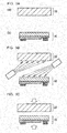
- a method of manufacturing a light emitting device includes a step of preparing a light emitting element 10 (see FIG. 3A(a) ), a step of preparing a wavelength converting member 20 (see FIG. 3A(b) ), and a bonding step for bonding the light emitting element 10 and the wavelength converting member 20 (see FIGS. 3B and 3C ) .
- the term "surface activated bonding technique” refers to that carrying out sputter etching by using ion beams or plasma on a bonding surface of a light emitting element 10 and a wavelength converting member 20 to activate both the surfaces to be bonded, then directly bond the light emitting element 10 and the wavelength converting member 20 at the bonding surfaces.
- the light emitting element 10 and the wavelength converting member 20 can be firmly bonded. This is considered as the result of sputter etching, the first region 11a and the third region 20a are formed and the both absorb the strain between the light emitting element 10 and the wavelength converting member 20 in an integrated manner (see FIG. 2 ). The details are as described above and will not be repeated here.
- a light emitting element is fabricated in such a manner that a column-shaped ingot of sapphire is thinly sliced to obtain disk-shaped wafers, and on each wafers, a plurality of semiconductor stacked layer portionas12 are formed and then divided into each of the light emitting elements.
- the wavelength converting member 20 is bonded to each of the light emitting element 10, by using a surface activated bonding technique.
- the use of the light emitting elements 10 which are already divided into single units has an advantage as described below (in the present specification, not only the state of individually divided unit but also the previous state of the wafer are also referred to a "light emitting element". That is, generally, the light emitting elements formed on a wafer have different properties such as the peak wavelength and/or optical output power depending on their locations on the wafer. However, such light emitting elements obtained by dividing the wafers can be grouped together by selecting the same or similar properties, and appropriate wavelength converting members 20 can be selected and bonded respectively thereto.
- Examples of specific steps include arranging a plurality of light emitting elements having similar properties on a single adhesive sheet (first step), bonding each of the light emitting elements arranged on the adhesive sheet with a single sheet of a wavelength converting member by using a surface activated bonding technique (second step), removing the adhesive sheet (third step), and cutting the wavelength converting member as needed to obtain individual light emitting devices (fourth step).
- Heating the light emitting element may result in deterioration of the electrodes and/or the light emitting layer, but a surface activated bonding technique is not necessarily heated.
- the light emitting element 10 and the wavelength converting member 20 can be bonded without deteriorating the properties of the light emitting element.
- the range of temperature to perform a surface activated bonding technique may be preferably 0° C. to 300° C., more preferably 0° C. to 200° C., further preferably 0° C. to 100° C., yet further preferably 0° C. to 50° C. With this arrangement, a firm bonding can be achieved without undermining the properties of the light emitting element.
- the bonding surfaces of the light emitting element 10 and the wavelength converting member 20 may have a surface roughness (Ra) of 10 nm or less, more preferably 5 nm or less, and further preferably 1 nm or less. Accordingly, the light emitting element 10 and the wavelength converting member 20 can be easily and firmly bonded.
- the wavelength converting member 20 is made of a fluorescent material, a support member (glass) and a bonding member (aluminum oxide), and the bonding member has, from the light emitting element side, a third region and a fourth region, and the third region has an irregular atomic arrangement compared with the fourth region.
- Respective layers of nitride semiconductor were grown on a sapphire substrate 11 to form a semiconductor stacked layer portion 12.
- An n-electrode 13 and a p-electrode 14 were formed on a part of a predetermined portion of the semiconductor stacked layer portion 12.
- the sapphire substrate in a wafer state was ground to reduce the thickness to about 85 micrometers.
- CMP Chemical Mechanical Polishing
- scratch marks left by the polishing are removed and the surface was smoothed to an Ra of 1 nm or less.
- the light emitting element in a wafer state obtained as described above was cut out by scrubbing to obtain individual light emitting elements 10.
- each light emitting element 10 of 1 mm long and 1 mm wide in a plan view was formed.
- Characterization such as voltage characteristic, wavelength, and leakage were carried out on each of the light emitting elements 10 and the light emitting elements 10 were sorted into groups on the basis of their characteristics.
- the light emitting elements 10 of respective groups were arranged on a respective adhesive sheet at an interval of 200 micrometers with each other.
- a wavelength converting member 20 formed by using an irreversible coagulation technique is prepared.
- the wavelength converting member 20 of the present example was made of a sapphire (support member) containing YAG (fluorescent material).
- the wavelength converting member 20 was ground and polished to a desired thickness.
- polishing and CMP were carried out.
- the sapphire portion becomes in a protruded shape and the YAG portion becomes a recesses shape, but in the present example, the difference in the height of the sapphire portion and the YAG portion is adjusted to 10 nm or less.
- the surface roughness of the YAG and the sapphire at the bonding surface were respectively adjusted to the Ra of 2 nm or less.
- the bonding chamber On the upper part of the bonding chamber, a plurality of the light emitting elements 10 were arranged on an adhesive sheet so that the sapphire substrates 11 which serve as the bonding surfaces locate to the underside. At the lower part of the bonding chamber, the wavelength converting member 20 was placed so that its bonding surface locates to the upper side.
- the bonding chamber was vacuumed to 8.0 ⁇ 10 -6 Pa or less. Then, using two fast ion beam (FAB: fast atom beam) guns, Ar ion beam was irradiated respectively on the upper and lower samples. Ar beam was irradiated with a flow rate of 40 scm, an acceleration current of 100 mA, and for 180 seconds. Then, the upper and lower samples were bonded within a short time of 30 seconds or less. At this time, a pressure of 0.2 N/mm 2 or more was applied on the samples for 30 seconds. The bonded sample was taken out from the bonding chamber and the adhesive sheet was removed from the sample.
- FAB fast atom beam
- a plurality of the light emitting elements 10 arranged on a single sheet of the wavelength converting member 20 are divided by dicing to obtain individual units of the light emitting devices.
- One of the light emitting device was mounted in a flip chip manner on a circuit board having electrodes and covered with a white resin made of titania particles dispersed in a silicone resin, except for the upper surface of the wavelength converting member 20 which serve as the light emitting surface.
- the light emitting devices obtained in the present example were confirmed to have approximately twice as much improvement in the die shear strength (bonding strength) as compared to the devices of Comparative Example. Further, compared to comparative Example, an approximately 10% improvement in the luminous flux was confirmed.
- the light emitting devices having substantially the same structure as in Example 1 were fabricated except that the sapphire substrate and the wavelength converting member were bonded by using an adhesive material made of a silicone resin.
- the light emitting device can be used, for example, for lighting devices and display devices.
- the invention may be embodied by the following exemplars:
Landscapes
- Led Device Packages (AREA)
- Led Devices (AREA)
Abstract
Description
- The present invention relates to a light emitting device in which a light emitting element and a wavelength converting member are bonded, and a method of manufacturing the light emitting device.
- Conventionally, there has been proposed is a light emitting device capable of emitting light of mixed color, by combining light from an LED chip which serves as a light emitting element and light from a fluorescent material which served as a wavelength converting member. For example, Patent Literature 1 describes that a "nucleation layer" made of GaN is grown on a growth substrate made of sapphire, and the "nucleation layer" and a "ceramic phosphor" are bonded at high temperature and high pressure.
- Patent Literature 1:
JP2006-352085A - However, there has been a problem that, in the light emitting device disclosed in Patent Literature 1, the "growth substrate" made of sapphire and the "nucleation layer" made of GaN are merely thermally compressed and the bonding strength was weak. It is undesirable because weak bonding strength may results in detachment of the growth substrate and the nucleation layer during use.
- Accordingly an object of the present invention is to provide a light emitting device having strong bonding strength between the light emitting element and the wavelength converting member. Means to Solve the Problems
- A light emitting device of an embodiment of the present invention includes a light emitting element and a wavelength converting member bonded with each other. Particularly, the light emitting element has, from the wavelength converting member side, a first region and a second region, the wavelength converting member has, from the light emitting element side, a third region and a fourth region, the first region has an irregular atomic arrangement compared with the second region, the third region has an irregular atomic arrangement compared with the fourth region, and the first region and the third region are directly bonded.
- According to an embodiment of the present invention, the light emitting element includes a substrate having the first region and the second region and a semiconductor stacked layer portion formed on the substrate. The wavelength converting member has a support member which has the third region and the fourth region and a fluorescent material which is contained in the support member.
- Further, according to an embodiment of the present invention, the substrate is made of sapphire and the support member is made of aluminum oxide.
- A method of manufacturing a light emitting device according to an embodiment of the present invention includes a step of preparing a light emitting element, a step of preparing a wavelength converting member, and a step of bonding the light emitting element and the wavelength converting member by using a surface activated bonding technique.
- It is preferable that the light emitting element has a substrate made of sapphire and a semiconductor stacked portion formed on the substrate, the wavelength converting member has a support member made of aluminum oxide and a fluorescent material contained in the support member, and the substrate and the support member are bonded in the bonding step.
- According to the present invention as described above, a light emitting device having strong bonding strength between the light emitting element and the wavelength converting member can be provided.
-
-
FIG. 1 is a diagram illustrating a cross section of a light emitting device according to the present invention. -
FIG. 2 is an enlarged view of the region ofFIG. 1 inside the broken lines. -
FIG. 3A(a) is a cross-sectional view illustrating a light emitting element preparation step of preparing alight emitting element 10 in a method of manufacturing a light emitting device according to an embodiment of the present invention, andFIG. 3A(b) is a cross-sectional view illustrating a wavelength converting member preparation step of preparing awavelength converting member 20. -
FIG. 3B is a cross sectional view illustrating a step of activating the bonding surface in a method of manufacturing a light emitting device according to an embodiment of the present invention. -
FIG. 3C is a cross-sectional view illustrating a bonding step of a method of manufacturing a light emitting device according to an embodiment of the present invention. - The embodiments of the present invention will be described below with reference to the accompanying drawings. The embodiments are intended as illustrative of a light emitting device to give a concrete form to technical ideas of the present invention, and the scope of the invention is not limited to those described below. Particularly, the sizes, materials, shapes and the relative positions of the members described in examples are given as an example and not as a limitation to the scope of the invention unless specifically stated. The sizes and the positional relationships of the members in each of the drawings are occasionally shown exaggerated for ease of explanation. Members same as or similar to those of this invention are assigned the same reference numerals and detailed description thereof will be omitted.
- In a light emitting device according to the present embodiment, a
light emitting element 10 and awavelength converting member 20 are bonded.FIG. 1 is a cross-sectional view in a direction perpendicular to a light emission observation surface of a light emitting device according to an embodiment.FIG. 2 is an enlarged view of the region ofFIG. 1 inside the broken line. In a light emitting device according to the present embodiment, alight emitting element 10 has, as shown inFIG. 1 for example, asubstrate 11 made of sapphire and a semiconductor stackedlayer portion 12 formed on thesubstrate 11, and a p-electrode 13 and an n-electrode 14 formed on the semiconductor stackedlayer portion 12. Thewavelength converting member 20 is made of a base member (support member) which serves as a base and a fluorescent material contained in the base member. In the present embodiment, thesubstrate 11 of thelight emitting element 10 has, from thewavelength converting member 20 side, afirst region 11a and asecond region 11b, and thewavelength converting member 20 has, from thelight emitting element 10 side, athird region 20a and afourth region 20b. In thesubstrate 11, thefirst region 11a has an irregular atomic arrangement compared with thesecond region 11b, and in thewavelength converting member 20, thethird region 20a has an irregular atomic arrangement compared with thefourth region 20b. Thefirst region 11a and thethird region 20a are directly bonded and thus thelight emitting element 10 and thewavelength converting member 20 are bonded. - As described above, in the present specification, the term "
first region 11a" indicates a region directly in contact with thewavelength converting member 20 in thelight emitting element 10. Also, the term "second region 11b" indicates a region abutting (directly in contact with) the "first region 11a" in thelight emitting element 10. In a same manner, the term "third region 20a" indicates a region of thewavelength converting member 20 which is directly in contact with thelight emitting element 10. Also, the term "fourth region 20b" indicates a region of thewavelength converting member 20 which is abutting the "third region 20a". As described above, thefirst region 11a having an irregular atomic arrangement compared with thesecond region 11b, and thethird region 20a having an irregular atomic arrangement compared with thefourth region 20b are directly in contact with each other and bonded to form a bonded interface X, and thesecond region 11b and thefourth region 20b are respectively spaced apart from the bonding interface X. In the present invention, thefirst region 11a and thesecond region 11b (thethird region 20a and thefourth region 20b) are abutted to each other, but the first region and the second region have the same composition. Thus, in the case where the members having different compositions are adjacent to each other, they are not indicated as the first region and the second region as in the present invention. More specifically, in the light emitting element having a sapphire substrate and an abutting semiconductor layer, there is no case where the semiconductor layer is indicated as the first region and the sapphire substrate is indicated as the second region. That is, thefirst region 11a and thesecond region 11b (thethird region 20a and thefourth region 20b) in the present specification are fundamentally a single member with the same composition, but a part of the member is indicated as the first region and a different part of the same member is indicated as the second region. Whether a part belongs to a certain member can be determined, for example, through a cross-sectional observation at atomic level by high-resolution transmission electron microscopy or through a comparison of composition from elemental analysis. - Accordingly, the
light emitting element 10 and thewavelength converting member 20 can be firmly bonded. Although the reason is not clear, it is considered that thefirst region 11a and thethird region 20a as a whole is capable of absorbing a strain developed between thelight emitting element 10 and thewavelength converting member 20. For example, in the case where thelight emitting element 10 and thewavelength converting member 20 are directly bonded through thermal compression, a strain may occur between the light emitting element10 and thewavelength converting member 20 due to differences in the lattice constant or in the thermal expansion coefficient. As described above, enhancing of the bonding strength between thelight emitting element 10 and thewavelength converting member 20 by way of thermal bonding has a limitation. However, it is thought that making the atomic arrangement of thefirst region 11a and thethird region 20a which are adjacent to the bonding interface X irregular than that of thesecond region 11b and thefourth region 20b enables to efficiently absorb the strain due to the difference in the lattice constant, the thermal expansion coefficient, or the like, and thus, the bonding strength is improved. It is also thought that a high unevenness in the atomic arrangement (preferably in an amorphous state which is in a non-equilibrium metastable state), anisotropic nature due to the crystal structure lessens and "weak "structures such as brittleness, crystal structure, and/or lattice defect which is attributed to the anisotropic nature disappears, and thus the bonding strength can be enhanced. Also, for example, in the case where thelight emitting element 10 and thewavelength converting member 20 are bonded through an adhesive agent made of a resin, strain may occur at each interface, because a resin has a relatively large thermal expansion. In contrast, the light emitting device according to the present embodiment does not require a resin to be interposed, so that a stronger bonding can be achieved. - Further, strain at the bonding interface X can be reduced through the
first region 11a and thethird region 20a, so that generation of stress in the fluorescent materials around the bonding interface X can be suppressed. Thewavelength converting member 20 contains a fluorescent material, so that stress associated with heat generation in the fluorescent material tends to occur. Generation of stress in the fluorescent material may cause an increase in the half bandwidth of the emission spectrum and decrease in the luminous flux, and thus undesirable. However, according to the present embodiment, an adverse influence of the strain on the fluorescent material can be reduced. In the present invention, thelight emitting element 10 and thewavelength converting member 20 are directly bonded. Therefore, compared with the case where thelight emitting element 10 and thewavelength converting member 20 are connected by an adhesive agent made of a resin which inherently has a poor thermal conductivity, it is also possible that the heat generated in thewavelength converting member 20 can be efficiently released to thelight emitting element 10 side. With this arrangement, a strain generated in the bonding surface X can be further reduced. - Further, directly bonding the
light emitting element 10 and thewavelength converting member 20 enables to reduce the number of the interfaces which reflect light (or totally reflect light depends on the angle of incidence) to one, and thus enables to improve the extraction of light as a whole device. For example, in the case where an adhesive made of a resin in interposed between the light emittingelement 10 and thewavelength converting member 20, a sum of two interfaces (an interface between the light emitting element and the adhesive agent and an interface between the wavelength converting member and the adhesive agent) exist. On the other hand, in the case where thelight emitting element 10 and thewavelength converting member 20 are directly bonded, only one interface (interface between the light emittingelement 10 and the wavelength converting member 20) exists. Therefore, compared to the former, the latter is capable of decrease the optical loss. Also, a use of an adhesive agent made of a resin results in a high reflectance at the interface due to a large difference in the refractive indices between the inorganic materials constituting the substrate and the resin which is an organic material. In contrast, the present invention is capable of reducing the difference in the refractive indices between thesubstrate 11 which constitutes a part of the light emitting element and thewavelength converting member 20, and thus reflection at the interface can be reduced. - The
first region 11a or thethird region 20a, or the both regions are preferably made of amorphous having higher atomic irregularity, and more preferably in a metastable, non-equilibrium amorphous state. With this arrangement, the strain between the light emittingelement 10 and thewavelength converting member 20 can be more efficiently prevented, anisotropy due to crystal structure can be further reduced, crystal structures and/or lattice defects can be eliminated, and the bonding strength can be further enhanced. - Either the
second region 11b or thefourth region 20b (preferably the both) may be preferably made of a polycrystal or a single crystal, more preferably made of a single crystal. Thesecond region 11b and/or thefourth region 20b being a polycrystal or a single crystal (particularly a single crystal) is thought to induce the strain therebetween. Thus, the present embodiment is particularly effective in such a state. - From a view point of reducing the strain, the
first region 11a and thethird region 20a are preferably disposed on substantially the entire area of the bonding interface X. However, in the present invention, the region to which thefirst region 11a and thethird region 20a are directly bonded may be a part of the bonding interface X, and which is in the scope of the present invention as long as it exerts the effects as described above. - The
first region 11a and thethird region 20a respectively have a thickness of preferably 1 nm to 20 nm, further preferably 2 nm to 10 nm. With this arrangement, the effect of reducing the strains can be sufficiently obtained, so that the bonding strength can be enhanced. Further, making thefirst region 11a and thethird region 20a with an irregular atomic arrangement may adversely affect the extraction of light, but in the range as described above, the thickness of the portion of optical attenuation can be substantially reduced, and thus optical loss can be reduced. - For the light emitting device according to the present embodiment, the
light emitting element 10 is not limited and a known light emitting element can be used. For example, as shown inFIG. 1 , thelight emitting element 10 may be include asubstrate 11, a semiconductor stackedlayer portion 12 disposed on thesubstrate 11, and a pair ofelectrodes layer portion 12. For thesubstrate 11, sapphire, GaN, or the like, can be employed. For the semiconductor stackedlayer portion 12, a stacked layer of a plurality of nitride semiconductor layers (AlInGaN), or the like, can be employed. In view of extraction of light, thewavelength converting member 20 side is preferably used as the viewing side. - In the case where sapphire is used as the
substrate 11 of thelight emitting element 10, it is preferable that the support member, which to be described later, of thewavelength converting member 20 is made of aluminum oxide and that the sapphire and the aluminum oxide are directly bonded. That is, thefirst region 11a and thesecond region 11b are formed in the sapphire and thethird region 20a and thefourth region 20b are formed in the aluminum oxide, and thefirst region 11a and thethird region 20a are directly bonded. - With this arrangement, the same compositional elements can be used for the substrate and the support member, so that bonding strength of the both can be further enhanced. Further, the refractive indices of the substrate and the support member can made substantially the same, so that the total reflection of light at the interface can be reduced and light extraction of the light emitting device can be improved. Although the effects described above can be achieved regardless of the crystal structures of aluminum oxide which constitutes the support member, the crystal structure of aluminum oxide may be preferably a polycrystal or a single crystal, more preferably a single crystal (sapphire). With this arrangement, a similar or the same structure as the substrate made of sapphire can be obtained and therefore the effects as described above can be easily obtained.
- In an other variant example, in a
light emitting element 10, after forming a semiconductor stacked layer portion on a substrate, a bonding substrate such as Si is adhered to the semiconductor stacked layer structure, then the initial substrate is removed and the bonding substrate and a wavelength converting member may be bonded. Further, regardless of whether a substrate is used, the semiconductor stacked layer portion and the wavelength converting member can be bonded. In the case where the semiconductor stacked layer portion and the wavelength converting member are bonded, one semiconductor layer at the most outer side of the semiconductor stacked layer portion to be bonded to the wavelength converting member has, from the wavelength converting member side, a first region and a second region, and the first region has an irregular atomic arrangement compared with the second region. - For the light emitting device according to the present embodiment, the
wavelength converting member 20 is capable of converting light from thelight emitting element 10 into light having different wavelength distribution, and the material thereof is not limited, and a known material can be used. Thewavelength converting member 20 may be a fluorescent material, or may includes a fluorescent material and a support member which support the fluorescent material. In the case where thewavelength converting member 20 includes a fluorescent material and a support member, for example, thewavelength converting member 20 is an eutectic of a fluorescent material and a support member formed by using an irreversible coagulation technique, or thewavelength converting member 20 is integrally formed by sintering a fluorescent material powder and a material powder of the support member. - The fluorescent material is not limited and a known fluorescent material can be used. For example, a YAG (yttrium aluminum garnet) based fluorescent material and/or a TAG (terbium aluminum garnet) based fluorescent material may be used. With this arrangement, for example, by mixing blue emission from the
light emitting element 10 and yellow emission from the fluorescent material, white light can be emitted. - The support member is not limited and a known support member can be used. For example, aluminum oxide, aluminum nitride, YAG (non-luminous, because an activator is not contained), and/or yttrium oxide can be used.
- The fluorescent material has a base member and an activator, and the support member is preferably made of the same materials as the base member. With this arrangement, the difference in the refractive indices between the fluorescent material and the support member can be substantially eliminated. As a result, total reflection of light at the interface between the support member and the fluorescent material can be substantially reduced, and the light extraction efficiency as the entire light emitting device can be improved. Further, employing the same materials for the support member and the base member enables to reduce the stress generated in the fluorescent material. For example, a YAG (non-luminous, because an activator is not contained) can be used for the support member and a so-called YAG-based fluorescent material with cerium as the activator and a YAG as the base member, can be used for the fluorescent material.
- As shown in
FIG. 3 , a method of manufacturing a light emitting device according to an embodiment of the present invention includes a step of preparing a light emitting element 10 (seeFIG. 3A(a) ), a step of preparing a wavelength converting member 20 (seeFIG. 3A(b) ), and a bonding step for bonding thelight emitting element 10 and the wavelength converting member 20 (seeFIGS. 3B and 3C ) . - In the present embodiment, the term "surface activated bonding technique" refers to that carrying out sputter etching by using ion beams or plasma on a bonding surface of a
light emitting element 10 and awavelength converting member 20 to activate both the surfaces to be bonded, then directly bond thelight emitting element 10 and thewavelength converting member 20 at the bonding surfaces. - Accordingly, the
light emitting element 10 and thewavelength converting member 20 can be firmly bonded. This is considered as the result of sputter etching, thefirst region 11a and thethird region 20a are formed and the both absorb the strain between the light emittingelement 10 and thewavelength converting member 20 in an integrated manner (seeFIG. 2 ). The details are as described above and will not be repeated here. - Generally, a light emitting element is fabricated in such a manner that a column-shaped ingot of sapphire is thinly sliced to obtain disk-shaped wafers, and on each wafers, a plurality of semiconductor stacked layer portionas12 are formed and then divided into each of the light emitting elements. In the present invention, at the time of bonding the
light emitting element 10 and thewavelength converting member 20 by using a surface activated bonding technique, prior to dividing into each of the light emitting elements, a wafer on which a plurality of semiconductor stackedlayer portions 12 are formed and thewavelength converting member 20 may be bonded, or after dividing into each of the light emitting elements, thewavelength converting member 20 is bonded to each of thelight emitting element 10, by using a surface activated bonding technique. However, in the case where thelight emitting element 10 and thewavelength converting member 20 are bonded by using a surface activated bonding technique, the use of thelight emitting elements 10 which are already divided into single units has an advantage as described below (in the present specification, not only the state of individually divided unit but also the previous state of the wafer are also referred to a "light emitting element". That is, generally, the light emitting elements formed on a wafer have different properties such as the peak wavelength and/or optical output power depending on their locations on the wafer. However, such light emitting elements obtained by dividing the wafers can be grouped together by selecting the same or similar properties, and appropriatewavelength converting members 20 can be selected and bonded respectively thereto. Examples of specific steps include arranging a plurality of light emitting elements having similar properties on a single adhesive sheet (first step), bonding each of the light emitting elements arranged on the adhesive sheet with a single sheet of a wavelength converting member by using a surface activated bonding technique (second step), removing the adhesive sheet (third step), and cutting the wavelength converting member as needed to obtain individual light emitting devices (fourth step). - Heating the light emitting element may result in deterioration of the electrodes and/or the light emitting layer, but a surface activated bonding technique is not necessarily heated. Thus, the
light emitting element 10 and thewavelength converting member 20 can be bonded without deteriorating the properties of the light emitting element. Although according to the materials and construction of the electrodes and the material and the construction of the semiconductor stacked layer portion, the range of temperature to perform a surface activated bonding technique may be preferably 0° C. to 300° C., more preferably 0° C. to 200° C., further preferably 0° C. to 100° C., yet further preferably 0° C. to 50° C. With this arrangement, a firm bonding can be achieved without undermining the properties of the light emitting element. - The bonding surfaces of the
light emitting element 10 and thewavelength converting member 20 may have a surface roughness (Ra) of 10 nm or less, more preferably 5 nm or less, and further preferably 1 nm or less. Accordingly, thelight emitting element 10 and thewavelength converting member 20 can be easily and firmly bonded. - Though, depending on the material and state of the bonding surface of the
light emitting element 10 and the bonding surface of thewavelength converting member 20, bonding of the both by using a surface activated bonding technique may be difficult. Even in such a case, forming a bonding member capable of bonding to the both on one or both of thelight emitting element 10 and thewavelength converting member 20 enables bonding of the both. For example, with a use of surface activated bonding technique, a glass (including a fluorescent material) is difficult to be bonded to the sapphire substrate of the light emitting element. For this reason, a bonding member such as aluminum oxide is formed on the glass surface by using sputtering or the like, which enables bonding of aluminum oxide and the sapphire substrate by using a surface activated bonding technique. In this case, thewavelength converting member 20 is made of a fluorescent material, a support member (glass) and a bonding member (aluminum oxide), and the bonding member has, from the light emitting element side, a third region and a fourth region, and the third region has an irregular atomic arrangement compared with the fourth region. - Respective layers of nitride semiconductor were grown on a
sapphire substrate 11 to form a semiconductor stackedlayer portion 12. An n-electrode 13 and a p-electrode 14 were formed on a part of a predetermined portion of the semiconductor stackedlayer portion 12. The sapphire substrate in a wafer state was ground to reduce the thickness to about 85 micrometers. Further, using a CMP (Chemical Mechanical Polishing) technique, scratch marks left by the polishing are removed and the surface was smoothed to an Ra of 1 nm or less. The light emitting element in a wafer state obtained as described above was cut out by scrubbing to obtain individuallight emitting elements 10. In the present example, eachlight emitting element 10 of 1 mm long and 1 mm wide in a plan view was formed. - Characterization such as voltage characteristic, wavelength, and leakage were carried out on each of the
light emitting elements 10 and thelight emitting elements 10 were sorted into groups on the basis of their characteristics. Thelight emitting elements 10 of respective groups were arranged on a respective adhesive sheet at an interval of 200 micrometers with each other. - A
wavelength converting member 20 formed by using an irreversible coagulation technique is prepared. Thewavelength converting member 20 of the present example was made of a sapphire (support member) containing YAG (fluorescent material). In conformity with the chromaticity of a desired white LED (light emitting device), thewavelength converting member 20 was ground and polished to a desired thickness. Next, in order to further smooth the surface which is to serve as the bonding surface, polishing and CMP were carried out. At this time, due to the difference in the polishing rate, the sapphire portion becomes in a protruded shape and the YAG portion becomes a recesses shape, but in the present example, the difference in the height of the sapphire portion and the YAG portion is adjusted to 10 nm or less. The surface roughness of the YAG and the sapphire at the bonding surface were respectively adjusted to the Ra of 2 nm or less. - On the upper part of the bonding chamber, a plurality of the
light emitting elements 10 were arranged on an adhesive sheet so that thesapphire substrates 11 which serve as the bonding surfaces locate to the underside. At the lower part of the bonding chamber, thewavelength converting member 20 was placed so that its bonding surface locates to the upper side. - The bonding chamber was vacuumed to 8.0 × 10⁻⁶ Pa or less. Then, using two fast ion beam (FAB: fast atom beam) guns, Ar ion beam was irradiated respectively on the upper and lower samples. Ar beam was irradiated with a flow rate of 40 scm, an acceleration current of 100 mA, and for 180 seconds. Then, the upper and lower samples were bonded within a short time of 30 seconds or less. At this time, a pressure of 0.2 N/mm2 or more was applied on the samples for 30 seconds. The bonded sample was taken out from the bonding chamber and the adhesive sheet was removed from the sample.
- A plurality of the
light emitting elements 10 arranged on a single sheet of thewavelength converting member 20 are divided by dicing to obtain individual units of the light emitting devices. One of the light emitting device was mounted in a flip chip manner on a circuit board having electrodes and covered with a white resin made of titania particles dispersed in a silicone resin, except for the upper surface of thewavelength converting member 20 which serve as the light emitting surface. - The light emitting devices obtained in the present example were confirmed to have approximately twice as much improvement in the die shear strength (bonding strength) as compared to the devices of Comparative Example. Further, compared to comparative Example, an approximately 10% improvement in the luminous flux was confirmed.
- The light emitting devices having substantially the same structure as in Example 1 were fabricated except that the sapphire substrate and the wavelength converting member were bonded by using an adhesive material made of a silicone resin.
- The light emitting device according to an embodiment of the present invention can be used, for example, for lighting devices and display devices. In summary the invention may be embodied by the following exemplars:
- 1. A light emitting device comprising: a light emitting element and a wavelength converting member bonded with each other; wherein
the light emitting element has, from the wavelength converting member side, a first region and a second region;
the wavelength converting member has, from the light emitting element side, a third region and a fourth region;
the first region has an irregular atomic arrangement compared with the second region; the third region has an irregular atomic arrangement compared with the fourth region, and the first region and the third region are directly bonded. - 2. The light emitting device according to exemplar 1, wherein the light emitting element comprises a substrate having the first region and the second region and a semiconductor stacked layer portion formed on the substrate, and the wavelength converting member has a support member which has the third region and the fourth region and a fluorescent material which is contained in the support member.
- 3. The light emitting device according to exemplar 2, wherein the substrate is made of sapphire and the support member is made of aluminum oxide.
- 4. A method of manufacturing a light emitting device comprising steps of:
- preparing a light emitting element;
- preparing a wavelength converting member; and
- bonding the light emitting element and the wavelength converting member by using a surface activated bonding technique.
- 5. The method of manufacturing a light emitting device according to exemplar 4, wherein the light emitting element has a substrate made of sapphire, and a semiconductor stacked layer portion formed on the substrate, and the wavelength converting member has a support member made of aluminum oxide, and a fluorescent material contained in the support member, and wherein in the step of bonding, the substrate and the support member are bonded.
-
- 10 ···
- light emitting element
- 11 ···
- substrate
- 11a ···
- first region
- 11b ···
- second region
- 12 ···
- semiconductor stacked layer portion
- 13 ···
- p-electrode
- 14 ···
- n-electrode
- 20 ···
- wavelength converting member
- 20a ···
- third region
- 20b ···
- fourth region
Claims (7)
- A method of manufacturing a light emitting device comprising steps of:preparing a light emitting element;preparing a wavelength converting member;sputter etching by using ion beams on a bonding surface of the light emitting element and a bonding surface of the wavelength converting member to activate both the bonding surfaces; and thendirectly bonding the light emitting element and the wavelength converting member at the bonding surfaces.
- The method of manufacturing a light emitting device according to claim 1,
wherein the light emitting element comprises a substrate made of sapphire, and a semiconductor stacked layer portion formed on the substrate, and the wavelength converting member comprises a support member made of aluminum oxide, and a fluorescent material supported by the support member, and
wherein the substrate and the support member are directly bonded. - The method of manufacturing a light emitting device according to claim 2,
wherein the fluorescent material comprises one of an yttrium aluminum garnet based fluorescent material and a terbium aluminum garnet based fluorescent material. - The method of manufacturing a light emitting device according to any one of claims 1-3,
wherein a temperature to perform sputter etching and directly bonding is set
not less than 0° C nor more than 300° C, or
not less than 0° C nor more than 200° C, or
not less than 0° C nor more than 100° C, or
not less than 0° C nor more than 50 ° C. - The method of manufacturing a light emitting device according to any one of claims 1-4,
wherein the bonding surfaces of the light emitting element and the wavelength converting member have a surface roughness (Ra) of10 nm or less, or5 nm or less, or1 nm or less. - The method of manufacturing a light emitting device according to claim 2 or 3, or according to claim 4 or 5 referring to claim 2 or 3,
wherein a bonding surface of the wavelength converting member includes aluminum oxide portions and fluorescent material portions, and the difference in the height of the aluminum oxide portion and the YAG portion is 10 nm or less. - The method of manufacturing a light emitting device according to claim 1,
wherein the light emitting element comprises a substrate comprising a first region and a second region from the wavelength converting member side, and the wavelength converting member comprises a third region and a fourth region from the light emitting element side, and
wherein the first region and the third region have a thickness not less than 1 nm nor more than 20 nm, or
not less than 2 nm nor more than 10 nm.
Applications Claiming Priority (3)
| Application Number | Priority Date | Filing Date | Title |
|---|---|---|---|
| JP2010089267 | 2010-04-08 | ||
| PCT/JP2011/058586 WO2011126000A1 (en) | 2010-04-08 | 2011-04-05 | Light-emitting device and process for production thereof |
| EP11765900.3A EP2557607B1 (en) | 2010-04-08 | 2011-04-05 | Light-emitting device and process for production thereof |
Related Parent Applications (2)
| Application Number | Title | Priority Date | Filing Date |
|---|---|---|---|
| EP11765900.3A Division-Into EP2557607B1 (en) | 2010-04-08 | 2011-04-05 | Light-emitting device and process for production thereof |
| EP11765900.3A Division EP2557607B1 (en) | 2010-04-08 | 2011-04-05 | Light-emitting device and process for production thereof |
Publications (1)
| Publication Number | Publication Date |
|---|---|
| EP3509113A1 true EP3509113A1 (en) | 2019-07-10 |
Family
ID=44762936
Family Applications (2)
| Application Number | Title | Priority Date | Filing Date |
|---|---|---|---|
| EP11765900.3A Active EP2557607B1 (en) | 2010-04-08 | 2011-04-05 | Light-emitting device and process for production thereof |
| EP19152171.5A Pending EP3509113A1 (en) | 2010-04-08 | 2011-04-05 | Method of manufacturing the light emitting device |
Family Applications Before (1)
| Application Number | Title | Priority Date | Filing Date |
|---|---|---|---|
| EP11765900.3A Active EP2557607B1 (en) | 2010-04-08 | 2011-04-05 | Light-emitting device and process for production thereof |
Country Status (9)
| Country | Link |
|---|---|
| US (3) | US8916399B2 (en) |
| EP (2) | EP2557607B1 (en) |
| JP (1) | JPWO2011126000A1 (en) |
| KR (3) | KR102109668B1 (en) |
| CN (1) | CN102823000B (en) |
| BR (1) | BR112012025660B1 (en) |
| RU (1) | RU2528604C2 (en) |
| TW (1) | TWI521746B (en) |
| WO (1) | WO2011126000A1 (en) |
Families Citing this family (32)
| Publication number | Priority date | Publication date | Assignee | Title |
|---|---|---|---|---|
| JPWO2011126000A1 (en) * | 2010-04-08 | 2013-07-11 | 日亜化学工業株式会社 | Light emitting device and manufacturing method thereof |
| JP2012142326A (en) * | 2010-12-28 | 2012-07-26 | Mitsubishi Heavy Ind Ltd | Light-emitting device and method of manufacturing light-emitting device |
| DE102011014845B4 (en) * | 2011-03-23 | 2023-05-17 | OSRAM Opto Semiconductors Gesellschaft mit beschränkter Haftung | Semiconductor light-emitting device and method of manufacturing a semiconductor light-emitting device |
| WO2014111822A1 (en) | 2013-01-16 | 2014-07-24 | Koninklijke Philips N.V. | Led using luminescent sapphire as down-converter |
| EP2979309A1 (en) * | 2013-03-29 | 2016-02-03 | Koninklijke Philips N.V. | Light emitting device comprising wavelength converter |
| JP2014225636A (en) * | 2013-04-16 | 2014-12-04 | 株式会社ディスコ | Light-emitting device |
| JP6414391B2 (en) * | 2013-04-30 | 2018-10-31 | 日亜化学工業株式会社 | Method for manufacturing light emitting device |
| KR102185099B1 (en) * | 2013-05-20 | 2020-12-02 | 루미리즈 홀딩 비.브이. | Chip scale light emitting device package with dome |
| JP6299478B2 (en) | 2013-06-26 | 2018-03-28 | 日亜化学工業株式会社 | Light emitting device and manufacturing method thereof |
| CN104332539B (en) * | 2013-07-22 | 2017-10-24 | 中国科学院福建物质结构研究所 | GaN base LED epitaxial structure and its manufacture method |
| JP6387780B2 (en) | 2013-10-28 | 2018-09-12 | 日亜化学工業株式会社 | Light emitting device and manufacturing method thereof |
| JP6438648B2 (en) * | 2013-11-15 | 2018-12-19 | 日亜化学工業株式会社 | Semiconductor light emitting device and manufacturing method thereof |
| JP6749240B2 (en) * | 2014-01-09 | 2020-09-02 | ルミレッズ ホールディング ベーフェー | Light emitting device with reflective sidewalls |
| JP6176171B2 (en) | 2014-03-28 | 2017-08-09 | 豊田合成株式会社 | Method for manufacturing light emitting device |
| JP6398323B2 (en) | 2014-05-25 | 2018-10-03 | 日亜化学工業株式会社 | Manufacturing method of semiconductor light emitting device |
| EP2953176A1 (en) * | 2014-06-02 | 2015-12-09 | Swarovski Energy GmbH | Lighting device |
| JP6515515B2 (en) * | 2014-12-11 | 2019-05-22 | 日亜化学工業株式会社 | Manufacturing method of light emitting device |
| WO2016185860A1 (en) * | 2015-05-15 | 2016-11-24 | ソニー株式会社 | Phosphor substrate, light source device, and projection display device |
| JP2017220652A (en) * | 2016-06-10 | 2017-12-14 | 大学共同利用機関法人自然科学研究機構 | Laser apparatus and manufacturing method thereof |
| WO2017217486A1 (en) * | 2016-06-16 | 2017-12-21 | 日本碍子株式会社 | Phosphor element and lighting device |
| JP6724639B2 (en) | 2016-08-01 | 2020-07-15 | 日亜化学工業株式会社 | Light emitting device |
| JP6245587B1 (en) * | 2016-10-28 | 2017-12-13 | 大学共同利用機関法人自然科学研究機構 | Laser parts |
| DE102017101091A1 (en) | 2017-01-20 | 2018-07-26 | Osram Gmbh | CONVERTER, LASER ACTIVATED REMOTE PHOSPHOR (LARP) SYSTEM, HEADLIGHTS AND PROCESS |
| JP6579141B2 (en) | 2017-03-24 | 2019-09-25 | 日亜化学工業株式会社 | Light emitting device and method for manufacturing light emitting device |
| JP7111939B2 (en) | 2017-04-28 | 2022-08-03 | 日亜化学工業株式会社 | Light emitting device and manufacturing method thereof |
| JP6854715B2 (en) | 2017-06-30 | 2021-04-07 | 日亜化学工業株式会社 | Manufacturing method of light emitting device |
| US10128419B1 (en) | 2017-08-03 | 2018-11-13 | Lumileds Llc | Method of manufacturing a light emitting device |
| EP3582271B1 (en) * | 2018-06-14 | 2021-03-17 | Nichia Corporation | Light emitting device and method of manufacturing same |
| JP7343749B2 (en) * | 2018-06-14 | 2023-09-13 | 日亜化学工業株式会社 | Light emitting device and its manufacturing method |
| US11933489B2 (en) | 2020-02-07 | 2024-03-19 | Stanley Electric Co., Ltd. | Optical device, and method of fabricating optical device |
| JP7469641B2 (en) * | 2020-05-20 | 2024-04-17 | 日亜化学工業株式会社 | Light-emitting device inspection method and inspection tool |
| CN113808925A (en) * | 2021-09-28 | 2021-12-17 | 包头稀土研发中心 | Composite structure fluorescent substrate, composite method and flip LED structure |
Citations (9)
| Publication number | Priority date | Publication date | Assignee | Title |
|---|---|---|---|---|
| JPH11248656A (en) * | 1998-03-02 | 1999-09-17 | Nec Corp | Method for analyzing composition distribution in direction of depth |
| EP1191608A2 (en) * | 2000-09-12 | 2002-03-27 | LumiLeds Lighting U.S., LLC | Light emitting diodes with improved light extraction efficiency |
| KR20060130394A (en) * | 2005-06-14 | 2006-12-19 | 삼성전기주식회사 | Phosphor film production method, light emitting device manufacturing method and light emitting device using same |
| JP2006352085A (en) | 2005-03-14 | 2006-12-28 | Philips Lumileds Lightng Co Llc | Wavelength conversion type semiconductor light emitting device |
| EP1986217A1 (en) * | 2006-02-16 | 2008-10-29 | Shin-Etsu Chemical Co., Ltd. | Method for manufacturing semiconductor substrate |
| EP1988575A2 (en) * | 2007-03-26 | 2008-11-05 | Semiconductor Energy Laboratory Co., Ltd. | Semiconductor device |
| JP2009289835A (en) * | 2008-05-27 | 2009-12-10 | Panasonic Electric Works Co Ltd | Method for manufacturing structure, and method for manufacturing light-emitting device |
| US20100019260A1 (en) * | 2008-07-24 | 2010-01-28 | Koninklijke Philips Electronics N.V. | Semiconductor light emitting device including a window layer and a light-directing structure |
| EP2154709A2 (en) * | 2008-08-11 | 2010-02-17 | Sumitomo Electric Industries, Ltd. | Method of manufacturing group III nitride semiconductor layer bonded substrate |
Family Cites Families (30)
| Publication number | Priority date | Publication date | Assignee | Title |
|---|---|---|---|---|
| JPH0810672B2 (en) * | 1987-07-03 | 1996-01-31 | 富士通株式会社 | Flat plate bonding method |
| JPH11307813A (en) | 1998-04-03 | 1999-11-05 | Hewlett Packard Co <Hp> | Light emitting device, manufacturing method thereof and display |
| JP2000340509A (en) | 1999-05-26 | 2000-12-08 | Sumitomo Electric Ind Ltd | GaN substrate and method of manufacturing the same |
| JP2002141559A (en) | 2000-10-31 | 2002-05-17 | Sanken Electric Co Ltd | Light emitting semiconductor chip assembly and light emitting semiconductor lead frame |
| US7554258B2 (en) | 2002-10-22 | 2009-06-30 | Osram Opto Semiconductors Gmbh | Light source having an LED and a luminescence conversion body and method for producing the luminescence conversion body |
| CN1738781A (en) | 2003-01-20 | 2006-02-22 | 宇部兴产株式会社 | Ceramic composites for light conversion and their applications |
| JP3913700B2 (en) | 2003-04-08 | 2007-05-09 | 富士通メディアデバイス株式会社 | Surface acoustic wave device and manufacturing method thereof |
| RU2261502C1 (en) * | 2004-02-05 | 2005-09-27 | Открытое акционерное общество "Научно-исследовательский институт ГИРИКОНД" | Photo-luminescent emitter, semiconductor element and optron based on said devices |
| US7361938B2 (en) * | 2004-06-03 | 2008-04-22 | Philips Lumileds Lighting Company Llc | Luminescent ceramic for a light emitting device |
| JP4420021B2 (en) * | 2004-06-24 | 2010-02-24 | 宇部興産株式会社 | White light emitting diode device |
| JP2006100787A (en) | 2004-08-31 | 2006-04-13 | Toyoda Gosei Co Ltd | Light emitting device and light emitting element |
| EP1797594A2 (en) * | 2004-09-28 | 2007-06-20 | Philips Intellectual Property & Standards GmbH | Light emitting device with improved conversion layer |
| CN100521171C (en) * | 2004-10-21 | 2009-07-29 | 财团法人工业技术研究院 | Packaging and connecting structure of element |
| JP5021213B2 (en) | 2006-01-23 | 2012-09-05 | 昭和電工株式会社 | Light emitting diode and manufacturing method thereof |
| US8592858B2 (en) | 2006-01-23 | 2013-11-26 | Showa Denko K.K. | Light-emitting diode and method for fabrication thereof |
| KR20090017696A (en) | 2006-06-08 | 2009-02-18 | 코닌클리즈케 필립스 일렉트로닉스 엔.브이. | Light emitting device and display device including same |
| CN100578826C (en) | 2006-08-09 | 2010-01-06 | 广东昭信光电科技有限公司 | A kind of preparation method of white light-emitting diode chip |
| US7521862B2 (en) * | 2006-11-20 | 2009-04-21 | Philips Lumileds Lighting Co., Llc | Light emitting device including luminescent ceramic and light-scattering material |
| US7687823B2 (en) * | 2006-12-26 | 2010-03-30 | Nichia Corporation | Light-emitting apparatus and method of producing the same |
| JP5070557B2 (en) | 2007-02-27 | 2012-11-14 | 武仁 島津 | Room temperature bonding method |
| JP2009105123A (en) | 2007-10-22 | 2009-05-14 | Showa Denko Kk | Light emitting diode and manufacturing method thereof |
| JP2009114953A (en) | 2007-11-06 | 2009-05-28 | Nissan Motor Co Ltd | MICRONOZZLE FOR FUEL INJECTION DEVICE AND METHOD FOR MANUFACTURING MICRO NOZZLE FOR FUEL INJECTION DEVICE |
| KR101517644B1 (en) | 2007-11-29 | 2015-05-04 | 니치아 카가쿠 고교 가부시키가이샤 | Light-emitting device and its manufacturing method |
| JP5315070B2 (en) | 2008-02-07 | 2013-10-16 | 昭和電工株式会社 | Compound semiconductor light emitting diode |
| JP5307881B2 (en) | 2008-03-26 | 2013-10-02 | パナソニック株式会社 | Semiconductor light emitting device |
| JP4911143B2 (en) | 2008-08-15 | 2012-04-04 | 信越化学工業株式会社 | High temperature resistant adhesive composition, substrate bonding method, and three-dimensional semiconductor device |
| JP2010287687A (en) * | 2009-06-10 | 2010-12-24 | Koito Mfg Co Ltd | Light emitting module and method for manufacturing light emitting module |
| JP2009260391A (en) * | 2009-08-05 | 2009-11-05 | Sumitomo Electric Ind Ltd | Group-iii nitride semiconductor layer-bonded substrate and method of manufacturing semiconductor device |
| JP2011109002A (en) * | 2009-11-20 | 2011-06-02 | Citizen Holdings Co Ltd | Integrated device and manufacturing method therefor |
| JPWO2011126000A1 (en) | 2010-04-08 | 2013-07-11 | 日亜化学工業株式会社 | Light emitting device and manufacturing method thereof |
-
2011
- 2011-04-05 JP JP2012509662A patent/JPWO2011126000A1/en active Pending
- 2011-04-05 EP EP11765900.3A patent/EP2557607B1/en active Active
- 2011-04-05 KR KR1020187021215A patent/KR102109668B1/en active Active
- 2011-04-05 RU RU2012147484/28A patent/RU2528604C2/en active
- 2011-04-05 KR KR1020127029192A patent/KR20130029387A/en not_active Ceased
- 2011-04-05 CN CN201180016791.1A patent/CN102823000B/en active Active
- 2011-04-05 EP EP19152171.5A patent/EP3509113A1/en active Pending
- 2011-04-05 BR BR112012025660-2A patent/BR112012025660B1/en active IP Right Grant
- 2011-04-05 US US13/639,759 patent/US8916399B2/en active Active
- 2011-04-05 WO PCT/JP2011/058586 patent/WO2011126000A1/en not_active Ceased
- 2011-04-05 KR KR1020207012969A patent/KR102285141B1/en active Active
- 2011-04-08 TW TW100112330A patent/TWI521746B/en active
-
2014
- 2014-11-25 US US14/553,578 patent/US9293642B2/en active Active
- 2014-11-25 US US14/553,628 patent/US9293643B2/en active Active
Patent Citations (9)
| Publication number | Priority date | Publication date | Assignee | Title |
|---|---|---|---|---|
| JPH11248656A (en) * | 1998-03-02 | 1999-09-17 | Nec Corp | Method for analyzing composition distribution in direction of depth |
| EP1191608A2 (en) * | 2000-09-12 | 2002-03-27 | LumiLeds Lighting U.S., LLC | Light emitting diodes with improved light extraction efficiency |
| JP2006352085A (en) | 2005-03-14 | 2006-12-28 | Philips Lumileds Lightng Co Llc | Wavelength conversion type semiconductor light emitting device |
| KR20060130394A (en) * | 2005-06-14 | 2006-12-19 | 삼성전기주식회사 | Phosphor film production method, light emitting device manufacturing method and light emitting device using same |
| EP1986217A1 (en) * | 2006-02-16 | 2008-10-29 | Shin-Etsu Chemical Co., Ltd. | Method for manufacturing semiconductor substrate |
| EP1988575A2 (en) * | 2007-03-26 | 2008-11-05 | Semiconductor Energy Laboratory Co., Ltd. | Semiconductor device |
| JP2009289835A (en) * | 2008-05-27 | 2009-12-10 | Panasonic Electric Works Co Ltd | Method for manufacturing structure, and method for manufacturing light-emitting device |
| US20100019260A1 (en) * | 2008-07-24 | 2010-01-28 | Koninklijke Philips Electronics N.V. | Semiconductor light emitting device including a window layer and a light-directing structure |
| EP2154709A2 (en) * | 2008-08-11 | 2010-02-17 | Sumitomo Electric Industries, Ltd. | Method of manufacturing group III nitride semiconductor layer bonded substrate |
Non-Patent Citations (1)
| Title |
|---|
| TAKAGI H ET AL: "Direct bonding of two crystal substrates at room temperature by Ar-beam surface activation", JOURNAL OF CRYSTAL GROWTH, ELSEVIER, AMSTERDAM, NL, vol. 292, no. 2, 1 July 2006 (2006-07-01), pages 429 - 432, XP028016470, ISSN: 0022-0248, [retrieved on 20060701], DOI: 10.1016/J.JCRYSGRO.2006.04.049 * |
Also Published As
| Publication number | Publication date |
|---|---|
| JPWO2011126000A1 (en) | 2013-07-11 |
| CN102823000A (en) | 2012-12-12 |
| US8916399B2 (en) | 2014-12-23 |
| US20130026527A1 (en) | 2013-01-31 |
| KR102109668B1 (en) | 2020-05-12 |
| CN102823000B (en) | 2016-08-03 |
| KR102285141B1 (en) | 2021-08-04 |
| US20150118771A1 (en) | 2015-04-30 |
| EP2557607B1 (en) | 2019-02-20 |
| KR20180086303A (en) | 2018-07-30 |
| TW201205897A (en) | 2012-02-01 |
| US20150076548A1 (en) | 2015-03-19 |
| BR112012025660A2 (en) | 2016-06-28 |
| KR20130029387A (en) | 2013-03-22 |
| BR112012025660B1 (en) | 2021-12-21 |
| EP2557607A4 (en) | 2015-11-04 |
| TWI521746B (en) | 2016-02-11 |
| KR20200052981A (en) | 2020-05-15 |
| US9293642B2 (en) | 2016-03-22 |
| RU2528604C2 (en) | 2014-09-20 |
| EP2557607A1 (en) | 2013-02-13 |
| RU2012147484A (en) | 2014-05-20 |
| US9293643B2 (en) | 2016-03-22 |
| WO2011126000A1 (en) | 2011-10-13 |
Similar Documents
| Publication | Publication Date | Title |
|---|---|---|
| EP2557607B1 (en) | Light-emitting device and process for production thereof | |
| CN105390580B (en) | Light emitting semiconductor device | |
| JP5461887B2 (en) | LIGHT EMITTING ELEMENT AND LIGHT EMITTING DEVICE MANUFACTURING METHOD | |
| EP2819188B1 (en) | Light-emitting device and manufacturing method thereof | |
| US20100047944A1 (en) | Light-emitting element with improved light extraction efficiency, light-emitting device including the same, and methods of fabricating light-emitting element and light-emitting device | |
| US9935244B2 (en) | Light emitting device including a filter and a protective layer | |
| US20080042150A1 (en) | White Light Emitting Device and Method for Manufacturing the Same | |
| JP2013251417A (en) | Light-emitting device | |
| JP2012060180A (en) | Light-emitting ceramic for light-emitting device | |
| US12140304B2 (en) | Phosphor element with heat dissipating substrate that has thermally conductive metal plating film | |
| US8921130B2 (en) | Methods for producing and placing wavelength converting structures | |
| KR20100008656A (en) | Fabricating methods of the light emitting element and the light emitting device, the light emitting element and the light emitting device fabricated by the methods | |
| JP2007266571A (en) | LED chip, manufacturing method thereof, and light emitting device | |
| WO2010082396A1 (en) | Substrate for light-emitting element | |
| JP2005072527A (en) | Light emitting element and its manufacturing method | |
| TWI476956B (en) | Semiconductor light emitting element and manufacturing method thereof | |
| WO2011162236A1 (en) | Substrate, method for producing substrate, and light emitting element | |
| JP7483197B2 (en) | Light emitting device and method for manufacturing the same | |
| TW200539481A (en) | Group Ⅲ nitride semiconductor light-emitting device, forming method thereof, lamp and light source using same | |
| JP7343749B2 (en) | Light emitting device and its manufacturing method | |
| JP2023172001A (en) | Wavelength conversion member, light emitting device, and method for manufacturing wavelength conversion member | |
| KR20210116402A (en) | Method of manufacturing glass member for light wavelenghth conversion |
Legal Events
| Date | Code | Title | Description |
|---|---|---|---|
| PUAI | Public reference made under article 153(3) epc to a published international application that has entered the european phase |
Free format text: ORIGINAL CODE: 0009012 |
|
| STAA | Information on the status of an ep patent application or granted ep patent |
Free format text: STATUS: THE APPLICATION HAS BEEN PUBLISHED |
|
| AC | Divisional application: reference to earlier application |
Ref document number: 2557607 Country of ref document: EP Kind code of ref document: P |
|
| AK | Designated contracting states |
Kind code of ref document: A1 Designated state(s): AL AT BE BG CH CY CZ DE DK EE ES FI FR GB GR HR HU IE IS IT LI LT LU LV MC MK MT NL NO PL PT RO RS SE SI SK SM TR |
|
| STAA | Information on the status of an ep patent application or granted ep patent |
Free format text: STATUS: REQUEST FOR EXAMINATION WAS MADE |
|
| 17P | Request for examination filed |
Effective date: 20200110 |
|
| RBV | Designated contracting states (corrected) |
Designated state(s): AL AT BE BG CH CY CZ DE DK EE ES FI FR GB GR HR HU IE IS IT LI LT LU LV MC MK MT NL NO PL PT RO RS SE SI SK SM TR |
|
| STAA | Information on the status of an ep patent application or granted ep patent |
Free format text: STATUS: EXAMINATION IS IN PROGRESS |
|
| 17Q | First examination report despatched |
Effective date: 20210226 |
|
| P01 | Opt-out of the competence of the unified patent court (upc) registered |
Effective date: 20230522 |