EP3508889A1 - Anti-fogging transparent surface - Google Patents
Anti-fogging transparent surface Download PDFInfo
- Publication number
- EP3508889A1 EP3508889A1 EP18150811.0A EP18150811A EP3508889A1 EP 3508889 A1 EP3508889 A1 EP 3508889A1 EP 18150811 A EP18150811 A EP 18150811A EP 3508889 A1 EP3508889 A1 EP 3508889A1
- Authority
- EP
- European Patent Office
- Prior art keywords
- transparent element
- pillar
- nanotextured
- average
- range
- Prior art date
- Legal status (The legal status is an assumption and is not a legal conclusion. Google has not performed a legal analysis and makes no representation as to the accuracy of the status listed.)
- Withdrawn
Links
- 238000000576 coating method Methods 0.000 claims abstract description 62
- 239000011248 coating agent Substances 0.000 claims abstract description 56
- 230000005660 hydrophilic surface Effects 0.000 claims abstract description 12
- 238000000034 method Methods 0.000 claims description 29
- 239000011651 chromium Substances 0.000 claims description 16
- 239000010936 titanium Substances 0.000 claims description 16
- 229910052751 metal Inorganic materials 0.000 claims description 14
- 239000002184 metal Substances 0.000 claims description 14
- 238000009832 plasma treatment Methods 0.000 claims description 13
- 238000000623 plasma-assisted chemical vapour deposition Methods 0.000 claims description 13
- 229920003229 poly(methyl methacrylate) Polymers 0.000 claims description 13
- 239000004926 polymethyl methacrylate Substances 0.000 claims description 13
- 238000004381 surface treatment Methods 0.000 claims description 13
- 230000003287 optical effect Effects 0.000 claims description 9
- VYZAMTAEIAYCRO-UHFFFAOYSA-N Chromium Chemical compound [Cr] VYZAMTAEIAYCRO-UHFFFAOYSA-N 0.000 claims description 8
- RTAQQCXQSZGOHL-UHFFFAOYSA-N Titanium Chemical compound [Ti] RTAQQCXQSZGOHL-UHFFFAOYSA-N 0.000 claims description 8
- 229910052804 chromium Inorganic materials 0.000 claims description 8
- 229910052719 titanium Inorganic materials 0.000 claims description 8
- WFKWXMTUELFFGS-UHFFFAOYSA-N tungsten Chemical compound [W] WFKWXMTUELFFGS-UHFFFAOYSA-N 0.000 claims description 8
- 229910052721 tungsten Inorganic materials 0.000 claims description 8
- 239000010937 tungsten Substances 0.000 claims description 8
- 239000011521 glass Substances 0.000 claims description 7
- -1 poly(methylmethacrylate) Polymers 0.000 claims description 7
- 239000012298 atmosphere Substances 0.000 claims description 6
- 229920001400 block copolymer Polymers 0.000 claims description 6
- 238000005329 nanolithography Methods 0.000 claims description 6
- 238000004544 sputter deposition Methods 0.000 claims description 6
- 238000011065 in-situ storage Methods 0.000 claims description 5
- 238000001015 X-ray lithography Methods 0.000 claims description 2
- 238000000609 electron-beam lithography Methods 0.000 claims description 2
- 238000001839 endoscopy Methods 0.000 claims description 2
- 238000001459 lithography Methods 0.000 claims description 2
- 229920003023 plastic Polymers 0.000 claims description 2
- 239000004033 plastic Substances 0.000 claims description 2
- 229920001169 thermoplastic Polymers 0.000 claims description 2
- 239000004416 thermosoftening plastic Substances 0.000 claims description 2
- VYPSYNLAJGMNEJ-UHFFFAOYSA-N Silicium dioxide Chemical compound O=[Si]=O VYPSYNLAJGMNEJ-UHFFFAOYSA-N 0.000 description 33
- 229910052814 silicon oxide Inorganic materials 0.000 description 27
- 239000010410 layer Substances 0.000 description 23
- 239000011295 pitch Substances 0.000 description 20
- 210000002381 plasma Anatomy 0.000 description 15
- XLYOFNOQVPJJNP-UHFFFAOYSA-N water Substances O XLYOFNOQVPJJNP-UHFFFAOYSA-N 0.000 description 15
- 239000000463 material Substances 0.000 description 14
- 229910001868 water Inorganic materials 0.000 description 13
- 238000009736 wetting Methods 0.000 description 12
- 239000000523 sample Substances 0.000 description 11
- 230000000694 effects Effects 0.000 description 9
- 238000009833 condensation Methods 0.000 description 7
- 230000005494 condensation Effects 0.000 description 7
- IJGRMHOSHXDMSA-UHFFFAOYSA-N Atomic nitrogen Chemical compound N#N IJGRMHOSHXDMSA-UHFFFAOYSA-N 0.000 description 6
- 238000011109 contamination Methods 0.000 description 6
- 150000002430 hydrocarbons Chemical class 0.000 description 6
- 239000000126 substance Substances 0.000 description 6
- 230000007423 decrease Effects 0.000 description 5
- 238000000151 deposition Methods 0.000 description 5
- 230000008021 deposition Effects 0.000 description 5
- 238000002474 experimental method Methods 0.000 description 5
- 229930195733 hydrocarbon Natural products 0.000 description 5
- 238000004519 manufacturing process Methods 0.000 description 5
- PXHVJJICTQNCMI-UHFFFAOYSA-N nickel Substances [Ni] PXHVJJICTQNCMI-UHFFFAOYSA-N 0.000 description 5
- 239000004215 Carbon black (E152) Substances 0.000 description 4
- CURLTUGMZLYLDI-UHFFFAOYSA-N Carbon dioxide Chemical compound O=C=O CURLTUGMZLYLDI-UHFFFAOYSA-N 0.000 description 4
- 239000004793 Polystyrene Substances 0.000 description 4
- XUIMIQQOPSSXEZ-UHFFFAOYSA-N Silicon Chemical compound [Si] XUIMIQQOPSSXEZ-UHFFFAOYSA-N 0.000 description 4
- 239000004205 dimethyl polysiloxane Substances 0.000 description 4
- 235000013870 dimethyl polysiloxane Nutrition 0.000 description 4
- 238000005530 etching Methods 0.000 description 4
- 239000010408 film Substances 0.000 description 4
- 238000005259 measurement Methods 0.000 description 4
- 239000000178 monomer Substances 0.000 description 4
- 229920000435 poly(dimethylsiloxane) Polymers 0.000 description 4
- 229920000642 polymer Polymers 0.000 description 4
- 230000008569 process Effects 0.000 description 4
- 230000002035 prolonged effect Effects 0.000 description 4
- 229910052710 silicon Inorganic materials 0.000 description 4
- 239000010703 silicon Substances 0.000 description 4
- 230000006641 stabilisation Effects 0.000 description 4
- 238000011105 stabilization Methods 0.000 description 4
- QVGXLLKOCUKJST-UHFFFAOYSA-N atomic oxygen Chemical compound [O] QVGXLLKOCUKJST-UHFFFAOYSA-N 0.000 description 3
- 230000002209 hydrophobic effect Effects 0.000 description 3
- 239000007788 liquid Substances 0.000 description 3
- 239000000203 mixture Substances 0.000 description 3
- 229910052757 nitrogen Inorganic materials 0.000 description 3
- 239000001301 oxygen Substances 0.000 description 3
- 229910052760 oxygen Inorganic materials 0.000 description 3
- 238000004987 plasma desorption mass spectroscopy Methods 0.000 description 3
- 238000001338 self-assembly Methods 0.000 description 3
- 239000000377 silicon dioxide Substances 0.000 description 3
- 239000000758 substrate Substances 0.000 description 3
- 230000003746 surface roughness Effects 0.000 description 3
- XKRFYHLGVUSROY-UHFFFAOYSA-N Argon Chemical compound [Ar] XKRFYHLGVUSROY-UHFFFAOYSA-N 0.000 description 2
- RYGMFSIKBFXOCR-UHFFFAOYSA-N Copper Chemical compound [Cu] RYGMFSIKBFXOCR-UHFFFAOYSA-N 0.000 description 2
- 238000005033 Fourier transform infrared spectroscopy Methods 0.000 description 2
- VVQNEPGJFQJSBK-UHFFFAOYSA-N Methyl methacrylate Chemical compound COC(=O)C(C)=C VVQNEPGJFQJSBK-UHFFFAOYSA-N 0.000 description 2
- 238000004833 X-ray photoelectron spectroscopy Methods 0.000 description 2
- 238000009825 accumulation Methods 0.000 description 2
- 230000003213 activating effect Effects 0.000 description 2
- 230000032683 aging Effects 0.000 description 2
- 229910052786 argon Inorganic materials 0.000 description 2
- 229910002092 carbon dioxide Inorganic materials 0.000 description 2
- 230000008859 change Effects 0.000 description 2
- 238000006243 chemical reaction Methods 0.000 description 2
- 238000004140 cleaning Methods 0.000 description 2
- 229910052802 copper Inorganic materials 0.000 description 2
- 239000010949 copper Substances 0.000 description 2
- 238000009792 diffusion process Methods 0.000 description 2
- 230000007613 environmental effect Effects 0.000 description 2
- 230000004907 flux Effects 0.000 description 2
- 125000000524 functional group Chemical group 0.000 description 2
- 239000007789 gas Substances 0.000 description 2
- UQEAIHBTYFGYIE-UHFFFAOYSA-N hexamethyldisiloxane Chemical compound C[Si](C)(C)O[Si](C)(C)C UQEAIHBTYFGYIE-UHFFFAOYSA-N 0.000 description 2
- 238000002347 injection Methods 0.000 description 2
- 239000007924 injection Substances 0.000 description 2
- 238000001746 injection moulding Methods 0.000 description 2
- UAEPNZWRGJTJPN-UHFFFAOYSA-N methylcyclohexane Chemical compound CC1CCCCC1 UAEPNZWRGJTJPN-UHFFFAOYSA-N 0.000 description 2
- 229910052759 nickel Inorganic materials 0.000 description 2
- CXQXSVUQTKDNFP-UHFFFAOYSA-N octamethyltrisiloxane Chemical compound C[Si](C)(C)O[Si](C)(C)O[Si](C)(C)C CXQXSVUQTKDNFP-UHFFFAOYSA-N 0.000 description 2
- 238000005240 physical vapour deposition Methods 0.000 description 2
- 238000001020 plasma etching Methods 0.000 description 2
- 239000002243 precursor Substances 0.000 description 2
- 238000010926 purge Methods 0.000 description 2
- 238000011084 recovery Methods 0.000 description 2
- 239000013545 self-assembled monolayer Substances 0.000 description 2
- 239000002904 solvent Substances 0.000 description 2
- 238000003892 spreading Methods 0.000 description 2
- 230000007480 spreading Effects 0.000 description 2
- 238000012876 topography Methods 0.000 description 2
- OKTJSMMVPCPJKN-UHFFFAOYSA-N Carbon Chemical compound [C] OKTJSMMVPCPJKN-UHFFFAOYSA-N 0.000 description 1
- XDTMQSROBMDMFD-UHFFFAOYSA-N Cyclohexane Chemical compound C1CCCCC1 XDTMQSROBMDMFD-UHFFFAOYSA-N 0.000 description 1
- 101710162828 Flavin-dependent thymidylate synthase Proteins 0.000 description 1
- 238000001157 Fourier transform infrared spectrum Methods 0.000 description 1
- 229920005372 Plexiglas® Polymers 0.000 description 1
- 101710135409 Probable flavin-dependent thymidylate synthase Proteins 0.000 description 1
- 229910020175 SiOH Inorganic materials 0.000 description 1
- 230000003679 aging effect Effects 0.000 description 1
- 239000003570 air Substances 0.000 description 1
- PNEYBMLMFCGWSK-UHFFFAOYSA-N aluminium oxide Inorganic materials [O-2].[O-2].[O-2].[Al+3].[Al+3] PNEYBMLMFCGWSK-UHFFFAOYSA-N 0.000 description 1
- 239000012080 ambient air Substances 0.000 description 1
- 125000003277 amino group Chemical group 0.000 description 1
- 238000000137 annealing Methods 0.000 description 1
- 230000003373 anti-fouling effect Effects 0.000 description 1
- 230000003667 anti-reflective effect Effects 0.000 description 1
- 229910052799 carbon Inorganic materials 0.000 description 1
- 239000001569 carbon dioxide Substances 0.000 description 1
- 125000003178 carboxy group Chemical group [H]OC(*)=O 0.000 description 1
- 125000003636 chemical group Chemical group 0.000 description 1
- 239000003795 chemical substances by application Substances 0.000 description 1
- 239000000356 contaminant Substances 0.000 description 1
- 229910052593 corundum Inorganic materials 0.000 description 1
- 238000004132 cross linking Methods 0.000 description 1
- 229910021419 crystalline silicon Inorganic materials 0.000 description 1
- 239000008367 deionised water Substances 0.000 description 1
- 229910021641 deionized water Inorganic materials 0.000 description 1
- 238000005137 deposition process Methods 0.000 description 1
- 238000009713 electroplating Methods 0.000 description 1
- PCHJSUWPFVWCPO-UHFFFAOYSA-N gold Chemical compound [Au] PCHJSUWPFVWCPO-UHFFFAOYSA-N 0.000 description 1
- 239000010931 gold Substances 0.000 description 1
- 229910052737 gold Inorganic materials 0.000 description 1
- 239000001257 hydrogen Substances 0.000 description 1
- 229910052739 hydrogen Inorganic materials 0.000 description 1
- 150000002433 hydrophilic molecules Chemical class 0.000 description 1
- 125000002887 hydroxy group Chemical group [H]O* 0.000 description 1
- 230000005923 long-lasting effect Effects 0.000 description 1
- 239000003550 marker Substances 0.000 description 1
- 239000000155 melt Substances 0.000 description 1
- 150000002739 metals Chemical class 0.000 description 1
- GYNNXHKOJHMOHS-UHFFFAOYSA-N methyl-cycloheptane Natural products CC1CCCCCC1 GYNNXHKOJHMOHS-UHFFFAOYSA-N 0.000 description 1
- 238000002156 mixing Methods 0.000 description 1
- 230000004048 modification Effects 0.000 description 1
- 238000012986 modification Methods 0.000 description 1
- 238000000465 moulding Methods 0.000 description 1
- 239000002086 nanomaterial Substances 0.000 description 1
- 239000002061 nanopillar Substances 0.000 description 1
- 239000012044 organic layer Substances 0.000 description 1
- 229920002223 polystyrene Polymers 0.000 description 1
- 230000002028 premature Effects 0.000 description 1
- 238000012545 processing Methods 0.000 description 1
- 230000035484 reaction time Effects 0.000 description 1
- 230000009467 reduction Effects 0.000 description 1
- 238000009877 rendering Methods 0.000 description 1
- 230000010076 replication Effects 0.000 description 1
- 229920006395 saturated elastomer Polymers 0.000 description 1
- 239000002094 self assembled monolayer Substances 0.000 description 1
- KFZUDNZQQCWGKF-UHFFFAOYSA-M sodium;4-methylbenzenesulfinate Chemical compound [Na+].CC1=CC=C(S([O-])=O)C=C1 KFZUDNZQQCWGKF-UHFFFAOYSA-M 0.000 description 1
- 239000007787 solid Substances 0.000 description 1
- 238000009987 spinning Methods 0.000 description 1
- 230000002269 spontaneous effect Effects 0.000 description 1
- 229910001220 stainless steel Inorganic materials 0.000 description 1
- 239000010935 stainless steel Substances 0.000 description 1
- 230000003068 static effect Effects 0.000 description 1
- 238000003860 storage Methods 0.000 description 1
- 239000004094 surface-active agent Substances 0.000 description 1
- 239000010409 thin film Substances 0.000 description 1
- 238000000427 thin-film deposition Methods 0.000 description 1
- 238000012546 transfer Methods 0.000 description 1
- 239000012780 transparent material Substances 0.000 description 1
- QRPMCZNLJXJVSG-UHFFFAOYSA-N trichloro(1,1,2,2,3,3,4,4,5,5,6,6,7,7,8,8,9,9,10,10,10-henicosafluorodecyl)silane Chemical compound FC(F)(F)C(F)(F)C(F)(F)C(F)(F)C(F)(F)C(F)(F)C(F)(F)C(F)(F)C(F)(F)C(F)(F)[Si](Cl)(Cl)Cl QRPMCZNLJXJVSG-UHFFFAOYSA-N 0.000 description 1
- VIFIHLXNOOCGLJ-UHFFFAOYSA-N trichloro(3,3,4,4,5,5,6,6,7,7,8,8,9,9,10,10,10-heptadecafluorodecyl)silane Chemical compound FC(F)(F)C(F)(F)C(F)(F)C(F)(F)C(F)(F)C(F)(F)C(F)(F)C(F)(F)CC[Si](Cl)(Cl)Cl VIFIHLXNOOCGLJ-UHFFFAOYSA-N 0.000 description 1
- JLTRXTDYQLMHGR-UHFFFAOYSA-N trimethylaluminium Chemical compound C[Al](C)C JLTRXTDYQLMHGR-UHFFFAOYSA-N 0.000 description 1
- 229910001845 yogo sapphire Inorganic materials 0.000 description 1
Images


Classifications
-
- G—PHYSICS
- G02—OPTICS
- G02B—OPTICAL ELEMENTS, SYSTEMS OR APPARATUS
- G02B1/00—Optical elements characterised by the material of which they are made; Optical coatings for optical elements
- G02B1/10—Optical coatings produced by application to, or surface treatment of, optical elements
- G02B1/18—Coatings for keeping optical surfaces clean, e.g. hydrophobic or photo-catalytic films
Definitions
- the present invention relates to the technical field of anti-fogging surfaces. Particularly, the present invention relates to anti-fogging surfaces of transparent elements.
- Fog on surfaces of transparent elements such as googles, lenses, glasses or other elements where transparency is important for the function of the element, presents a problem.
- fog may appear on the surface as the result of moisture condensing on the surface.
- the condensation results in the accumulation of small water droplets with a diameter larger than the wavelength of visible light (400 nm-800 nm) on the surface, which scatters light and thus leads to reduced visibility through the transparent element.
- Fogging disables the use of such elements in high performance optical applications.
- a surface treatment may be applied to the surface.
- hydrophilic or hydrophobic coatings may be applied to the surface of a transparent element to solve the problem of fogging.
- a hydrophilic coating acts to spread or sheet water across a surface. This is often referred to as wetting, as water is sheet-out across the surface, forming a thin transparent film of water on the surface.
- Only a few materials, such as glass, gold, selected oxides and self-assembled monolayers with hydroxyl group termination have a surface energy high enough for spontaneous spreading of water to occur.
- surfaces of such materials only exhibit wetting behaviour when freshly prepared and clean.
- the strong hydrophilicity and anti-fogging properties of such surfaces usually have a short-term effect, owing to the gradual accumulation of contaminants on the surface.
- the hydrophilic types of anti-fog coatings typically comprise chemicals, such as surfactant, to lower the surface tension of water on the surface.
- the chemicals may be physically associated with the coatings and thus washed off or leached away over time.
- the use of chemicals may impact the mechanical strength of the coatings.
- Plasma treatment is another widely applied method to achieve wetting, by adding or activating functional groups.
- the anti-fogging properties normally deteriorate after few hours or days, as a result of hydrophobic recovery due to reorientation of the polar chemical groups in the bulk of the material and resulting in reduction of the surface energy.
- a transparent element comprising at least one anti-fogging surface with a hydrophilic surface chemistry and a Young's contact angle of less than 55 degrees, wherein the anti-fogging surface comprise a nanotextured structure on and/or in the transparent element, the nanotextured structure comprising a dense hexagonal array of pillars, wherein
- the transparent element of the present invention may be used in optical devices.
- the transparent element is used in or as windows, lenses, glasses, mirrors, goggles, wind shields, endoscopy devices, photovoltaic devices, fresnel optical elements, instrument panels or screens, optical user-interfaces or lighting devices.
- the transparent element essentially consists of glass, plastic, thermoplastic or other transparent materials.
- the transparent element is a transparent polymer.
- the transparent element essentially consist of poly(methylmethacrylate), also called plexiglass.
- the transparent element of the present invention comprise at least one nanotextured surface, such as two, three, four or more nanotextured surfaces, depending on the desired application of the transparent element.
- the transparent element may be only partly transparent, meaning that only a part of the element is transparent.
- the nanotextured surface comprises a nanotextured structure provided on or in the transparent element.
- the nanotextured structure are a part of, e.g. provided in, the at least one surface of the transparent element.
- the surface of the nanotextured structure facing the external environment is also a surface of the transparent element and is thus in the same material as the transparent element.
- the nanotextured structure is provided on the surface of a transparent element. In such cases, the nanotextured structure may be in the same or a different material than the transparent element, as long as the nanotextured structure is transparent when provided on the transparent element.
- the nanotextured structure of the present invention comprises a dense hexagonal array of pillars.
- the pillars preferably protrude upwardly from the surface of the transparent element.
- the pillars are substantially vertical pillars protruding out from a horizontal surface, in a direction substantially perpendicular to the plane of the surface.
- the nanotextured surface may be bended or rounded.
- each vertical pillar preferably protrudes in a direction substantially perpendicular to the plane of the surface in the surface area surrounding that pillar. In that way, the pillars may extend in different directions.
- the shape and size of the pillars are primarily defined by a cross section and a height.
- the pillars preferably have a circular cross section, but may also have a polygonal cross section, such as a triangular, quadratic, pentagonal or other cross section.
- the actual profiles of the pillars after manufacturing may have minor deviations, such as causing circles to be ellipses.
- the average equivalent diameter equals the diameter of the cross-section of the pillars.
- the equivalent diameter refers to the length of the diagonal of the square.
- the average pillar equivalent diameter may be calculated as: sqrt (cross sectional area*4 / pi).
- the average equivalent diameter of pillars is less than 200 nm, such as in the range of 25 nm - 200 nm. Preferably, the average equivalent diameter is in the range of 25 nm-175 nm. In some embodiments, the average pillar diameter is below 150 nm, such as below 100 nm, such as below 80 nm, such as below 60 nm. In some embodiments, the average equivalent pillar diameter is in the range of 25-150 nm, such as in the range of 25-100 nm, such as in the range of 25-80 nm, such as in the range of 50-70 nm, such as in the range of 25-60 nm. Preferably, all the pillars have the same diameter; even though minor deviations may exist, caused by the manufacturing process.
- the pillars have straight walls, e.g. diameters that don't vary along the length of the pillars.
- the pillars may have a cross section that decrease slightly from the bottom to the top of the pillars e.g. the pillars may have one or more sloped walls. In such cases the average equivalent diameter is preferably defined as the diameter in the bottom part of the pillar.
- the upper surface e.g. the top of the pillars may be rounded.
- the upper surface of the top of the pillars may be flat.
- the pillars have an average height in the range of 25 nm - 400 nm. Preferably, less than 200 nm, such as less than 100 nm, such as less than 80 nm, such as less than 60 nm. In some embodiments, the average pillar height is in the range of 25-150 nm, such as in the range of 25-100 nm, such as in the range of 25-80 nm, such as in the range of 50-70 nm, such as in the range of 25-60 nm. Preferably, all the pillars have the same heights; even though minor deviations may exist, caused by the manufacturing process.
- the average pillar height to average pillar equivalent diameter ratio is in the range of 2:1 and 1:2, such as 1:0.8 and 1:1.2, such as between 1:0.9 and 1:1.1.
- the pillars have a high to diameter aspect ratio of around 1, such as between 1:0.9 and 1:1.1. This is advantageous in the manufacturing process, as pillars with this size can easily be molded.
- the pillars are arranged in a dense hexagonal array on the at least one nanotextured surface of the transparent element.
- the average center-center inter-pillar pitch size is defined as the shortest possible distance between the center of a first pillar to the center of a second pillar.
- the average center-center inter-pillar pitch size is below 200 nm, to avoid diffraction of light.
- the average center-center inter-pillar pitch size is in the range of 30-180 nm, such as in the range of 30-120 nm, such as in the range of 30-100 nm, such as in the range of 30-80 nm, such as in the range of 30-75 nm, such as in the range of 70-75 nm.
- the inter-pillar space is defined as the shortest distance between the wall of a first pillar to the wall of a second pillar.
- the inter-pillar space is defined as the average center-center inter-pillar pitch size minus the average equivalent diameter of a pillar.
- the average center-center inter-pillar pitch size minus the average pillar diameter is in the range of 5-20 nm, such as in the range of 5-15 nm, such as in the range of 5-10 nm and less than half of the average pillar equivalent diameter, such as less than one third of the average pillar equivalent diameter, such as less than one fourth of the average pillar equivalent diameter, such as less than one fifth of the average pillar equivalent diameter.
- the average pillar equivalent diameter is in the range of 25-175 nm and the average center-center inter-pillar pitch size is in the range of 30-180 nm and the average center-center inter-pillar pitch size minus the average pillar diameter is in the range of 5-20 nm and less than half of the average pillar equivalent diameter.
- such a pillar is within the scope of the present invention.
- the inter-pillar space is more than half of the average pillar equivalent diameter.
- the inter-pillar space says something about the % of surface area covered by pillars, which is defined as the surface fraction of the at least one anti-fogging surface.
- the surface fraction is in the range of 40-85%.
- the surface fraction may be in the range of 40-90%, such as in the range of 50-90%, such as in the range of 60-90%, such as in the range of 66-90%, such as in the range of 70-90% such as in the range of 50-85%, such as in the range of 60-85%, such as in the range of 66-85%, such as in the range of 70-85%.
- An anti-fogging surface of a transparent element is a surface of the transparent element facing the external environment, after the surface have been nanotextured and surface treated in a way so it obtain a hydrophilic surface chemistry.
- a nanotextured surface in or on the transparent element of the present invention itself does not provide an anti-fogging effect.
- surface treatment lowering the Young's contact angle below 55 degrees, provide an anti-fogging effect.
- the surface treatment may comprise deposition of a thin transparent hydrophilic layer on the nanotextured surface and/or plasma treatment rendering the surface hydrophilic.
- the nanotextured structure in or on the surface of a transparent element coated with a hydrophilic layer according to the present invention renders the surface anti-fogging for an extended period of time, compared to a flat surface with a hydrophilic coating.
- the anti-fogging surface may be obtained by other means, such as plasma treatment of the nanotextured surface to obtain a hydrophilic surface chemistry and decrease the Young's contact angle to below 55 degrees.
- the anti-fogging surface have a Young's contact angle between 0 and 55 degrees, such as between 0 and 50 degrees, such as between 0 and 45 degrees, such as between 5 and 55 degrees, such as between 5 and 50 degrees, such as between 5 and 45 degrees.
- the transparent element of the present invention retains its anti-fogging properties for at least 7 days, such as at least 14 days, such as at least 21 days such as at least 28 days, such as at least 35 days, such as at least 84 days, such as at least 90 days, such as at least 100 days, such as at least 110 days, such as at least 120 days.
- the transparent element of the present invention retains its anti-fogging properties for between 7 and 200 days, such as between 84 and 120 days.
- the anti-fogging surface may have many properties like wetting, anti-fouling, self-cleaning, and/or others.
- the Young contact angle is defined as the contact angle between the relevant liquid and a corresponding flat surface (i.e. unstructured) with the same chemical surface composition as the nanotextured surface.
- a hydrophilic coating acts to spread or sheet water across a surface. This is often referred to as wetting, as water is sheet-out across the surface, forming a thin transparent film of water on the surface.
- the wetting properties depend on the degree of hydrophilicity of the surface. High hydrophilicity equals high wettability.
- the hydrophilic surface chemistry is preferably obtained by coating the surface with a hydrophilic compound, such as SiOx, or such as thin metal film, or plasma treating the surface, or a combination thereof.
- Deposited organic layers may render the surface hydrophilic if the end group is polar.
- the highest hydrophilicity is probably obtained by the groups capable of interacting with water molecules through hydrogen bonding such as -OH, -COOH, POOH.
- the anti-fogging surfaces of the present invention have a ratio of the actual surface area to the projected surface area between 2.5-5.5. This may also be referred to as surface roughness. Thus, in some embodiments, the anti-fogging surfaces have a surface roughness of between 2.5-5.5. This is advantageous, as the rough surface may increase the hydrophilicity of the surface.
- the nanotextured surface is covered by an optically transparent layer of siliciumoxide or metal such as tungsten (W), titanium (Ti) or chromium (Cr).
- the nanotextured surface together with the optically transparent hydrophilic coating of siliciumoxide or metal such as tungsten (W), titanium (Ti) or chromium (Cr), render the surface wetting and anti-fogging.
- the combination of a nanotextured surface and a hydrophilic layer is advangetous, as the anti-fogging effect is prolonged, compared to a transparent element with only a hydrophilic coating but no nanotextured surface beneat.
- the thickness of the transparent siliciumoxide or metal layer is between 5-20 nm, such as between 10-20 nm, such as between 10-15 nm.
- the transparent siliciumoxide layer comprises or consists of inorganic SiOH-rich silica.
- the nanotextured surfaces have received plasma treatment with Ar, O2 or N2 plasma.
- the nanotextured surfaces have received plasma treatment with Ar, O2 or N2 plasma and comprise a hydrophilic coating on top of the plasma treated nanotextured surface. In some embodiments, the nanotextured surface have a hydrophilic coating on top of nanotextured surface and have received plasma treatment with Ar, Os or N2 plasma on the hydrophilic coating.
- the present invention relates to a transparent element with a surface having anti-fogging properties.
- the anti-fogging properties are obtained by fabricating a nanotextured surface on or in the transparent element and surface treating the fabricated nanostructure to obtain a hydrophilic surface chemistry, such as coating the surface with a thin transparent hydrophilic layer, such as a layer comprising SiOx and/or specific metals.
- a nanotextured surface according to the present invention with a hydrophilic coating according to the present invention, keeps the anti-fogging properties of the surface of the transparent element for an extended period of time (more than 3 month).
- the present invention relates to a method for providing a transparent element comprising at least one antifogging surface, the method comprising
- a hydrophilic surface chemistry renders the surface wetting and thus anti-fogging, as long as the Young's contact angle is below 55 degrees.
- the combination of nanotextured surface coated with an optically transparent layer of SiOx or metal renders the surface anti-fogging for more than 3 month.
- the surface treatment comprise coating the nanotextured surface with a optically transparent layer of siliciumoxide or metal, such as tungsten (W), titanium (Ti), or chromium (Cr).
- a optically transparent layer of siliciumoxide or metal such as tungsten (W), titanium (Ti), or chromium (Cr).
- the surface is coated by the plasma enhanced chemical vapor deposition (PECVD) method.
- PECVD plasma enhanced chemical vapor deposition
- the coating may be deposited on the transparent element in a plasma reactor, by introducing HMDSO monomer and oxygen into the reactor chamber, to initiate the chemical reaction where a coating of desired thickness is formed, by adjusting monomer and oxygens flows and the reaction time.
- the desired coating comprise SiOx
- the surface is coated using the sputtering method.
- the sputtering method may also be referred to as sputter deposition.
- Sputter deposition is a physical vapor deposition (PVD) method of thin film deposition by sputtering. This involves ejecting material from a "target” that is a source onto a "substrate” such as a silicon wafer.
- PVD physical vapor deposition
- the surface may be grafted with amine groups in a PECVD process using N 2 and H2 or NH 3 gases as precursors.
- the surface treatment comprises plasma treatment with Ar, O2 or N2 plasma.
- the surface treatment comprise coating the nanotextured surface with a optically transparent layer of siliciumoxide or metal, such as tungsten (W), titanium (Ti), or chromium (Cr) and plasma treatment with Ar, O2 or N2 plasma.
- a optically transparent layer of siliciumoxide or metal such as tungsten (W), titanium (Ti), or chromium (Cr) and plasma treatment with Ar, O2 or N2 plasma.
- the nanotexture is provided by in situ block-copolymer nanolithography, electron-beam lithography, extreme UV-lithography, or x-ray lithography.
- the transparent element after surface treatment, is stored in vacuum or an inert atmosphere, such as an atmosphere of N2, until use.
- the nanotextured structure 3 is a dense hexagonal array 10 of pillars 4 with a circular cross-section.
- the center-center inter-pillar pitch size 7 minus the pillar diameter 5 equals the inter-pillar space 12, which is smaller than half the pillar diameter 5.
- Fig. 2 illustrate a cross-sectional site view of a row of the pillars shown in fig. 1 .
- the dotted line extending between the two A's in fig. 1 indicate the cross-sectional view illustrated in fig. 2.
- Fig. 2 shows the nanotextured structure 3 in a transparent element 1.
- the pillars 4 have a height 6 to diameter 5 aspect ratio of around 1.
- fig. 3 illustrating a side view of two embodiments of a nanotextured structure 3 provided in or on a surface of a transparent element 1.
- Fig. 3a illustrates a nanotextured structure 3 provided on a surface of a transparent element 1
- fig. 3b illustrates a nanotextured structure 3 provided in a surface of a transparent element 1.
- FIG. 4 illustrating a side view of a nanotextured structure 3 provided in a surface of a transparent element 1.
- Fig. 4a illustrates a transparent element with a linear horizontal surface, wherein the pillars 4 of the nanotextured structure 3 protrude upwardly in a direction perpendicular to the horizontal surface of the transparent element 1.
- Fig. 4b illustrates a transparent element 1 with a bended surface, wherein the pillars 4 of the nanotextured structure 3 protrude in a direction substantially perpendicular to surface area surrounding that pillar 4. In that way, the pillars 4 extend in different directions.
- FIG. 5 illustrate three different embodiments of aa nanotextured structure 3 in a transparent element 1, wherein the nanotextured structure 3 is covered by an optically transparent hydrophilic coating 8.
- the layer 8 is uneven with a varying thickness, wherein the pitches between the pillars 4 are filled with the hydrophilic coating 8.
- the hydrophilic layer 8 is even, with the same thickness, all over the surface of the nanotextured structure 3.
- the external surface is even.
- the optically transparent layer 8 consist of siliciumoxide or metal such as tungsten (W), titanium (Ti) or chromium (Cr).
- the combination of a nanotextured structure and a hydrophilic layer is advantageous, as the anti-fogging effect is prolonged, compared to a transparent element with only a hydrophilic coating but no nanotextured surface beneath.
- the surface have further received plasma treatment before or after coating.
- Fig. 6 illustrates a pillar 4 with a quadratic cross section.
- the dotted line illustrates the length of the average equivalent diameter 5 of a pillar 4 with a square cross-section.
- Fig. 6b illustrates a pillar 4 with a hexagonal cross section.
- the dotted line illustrates the length of the average equivalent diameter 5 of a pillar 4 with a hexagonal cross-section.
- Fig. 6c illustrates a pillar 4 with a triangular cross section.
- the dotted line illustrates the length of the average equivalent diameter 5 of a pillar 4 with a triangular cross-section.
- Fig. 7 illustrates a three-dimensional view of two embodiments of a pillar 4 according to the present invention.
- Fig. 7a illustrates a pillar 4 with a circular cross section and straight walls, e.g. a diameter that does not vary along the length of the pillar 4.
- the upper surface of the top of the pillar 4 is flat.
- Fig. 7b illustrates a pillar 4 with a circular cross-section, wherein the diameter of the cross section decreases slightly from the bottom to the top of the pillar 4, e.g. the pillar 4 have sloped walls.
- the average equivalent diameter 5 of a pillar with varying diameter may be defined as the diameter in the bottom of the pillar 4.
- fig. 8a illustrating the Young's contact angle 11 on a flat surface of a transparent element 1
- fig. 8b illustrating the contact angle 11 on a nanotextured structure 3 in a transparent element 1.
- the Young's contact angle 11 is measured as the angle between the outer surface of the relevant liquid and a corresponding flat surface of the transparent element 1.
- An object of the present invention was to provide a transparent element with anti-fogging properties stable over a long period of time.
- the present inventors have found that the anti-fogging properties of a surface of a transparent element can be kept stable over a long period of time, by providing a nanotextured structure in or on a surface of a transparent element and coating the transparent element with a thin hydrophilic layer.
- hydrophilic surfaces tend to lose their hydrophilic property over a short period of time due to adhesion of hydrocarbons from the ambient air.
- the hydrophilic surface chemistry obtained by the hydrophilic coating is significantly prolonged.
- a nanoptextured sample without a hydrophilic coating did not have anti-fogging properties at any time.
- a transparent element without a nanotextured surface, but coated with a thin hydrophilic layer had anti-fogging properties for a short period of time, while a transparent element with a nanotextured surface and a hydrophilic coating, had significantly prolonged anti-fogging properties (See table 1).
- the coating considerably decreases the Young contact angle of the transparent element and increases the roughness factor for the surface by increasing the pillar diameter and thereby making the surface even denser.
- a hydrophilic coating deposited on a nanotextured surface proved to have a lifetime of more than three months before losing its anti-fogging properties.
- Table 1 Transparent element with nanotextured surface and SiOx coating Transparent element with nanotextured surface Transparent element with SiOx coating anti-fogging properties 0 days after coating Yes No Yes anti-fogging properties 84 days after coating Yes No No No No
- the transparent element used in example 1 was PMMA.
- the dimensions and roughness factor of the nanotextured surface with and without SiOx coating is shown in table 3.
- the nanotextured surface was obtained by block copolymer (BPC) in situ nanolithography from the self-assembly of SD24, as described in the materials and methods section.
- the sub-diffraction limit length scale of the nanotexture rendered the surfaces perfectly transparent for visible light.
- the coating was a SiOx based coating deposited onto the nanotextured surface by plasma enhanced chemical vapor deposition (PECVD) as desribed in the material and methods section.
- PECVD plasma enhanced chemical vapor deposition
- the contact angle of a transparent element with and without the SiOx coating was measured over time. It is noted that apparent contact angles of the nanotextured surface with SiOx coating remains stable for the first 14 days. After that time, a slight rise in apparent contact angle ⁇ to 13° was observed, and a further increase to 20° was recorded after 35 days and remained stable over almost the next two months. Nevertheless, the anti-fogging behavior of the nanotextured surface did not change, as confirmed by a condensation experiment. It can be seen that despite the increase of ⁇ to 20°, the apparent contact angle was still low enough to be anti-fogging. This observation is also supported by the evolution of the contact angle for the transparent element without a nanotextured surface coated with SiOx.
- the transparent element used in example 1 was PMMA.
- the dimensions and rougness factor of the nanotextured surface with and without SiOx coating is shown in table 3.
- the nanotextured surface was obtained by block copolymer (BPC) in situ nanolithography from the self-assembly of SD24, as described in the materials and methods section.
- the sub-diffraction limit length scale of the nanotexture rendered the surfaces perfectly transparent for visible light.
- the coating was a SiOx based coating deposited onto the nanotextured surface by plasma enhanced chemical vapor deposition (PECVD) as desribed in the material and methods section.
- PECVD plasma enhanced chemical vapor deposition
- hydrophobic recovery may also result from other factors, such as polymer chain re-orientation, and out-diffusion of apolar moieties. Due to higher crosslinking and the inorganic nature of SiO x coatings, chain-reorientation, and out-diffusion effects are less likely, and hence they age predominately by contamination.
- the nanotexture may further impede the aging effect of the attached CH bonds caused by environmental contamination, as it increases the surface area by the roughness factor r , whereby the diffusive incoming flux of hydrocarbon groups may be focused into the apexes of pillars through the so-called "diffusive flux focusing" phenomenon and thereby shielding the more critical inter-pillar area from the contamination.
- the transparent element used in example 1 was PMMA.
- the dimensions and rougness factor of the nanotextured surface with and without SiOx coating is shown in table 3.
- the nanotextured surface was obtained by block copolymer (BPC) in situ nanolithography from the self-assembly of SD24, as described in the materials and methods section.
- the sub-diffraction limit length scale of the nanotexture rendered the surfaces perfectly transparent for visible light.
- the coating was a SiOx based coating deposited onto the nanotextured surface by plasma enhanced chemical vapor deposition (PECVD) as desribed in the material and methods section. Table 3. Dimensions and roughness factors of nanotextured surface with and without SiO x coating and their associated uncertainties.
- PECVD plasma enhanced chemical vapor deposition
- Plasma treatment is another widely applied method to achieve wetting by adding or activating surface functional groups. Plasmas of Ar, He, O 2 , N 2 and air, and exposures to UV light have been tested mostly on polymeric materials and a hydrophilic behavior is achieved through this treatment.
- Nanotexturing of PMMA Polystyrene - b - polydimethylsiloxane PS - PDMS block - copolymer (SD24) with a number - average molecular weight (Mn) of 172 kg / mol and a very narrow polydispersity index of PDI ⁇ 1.06 (TableS1) was used for the nanolithography processing. SD24 was first dissolved in cyclohexane (0.25 wt %) and then spin - cast (LabSpin6, SUSS) on a single crystalline silicon (Si) wafer (directly from the shelf, without further cleaning) at a spinning speed of 2000 rpm, yielding a 28 nm thick film.
- Mn number - average molecular weight
- TableS1 very narrow polydispersity index of PDI ⁇ 1.06
- SD24 was then subjected to the solvent annealing in methylcyclohexane at room temperature with the sample closed in a glass jar in the presence of the solvent vapor for 160 min, creating densely packed PS cylinders in a hexagonal array. Subsequent mask fabrication was conducted in an Advanced Silicon Etcher (STS MESC Multiplex ICP serial no. 30343).
- STS MESC Multiplex ICP serial no. 30343 Advanced Silicon Etcher
- SF 6 plasma was applied for 15 s (20 sccm SF 6 , 20 mTorr, 50 W of coil power and 0 W of platen power) to remove the PDMS residual layer created on a top of the annealed surface and subsequent O 2 plasma etching for 11 s (10 sccm O 2 , 5 mTorr, 200 W coil power and 20 W of platen power) to remove PS blocks and oxidize PDMS blocks simultaneously, resulting in a hard silica mask of hexagonally orientated holes with high selectivity. Pattern transfer to the silicon was performed by reactive ion etching in ICP Metal Etch (SPTS serial no.
- SPTS ICP Metal Etch
- Nanopillars were fabricated through initial deposition of 30 nm Al 2 O 3 layer on a patterned substrate by ALD, working as an etching mask for a following Cl 2 etching.
- ALD deposition was performed in Picosun ALD (model R200), using alternating exposures to trimethylaluminium (97 %, Aldrich) and deionized water H 2 O at 200° C for 300 cycles with N 2 gas purge steps in between.
- the exposures and purge times for both precursors used in this study were 0.2 and 25 s, respectively.
- Adjustment of Cl 2 etching time to 210 s (20 sccm Cl 2 , 3 mTorr, 300 W of coil power and 40 W of coil power) allowed for defined tuning of nanotexture aspect ratio to equal one.
- the nanostructured silicon master was then sputter coated with a ⁇ 85 nm NiV thin film (Custom System, Kurt J.
- Polymethyl methacrylate (PMMA, IG840, LG MMA Corporation, Korea) discs (50 mm diameter, 2 mm thick) were injection molded using an industrial injection molding machine (Victory 45, Engel, Austria) facilitated with the structured nickel mold.
- a variothermal molding process was employed with injection pressure 1000 bar, holding pressure 1200 bar and a melt temperature 250° C.
- part of the flat and nanostructured PMMA surfaces were treated in a low - pressure argon plasma (Atto Plasma Cleaner, Diener Electronic) with conditions: 5 W, 60 Pa for 2 - 78 s.
- Silica based (SiO x ) coating of PMMA surfaces was done by plasma enhanced chemical vapor deposition (PECVD). The deposition process was carried out in a custom build RF - powered capacitive coupled plasma reactor with a stainless steel reactor chamber, and a parallel plate electrode configuration where the sample holder was the ground bottom electrode, also described by Moreno-Couranjou et al.
- the plasma was fed with a hexamethyldisiloxane HDMSO/O 2 mixture with monomer and oxygen flow rates at 2 sccm and 150 sccm, respectively.
- the layer thickness was controlled by the deposition time. Hence, the process was conducted at the power of 300 W and pressure of 300 mTorr for 48 s, resulting in the ⁇ 11 nm thick coating on both flat and nanotextured PMMA.
- Condensation experiments were carried out in a custom built environmental chamber of 5 x 10 x 10 cm 3 dimensions, equipped with a thermoelectric cooler (gSKIN, XM 27 9C, Sibalco AG, Switzerland) enabling adjustment of the substrate temperature, a copper plate working as a sample holder, and a temperature probe clamped between those two.
- the backside of the transparent PMMA sample was made anti-reflective using a black permanent marker.
- the sample was attached to the copper plate using thermal paste, and the chamber was closed.
- the temperature was set to 5° C and stabilized for 75 s. Additional 8.75 min of stabilization was applied to assure the stabilization of the polymer sample.
- the relative humidity was continuously probed inside the chamber using a resistive hygrometer.
- the humidity of the vapor flow was set by choosing the mixing ratio between pure nitrogen and saturated DI water vapor prior to the chamber entrance. Diffusers were placed at both chamber inlet and outlet to remove any possible jet streams.
- 8 L/min of nitrogen was continuously run through the chamber to keep the relative humidity at 3 % and avoid any premature condensation.
- 2 L/min of DI water saturated vapor was introduced into the chamber and after 5 seconds the 8 L/min of nitrogen was shut off. This caused a sudden increase in the temperature and humidity.
- the chamber humidity was approaching complete saturation in an exponential manner on a characteristic time scale of 36 s.
Landscapes
- Physics & Mathematics (AREA)
- Chemical & Material Sciences (AREA)
- Chemical Kinetics & Catalysis (AREA)
- General Physics & Mathematics (AREA)
- Optics & Photonics (AREA)
- Treatments Of Macromolecular Shaped Articles (AREA)
Abstract
The present invention relates to transparent elements comprising surfaces with anti-fogging properties. The anti-fogging surfaces have a hydrophilic surface chemistry and a Young's contact angle of less than 55 degrees. The anti-fogging surfaces are provided by a nanotextured structure comprising a dense hexagonal array of pillars and a hydrophilic coating.
Description
- The present invention relates to the technical field of anti-fogging surfaces. Particularly, the present invention relates to anti-fogging surfaces of transparent elements.
- Fog on surfaces of transparent elements, such as googles, lenses, glasses or other elements where transparency is important for the function of the element, presents a problem. When a surface has a lower temperature than its environment, fog may appear on the surface as the result of moisture condensing on the surface. The condensation results in the accumulation of small water droplets with a diameter larger than the wavelength of visible light (400 nm-800 nm) on the surface, which scatters light and thus leads to reduced visibility through the transparent element. Fogging disables the use of such elements in high performance optical applications.
- To avoid fogging, a surface treatment may be applied to the surface. For example, hydrophilic or hydrophobic coatings may be applied to the surface of a transparent element to solve the problem of fogging.
A hydrophilic coating acts to spread or sheet water across a surface. This is often referred to as wetting, as water is sheet-out across the surface, forming a thin transparent film of water on the surface. Only a few materials, such as glass, gold, selected oxides and self-assembled monolayers with hydroxyl group termination, have a surface energy high enough for spontaneous spreading of water to occur. However, surfaces of such materials only exhibit wetting behaviour when freshly prepared and clean. Thus, the strong hydrophilicity and anti-fogging properties of such surfaces usually have a short-term effect, owing to the gradual accumulation of contaminants on the surface. - To impart an improved anti-fog effect, the hydrophilic types of anti-fog coatings typically comprise chemicals, such as surfactant, to lower the surface tension of water on the surface. However, the chemicals may be physically associated with the coatings and thus washed off or leached away over time. Furthermore, the use of chemicals may impact the mechanical strength of the coatings.
- Plasma treatment is another widely applied method to achieve wetting, by adding or activating functional groups. However, the anti-fogging properties normally deteriorate after few hours or days, as a result of hydrophobic recovery due to reorientation of the polar chemical groups in the bulk of the material and resulting in reduction of the surface energy.
- Hence, it would be advantageous to have a transparent element with a long-lasting anti-fogging effect, without the need for use of a large amount of chemicals.
- Thus, the above described object and several other objects of the invention are intended to be obtained in a first aspect of the present invention by providing a transparent element comprising at least one anti-fogging surface with a hydrophilic surface chemistry and a Young's contact angle of less than 55 degrees, wherein the anti-fogging surface comprise a nanotextured structure on and/or in the transparent element, the nanotextured structure comprising a dense hexagonal array of pillars, wherein
- ∘ the average pillar equivalent diameter is in the range of 25-175 nm;
- ∘ the average pillar height to average pillar equivalent diameter ratio is in the range of 2:1 and 1:2, preferably in the range of 1:0.9 and 1:1.1;
- ∘ the average center-center inter-pillar pitch size is in the range of 30-180 nm;
- ∘ the interpillar space, defined as the average center-center inter-pillar pitch size minus the average pillar equivalent diameter is in the range of 5-20 nm and less than half of the average pillar equivalent diameter; and
- ∘ the surface fraction is between 40-85%
- The transparent element of the present invention may be used in optical devices. In some embodiments, the transparent element is used in or as windows, lenses, glasses, mirrors, goggles, wind shields, endoscopy devices, photovoltaic devices, fresnel optical elements, instrument panels or screens, optical user-interfaces or lighting devices.
- In some embodiments, the transparent element essentially consists of glass, plastic, thermoplastic or other transparent materials.
In some embodiments, the transparent element is a transparent polymer.
In some embodiments, the transparent element essentially consist of poly(methylmethacrylate), also called plexiglass. - The transparent element of the present invention comprise at least one nanotextured surface, such as two, three, four or more nanotextured surfaces, depending on the desired application of the transparent element.
- The transparent element may be only partly transparent, meaning that only a part of the element is transparent.
- The nanotextured surface comprises a nanotextured structure provided on or in the transparent element. In preferred embodiments, the nanotextured structure are a part of, e.g. provided in, the at least one surface of the transparent element. In such cases, the surface of the nanotextured structure facing the external environment is also a surface of the transparent element and is thus in the same material as the transparent element.
In some embodiments, the nanotextured structure is provided on the surface of a transparent element. In such cases, the nanotextured structure may be in the same or a different material than the transparent element, as long as the nanotextured structure is transparent when provided on the transparent element. - The nanotextured structure of the present invention comprises a dense hexagonal array of pillars. The pillars preferably protrude upwardly from the surface of the transparent element. Preferably, the pillars are substantially vertical pillars protruding out from a horizontal surface, in a direction substantially perpendicular to the plane of the surface.
The nanotextured surface may be bended or rounded. In such cases, each vertical pillar preferably protrudes in a direction substantially perpendicular to the plane of the surface in the surface area surrounding that pillar. In that way, the pillars may extend in different directions. - The shape and size of the pillars are primarily defined by a cross section and a height. The pillars preferably have a circular cross section, but may also have a polygonal cross section, such as a triangular, quadratic, pentagonal or other cross section. The actual profiles of the pillars after manufacturing may have minor deviations, such as causing circles to be ellipses.
- For pillars with a circular cross section, the average equivalent diameter equals the diameter of the cross-section of the pillars. However, for pillars with a non-circular cross-section, such as a square cross-section, the equivalent diameter refers to the length of the diagonal of the square.
The average pillar equivalent diameter may be calculated as: sqrt (cross sectional area*4/pi). - The average equivalent diameter of pillars is less than 200 nm, such as in the range of 25 nm - 200 nm. Preferably, the average equivalent diameter is in the range of 25 nm-175 nm. In some embodiments, the average pillar diameter is below 150 nm, such as below 100 nm, such as below 80 nm, such as below 60 nm.
In some embodiments, the average equivalent pillar diameter is in the range of 25-150 nm, such as in the range of 25-100 nm, such as in the range of 25-80 nm, such as in the range of 50-70 nm, such as in the range of 25-60 nm.
Preferably, all the pillars have the same diameter; even though minor deviations may exist, caused by the manufacturing process. - Preferably the pillars have straight walls, e.g. diameters that don't vary along the length of the pillars. However, the pillars may have a cross section that decrease slightly from the bottom to the top of the pillars e.g. the pillars may have one or more sloped walls. In such cases the average equivalent diameter is preferably defined as the diameter in the bottom part of the pillar. The upper surface e.g. the top of the pillars may be rounded. The upper surface of the top of the pillars may be flat.
- The pillars have an average height in the range of 25 nm - 400 nm. Preferably, less than 200 nm, such as less than 100 nm, such as less than 80 nm, such as less than 60 nm. In some embodiments, the average pillar height is in the range of 25-150 nm, such as in the range of 25-100 nm, such as in the range of 25-80 nm, such as in the range of 50-70 nm, such as in the range of 25-60 nm. Preferably, all the pillars have the same heights; even though minor deviations may exist, caused by the manufacturing process.
- The average pillar height to average pillar equivalent diameter ratio is in the range of 2:1 and 1:2, such as 1:0.8 and 1:1.2, such as between 1:0.9 and 1:1.1. Preferably, the pillars have a high to diameter aspect ratio of around 1, such as between 1:0.9 and 1:1.1. This is advantageous in the manufacturing process, as pillars with this size can easily be molded.
- The pillars are arranged in a dense hexagonal array on the at least one nanotextured surface of the transparent element.
- The average center-center inter-pillar pitch size is defined as the shortest possible distance between the center of a first pillar to the center of a second pillar.
- The average center-center inter-pillar pitch size is below 200 nm, to avoid diffraction of light. In some embodiments, the average center-center inter-pillar pitch size is in the range of 30-180 nm, such as in the range of 30-120 nm, such as in the range of 30-100 nm, such as in the range of 30-80 nm, such as in the range of 30-75 nm, such as in the range of 70-75 nm.
- The inter-pillar space is defined as the shortest distance between the wall of a first pillar to the wall of a second pillar. The inter-pillar space is defined as the average center-center inter-pillar pitch size minus the average equivalent diameter of a pillar. Preferably, the average center-center inter-pillar pitch size minus the average pillar diameter is in the range of 5-20 nm, such as in the range of 5-15 nm, such as in the range of 5-10 nm and less than half of the average pillar equivalent diameter, such as less than one third of the average pillar equivalent diameter, such as less than one fourth of the average pillar equivalent diameter, such as less than one fifth of the average pillar equivalent diameter.
- In preferred embodiments, the average pillar equivalent diameter is in the range of 25-175 nm and the average center-center inter-pillar pitch size is in the range of 30-180 nm and the average center-center inter-pillar pitch size minus the average pillar diameter is in the range of 5-20 nm and less than half of the average pillar equivalent diameter.
For a hexagonal array with pillars having an average center-center inter-pillar pitch size of 180 nm, the average equivalent diameter is between 160-175 nm If the average equivalent diameter is 175 nm, the inter-pillar space is 180 nm-175nm=5 nm, which is 1/17 of the average equivalent diameter. Thus, such a pillar is within the scope of the present invention.
If the average equivalent diameter is 160 nm, the inter-pillar space is 180 nm-160 nm=20 nm, which is 1/8 of the average equivalent diameter. Thus, such a pillar is within the scope of the present invention.
For a hexagonal array with pillars having an average equivalent diameter of 25nm, the average center-center inter-pillar pitch size is between 30-45 nm.
If the the average center-center inter-pillar pitch size is 30 nm, the inter-pillar space is 30 nm-25 nm=5 nm, which is 1/5 of the average equivalent diameter. Thus, such a pillar is within the scope of the present invention.
If the average center-center inter-pillar pitch size is 45 nm, the inter-pillar space is 45 nm-25 nm=20 nm, which is 4/5 of the average equivalent diameter. Thus, such a pillar is not within the scope of the present invention, as the inter-pillar space is more than half of the average pillar equivalent diameter. - The inter-pillar space says something about the % of surface area covered by pillars, which is defined as the surface fraction of the at least one anti-fogging surface.
The surface fraction may be calculated as for a hexagonal array of cylindrical pillars with the following formula f:
- If the average pillar equivalent diameter is in the range of 25-175 nm and the average center-center inter-pillar pitch size is in the range of 30-180nm and the average center-center inter-pillar pitch size minus the average pillar diameter is in the range of 5-20 nm and less than half of the average pillar equivalent diameter, then, the surface fraction is in the range of 40-85%.
The surface fraction may be in the range of 40-90%, such as in the range of 50-90%, such as in the range of 60-90%, such as in the range of 66-90%, such as in the range of 70-90% such as in the range of 50-85%, such as in the range of 60-85%, such as in the range of 66-85%, such as in the range of 70-85%. - An anti-fogging surface of a transparent element, according to the present invention, is a surface of the transparent element facing the external environment, after the surface have been nanotextured and surface treated in a way so it obtain a hydrophilic surface chemistry.
- Experiments and calculations indicate that anti-fogging is possible for surfaces with a Young's contact angle of less than 50-55 degrees, comprising a dense hexagonal nanotextured surface according to the present invention.
- A nanotextured surface in or on the transparent element of the present invention itself does not provide an anti-fogging effect. However, surface treatment, lowering the Young's contact angle below 55 degrees, provide an anti-fogging effect. The surface treatment may comprise deposition of a thin transparent hydrophilic layer on the nanotextured surface and/or plasma treatment rendering the surface hydrophilic. Surprisingly, the nanotextured structure in or on the surface of a transparent element coated with a hydrophilic layer according to the present invention, renders the surface anti-fogging for an extended period of time, compared to a flat surface with a hydrophilic coating. This is advantageous, as a general problem with anti-fogging surfaces in the state of the art, is aging, wherein the surface loses its anti-fogging properties within a short period of time. Furthermore, the anti-fogging surface may be obtained by other means, such as plasma treatment of the nanotextured surface to obtain a hydrophilic surface chemistry and decrease the Young's contact angle to below 55 degrees.
- In preferred embodiments, the anti-fogging surface have a Young's contact angle between 0 and 55 degrees, such as between 0 and 50 degrees, such as between 0 and 45 degrees, such as between 5 and 55 degrees, such as between 5 and 50 degrees, such as between 5 and 45 degrees.
- The transparent element of the present invention retains its anti-fogging properties for at least 7 days, such as at least 14 days, such as at least 21 days such as at least 28 days, such as at least 35 days, such as at least 84 days, such as at least 90 days, such as at least 100 days, such as at least 110 days, such as at least 120 days. The transparent element of the present invention retains its anti-fogging properties for between 7 and 200 days, such as between 84 and 120 days.
- The anti-fogging surface may have many properties like wetting, anti-fouling, self-cleaning, and/or others.
- The Young contact angle is defined as the contact angle between the relevant liquid and a corresponding flat surface (i.e. unstructured) with the same chemical surface composition as the nanotextured surface.
- A hydrophilic coating acts to spread or sheet water across a surface. This is often referred to as wetting, as water is sheet-out across the surface, forming a thin transparent film of water on the surface. The wetting properties depend on the degree of hydrophilicity of the surface. High hydrophilicity equals high wettability. The hydrophilic surface chemistry is preferably obtained by coating the surface with a hydrophilic compound, such as SiOx, or such as thin metal film, or plasma treating the surface, or a combination thereof.
- Deposited organic layers may render the surface hydrophilic if the end group is polar. The highest hydrophilicity is probably obtained by the groups capable of interacting with water molecules through hydrogen bonding such as -OH, -COOH, POOH.
- It is now well accepted that surface topography plays a crucial role in liquid spreading on a solid surface. The surface topography may either enhance or reduce wetting, depending on the contours and size of the protrusions.
In some embodiments, the anti-fogging surfaces of the present invention have a ratio of the actual surface area to the projected surface area between 2.5-5.5. This may also be referred to as surface roughness. Thus, in some embodiments, the anti-fogging surfaces have a surface roughness of between 2.5-5.5. This is advantageous, as the rough surface may increase the hydrophilicity of the surface. - In some embodiments, the nanotextured surface is covered by an optically transparent layer of siliciumoxide or metal such as tungsten (W), titanium (Ti) or chromium (Cr). The nanotextured surface together with the optically transparent hydrophilic coating of siliciumoxide or metal such as tungsten (W), titanium (Ti) or chromium (Cr), render the surface wetting and anti-fogging. The combination of a nanotextured surface and a hydrophilic layer is advangetous, as the anti-fogging effect is prolonged, compared to a transparent element with only a hydrophilic coating but no nanotextured surface beneat.
- In some embodiments, the thickness of the transparent siliciumoxide or metal layer is between 5-20 nm, such as between 10-20 nm, such as between 10-15 nm.
- In some embodiments, the transparent siliciumoxide layer comprises or consists of inorganic SiOH-rich silica.
- In some embodiments, the nanotextured surfaces have received plasma treatment with Ar, O2 or N2 plasma.
- In some embodiments, the nanotextured surfaces have received plasma treatment with Ar, O2 or N2 plasma and comprise a hydrophilic coating on top of the plasma treated nanotextured surface. In some embodiments, the nanotextured surface have a hydrophilic coating on top of nanotextured surface and have received plasma treatment with Ar, Os or N2 plasma on the hydrophilic coating.
- The present invention relates to a transparent element with a surface having anti-fogging properties. The anti-fogging properties are obtained by fabricating a nanotextured surface on or in the transparent element and surface treating the fabricated nanostructure to obtain a hydrophilic surface chemistry, such as coating the surface with a thin transparent hydrophilic layer, such as a layer comprising SiOx and/or specific metals.
- Normally, the contact angle of a surface decreases over time and loses its anti-fogging properties within a short period of time. However, a nanotextured surface according to the present invention, with a hydrophilic coating according to the present invention, keeps the anti-fogging properties of the surface of the transparent element for an extended period of time (more than 3 month).
- In a second aspect, the present invention relates to a method for providing a transparent element comprising at least one antifogging surface, the method comprising
- providing a transparent element;
- providing a nanotextured surface comprising a dense hexagonal array of pillars, wherein
- ∘ the average pillar equivalent diameter (d) is in the range of 25-175 nm;
- ∘ the average pillar height (h) to average pillar equivalent diameter (d) ratio is in the range of 2:1 and 1:2, preferably in the range of 1:0.9 and 1:1.1;
- ∘ the average center-center inter-pillar pitch size (a) is in the range of 30-180 nm;
- ∘ the average center-center inter-pillar pitch size (a) minus the average pillar equivalent diameter (d) is in the range of 5-20 nm and less than half of the average pillar equivalent diameter (d); and
- ∘ the surface fraction is between 40-85%
- surface treating the nanotextured surface
- Surface treatment of the nanotextured surface according to the present invention renders the surface hydrophilic. A hydrophilic surface chemistry renders the surface wetting and thus anti-fogging, as long as the Young's contact angle is below 55 degrees. The combination of nanotextured surface coated with an optically transparent layer of SiOx or metal renders the surface anti-fogging for more than 3 month.
- In some embodiments, the surface treatment comprise coating the nanotextured surface with a optically transparent layer of siliciumoxide or metal, such as tungsten (W), titanium (Ti), or chromium (Cr).
- In some embodiments, the surface is coated by the plasma enhanced chemical vapor deposition (PECVD) method.
The coating may be deposited on the transparent element in a plasma reactor, by introducing HMDSO monomer and oxygen into the reactor chamber, to initiate the chemical reaction where a coating of desired thickness is formed, by adjusting monomer and oxygens flows and the reaction time. When the desired coating comprise SiOx, the reaction may be as follows:
SixOyC2H4 + O2 => H2O + CO2 + SiOx
HMDSO-monomer + oxygen => water + carbon-dioxide + silicone-oxide
- In some embodiments, the surface is coated using the sputtering method. The sputtering method may also be referred to as sputter deposition. Sputter deposition is a physical vapor deposition (PVD) method of thin film deposition by sputtering. This involves ejecting material from a "target" that is a source onto a "substrate" such as a silicon wafer.
- The surface may be grafted with amine groups in a PECVD process using N2 and H2 or NH3 gases as precursors.
- In some embodiments, the surface treatment comprises plasma treatment with Ar, O2 or N2 plasma.
- In some embodiments, the surface treatment comprise coating the nanotextured surface with a optically transparent layer of siliciumoxide or metal, such as tungsten (W), titanium (Ti), or chromium (Cr) and plasma treatment with Ar, O2 or N2 plasma.
- In some embodiments, the nanotexture is provided by in situ block-copolymer nanolithography, electron-beam lithography, extreme UV-lithography, or x-ray lithography.
- In some embodiments, the transparent element, after surface treatment, is stored in vacuum or an inert atmosphere, such as an atmosphere of N2, until use.
- The first, second and other aspects and embodiments of the present invention may each be combined with any of the other aspects and embodiments. These and other aspects and embodiments of the invention will be apparent from and elucidated with reference to the embodiments described hereinafter.
- The device according to the present invention will now be described in more details with regard to the accompanying figures. The figures show one way of implementing the present invention and is not to be construed as being limiting to other possible embodiments falling within the scope of the attached claim set.
-
Figure 1 are schematic illustrations of an embodiment of a nanotextured surface seen from above, comprising a hexagonal array of pillars. -
Figure 2 are schematic illustrations of an embodiment of a transparent element with a nanotextured surface. The figure shows a side view of a cross-section of a row of pillars shown infig. 1 . -
Figure 3 are schematic illustrations of two embodiments of a transparent element comprising a nanotextured structure on (3A) one surface of the transparent element and in (3B) the surface of the transparent element. -
Figure 4 is a schematic illustration of two embodiments of a transparent element where the pillars protrude vertically up from a horizontal (4A) surface of a transparent element and up from a bended (4B) surface of a transparent element. -
Figure 5 are schematic illustrations of an embodiment three embodiments of a coating applied on top of a nanotextured structure in a transparent element. -
Figure 6 is a schematic illustration of three embodiments of a top view of pillars with different cross-section and the average equivalent diameter of each pillar. -
Figure 7 is a schematic illustration of two embodiment of a view of a three-dimensional pillar with straight walls (7A) and sloped walls (7B). -
Figure 8 is a schematic illustration of an embodiment of the contact angle on a flat surface and two embodiment of the contact angle on a rough surface. - Reference is made to
fig. 1 showing a top view of ananotextured structure 3. Thenanotextured structure 3 is a densehexagonal array 10 ofpillars 4 with a circular cross-section. The center-centerinter-pillar pitch size 7 minus thepillar diameter 5 equals theinter-pillar space 12, which is smaller than half thepillar diameter 5. -
Fig. 2 illustrate a cross-sectional site view of a row of the pillars shown infig. 1 . The dotted line extending between the two A's infig. 1 , indicate the cross-sectional view illustrated infig. 2. Fig. 2 shows thenanotextured structure 3 in atransparent element 1. Thepillars 4 have aheight 6 todiameter 5 aspect ratio of around 1.
Reference is made tofig. 3 illustrating a side view of two embodiments of ananotextured structure 3 provided in or on a surface of atransparent element 1. -
Fig. 3a illustrates ananotextured structure 3 provided on a surface of atransparent element 1, whereasfig. 3b illustrates ananotextured structure 3 provided in a surface of atransparent element 1. - Reference is made to
fig. 4 illustrating a side view of ananotextured structure 3 provided in a surface of atransparent element 1.Fig. 4a illustrates a transparent element with a linear horizontal surface, wherein thepillars 4 of thenanotextured structure 3 protrude upwardly in a direction perpendicular to the horizontal surface of thetransparent element 1.Fig. 4b illustrates atransparent element 1 with a bended surface, wherein thepillars 4 of thenanotextured structure 3 protrude in a direction substantially perpendicular to surface area surrounding thatpillar 4. In that way, thepillars 4 extend in different directions. - Reference is made to
fig. 5 , illustrate three different embodiments of aananotextured structure 3 in atransparent element 1, wherein thenanotextured structure 3 is covered by an optically transparenthydrophilic coating 8. Infig. 5a , thelayer 8 is uneven with a varying thickness, wherein the pitches between thepillars 4 are filled with thehydrophilic coating 8. Infig. 5b , thehydrophilic layer 8 is even, with the same thickness, all over the surface of thenanotextured structure 3. Infig. 5c , the external surface is even. - In some embodiments, the optically
transparent layer 8 consist of siliciumoxide or metal such as tungsten (W), titanium (Ti) or chromium (Cr). Thenanotextured structure 3 together with the optically transparenthydrophilic coating 8 of siliciumoxide or metal such as tungsten (W), titanium (Ti) or chromium (Cr), render the external surface anti-fogging. The combination of a nanotextured structure and a hydrophilic layer is advantageous, as the anti-fogging effect is prolonged, compared to a transparent element with only a hydrophilic coating but no nanotextured surface beneath. - In some embodiments, the surface have further received plasma treatment before or after coating.
- The shape and size of the pillars are primarily defined by a cross section and a height. Reference is made to
fig. 6 illustrating three different embodiments of a top view of a cross-section of apillar 4.Fig. 6a illustrates apillar 4 with a quadratic cross section. The dotted line illustrates the length of the averageequivalent diameter 5 of apillar 4 with a square cross-section.Fig. 6b illustrates apillar 4 with a hexagonal cross section. The dotted line illustrates the length of the averageequivalent diameter 5 of apillar 4 with a hexagonal cross-section.Fig. 6c illustrates apillar 4 with a triangular cross section. The dotted line illustrates the length of the averageequivalent diameter 5 of apillar 4 with a triangular cross-section. -
Fig. 7 illustrates a three-dimensional view of two embodiments of apillar 4 according to the present invention.Fig. 7a illustrates apillar 4 with a circular cross section and straight walls, e.g. a diameter that does not vary along the length of thepillar 4. The upper surface of the top of thepillar 4 is flat.Fig. 7b illustrates apillar 4 with a circular cross-section, wherein the diameter of the cross section decreases slightly from the bottom to the top of thepillar 4, e.g. thepillar 4 have sloped walls. The averageequivalent diameter 5 of a pillar with varying diameter may be defined as the diameter in the bottom of thepillar 4. - Reference is made to
fig. 8a illustrating the Young'scontact angle 11 on a flat surface of atransparent element 1 andfig. 8b illustrating thecontact angle 11 on ananotextured structure 3 in atransparent element 1. The Young'scontact angle 11 is measured as the angle between the outer surface of the relevant liquid and a corresponding flat surface of thetransparent element 1. - Although the present invention has been described in connection with the specified embodiments, it should not be construed as being in any way limited to the presented examples. The scope of the present invention is set out by the accompanying claim set. In the context of the claims, the terms "comprising" or "comprises" do not exclude other possible elements or steps. Also, the mentioning of references such as "a" or "an" etc. should not be construed as excluding a plurality. The use of reference signs in the claims with respect to elements indicated in the figures shall also not be construed as limiting the scope of the invention. Furthermore, individual features mentioned in different claims, may possibly be advantageously combined, and the mentioning of these features in different claims does not exclude that a combination of features is not possible and advantageous.
- An object of the present invention was to provide a transparent element with anti-fogging properties stable over a long period of time.
Surprinsingly, the present inventors have found that the anti-fogging properties of a surface of a transparent element can be kept stable over a long period of time, by providing a nanotextured structure in or on a surface of a transparent element and coating the transparent element with a thin hydrophilic layer. It is well known that hydrophilic surfaces tend to lose their hydrophilic property over a short period of time due to adhesion of hydrocarbons from the ambient air. However, with the nanotextured structure of the present invention, the hydrophilic surface chemistry obtained by the hydrophilic coating is significantly prolonged. - To assess the stability of the ant-ifogging properties of surfaces of transparent elements, samples were exposed to ambient atmosphere for a period of nearly three months. A nanoptextured sample without a hydrophilic coating did not have anti-fogging properties at any time. A transparent element without a nanotextured surface, but coated with a thin hydrophilic layer, had anti-fogging properties for a short period of time, while a transparent element with a nanotextured surface and a hydrophilic coating, had significantly prolonged anti-fogging properties (See table 1). The coating considerably decreases the Young contact angle of the transparent element and increases the roughness factor for the surface by increasing the pillar diameter and thereby making the surface even denser. A hydrophilic coating deposited on a nanotextured surface, proved to have a lifetime of more than three months before losing its anti-fogging properties.
Table 1: Transparent element with nanotextured surface and SiOx coating Transparent element with nanotextured surface Transparent element with SiOx coating anti-fogging properties 0 days after coating Yes No Yes anti-fogging properties 84 days after coating Yes No No - The transparent element used in example 1 was PMMA. The dimensions and roughness factor of the nanotextured surface with and without SiOx coating is shown in table 3. The nanotextured surface was obtained by block copolymer (BPC) in situ nanolithography from the self-assembly of SD24, as described in the materials and methods section. The sub-diffraction limit length scale of the nanotexture rendered the surfaces perfectly transparent for visible light. The coating was a SiOx based coating deposited onto the nanotextured surface by plasma enhanced chemical vapor deposition (PECVD) as desribed in the material and methods section.
- Furtermore, the contact angle of a transparent element with and without the SiOx coating was measured over time. It is noted that apparent contact angles of the nanotextured surface with SiOx coating remains stable for the first 14 days. After that time, a slight rise in apparent contact angle θ to 13° was observed, and a further increase to 20° was recorded after 35 days and remained stable over almost the next two months. Nevertheless, the anti-fogging behavior of the nanotextured surface did not change, as confirmed by a condensation experiment. It can be seen that despite the increase of θ to 20°, the apparent contact angle was still low enough to be anti-fogging. This observation is also supported by the evolution of the contact angle for the transparent element without a nanotextured surface coated with SiOx. Young's contact angle obtained from measurements on the transparent element without a nanotextured surface rose gradually to above 55° after almost three months of aging. However, this change turned out not to be sufficient to cause the transparent element comprising the nanotextured surface and SiOx coated sample to lose its anti-fogging property.
Table 2: Transparent element with nanotextured surface and SiOx coating (°) Transparent element with SiOx coating (°) Contact angle 0 days 4 12 14 days 4 15 21 days 13 19 28 days 16 23 35 days 20 26 84 days 19 57 - The transparent element used in example 1 was PMMA. The dimensions and rougness factor of the nanotextured surface with and without SiOx coating is shown in table 3. The nanotextured surface was obtained by block copolymer (BPC) in situ nanolithography from the self-assembly of SD24, as described in the materials and methods section. The sub-diffraction limit length scale of the nanotexture rendered the surfaces perfectly transparent for visible light. The coating was a SiOx based coating deposited onto the nanotextured surface by plasma enhanced chemical vapor deposition (PECVD) as desribed in the material and methods section.
- FTIR spectroscopy of freshly prepared SiOx surfaces and of aged SiOx surfaces indicated that the changes in wetting behavior over time are driven by deposition of hydro-carbon contaminations on the surface. In a practical application this hydro-carbon contamination could be avoided by proper storage in inert atmosphere.
- FTIR and XPS measurements repeated on surfaces aged for two months showed slight changes in the chemical composition of the SiOx coating (See table 4). In particular, the O/Si ratio and position of Si2p remains indicative of a silica-like coating. However, in the FTIR spectrum (not shown), a noticeable additional peak at 3000 cm-1 occurred, due to the presence of hydrocarbon CH bonds. This variation is confirmed by the increase of the carbon % detected by XPS and could be related to the well-known instability character of hydrophilic surfaces causing an increase in θY of unstructured PMMA. However, when a polymer surface is made hydrophilic by a surface modification, then apart from hydrocarbon contamination, hydrophobic recovery may also result from other factors, such as polymer chain re-orientation, and out-diffusion of apolar moieties. Due to higher crosslinking and the inorganic nature of SiOx coatings, chain-reorientation, and out-diffusion effects are less likely, and hence they age predominately by contamination. The nanotexture, may further impede the aging effect of the attached CH bonds caused by environmental contamination, as it increases the surface area by the roughness factor r, whereby the diffusive incoming flux of hydrocarbon groups may be focused into the apexes of pillars through the so-called "diffusive flux focusing" phenomenon and thereby shielding the more critical inter-pillar area from the contamination.
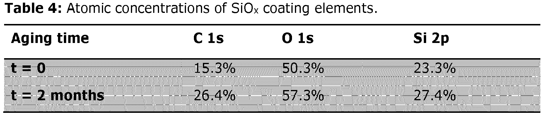
- The transparent element used in example 1 was PMMA. The dimensions and rougness factor of the nanotextured surface with and without SiOx coating is shown in table 3. The nanotextured surface was obtained by block copolymer (BPC) in situ nanolithography from the self-assembly of SD24, as described in the materials and methods section. The sub-diffraction limit length scale of the nanotexture rendered the surfaces perfectly transparent for visible light. The coating was a SiOx based coating deposited onto the nanotextured surface by plasma enhanced chemical vapor deposition (PECVD) as desribed in the material and methods section.
Table 3. Dimensions and roughness factors of nanotextured surface with and without SiOx coating and their associated uncertainties. d [nm] h [nm] a [nm] r a h/d a/d Nanotextured surface 55.1±1. 6 55±5 73.3±1.1 3.1±0.2 1.0±0.1 1.33±0.04 Nanotextured surface + SiOx coating 66.0±1. 4 66±5 74.0±2.1 3.9±0.3 1.00±0.08 1.12±0.04 - Other transparent hydrophilic coatings may have the same effect as the SiOx coating. Plasma treatment is another widely applied method to achieve wetting by adding or activating surface functional groups. Plasmas of Ar, He, O2, N2 and air, and exposures to UV light have been tested mostly on polymeric materials and a hydrophilic behavior is achieved through this treatment.
- Nanotexturing of PMMA: Polystyrene - b - polydimethylsiloxane PS - PDMS block - copolymer (SD24) with a number - average molecular weight (Mn) of 172 kg / mol and a very narrow polydispersity index of PDI ≤ 1.06 (TableS1) was used for the nanolithography processing. SD24 was first dissolved in cyclohexane (0.25 wt %) and then spin - cast (LabSpin6, SUSS) on a single crystalline silicon (Si) wafer (directly from the shelf, without further cleaning) at a spinning speed of 2000 rpm, yielding a 28 nm thick film. SD24 was then subjected to the solvent annealing in methylcyclohexane at room temperature with the sample closed in a glass jar in the presence of the solvent vapor for 160 min, creating densely packed PS cylinders in a hexagonal array. Subsequent mask fabrication was conducted in an Advanced Silicon Etcher (STS MESC Multiplex ICP serial no. 30343). For pretreatment, SF6 plasma was applied for 15 s (20 sccm SF6, 20 mTorr, 50 W of coil power and 0 W of platen power) to remove the PDMS residual layer created on a top of the annealed surface and subsequent O2 plasma etching for 11 s (10 sccm O2, 5 mTorr, 200 W coil power and 20 W of platen power) to remove PS blocks and oxidize PDMS blocks simultaneously, resulting in a hard silica mask of hexagonally orientated holes with high selectivity. Pattern transfer to the silicon was performed by reactive ion etching in ICP Metal Etch (SPTS serial no. MP0637) through the first breakthrough step of the SF6 plasma for 35 s (20 sccm SF6, 3 mTorr, 100 W of coil power and 10 W of platen power) and following Cl2 etching for 20 s (20 sccm Cl2, 3 mTorr, 300 W of coil power and 40 W of coil power) creating shallow holes. Nanopillars were fabricated through initial deposition of 30 nm Al2O3 layer on a patterned substrate by ALD, working as an etching mask for a following Cl2 etching. ALD deposition was performed in Picosun ALD (model R200), using alternating exposures to trimethylaluminium (97 %, Aldrich) and deionized water H2O at 200° C for 300 cycles with N2 gas purge steps in between. The exposures and purge times for both precursors used in this study were 0.2 and 25 s, respectively. Adjustment of Cl2 etching time to 210 s (20 sccm Cl2, 3 mTorr, 300 W of coil power and 40 W of coil power) allowed for defined tuning of nanotexture aspect ratio to equal one. The nanostructured silicon master was then sputter coated with a ∼ 85 nm NiV thin film (Custom System, Kurt J. Lesker) which acted as a seed layer for subsequent Ni electroplating (Microform 200, Technotrans) of an inverted relief polarity metal mold with a thickness of 300 µm. The entire Si wafer, bonded to the mold, was removed by dissolving in a 10 M KOH (Sigma - Aldrich) bath at 80°C. Before injection molding, the nickel insert was coated with a perfluorodecyltrichlorosilane (FDTS) self-assembled monolayer (MVD100E, Applied Microstructures Inc) which worked as anti-stiction layer. Polymethyl methacrylate (PMMA, IG840, LG MMA Corporation, Korea) discs (50 mm diameter, 2 mm thick) were injection molded using an industrial injection molding machine (Victory 45, Engel, Austria) facilitated with the structured nickel mold. A variothermal molding process was employed with injection pressure 1000 bar, holding pressure 1200 bar and a melt temperature 250° C. After replication, part of the flat and nanostructured PMMA surfaces were treated in a low - pressure argon plasma (Atto Plasma Cleaner, Diener Electronic) with conditions: 5 W, 60 Pa for 2 - 78 s.
- Silica based (SiO x ) coating: of PMMA surfaces was done by plasma enhanced chemical vapor deposition (PECVD). The deposition process was carried out in a custom build RF - powered capacitive coupled plasma reactor with a stainless steel reactor chamber, and a parallel plate electrode configuration where the sample holder was the ground bottom electrode, also described by Moreno-Couranjou et al. For the SiOx coating, the plasma was fed with a hexamethyldisiloxane HDMSO/O2 mixture with monomer and oxygen flow rates at 2 sccm and 150 sccm, respectively. The layer thickness was controlled by the deposition time. Hence, the process was conducted at the power of 300 W and pressure of 300 mTorr for 48 s, resulting in the ∼11 nm thick coating on both flat and nanotextured PMMA.
- Condensation experiment: Condensation experiments were carried out in a custom built environmental chamber of 5 x 10 x 10 cm3 dimensions, equipped with a thermoelectric cooler (gSKIN, XM 27 9C, Sibalco AG, Switzerland) enabling adjustment of the substrate temperature, a copper plate working as a sample holder, and a temperature probe clamped between those two. The backside of the transparent PMMA sample was made anti-reflective using a black permanent marker. The sample was attached to the copper plate using thermal paste, and the chamber was closed. Using a LabVIEW programmed PID controller, the temperature was set to 5° C and stabilized for 75 s. Additional 8.75 min of stabilization was applied to assure the stabilization of the polymer sample. The relative humidity was continuously probed inside the chamber using a resistive hygrometer. The humidity of the vapor flow was set by choosing the mixing ratio between pure nitrogen and saturated DI water vapor prior to the chamber entrance. Diffusers were placed at both chamber inlet and outlet to remove any possible jet streams. Throughout the temperature stabilization time, 8 L/min of nitrogen was continuously run through the chamber to keep the relative humidity at 3 % and avoid any premature condensation. After temperature stabilization, 2 L/min of DI water saturated vapor was introduced into the chamber and after 5 seconds the 8 L/min of nitrogen was shut off. This caused a sudden increase in the temperature and humidity. The chamber humidity was approaching complete saturation in an exponential manner on a characteristic time scale of 36 s. Images of the condensation process were taking throughout 25 minutes of an experiment in time intervals of 3, 15 and 60 s using a Zeiss AXIO ZOOM.V16 Optical Microscope. The condensation procedure was performed one to two times on flat surfaces, and two to three times on the BCP surfaces.
- Measurement of contact angles: Contact angles were measured using an optical tensiometer (Attension Theta optical tensiometer, Biolin Scientific Holding AB, Sweden) with a high - speed camera (3000 fps, MotionXtra N3, IDT, USA) by the sessile drop method in a static mode. Shapes of droplets were fitted by the Young - Laplace fitting method (Attention Theta software, version 4.2). For all contact angle measurements, droplets of 6.5 µl volume were used. The baseline was determined using an auto baseline function in the Attention Theta software. For each sample, three measurements were made at different spots of the sample and mean values with standard deviations were calculated. Contact angles of the wetting samples were made on timescales much shorter than those associated with the hemiwicking flow.
-
- 1
- transparent element
- 2
- anti-fogging surface
- 3
- nanotextured structure in or on surface of transparent element
- 4
- pillar
- 5
- average pillar equivalent diameter
- 6
- average pillar height
- 7
- average center-center inter-pillar pitch size
- 8
- optically transparent hydrophilic coating or layer
- 9
- plasma treatment
- 10
- hexagonal array
- 11
- Young's contact angle
- 12
- inter-pillar space
Claims (14)
- A transparent element (1) comprising at least one anti-fogging surface (2) with a hydrophilic surface chemistry and a Young's contact angle (11) of less than 55 degrees, wherein the anti-fogging surface (2) comprise a nanotextured structure (3) on and/or in the transparent element (1), the nanotextured structure (3) comprising a dense hexagonal array (10) of pillars (4), wherein∘ the average pillar equivalent diameter (5) is in the range of 25-175 nm;∘ the average pillar height (6) to average pillar equivalent diameter (5) ratio is in the range of 2:1 and 1:2, preferably in the range of 1:0.9 and 1:1.1;∘ the average center-center inter-pillar pitch size (7) is in the range of 30-180 nm;∘ the inter-pillar space (12), defined as the average center-center inter-pillar pitch size (7) minus the average pillar equivalent diameter (5), is in the range of 5-20 nm and less than half of the average pillar equivalent diameter (5); and∘ the surface fraction is between 40-85%
- A transparent element (1) according to claim 1, wherein the nanotextured surface is coated by an optically transparent layer (8) of siliciumoxide or metal such as tungsten (W), titanium (Ti) or chromium (Cr).
- A transparent element (1) according to claim 1 or 2, wherein the nanotextured surface have received plasma treatment (9) with Ar, O2 or N2 plasma.
- A transparent element (1) according to any of the preceding claims, wherein the thickness of the transparent siliciumoxide or metal layer (8) is between 5-20 nm, such as between 10-20 nm, such as between 10-15 nm.
- A transparent element (1) according to any of the preceding claims, wherein the anti-fogging surface have a ratio of the actual surface area to the projected surface area between 2.5-5.5.
- A transparent element (1) according to any of the preceding claims, wherein the transparent element essentially consist of glass or plastic, such as thermoplastic.
- A transparent element (1) according to any of the preceding claims, wherein the transparent element essentially consist of poly(methylmethacrylate).
- A transparent element (1) according to any of the preceding claims, wherein the transparent element is used in or as windows, lenses, glasses, mirrors, goggles, wind shields, endoscopy devices, photovoltaic devices, fresnel optical elements, instrument panels or screens, optical user-interfaces or lighting devices.
- A method for providing a transparent element (1) comprising at least one anti-fogging surface (2), the method comprising- providing a transparent element (1);- providing a nanotextured surface (3) comprising a dense hexagonal array of pillars (4), wherein∘ the average pillar equivalent diameter (5) is in the range of 25-175 nm;∘ the average pillar height (6) to average pillar equivalent diameter (5) ratio is in the range of 2:1 and 1:2, preferably in the range of 1:0.9 and 1:1.1;∘ the average center-center inter-pillar pitch size (7) is in the range of 30-180 nm;∘ the interpillar space (12), defined as the average center-center inter-pillar pitch size (7) minus the average pillar equivalent diameter (5) is in the range of 5-20 nm and less than half of the average pillar equivalent diameter (d); and∘ the surface fraction is between 40-85%- surface treating the nanotextured surface
- A method for providing a transparent element (1) according to claim 9, wherein the surface treatment comprise coating the nanotextured surface with a optically transparent layer (8) of siliciumoxide or metal, such as tungsten (W), titanium (Ti), or chromium (Cr).
- A method for providing a transparent element (1) according to claims 9 or 10, wherein the surface treatment comprise plasma treatment (9) with Ar, O2 or N2 plasma.
- A method for providing a transparent element (1) according to any of claims 9-11, wherein the nanotextured structure (3) is provided by in situ block-copolymer nanolithography, electron-beam lithography, extreme UV-lithography, or x-ray lithography.
- A method for providing a transparent element (1) according to any of claims 9-12, wherein the nanotextured structure (3) is coated by the plasma enhanced chemical vapor deposition (PECVD) method or the sputtering method.
- A method of providing a transparent element (1) according to any of claims 9-13, wherein the transparent element (1), after surface treatment, is stored in vacuum or an inert atmosphere, such as an atmosphere of N2, until use.
Priority Applications (1)
| Application Number | Priority Date | Filing Date | Title |
|---|---|---|---|
| EP18150811.0A EP3508889A1 (en) | 2018-01-09 | 2018-01-09 | Anti-fogging transparent surface |
Applications Claiming Priority (1)
| Application Number | Priority Date | Filing Date | Title |
|---|---|---|---|
| EP18150811.0A EP3508889A1 (en) | 2018-01-09 | 2018-01-09 | Anti-fogging transparent surface |
Publications (1)
| Publication Number | Publication Date |
|---|---|
| EP3508889A1 true EP3508889A1 (en) | 2019-07-10 |
Family
ID=61022109
Family Applications (1)
| Application Number | Title | Priority Date | Filing Date |
|---|---|---|---|
| EP18150811.0A Withdrawn EP3508889A1 (en) | 2018-01-09 | 2018-01-09 | Anti-fogging transparent surface |
Country Status (1)
| Country | Link |
|---|---|
| EP (1) | EP3508889A1 (en) |
Cited By (2)
| Publication number | Priority date | Publication date | Assignee | Title |
|---|---|---|---|---|
| EP4382870A1 (en) | 2022-12-08 | 2024-06-12 | Kaunas University of Technology | Anti-fogging incremental scales for optical encoders and fabrication method thereof |
| EP4459237A1 (en) | 2023-05-05 | 2024-11-06 | Kaunas University of Technology | Non-fogging optical scales and scanning reticles coated by hydrophilic diamond-like carbon films |
Citations (4)
| Publication number | Priority date | Publication date | Assignee | Title |
|---|---|---|---|---|
| WO2012020295A1 (en) * | 2010-08-09 | 2012-02-16 | 6/6Università Degli Studi Di Bari | Optical elements having long-lasting hydrophilic and anti-fog properties and method for their preparation |
| EP2693238A1 (en) * | 2011-03-31 | 2014-02-05 | Dexerials Corporation | Optical element, display device, and input device |
| EP3165358A1 (en) * | 2014-07-23 | 2017-05-10 | Dexerials Corporation | Transparent film for face protective shield |
| EP3176613A1 (en) * | 2014-07-30 | 2017-06-07 | Dexerials Corporation | Transparent laminate |
-
2018
- 2018-01-09 EP EP18150811.0A patent/EP3508889A1/en not_active Withdrawn
Patent Citations (4)
| Publication number | Priority date | Publication date | Assignee | Title |
|---|---|---|---|---|
| WO2012020295A1 (en) * | 2010-08-09 | 2012-02-16 | 6/6Università Degli Studi Di Bari | Optical elements having long-lasting hydrophilic and anti-fog properties and method for their preparation |
| EP2693238A1 (en) * | 2011-03-31 | 2014-02-05 | Dexerials Corporation | Optical element, display device, and input device |
| EP3165358A1 (en) * | 2014-07-23 | 2017-05-10 | Dexerials Corporation | Transparent film for face protective shield |
| EP3176613A1 (en) * | 2014-07-30 | 2017-06-07 | Dexerials Corporation | Transparent laminate |
Non-Patent Citations (2)
| Title |
|---|
| DESROUSSEAUX C ET AL: "Fabrication of acrylonitrile-butadiene-styrene nanostructures with anodic alumina oxide templates, characterization and biofilm development test for staphylococcus epidermidis", 20150818, 18 August 2015 (2015-08-18), pages 1 - 21, XP002763994, DOI: 10.1371/JOURNAL.PONE.0135632 * |
| FIEDLER JÖRG ET AL: "The effect of substrate surface nanotopography on the behavior of multipotnent mesenchymal stromal cells and osteoblasts", BIOMATERIALS, vol. 34, no. 35, 19 August 2013 (2013-08-19), pages 8851 - 8859, XP028699881, ISSN: 0142-9612, DOI: 10.1016/J.BIOMATERIALS.2013.08.010 * |
Cited By (2)
| Publication number | Priority date | Publication date | Assignee | Title |
|---|---|---|---|---|
| EP4382870A1 (en) | 2022-12-08 | 2024-06-12 | Kaunas University of Technology | Anti-fogging incremental scales for optical encoders and fabrication method thereof |
| EP4459237A1 (en) | 2023-05-05 | 2024-11-06 | Kaunas University of Technology | Non-fogging optical scales and scanning reticles coated by hydrophilic diamond-like carbon films |
Similar Documents
| Publication | Publication Date | Title |
|---|---|---|
| EP2117735B1 (en) | Article having a nanotextured surface with superhydrophobic properties | |
| EP2065736B1 (en) | Anti-reflection structure body, method of producing the same and method of producing optical member | |
| CA2260470C (en) | Structured surfaces having hydrophobic properties | |
| AU2013381844B2 (en) | Anti-fog nanotextured surfaces and articles containing the same | |
| EP2177558B1 (en) | Polymer microstructure with tilted micropillar array and method of fabricating the same | |
| Yilbas et al. | Wetting and other physical characteristics of polycarbonate surface textured using laser ablation | |
| CN106459459A (en) | Self-cleaning superhydrophobic polymer material for stain resistance | |
| CN102532576A (en) | Nanoporous coating and its manufacturing method | |
| WO2019008589A1 (en) | Micro-nano patterned anti-abrasive polymeric coatings and a method of production thereof | |
| Telecka et al. | Mapping the transition to superwetting state for nanotextured surfaces templated from block-copolymer self-assembly | |
| KR101954410B1 (en) | Method for preparing anti-reflection surface using plasma etching and substrate having anti-reflection surface | |
| JP6322294B2 (en) | Mold manufacturing method and antireflection film manufacturing method | |
| US20010026859A1 (en) | Functional films, their use, articles having the films and processes for producing these | |
| EP1417042B1 (en) | Method for producing a coated synthetic body | |
| US7759229B2 (en) | Charge-free method of forming nanostructures on a substrate | |
| JP2008545037A (en) | Low wetting hysteresis polysiloxane-based material and deposition method thereof | |
| JP5742098B2 (en) | Method for producing mold for production of antireflection film | |
| WO2017093840A1 (en) | Micron patterned silicone hard-coated polymer (shc-p) surfaces | |
| KR101617718B1 (en) | Fabrication method of superhydrophobic film and the superhydrophobic film thereby | |
| US20250277117A1 (en) | An amphiphobic coating and method of preparing an amphiphobic coating | |
| US20090294404A1 (en) | Process for controlling surface wettability | |
| US12091745B2 (en) | Three-dimensional nano-patterns | |
| EP4729587A1 (en) | Block copolymer, composition, and article using same | |
| CN117960524B (en) | Coatings, their preparation methods, and products including them | |
| JP2017007157A (en) | Substrate with a hydrophilic film and manufacturing method therefor |
Legal Events
| Date | Code | Title | Description |
|---|---|---|---|
| PUAI | Public reference made under article 153(3) epc to a published international application that has entered the european phase |
Free format text: ORIGINAL CODE: 0009012 |
|
| AK | Designated contracting states |
Kind code of ref document: A1 Designated state(s): AL AT BE BG CH CY CZ DE DK EE ES FI FR GB GR HR HU IE IS IT LI LT LU LV MC MK MT NL NO PL PT RO RS SE SI SK SM TR |
|
| AX | Request for extension of the european patent |
Extension state: BA ME |
|
| STAA | Information on the status of an ep patent application or granted ep patent |
Free format text: STATUS: THE APPLICATION IS DEEMED TO BE WITHDRAWN |
|
| 18D | Application deemed to be withdrawn |
Effective date: 20200111 |