EP3506513A1 - Charge pump having level-shifting mechanism - Google Patents
Charge pump having level-shifting mechanism Download PDFInfo
- Publication number
- EP3506513A1 EP3506513A1 EP18202442.2A EP18202442A EP3506513A1 EP 3506513 A1 EP3506513 A1 EP 3506513A1 EP 18202442 A EP18202442 A EP 18202442A EP 3506513 A1 EP3506513 A1 EP 3506513A1
- Authority
- EP
- European Patent Office
- Prior art keywords
- transistor
- capacitor
- charge pump
- coupled
- switch
- Prior art date
- Legal status (The legal status is an assumption and is not a legal conclusion. Google has not performed a legal analysis and makes no representation as to the accuracy of the status listed.)
- Granted
Links
Images





Classifications
-
- H—ELECTRICITY
- H03—ELECTRONIC CIRCUITRY
- H03L—AUTOMATIC CONTROL, STARTING, SYNCHRONISATION OR STABILISATION OF GENERATORS OF ELECTRONIC OSCILLATIONS OR PULSES
- H03L7/00—Automatic control of frequency or phase; Synchronisation
- H03L7/06—Automatic control of frequency or phase; Synchronisation using a reference signal applied to a frequency- or phase-locked loop
- H03L7/08—Details of the phase-locked loop
- H03L7/085—Details of the phase-locked loop concerning mainly the frequency- or phase-detection arrangement including the filtering or amplification of its output signal
- H03L7/089—Details of the phase-locked loop concerning mainly the frequency- or phase-detection arrangement including the filtering or amplification of its output signal the phase or frequency detector generating up-down pulses
- H03L7/0891—Details of the phase-locked loop concerning mainly the frequency- or phase-detection arrangement including the filtering or amplification of its output signal the phase or frequency detector generating up-down pulses the up-down pulses controlling source and sink current generators, e.g. a charge pump
- H03L7/0895—Details of the current generators
-
- H—ELECTRICITY
- H02—GENERATION; CONVERSION OR DISTRIBUTION OF ELECTRIC POWER
- H02M—APPARATUS FOR CONVERSION BETWEEN AC AND AC, BETWEEN AC AND DC, OR BETWEEN DC AND DC, AND FOR USE WITH MAINS OR SIMILAR POWER SUPPLY SYSTEMS; CONVERSION OF DC OR AC INPUT POWER INTO SURGE OUTPUT POWER; CONTROL OR REGULATION THEREOF
- H02M3/00—Conversion of DC power input into DC power output
- H02M3/02—Conversion of DC power input into DC power output without intermediate conversion into AC
- H02M3/04—Conversion of DC power input into DC power output without intermediate conversion into AC by static converters
- H02M3/06—Conversion of DC power input into DC power output without intermediate conversion into AC by static converters using resistors or capacitors, e.g. potential divider
- H02M3/07—Conversion of DC power input into DC power output without intermediate conversion into AC by static converters using resistors or capacitors, e.g. potential divider using capacitors charged and discharged alternately by semiconductor devices with control electrode, e.g. charge pumps
-
- H—ELECTRICITY
- H03—ELECTRONIC CIRCUITRY
- H03L—AUTOMATIC CONTROL, STARTING, SYNCHRONISATION OR STABILISATION OF GENERATORS OF ELECTRONIC OSCILLATIONS OR PULSES
- H03L7/00—Automatic control of frequency or phase; Synchronisation
- H03L7/06—Automatic control of frequency or phase; Synchronisation using a reference signal applied to a frequency- or phase-locked loop
- H03L7/08—Details of the phase-locked loop
- H03L7/085—Details of the phase-locked loop concerning mainly the frequency- or phase-detection arrangement including the filtering or amplification of its output signal
-
- H—ELECTRICITY
- H03—ELECTRONIC CIRCUITRY
- H03L—AUTOMATIC CONTROL, STARTING, SYNCHRONISATION OR STABILISATION OF GENERATORS OF ELECTRONIC OSCILLATIONS OR PULSES
- H03L7/00—Automatic control of frequency or phase; Synchronisation
- H03L7/06—Automatic control of frequency or phase; Synchronisation using a reference signal applied to a frequency- or phase-locked loop
- H03L7/08—Details of the phase-locked loop
- H03L7/085—Details of the phase-locked loop concerning mainly the frequency- or phase-detection arrangement including the filtering or amplification of its output signal
- H03L7/089—Details of the phase-locked loop concerning mainly the frequency- or phase-detection arrangement including the filtering or amplification of its output signal the phase or frequency detector generating up-down pulses
- H03L7/0891—Details of the phase-locked loop concerning mainly the frequency- or phase-detection arrangement including the filtering or amplification of its output signal the phase or frequency detector generating up-down pulses the up-down pulses controlling source and sink current generators, e.g. a charge pump
- H03L7/0895—Details of the current generators
- H03L7/0896—Details of the current generators the current generators being controlled by differential up-down pulses
-
- H—ELECTRICITY
- H03—ELECTRONIC CIRCUITRY
- H03L—AUTOMATIC CONTROL, STARTING, SYNCHRONISATION OR STABILISATION OF GENERATORS OF ELECTRONIC OSCILLATIONS OR PULSES
- H03L7/00—Automatic control of frequency or phase; Synchronisation
- H03L7/06—Automatic control of frequency or phase; Synchronisation using a reference signal applied to a frequency- or phase-locked loop
- H03L7/08—Details of the phase-locked loop
- H03L7/099—Details of the phase-locked loop concerning mainly the controlled oscillator of the loop
Definitions
- a conventional charge pump generally includes two current sources for charging and discharging an output node to generate a suitable control voltage to a following voltage-controlled oscillator (VCO) to generate an output clock signal.
- the two current sources are generally implemented by a P-type transistor and an N-type transistor, respectively, and drain-to-source voltages of the P-type transistor or the N-type transistor are generally designed larger to have lower noise.
- the larger drain-to-source voltages mean that the control voltage has a narrow range. If the charge pump is applied in a low-voltage application (i.e. low supply voltage), this narrow headroom issue may become worse, and the functions and noise of the charge pump may be worsened.
- a charge pump includes a pull-up circuit for selectively providing charges to an output terminal of the charge pump, and the pull-up circuit comprises a transistor, a capacitor and a switched-capacitor circuit, wherein the capacitor is coupled to an electrode of the transistor, and the switched-capacitor circuit is coupled between a supply voltage and another electrode of the transistor.
- the switched-capacitor circuit is configured to boost a voltage of the other electrode of the transistor to charge the capacitor via the transistor, then the capacitor and the output terminal of the charge pump are under a charge distribution operation.
- a phase-locked loop includes a phase detector, a charge pump, a voltage-controlled oscillator and a frequency divider.
- the phase detector is configured to receive an input signal and a feedback signal to generate a detection result
- the charge pump is configured to generate a control signal according to the detection result
- the voltage-controlled oscillator is configured to generate an output clock signal according to the control signal
- the frequency divider is configured to frequency-divide the output clock signal to generate the feedback signal.
- the charge pump includes a pull-up circuit for selectively providing charges to an output terminal of the charge pump
- the pull-up circuit comprises a transistor, a capacitor and a switched-capacitor circuit, wherein the capacitor is coupled to an electrode of the transistor, and the switched-capacitor circuit is coupled between a supply voltage and another electrode of the transistor.
- the switched-capacitor circuit is configured to boost a voltage of the other electrode of the transistor to charge the capacitor via the transistor, then the capacitor and the output terminal of the charge pump are under a charge distribution operation.
- a charge pump includes a pull-up circuit for selectively providing charges to an output terminal of the charge pump, and the pull-up circuit comprises a transistor, a capacitor, a switched-capacitor circuit and a switch, wherein the capacitor is coupled to an electrode of the transistor, the switched-capacitor circuit is coupled between a supply voltage and another electrode of the transistor, and the switch is coupled between the first electrode of the first transistor and the output terminal of the charge pump.
- the pull-up circuit operates in a first phase
- the switched-capacitor circuit is controlled to charge the first capacitor via the first transistor, and the switch is controlled to disconnect the first electrode of the first transistor from the output terminal of the charge pump.
- the pull-up circuit operates in a second phase, the switched-capacitor circuit is controlled to be disconnected from the second electrode of the first transistor, and the switch is controlled to connect the first electrode of the first transistor to the output terminal of the charge pump.
- FIG. 1 is a diagram illustrating a charge pump 100 according to one embodiment of the present invention.
- the charge pump 100 comprises a pull-up circuit 110 and a pull-down circuit 120.
- the pull-up circuit 110 is configured to receive a clock signal CLK to selectively charge an output terminal Nout of the charge pump 100
- the pull-down circuit 120 is configured to receive a control signal DN to selectively discharge the output terminal Nout of the charge pump 100, so as to generate a control voltage Vc to a following circuit such as a VCO.
- FIG. 2 shows the detailed structures of the charge pump 100 according to one embodiment of the present invention.
- the pull-up circuit 100 comprises two P-type transistors P1 and P2, one resistor R1 coupled between a drain electrode of the P-type transistor P2 and a ground voltage, a switched-capacitor circuit 112, a capacitor C1 and a switch SW3, where a gate electrode of the P-type transistors P1 is coupled to a gate electrode of the P-type transistors P2, the switched-capacitor circuit 112 is coupled between a supply voltage VDD and a source electrode of the P-type transistor P1, the capacitor C1 is coupled between a drain electrode of the P-type transistor P1 and the ground voltage, and the switch SW3 is coupled between the capacitor C1 and the output terminal Nout.
- the switched-capacitor circuit 112 comprises two switches SW1 and SW2, and a capacitor C2, where a first node N1 of the capacitor C2 is connected to the clock signal CLK, the switch SW1 is coupled between the supply voltage VDD and a second node N2 of the capacitor C2, and the switch SW2 is coupled between the source electrode of the P-type transistor P1 and the second node N2 of the capacitor C2.
- the switch SW2 is controlled by the clock signal CLK
- the switches SW1 and SW3 are controlled by an inverted clock signal CLKB.
- the pull-down circuit 120 comprises a current source 122, a capacitor C3 and a switch SW4, where one node of the capacitor C3 is coupled to the clock signal CLK, a current source 122 controlled by the control signal DN is coupled to the other node of the capacitor C3, and the switch SW4 controlled by the inverted clock signal CLKB is coupled between the other node of the capacitor C3 and the output terminal Nout.
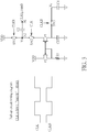
- FIG. 3 is a diagram illustrating a sample phase of the pull-up circuit 110 according to one embodiment of the present invention
- FIG. 4 is a diagram illustrating a hold phase of the pull-up circuit 110 according to one embodiment of the present invention.
- a level of the clock signal is low (e.g. ground voltage)
- the switch SW1 is controlled to connect the supply voltage VDD to the node N2
- the switch SW2 is controlled to disconnect the node N2 from the source electrode of the P-type transistor P1
- the switch SW3 is controlled to connect the capacitor C1 to the capacitor C4.
- the capacitor C1 is connected to the capacitor C4 to perform a charge re-distribution, that is the charges at the capacitor C1 may flow to the capacitor C4 until their voltages are equal.
- the charge re-distribution path i.e. the capacitor C1 is not electrically connected to any supply voltage VDD, so charge re-distribution path and the control voltage Vc will have lower noise because the supply voltage VDD generally have noise and spur.
- FIG. 5 shows a voltage Vs of the node N2 according to one embodiment of the present invention.
- the voltage Vs of the node N2 is equal to VDD because the switch SW1 is controlled to connect the supply voltage VDD to the node N2.
- the voltage Vs is immediately boosted to "2*VDD" because the node N1 has the voltage VDD and the cross-voltage of the capacitor C2 cannot immediately change. Then, the node N2 charges the capacitor C1 via the switch SW2 and the P-type transistor P1 until the voltage Vs is equal to VDD. In the hold phase of the pull-up circuit 110, because the voltage Vs of the node N2 is boosted to the "2*VDD" at the beginning of the hold phase, the charges can completely transported to capacitor C1 due to the high voltage Vs.
- the P-type transistors P1 and P2 form a current mirror, and the P-type transistor P2 is controlled to be barely off (i.e. a gate-to-source voltage of the P-type transistor P2 is close to a threshold voltage), so the voltage Vs can be precisely controlled to have the voltage VDD at the end of the hold phase. Furthermore, because the charge generation at the node N2 is not dependent on any transistor, so the charge generation will not be influenced by the threshold voltage or other properties of the transistor, and the charge generation virtually consumes zero headroom since the Vdsat (i.e. a difference between a gate-source voltage and a threshold voltage) of the transistor P1 is virtually zero.
- FIG. 6 is a diagram illustrating a sample phase of the pull-down circuit 120 according to one embodiment of the present invention
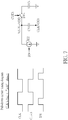
- FIG. 7 is a diagram illustrating a hold phase of the pull-down circuit 120 according to one embodiment of the present invention.
- the level of the clock signal is low (e.g. ground voltage)
- the current source 122 is disabled, and the switch SW4 is controlled to connect the capacitor C3 to the capacitor C4.
- the capacitor C3 is connected to the capacitor C4 to perform the charge re-distribution, that is the charges at the capacitor C3 may flow to the capacitor C4 until their voltages are equal.
- the charge re-distribution path i.e. the capacitor C3
- the control voltage Vc will have lower noise because the supply voltage VDD generally have noise and spur.
- the switch SW4 is controlled to disconnect the capacitor C3 from the capacitor C4.
- the voltage Vs' of the upper node of the capacitor C3 is equal to "Vc+VDD", wherein the value of the control voltage Vc corresponds to the previous sample phase. Therefore, when the clock signal CLK goes high and the pull-down circuit 120 enters the hold phase, the voltage Vs' is immediately boosted to "Vc+VDD" because the lower node of the capacitor C3 has the voltage VDD and the cross-voltage of the capacitor C3 cannot immediately change.
- the current source 122 may have large headroom and the noise of the current source 122 can be effectively reduced, and the control voltage Vc may have larger range.
- the control voltage Vc has a larger control range (e.g. ground to VDD), and the charge generation of the pull-up circuit 110 virtually consumes zero headroom, and more headroom can be reserved for the current source 122 of the pull-down circuit 120 to reduce the noise.
- the charge generation of the pull-up circuit 110 is based on the current-mirror-like topology, the voltage supply's noise cab be blocked.
- the charge pump 100 can be applied in a phase-locked loop 800 as shown in FIG. 8 .
- the phase-locked loop 800 comprises a phase-frequency detector 810, the charge pump 100, a loop filter 830, a VCO 840 and a frequency divider 850.
- the phase-frequency detector 810 receives an input signal (reference clock signal) Vin and a feedback signal VFB to generate a detection result
- the charge pump 100 generates the control voltage Vc according to the detection result
- the loop filter 830 filters the control voltage Vc to generate a filtered control voltage Vc'
- the VCO 840 generates an output clock signal CK_OUT according to the filtered control voltage Vc'
- the frequency divider 850 frequency-divides the output clock signal CK_OUT to generate the feedback signal VFB.
- the present invention may also be defined by means of the following numbered clauses.
Landscapes
- Engineering & Computer Science (AREA)
- Power Engineering (AREA)
- Stabilization Of Oscillater, Synchronisation, Frequency Synthesizers (AREA)
Abstract
Description
- This application claims the priority of
US Provisional Application No. 62/610,315, filed on December 26th, 2017 - A conventional charge pump generally includes two current sources for charging and discharging an output node to generate a suitable control voltage to a following voltage-controlled oscillator (VCO) to generate an output clock signal. The two current sources are generally implemented by a P-type transistor and an N-type transistor, respectively, and drain-to-source voltages of the P-type transistor or the N-type transistor are generally designed larger to have lower noise. However, the larger drain-to-source voltages mean that the control voltage has a narrow range. If the charge pump is applied in a low-voltage application (i.e. low supply voltage), this narrow headroom issue may become worse, and the functions and noise of the charge pump may be worsened.
- It is therefore an objective of the present invention to provide a charge pump which allows a large range for the control voltage and has low noise, to solve the above-mentioned problems.
- According to one embodiment of the present invention, a charge pump includes a pull-up circuit for selectively providing charges to an output terminal of the charge pump, and the pull-up circuit comprises a transistor, a capacitor and a switched-capacitor circuit, wherein the capacitor is coupled to an electrode of the transistor, and the switched-capacitor circuit is coupled between a supply voltage and another electrode of the transistor. The switched-capacitor circuit is configured to boost a voltage of the other electrode of the transistor to charge the capacitor via the transistor, then the capacitor and the output terminal of the charge pump are under a charge distribution operation.
- According to another embodiment of the present invention, a phase-locked loop includes a phase detector, a charge pump, a voltage-controlled oscillator and a frequency divider. In the operations of the phase-locked loop, the phase detector is configured to receive an input signal and a feedback signal to generate a detection result, the charge pump is configured to generate a control signal according to the detection result, the voltage-controlled oscillator is configured to generate an output clock signal according to the control signal, and the frequency divider is configured to frequency-divide the output clock signal to generate the feedback signal. In one embodiment, the charge pump includes a pull-up circuit for selectively providing charges to an output terminal of the charge pump, and the pull-up circuit comprises a transistor, a capacitor and a switched-capacitor circuit, wherein the capacitor is coupled to an electrode of the transistor, and the switched-capacitor circuit is coupled between a supply voltage and another electrode of the transistor. The switched-capacitor circuit is configured to boost a voltage of the other electrode of the transistor to charge the capacitor via the transistor, then the capacitor and the output terminal of the charge pump are under a charge distribution operation.
- According to another embodiment of the present invention, a charge pump includes a pull-up circuit for selectively providing charges to an output terminal of the charge pump, and the pull-up circuit comprises a transistor, a capacitor, a switched-capacitor circuit and a switch, wherein the capacitor is coupled to an electrode of the transistor, the switched-capacitor circuit is coupled between a supply voltage and another electrode of the transistor, and the switch is coupled between the first electrode of the first transistor and the output terminal of the charge pump. When the pull-up circuit operates in a first phase, the switched-capacitor circuit is controlled to charge the first capacitor via the first transistor, and the switch is controlled to disconnect the first electrode of the first transistor from the output terminal of the charge pump. When the pull-up circuit operates in a second phase, the switched-capacitor circuit is controlled to be disconnected from the second electrode of the first transistor, and the switch is controlled to connect the first electrode of the first transistor to the output terminal of the charge pump.
- These and other objectives of the present invention will no doubt become obvious to those of ordinary skill in the art after reading the following detailed description of the preferred embodiment that is illustrated in the various figures and drawings.
-
-
FIG. 1 is a diagram illustrating a charge pump according to one embodiment of the present invention. -
FIG. 2 shows the detailed structures of the charge pump according to one embodiment of the present invention. -
FIG. 3 is a diagram illustrating a sample phase of the pull-up circuit according to one embodiment of the present invention. -
FIG. 4 is a diagram illustrating a hold phase of the pull-up circuit according to one embodiment of the present invention. -
FIG. 5 shows a voltage of the node N2 according to one embodiment of the present invention. -
FIG. 6 is a diagram illustrating a sample phase of the pull-down circuit according to one embodiment of the present invention. -
FIG. 7 is a diagram illustrating a hold phase of the pull-down circuit according to one embodiment of the present invention. -
FIG. 8 is a diagram illustrating a phase-locked loop according to one embodiment of the present invention. - Certain terms are used throughout the following description and claims to refer to particular system components. As one skilled in the art will appreciate, manufacturers may refer to a component by different names. This document does not intend to distinguish between components that differ in name but not function. In the following discussion and in the claims, the terms "including" and "comprising" are used in an open-ended fashion, and thus should be interpreted to mean "including, but not limited to ...". The terms "couple" and "couples" are intended to mean either an indirect or a direct electrical connection. Thus, if a first device couples to a second device, that connection may be through a direct electrical connection, or through an indirect electrical connection via other devices and connections.
-
FIG. 1 is a diagram illustrating acharge pump 100 according to one embodiment of the present invention. As shown inFIG. 1 , thecharge pump 100 comprises a pull-up circuit 110 and a pull-down circuit 120. In the operations of thecharge pump 100, the pull-up circuit 110 is configured to receive a clock signal CLK to selectively charge an output terminal Nout of thecharge pump 100, and the pull-down circuit 120 is configured to receive a control signal DN to selectively discharge the output terminal Nout of thecharge pump 100, so as to generate a control voltage Vc to a following circuit such as a VCO. -
FIG. 2 shows the detailed structures of thecharge pump 100 according to one embodiment of the present invention. As shown inFIG. 2 , the pull-up circuit 100 comprises two P-type transistors P1 and P2, one resistor R1 coupled between a drain electrode of the P-type transistor P2 and a ground voltage, a switched-capacitor circuit 112, a capacitor C1 and a switch SW3, where a gate electrode of the P-type transistors P1 is coupled to a gate electrode of the P-type transistors P2, the switched-capacitor circuit 112 is coupled between a supply voltage VDD and a source electrode of the P-type transistor P1, the capacitor C1 is coupled between a drain electrode of the P-type transistor P1 and the ground voltage, and the switch SW3 is coupled between the capacitor C1 and the output terminal Nout. In addition, the switched-capacitor circuit 112 comprises two switches SW1 and SW2, and a capacitor C2, where a first node N1 of the capacitor C2 is connected to the clock signal CLK, the switch SW1 is coupled between the supply voltage VDD and a second node N2 of the capacitor C2, and the switch SW2 is coupled between the source electrode of the P-type transistor P1 and the second node N2 of the capacitor C2. In the embodiment shown inFIG. 2 , the switch SW2 is controlled by the clock signal CLK, and the switches SW1 and SW3 are controlled by an inverted clock signal CLKB. - The pull-
down circuit 120 comprises acurrent source 122, a capacitor C3 and a switch SW4, where one node of the capacitor C3 is coupled to the clock signal CLK, acurrent source 122 controlled by the control signal DN is coupled to the other node of the capacitor C3, and the switch SW4 controlled by the inverted clock signal CLKB is coupled between the other node of the capacitor C3 and the output terminal Nout. -
FIG. 3 is a diagram illustrating a sample phase of the pull-up circuit 110 according to one embodiment of the present invention, andFIG. 4 is a diagram illustrating a hold phase of the pull-up circuit 110 according to one embodiment of the present invention. As shown inFIG. 3 , when a level of the clock signal is low (e.g. ground voltage), the switch SW1 is controlled to connect the supply voltage VDD to the node N2, the switch SW2 is controlled to disconnect the node N2 from the source electrode of the P-type transistor P1, and the switch SW3 is controlled to connect the capacitor C1 to the capacitor C4. In the sample phase shown inFIG. 3 , the capacitor C1 is connected to the capacitor C4 to perform a charge re-distribution, that is the charges at the capacitor C1 may flow to the capacitor C4 until their voltages are equal. In addition, in the sample phase of the pull-up circuit 110, the charge re-distribution path (i.e. the capacitor C1) is not electrically connected to any supply voltage VDD, so charge re-distribution path and the control voltage Vc will have lower noise because the supply voltage VDD generally have noise and spur. - When the level of the clock signal CLK is high (e.g. VDD), the pull-
up circuit 110 is in the hold phase, and the switch SW1 is controlled to disconnect the supply voltage VDD from the node N2, the switch SW2 is controlled to connect the node N2 to the source electrode of the P-type transistor P1, and the switch SW3 is controlled to disconnect the capacitor C1 from the capacitor C4. Refer toFIG. 4 andFIG. 5 together,FIG. 5 shows a voltage Vs of the node N2 according to one embodiment of the present invention. In the sample period shown inFIG. 3 , the voltage Vs of the node N2 is equal to VDD because the switch SW1 is controlled to connect the supply voltage VDD to the node N2. Therefore, when the clock signal CLK goes high and the pull-up circuit 110 enters the hold phase shown inFIG. 4 , the voltage Vs is immediately boosted to "2*VDD" because the node N1 has the voltage VDD and the cross-voltage of the capacitor C2 cannot immediately change. Then, the node N2 charges the capacitor C1 via the switch SW2 and the P-type transistor P1 until the voltage Vs is equal to VDD. In the hold phase of the pull-up circuit 110, because the voltage Vs of the node N2 is boosted to the "2*VDD" at the beginning of the hold phase, the charges can completely transported to capacitor C1 due to the high voltage Vs. In addition, the P-type transistors P1 and P2 form a current mirror, and the P-type transistor P2 is controlled to be barely off (i.e. a gate-to-source voltage of the P-type transistor P2 is close to a threshold voltage), so the voltage Vs can be precisely controlled to have the voltage VDD at the end of the hold phase. Furthermore, because the charge generation at the node N2 is not dependent on any transistor, so the charge generation will not be influenced by the threshold voltage or other properties of the transistor, and the charge generation virtually consumes zero headroom since the Vdsat (i.e. a difference between a gate-source voltage and a threshold voltage) of the transistor P1 is virtually zero. -
FIG. 6 is a diagram illustrating a sample phase of the pull-down circuit 120 according to one embodiment of the present invention, andFIG. 7 is a diagram illustrating a hold phase of the pull-down circuit 120 according to one embodiment of the present invention. As shown inFIG. 6 , when the level of the clock signal is low (e.g. ground voltage), thecurrent source 122 is disabled, and the switch SW4 is controlled to connect the capacitor C3 to the capacitor C4. In the sample phase shown inFIG. 6 , the capacitor C3 is connected to the capacitor C4 to perform the charge re-distribution, that is the charges at the capacitor C3 may flow to the capacitor C4 until their voltages are equal. In addition, in the sample phase of the pull-down circuit 120, the charge re-distribution path (i.e. the capacitor C3) is not electrically connected to any supply voltage VDD, so charge re-distribution path and the control voltage Vc will have lower noise because the supply voltage VDD generally have noise and spur. - When the level of the clock signal is high (e.g. VDD), the pull-
down circuit 120 is in the hold phase, the switch SW4 is controlled to disconnect the capacitor C3 from the capacitor C4. In the hold phase shown inFIG. 7 , the voltage Vs' of the upper node of the capacitor C3 is equal to "Vc+VDD", wherein the value of the control voltage Vc corresponds to the previous sample phase. Therefore, when the clock signal CLK goes high and the pull-downcircuit 120 enters the hold phase, the voltage Vs' is immediately boosted to "Vc+VDD" because the lower node of the capacitor C3 has the voltage VDD and the cross-voltage of the capacitor C3 cannot immediately change. In the hold phase of the pull-down circuit 120, because the voltage Vs' of the upper node of the capacitor C3 is boosted to the "Vc+VDD", thecurrent source 122 may have large headroom and the noise of thecurrent source 122 can be effectively reduced, and the control voltage Vc may have larger range. - Briefly summarizing the embodiments shown in
FIG. 2-7 , because the pull-up circuit 110 and the pull-down circuit 120 employ the level-shifting techniques (e.g. the switched-capacitor circuit 112), the control voltage Vc has a larger control range (e.g. ground to VDD), and the charge generation of the pull-up circuit 110 virtually consumes zero headroom, and more headroom can be reserved for thecurrent source 122 of the pull-down circuit 120 to reduce the noise. In addition, because the charge generation of the pull-up circuit 110 is based on the current-mirror-like topology, the voltage supply's noise cab be blocked. - In one embodiment, the
charge pump 100 can be applied in a phase-lockedloop 800 as shown inFIG. 8 . InFIG. 8 , the phase-lockedloop 800 comprises a phase-frequency detector 810, thecharge pump 100, aloop filter 830, aVCO 840 and afrequency divider 850. In the operations of the phase-lockedloop 800, the phase-frequency detector 810 receives an input signal (reference clock signal) Vin and a feedback signal VFB to generate a detection result, thecharge pump 100 generates the control voltage Vc according to the detection result, theloop filter 830 filters the control voltage Vc to generate a filtered control voltage Vc', theVCO 840 generates an output clock signal CK_OUT according to the filtered control voltage Vc', and thefrequency divider 850 frequency-divides the output clock signal CK_OUT to generate the feedback signal VFB. - Those skilled in the art will readily observe that numerous modifications and alterations of the device and method may be made while retaining the teachings of the invention. Accordingly, the above disclosure should be construed as limited only by the metes and bounds of the appended claims.
- The present invention may also be defined by means of the following numbered clauses.
- 1. A charge pump, comprising:
- a pull-up circuit, for selectively providing charges to an output terminal of the charge pump, wherein the pull-up circuit comprises:
- a first transistor;
- a first capacitor, coupled to one electrode of the first transistor; and
- a switched-capacitor circuit, coupled between a supply voltage and another electrode of the transistor, for boosting a voltage of the other electrode of the first transistor to charge the first capacitor via the first transistor, then the first capacitor and the output terminal of the charge pump are under a charge distribution operation.
- a pull-up circuit, for selectively providing charges to an output terminal of the charge pump, wherein the pull-up circuit comprises:
- 2. The charge pump of clause 1, wherein when the capacitor and the output terminal of the charge pump are under the charge distribution operation, the capacitor is electrically disconnected from the supply voltage.
- 3. The charge pump of clause 1, wherein the first transistor is a P-type transistor, and the switched-capacitor circuit comprises:
- a second capacitor, wherein a first node of the second capacitor is coupled to a first clock signal;
- a first switch, coupled between the supply voltage and a second node of the second capacitor, wherein the first switch is controlled by a second clock signal to connect or disconnect the supply voltage to the second node of the second capacitor, wherein phases of the second clock signal and the first clock signal are inverted; and
- a second switch, coupled between second node of the second capacitor and a source electrode of the first transistor, wherein the second switch is controlled by the first clock signal to connect or disconnect the second capacitor to the source electrode of the first transistor.
- 4. The charge pump of clause 3, further comprising:
a third switch, coupled between a drain electrode of the first transistor and the output terminal of the charge pump, wherein the third switch is controlled by the second clock signal to connect or disconnect the drain electrode of the first transistor to the output terminal of the charge pump. - 5. The charge pump of clause 1, wherein the pull-up circuit further comprises:
- a second transistor, wherein a gate electrode of the second transistor is coupled to a gate electrode of the first transistor, and a first electrode of the second transistor is coupled to the supply voltage; and
- a resistor, coupled between a second electrode of the second transistor and a ground voltage, and the second electrode of the second transistor is also coupled to its gate electrode.
- 6. The charge pump of clause 5, wherein the first transistor and the second transistor are P-type transistors, and the second transistor is barely off for a normal state.
- 7. The charge pump of clause 1, further comprising:
a pull-down circuit, comprising:
a current source, coupled to the output terminal of the charge pump via a switch, for selectively discharges the output terminal of the charge pump. - 8. The charge pump of clause 7, wherein the pull-down circuit further comprises:
- a third capacitor, wherein a first node of the third capacitor is coupled to a first clock signal, and a second node of the third capacitor is coupled to the current source;
- wherein the switch is controlled by a second clock signal to connect or disconnect the current source to the output terminal of the charge pump, and the phases of the second clock signal and the first clock signal are inverted.
- 9. A phase-locked loop, comprising:
- a phase detector, for receiving an input signal and a feedback signal to generate a detection result;
- a charge pump, for generating a control signal according to the detection result, wherein the charge pump comprises:
a pull-up circuit, for selectively providing charges to an output terminal of the charge pump, wherein the pull-up circuit comprises:- a first transistor;
- a first capacitor, coupled to one electrode of the first transistor; and
- a switched-capacitor circuit, coupled between a supply voltage another electrode of the transistor, for boosting a voltage of the other electrode of the first transistor to charge the first capacitor via the first transistor, then the first capacitor and the output terminal of the charge pump are under a charge distribution operation; and
- a voltage-controlled oscillator, for generating an output clock signal according to the control signal; and
- a frequency divider, for frequency-dividing the output clock signal to generate the feedback signal.
- 10. The phase-locked loop of clause 9, wherein when the capacitor and the output terminal of the charge pump are under the charge distribution operation, the capacitor is electrically disconnected from the supply voltage.
- 11. The phase-locked loop of clause 9, wherein the first transistor is a P-type transistor, and the switched-capacitor circuit comprises:
- a second capacitor, wherein a first node of the second capacitor is coupled to a first clock signal;
- a first switch, coupled between the supply voltage and a second node of the second capacitor, wherein the first switch is controlled by a second clock signal to connect or disconnect the supply voltage to the second node of the second capacitor, wherein phases of the second clock signal and the first clock signal are inverted; and
- a second switch, coupled between the second node of the second capacitor and a source electrode of the first transistor, wherein the second switch is controlled by the first clock signal to connect or disconnect the second capacitor to the source electrode of the first transistor.
- 12. The phase-locked loop of clause 11, further comprising: a third switch, coupled between a drain electrode of the first transistor and the output terminal of the charge pump, wherein the third switch is controlled by the second clock signal to connect or disconnect the drain electrode of the first transistor to the output terminal of the charge pump.
- 13. The phase-locked loop of clause 9, wherein the pull-up circuit further comprises:
- a second transistor, wherein a gate electrode of the second transistor is coupled to a gate electrode of the first transistor, and a first electrode of the second transistor is coupled to the supply voltage; and
- a resistor, coupled between a second electrode of the second transistor and a ground voltage, and the second electrode of the second transistor is also coupled to its gate electrode.
- 14. The phase-locked loop of clause 13, wherein the first transistor and the second transistor are P-type transistors, and the second transistor is barely off for a normal state.
- 15. The phase-locked loop of clause 9, further comprising:
a pull-down circuit, comprising:
a current source, coupled to the output terminal of the charge pump via a switch, for selectively discharges the output terminal of the charge pump. - 16. The phase-locked loop of clause 15, wherein the pull-down circuit further comprises:
- a third capacitor, wherein a first node of the third capacitor is coupled to a first clock signal, and a second node of the third capacitor is coupled to the current source;
- wherein the switch is controlled by a second clock signal to connect or disconnect the current source to the output terminal of the charge pump, and the phases of the second clock signal and the first clock signal are inverted.
- 17. A charge pump, comprising:
a pull-up circuit, for selectively providing charges to an output terminal of the charge pump, wherein the pull-up circuit comprises:- a first transistor;
- a first capacitor, coupled to a first electrode of the first transistor; and
- a switched-capacitor circuit, coupled between a supply voltage and a second electrode of the transistor,
- a switch, coupled between the first electrode of the first transistor and the output terminal of the charge pump;
- wherein when the pull-up circuit operates in a first phase, the switched-capacitor circuit is controlled to charge the first capacitor via the first transistor, and the switch is controlled to disconnect the first electrode of the first transistor from the output terminal of the charge pump; and when the pull-up circuit operates in a second phase, the switched-capacitor circuit is controlled to be disconnected from the second electrode of the first transistor, and the switch is controlled to connect the first electrode of the first transistor to the output terminal of the charge pump.
- 18. The charge pump of clause 17, wherein the switch is a third switch, the first transistor is a P-type transistor, and the switched-capacitor circuit comprises:
- a second capacitor, wherein a first node of the second capacitor is coupled to a first clock signal;
- a first switch, coupled between the supply voltage and a second node of the second capacitor, wherein the first switch is controlled by a second clock signal to connect or disconnect the supply voltage to the second node of the second capacitor, wherein phases of the second clock signal and the first clock signal are inverted; and
- a second switch, coupled between second node of the second capacitor and a source electrode of the first transistor, wherein the second switch is controlled by the first clock signal to connect or disconnect the second capacitor to the source electrode of the first transistor.
- 19. The charge pump of clause 18, wherein the third switch is controlled by the second clock signal to connect or disconnect the drain electrode of the first transistor to the output terminal of the charge pump.
Claims (12)
- A charge pump (100), comprising:a pull-up circuit (110), for selectively providing charges to an output terminal of the charge pump (100), wherein the pull-up circuit (110) comprises:a first transistor;a first capacitor, coupled to one electrode of the first transistor; anda switched-capacitor circuit (112), coupled between a supply voltage and another electrode of the transistor, for boosting a voltage of the other electrode of the first transistor to charge the first capacitor via the first transistor, then the first capacitor and the output terminal of the charge pump (100) are under a charge distribution operation.
- The charge pump (100) of claim 1, wherein when the capacitor and the output terminal of the charge pump (100) are under the charge distribution operation, the capacitor is electrically disconnected from the supply voltage.
- The charge pump (100) of claim 1, wherein the first transistor is a P-type transistor, and the switched-capacitor circuit (112) comprises:a second capacitor, wherein a first node of the second capacitor is coupled to a first clock signal;a first switch, coupled between the supply voltage and a second node of the second capacitor, wherein the first switch is controlled by a second clock signal to connect or disconnect the supply voltage to the second node of the second capacitor, wherein phases of the second clock signal and the first clock signal are inverted; anda second switch, coupled between second node of the second capacitor and a source electrode of the first transistor, wherein the second switch is controlled by the first clock signal to connect or disconnect the second capacitor to the source electrode of the first transistor.
- The charge pump (100) of claim 3, further comprising:a third switch, coupled between a drain electrode of the first transistor and the output terminal of the charge pump (100), wherein the third switch is controlled by the second clock signal to connect or disconnect the drain electrode of the first transistor to the output terminal of the charge pump (100).
- The charge pump of (100) claim 1, wherein the pull-up circuit (110) further comprises:a second transistor, wherein a gate electrode of the second transistor is coupled to a gate electrode of the first transistor, and a first electrode of the second transistor is coupled to the supply voltage; anda resistor, coupled between a second electrode of the second transistor and a ground voltage, and the second electrode of the second transistor is also coupled to its gate electrode.
- The charge pump (100) of claim 5, wherein the first transistor and the second transistor are P-type transistors, and the second transistor is barely off for a normal state.
- The charge pump (100) of claim 1, further comprising:a pull-down circuit (120), comprising:a current source, coupled to the output terminal of the charge pump (100) via a switch, for selectively discharges the output terminal of the charge pump (100).
- The charge pump (100) of claim 7, wherein the pull-down circuit (120) further comprises:a third capacitor, wherein a first node of the third capacitor is coupled to a first clock signal, and a second node of the third capacitor is coupled to the current source;wherein the switch is controlled by a second clock signal to connect or disconnect the current source to the output terminal of the charge pump (100), and the phases of the second clock signal and the first clock signal are inverted.
- A phase-locked loop (800), comprising:a phase detector (810), for receiving an input signal and a feedback signal to generate a detection result;a charge pump (100) according to any one of claims 1 to 8, for generating a control signal according to the detection result;a voltage-controlled oscillator, for generating an output clock signal according to the control signal; anda frequency divider, for frequency-dividing the output clock signal to generate the feedback signal.
- A charge pump (100), comprising:a pull-up circuit (110), for selectively providing charges to an output terminal of the charge pump (100), wherein the pull-up circuit (110) comprises:a first transistor;a first capacitor, coupled to a first electrode of the first transistor; anda switched-capacitor circuit, coupled between a supply voltage and a second electrode of the transistor, a switch, coupled between the first electrode of the first transistor and the output terminal of the charge pump;wherein when the pull-up circuit (110) operates in a first phase, the switched-capacitor circuit is controlled to charge the first capacitor via the first transistor, and the switch is controlled to disconnect the first electrode of the first transistor from the output terminal of the charge pump (100) ; and when the pull-up circuit (120) operates in a second phase, the switched-capacitor circuit is controlled to be disconnected from the second electrode of the first transistor, and the switch is controlled to connect the first electrode of the first transistor to the output terminal of the charge pump (100).
- The charge pump (100) of claim 10, wherein the switch is a third switch, the first transistor is a P-type transistor, and the switched-capacitor circuit comprises:a second capacitor, wherein a first node of the second capacitor is coupled to a first clock signal;a first switch, coupled between the supply voltage and a second node of the second capacitor, wherein the first switch is controlled by a second clock signal to connect or disconnect the supply voltage to the second node of the second capacitor, wherein phases of the second clock signal and the first clock signal are inverted; anda second switch, coupled between second node of the second capacitor and a source electrode of the first transistor, wherein the second switch is controlled by the first clock signal to connect or disconnect the second capacitor to the source electrode of the first transistor.
- The charge pump (100) of claim 11, wherein the third switch is controlled by the second clock signal to connect or disconnect the drain electrode of the first transistor to the output terminal of the charge pump (100).
Applications Claiming Priority (2)
| Application Number | Priority Date | Filing Date | Title |
|---|---|---|---|
| US201762610315P | 2017-12-26 | 2017-12-26 | |
| US16/137,534 US10483845B2 (en) | 2017-12-26 | 2018-09-20 | Charge pump having level-shifting mechanism |
Publications (2)
| Publication Number | Publication Date |
|---|---|
| EP3506513A1 true EP3506513A1 (en) | 2019-07-03 |
| EP3506513B1 EP3506513B1 (en) | 2023-08-30 |
Family
ID=63998523
Family Applications (1)
| Application Number | Title | Priority Date | Filing Date |
|---|---|---|---|
| EP18202442.2A Active EP3506513B1 (en) | 2017-12-26 | 2018-10-24 | Charge pump having level-shifting mechanism |
Country Status (4)
| Country | Link |
|---|---|
| US (1) | US10483845B2 (en) |
| EP (1) | EP3506513B1 (en) |
| CN (1) | CN110011532B (en) |
| TW (1) | TWI690141B (en) |
Families Citing this family (2)
| Publication number | Priority date | Publication date | Assignee | Title |
|---|---|---|---|---|
| US11757354B2 (en) * | 2021-01-28 | 2023-09-12 | Innolux Corporation | Charge pump circuit |
| US12308847B2 (en) | 2023-06-21 | 2025-05-20 | International Business Machines Corporation | Dual loop charge pump for enhanced reliability and power consumption |
Citations (3)
| Publication number | Priority date | Publication date | Assignee | Title |
|---|---|---|---|---|
| US20100073049A1 (en) * | 2008-09-23 | 2010-03-25 | National Taiwan University | Switched-capacitor charge pump device for generation of output direct-current voltage with wide amplitude range |
| US20120098579A1 (en) * | 2010-10-20 | 2012-04-26 | University Of Southern California | Charge-based phase locked loop charge pump |
| EP2947775A1 (en) * | 2014-05-15 | 2015-11-25 | MediaTek Inc. | Charge pump with wide operating range |
Family Cites Families (9)
| Publication number | Priority date | Publication date | Assignee | Title |
|---|---|---|---|---|
| US6844762B2 (en) * | 2002-10-30 | 2005-01-18 | Freescale Semiconductor, Inc. | Capacitive charge pump |
| US7646233B2 (en) | 2006-05-11 | 2010-01-12 | Dsm Solutions, Inc. | Level shifting circuit having junction field effect transistors |
| CN101309079B (en) * | 2007-05-14 | 2011-10-05 | 深圳艾科创新微电子有限公司 | A Charge Pump Structure for Phase Locked Loop (PLL) |
| CN102006063B (en) * | 2009-09-02 | 2013-02-06 | 中国科学院微电子研究所 | A self-tracking switching charge pump for phase-locked loop |
| CN102044964B (en) * | 2011-01-17 | 2015-05-27 | 上海华虹宏力半导体制造有限公司 | Voltage regulator circuit |
| US8674772B2 (en) | 2011-04-01 | 2014-03-18 | Mediatek Inc. | Oscillating signal generator utilized in phase-locked loop and method for controlling the oscillating signal generator |
| TWI505617B (en) | 2011-09-21 | 2015-10-21 | United Microelectronics Corp | Charge pump system capable of stablizing an output voltage |
| CN104201880B (en) * | 2014-07-15 | 2016-08-24 | 浙江大学 | The low current mismatch charge pump circuit of anti-process fluctuation under phaselocked loop low-voltage |
| US9331569B1 (en) | 2015-01-14 | 2016-05-03 | Mediatek Inc. | Current generating circuit, current generating method, charge pumping circuit and charge pumping method |
-
2018
- 2018-09-20 US US16/137,534 patent/US10483845B2/en active Active
- 2018-10-24 EP EP18202442.2A patent/EP3506513B1/en active Active
- 2018-12-21 CN CN201811571348.0A patent/CN110011532B/en active Active
- 2018-12-22 TW TW107146605A patent/TWI690141B/en active
Patent Citations (3)
| Publication number | Priority date | Publication date | Assignee | Title |
|---|---|---|---|---|
| US20100073049A1 (en) * | 2008-09-23 | 2010-03-25 | National Taiwan University | Switched-capacitor charge pump device for generation of output direct-current voltage with wide amplitude range |
| US20120098579A1 (en) * | 2010-10-20 | 2012-04-26 | University Of Southern California | Charge-based phase locked loop charge pump |
| EP2947775A1 (en) * | 2014-05-15 | 2015-11-25 | MediaTek Inc. | Charge pump with wide operating range |
Non-Patent Citations (1)
| Title |
|---|
| ABDELOUAHAB DJEMOUAI ET AL: "New Frequency-Locked Loop Based on CMOS Frequency-to-Voltage Converter: Design and Implementation", IEEE TRANSACTIONS ON CIRCUITS AND SYSTEMS II: ANALOG AND DIGITALSIGNAL PROCESSING, INSTITUTE OF ELECTRICAL AND ELECTRONICS ENGINEERS INC, 345 EAST 47 STREET, NEW YORK, N.Y. 10017, USA, vol. 48, no. 5, 1 May 2001 (2001-05-01), pages 441 - 449, XP002247796, ISSN: 1057-7130, DOI: 10.1109/82.938354 * |
Also Published As
| Publication number | Publication date |
|---|---|
| TW201929400A (en) | 2019-07-16 |
| US10483845B2 (en) | 2019-11-19 |
| TWI690141B (en) | 2020-04-01 |
| US20190199207A1 (en) | 2019-06-27 |
| CN110011532A (en) | 2019-07-12 |
| CN110011532B (en) | 2020-11-06 |
| EP3506513B1 (en) | 2023-08-30 |
Similar Documents
| Publication | Publication Date | Title |
|---|---|---|
| US6844762B2 (en) | Capacitive charge pump | |
| US6586976B2 (en) | Charge pump circuit for improving switching characteristics and reducing leakage current and phase locked loop having the same | |
| US9490824B1 (en) | Phase-locked loop with frequency bounding circuit | |
| US9419632B1 (en) | Charge pump for use in phase-locked loop | |
| US7199641B2 (en) | Selectably boosted control signal based on supply voltage | |
| US20070001743A1 (en) | Utilization of device types having different threshold voltages | |
| US11411566B2 (en) | Charge pump | |
| US9407137B2 (en) | Charge pump circuit and PLL circuit | |
| EP3506513B1 (en) | Charge pump having level-shifting mechanism | |
| US7835220B2 (en) | PLL circuit for increasing potential difference between ground voltage and reference voltage or power source voltage of oscillation circuit | |
| US7292078B2 (en) | Phase locked loop integrated circuits having fast locking characteristics and methods of operating same | |
| EP3171518A1 (en) | Charge pump and associated phase-locked loop and clock and data recovery | |
| US9083359B2 (en) | Lock detector based on charge pump | |
| US7649408B2 (en) | Loop filters | |
| JPH08307254A (en) | Synchronous clock generation circuit | |
| JP2002330067A (en) | Charge pump circuit and phase locked loop circuit | |
| CN110855267B (en) | Filters and related phase locked loop circuits | |
| US9973197B2 (en) | Phase-locked loop circuit | |
| US10056910B2 (en) | Oscillation circuit device | |
| JP2003298414A (en) | Semiconductor integrated circuit | |
| CN106656170A (en) | Starting circuit and self-biased phase locked loop circuit | |
| US7449962B2 (en) | Phase-controlled current source for phase-locked loop |
Legal Events
| Date | Code | Title | Description |
|---|---|---|---|
| PUAI | Public reference made under article 153(3) epc to a published international application that has entered the european phase |
Free format text: ORIGINAL CODE: 0009012 |
|
| STAA | Information on the status of an ep patent application or granted ep patent |
Free format text: STATUS: THE APPLICATION HAS BEEN PUBLISHED |
|
| AK | Designated contracting states |
Kind code of ref document: A1 Designated state(s): AL AT BE BG CH CY CZ DE DK EE ES FI FR GB GR HR HU IE IS IT LI LT LU LV MC MK MT NL NO PL PT RO RS SE SI SK SM TR |
|
| AX | Request for extension of the european patent |
Extension state: BA ME |
|
| STAA | Information on the status of an ep patent application or granted ep patent |
Free format text: STATUS: REQUEST FOR EXAMINATION WAS MADE |
|
| 17P | Request for examination filed |
Effective date: 20191220 |
|
| RBV | Designated contracting states (corrected) |
Designated state(s): AL AT BE BG CH CY CZ DE DK EE ES FI FR GB GR HR HU IE IS IT LI LT LU LV MC MK MT NL NO PL PT RO RS SE SI SK SM TR |
|
| STAA | Information on the status of an ep patent application or granted ep patent |
Free format text: STATUS: EXAMINATION IS IN PROGRESS |
|
| 17Q | First examination report despatched |
Effective date: 20210907 |
|
| GRAP | Despatch of communication of intention to grant a patent |
Free format text: ORIGINAL CODE: EPIDOSNIGR1 |
|
| STAA | Information on the status of an ep patent application or granted ep patent |
Free format text: STATUS: GRANT OF PATENT IS INTENDED |
|
| INTG | Intention to grant announced |
Effective date: 20230328 |
|
| P01 | Opt-out of the competence of the unified patent court (upc) registered |
Effective date: 20230607 |
|
| RIN1 | Information on inventor provided before grant (corrected) |
Inventor name: HUANG, PO-CHUN Inventor name: HUNG, CHAO-CHING Inventor name: SHEN, CHIH-HSIEN Inventor name: HSUEH, YU-LI |
|
| GRAS | Grant fee paid |
Free format text: ORIGINAL CODE: EPIDOSNIGR3 |
|
| GRAA | (expected) grant |
Free format text: ORIGINAL CODE: 0009210 |
|
| STAA | Information on the status of an ep patent application or granted ep patent |
Free format text: STATUS: THE PATENT HAS BEEN GRANTED |
|
| AK | Designated contracting states |
Kind code of ref document: B1 Designated state(s): AL AT BE BG CH CY CZ DE DK EE ES FI FR GB GR HR HU IE IS IT LI LT LU LV MC MK MT NL NO PL PT RO RS SE SI SK SM TR |
|
| REG | Reference to a national code |
Ref country code: GB Ref legal event code: FG4D |
|
| REG | Reference to a national code |
Ref country code: CH Ref legal event code: EP |
|
| REG | Reference to a national code |
Ref country code: DE Ref legal event code: R096 Ref document number: 602018056319 Country of ref document: DE |
|
| REG | Reference to a national code |
Ref country code: IE Ref legal event code: FG4D |
|
| REG | Reference to a national code |
Ref country code: LT Ref legal event code: MG9D |
|
| REG | Reference to a national code |
Ref country code: NL Ref legal event code: MP Effective date: 20230830 |
|
| REG | Reference to a national code |
Ref country code: AT Ref legal event code: MK05 Ref document number: 1606729 Country of ref document: AT Kind code of ref document: T Effective date: 20230830 |
|
| PG25 | Lapsed in a contracting state [announced via postgrant information from national office to epo] |
Ref country code: GR Free format text: LAPSE BECAUSE OF FAILURE TO SUBMIT A TRANSLATION OF THE DESCRIPTION OR TO PAY THE FEE WITHIN THE PRESCRIBED TIME-LIMIT Effective date: 20231201 |
|
| PG25 | Lapsed in a contracting state [announced via postgrant information from national office to epo] |
Ref country code: IS Free format text: LAPSE BECAUSE OF FAILURE TO SUBMIT A TRANSLATION OF THE DESCRIPTION OR TO PAY THE FEE WITHIN THE PRESCRIBED TIME-LIMIT Effective date: 20231230 |
|
| PG25 | Lapsed in a contracting state [announced via postgrant information from national office to epo] |
Ref country code: SE Free format text: LAPSE BECAUSE OF FAILURE TO SUBMIT A TRANSLATION OF THE DESCRIPTION OR TO PAY THE FEE WITHIN THE PRESCRIBED TIME-LIMIT Effective date: 20230830 Ref country code: RS Free format text: LAPSE BECAUSE OF FAILURE TO SUBMIT A TRANSLATION OF THE DESCRIPTION OR TO PAY THE FEE WITHIN THE PRESCRIBED TIME-LIMIT Effective date: 20230830 Ref country code: NO Free format text: LAPSE BECAUSE OF FAILURE TO SUBMIT A TRANSLATION OF THE DESCRIPTION OR TO PAY THE FEE WITHIN THE PRESCRIBED TIME-LIMIT Effective date: 20231130 Ref country code: LV Free format text: LAPSE BECAUSE OF FAILURE TO SUBMIT A TRANSLATION OF THE DESCRIPTION OR TO PAY THE FEE WITHIN THE PRESCRIBED TIME-LIMIT Effective date: 20230830 Ref country code: LT Free format text: LAPSE BECAUSE OF FAILURE TO SUBMIT A TRANSLATION OF THE DESCRIPTION OR TO PAY THE FEE WITHIN THE PRESCRIBED TIME-LIMIT Effective date: 20230830 Ref country code: IS Free format text: LAPSE BECAUSE OF FAILURE TO SUBMIT A TRANSLATION OF THE DESCRIPTION OR TO PAY THE FEE WITHIN THE PRESCRIBED TIME-LIMIT Effective date: 20231230 Ref country code: HR Free format text: LAPSE BECAUSE OF FAILURE TO SUBMIT A TRANSLATION OF THE DESCRIPTION OR TO PAY THE FEE WITHIN THE PRESCRIBED TIME-LIMIT Effective date: 20230830 Ref country code: GR Free format text: LAPSE BECAUSE OF FAILURE TO SUBMIT A TRANSLATION OF THE DESCRIPTION OR TO PAY THE FEE WITHIN THE PRESCRIBED TIME-LIMIT Effective date: 20231201 Ref country code: FI Free format text: LAPSE BECAUSE OF FAILURE TO SUBMIT A TRANSLATION OF THE DESCRIPTION OR TO PAY THE FEE WITHIN THE PRESCRIBED TIME-LIMIT Effective date: 20230830 Ref country code: AT Free format text: LAPSE BECAUSE OF FAILURE TO SUBMIT A TRANSLATION OF THE DESCRIPTION OR TO PAY THE FEE WITHIN THE PRESCRIBED TIME-LIMIT Effective date: 20230830 |
|
| PG25 | Lapsed in a contracting state [announced via postgrant information from national office to epo] |
Ref country code: PL Free format text: LAPSE BECAUSE OF FAILURE TO SUBMIT A TRANSLATION OF THE DESCRIPTION OR TO PAY THE FEE WITHIN THE PRESCRIBED TIME-LIMIT Effective date: 20230830 Ref country code: NL Free format text: LAPSE BECAUSE OF FAILURE TO SUBMIT A TRANSLATION OF THE DESCRIPTION OR TO PAY THE FEE WITHIN THE PRESCRIBED TIME-LIMIT Effective date: 20230830 |
|
| PG25 | Lapsed in a contracting state [announced via postgrant information from national office to epo] |
Ref country code: ES Free format text: LAPSE BECAUSE OF FAILURE TO SUBMIT A TRANSLATION OF THE DESCRIPTION OR TO PAY THE FEE WITHIN THE PRESCRIBED TIME-LIMIT Effective date: 20230830 |
|
| PG25 | Lapsed in a contracting state [announced via postgrant information from national office to epo] |
Ref country code: SM Free format text: LAPSE BECAUSE OF FAILURE TO SUBMIT A TRANSLATION OF THE DESCRIPTION OR TO PAY THE FEE WITHIN THE PRESCRIBED TIME-LIMIT Effective date: 20230830 Ref country code: RO Free format text: LAPSE BECAUSE OF FAILURE TO SUBMIT A TRANSLATION OF THE DESCRIPTION OR TO PAY THE FEE WITHIN THE PRESCRIBED TIME-LIMIT Effective date: 20230830 Ref country code: ES Free format text: LAPSE BECAUSE OF FAILURE TO SUBMIT A TRANSLATION OF THE DESCRIPTION OR TO PAY THE FEE WITHIN THE PRESCRIBED TIME-LIMIT Effective date: 20230830 Ref country code: EE Free format text: LAPSE BECAUSE OF FAILURE TO SUBMIT A TRANSLATION OF THE DESCRIPTION OR TO PAY THE FEE WITHIN THE PRESCRIBED TIME-LIMIT Effective date: 20230830 Ref country code: DK Free format text: LAPSE BECAUSE OF FAILURE TO SUBMIT A TRANSLATION OF THE DESCRIPTION OR TO PAY THE FEE WITHIN THE PRESCRIBED TIME-LIMIT Effective date: 20230830 Ref country code: CZ Free format text: LAPSE BECAUSE OF FAILURE TO SUBMIT A TRANSLATION OF THE DESCRIPTION OR TO PAY THE FEE WITHIN THE PRESCRIBED TIME-LIMIT Effective date: 20230830 Ref country code: PT Free format text: LAPSE BECAUSE OF FAILURE TO SUBMIT A TRANSLATION OF THE DESCRIPTION OR TO PAY THE FEE WITHIN THE PRESCRIBED TIME-LIMIT Effective date: 20240102 Ref country code: SK Free format text: LAPSE BECAUSE OF FAILURE TO SUBMIT A TRANSLATION OF THE DESCRIPTION OR TO PAY THE FEE WITHIN THE PRESCRIBED TIME-LIMIT Effective date: 20230830 |
|
| PG25 | Lapsed in a contracting state [announced via postgrant information from national office to epo] |
Ref country code: IT Free format text: LAPSE BECAUSE OF FAILURE TO SUBMIT A TRANSLATION OF THE DESCRIPTION OR TO PAY THE FEE WITHIN THE PRESCRIBED TIME-LIMIT Effective date: 20230830 Ref country code: MC Free format text: LAPSE BECAUSE OF FAILURE TO SUBMIT A TRANSLATION OF THE DESCRIPTION OR TO PAY THE FEE WITHIN THE PRESCRIBED TIME-LIMIT Effective date: 20230830 |
|
| REG | Reference to a national code |
Ref country code: CH Ref legal event code: PL |
|
| REG | Reference to a national code |
Ref country code: DE Ref legal event code: R097 Ref document number: 602018056319 Country of ref document: DE |
|
| REG | Reference to a national code |
Ref country code: BE Ref legal event code: MM Effective date: 20231031 |
|
| PG25 | Lapsed in a contracting state [announced via postgrant information from national office to epo] |
Ref country code: LU Free format text: LAPSE BECAUSE OF NON-PAYMENT OF DUE FEES Effective date: 20231024 |
|
| PG25 | Lapsed in a contracting state [announced via postgrant information from national office to epo] |
Ref country code: LU Free format text: LAPSE BECAUSE OF NON-PAYMENT OF DUE FEES Effective date: 20231024 |
|
| PLBE | No opposition filed within time limit |
Free format text: ORIGINAL CODE: 0009261 |
|
| STAA | Information on the status of an ep patent application or granted ep patent |
Free format text: STATUS: NO OPPOSITION FILED WITHIN TIME LIMIT |
|
| PG25 | Lapsed in a contracting state [announced via postgrant information from national office to epo] |
Ref country code: CH Free format text: LAPSE BECAUSE OF NON-PAYMENT OF DUE FEES Effective date: 20231031 |
|
| PG25 | Lapsed in a contracting state [announced via postgrant information from national office to epo] |
Ref country code: CH Free format text: LAPSE BECAUSE OF NON-PAYMENT OF DUE FEES Effective date: 20231031 Ref country code: SI Free format text: LAPSE BECAUSE OF FAILURE TO SUBMIT A TRANSLATION OF THE DESCRIPTION OR TO PAY THE FEE WITHIN THE PRESCRIBED TIME-LIMIT Effective date: 20230830 |
|
| 26N | No opposition filed |
Effective date: 20240603 |
|
| PG25 | Lapsed in a contracting state [announced via postgrant information from national office to epo] |
Ref country code: BE Free format text: LAPSE BECAUSE OF NON-PAYMENT OF DUE FEES Effective date: 20231031 |
|
| PG25 | Lapsed in a contracting state [announced via postgrant information from national office to epo] |
Ref country code: IE Free format text: LAPSE BECAUSE OF NON-PAYMENT OF DUE FEES Effective date: 20231024 |
|
| PG25 | Lapsed in a contracting state [announced via postgrant information from national office to epo] |
Ref country code: IE Free format text: LAPSE BECAUSE OF NON-PAYMENT OF DUE FEES Effective date: 20231024 |
|
| PG25 | Lapsed in a contracting state [announced via postgrant information from national office to epo] |
Ref country code: BG Free format text: LAPSE BECAUSE OF FAILURE TO SUBMIT A TRANSLATION OF THE DESCRIPTION OR TO PAY THE FEE WITHIN THE PRESCRIBED TIME-LIMIT Effective date: 20230830 |
|
| PG25 | Lapsed in a contracting state [announced via postgrant information from national office to epo] |
Ref country code: BG Free format text: LAPSE BECAUSE OF FAILURE TO SUBMIT A TRANSLATION OF THE DESCRIPTION OR TO PAY THE FEE WITHIN THE PRESCRIBED TIME-LIMIT Effective date: 20230830 |
|
| PG25 | Lapsed in a contracting state [announced via postgrant information from national office to epo] |
Ref country code: CY Free format text: LAPSE BECAUSE OF FAILURE TO SUBMIT A TRANSLATION OF THE DESCRIPTION OR TO PAY THE FEE WITHIN THE PRESCRIBED TIME-LIMIT; INVALID AB INITIO Effective date: 20181024 |
|
| PG25 | Lapsed in a contracting state [announced via postgrant information from national office to epo] |
Ref country code: HU Free format text: LAPSE BECAUSE OF FAILURE TO SUBMIT A TRANSLATION OF THE DESCRIPTION OR TO PAY THE FEE WITHIN THE PRESCRIBED TIME-LIMIT; INVALID AB INITIO Effective date: 20181024 |
|
| PGFP | Annual fee paid to national office [announced via postgrant information from national office to epo] |
Ref country code: GB Payment date: 20250904 Year of fee payment: 8 |
|
| PGFP | Annual fee paid to national office [announced via postgrant information from national office to epo] |
Ref country code: FR Payment date: 20250908 Year of fee payment: 8 |
|
| PG25 | Lapsed in a contracting state [announced via postgrant information from national office to epo] |
Ref country code: TR Free format text: LAPSE BECAUSE OF FAILURE TO SUBMIT A TRANSLATION OF THE DESCRIPTION OR TO PAY THE FEE WITHIN THE PRESCRIBED TIME-LIMIT Effective date: 20230830 |
|
| PGFP | Annual fee paid to national office [announced via postgrant information from national office to epo] |
Ref country code: DE Payment date: 20250827 Year of fee payment: 8 |