EP3506380A1 - Top-emissive organic light-emitting diode display - Google Patents
Top-emissive organic light-emitting diode display Download PDFInfo
- Publication number
- EP3506380A1 EP3506380A1 EP18195087.4A EP18195087A EP3506380A1 EP 3506380 A1 EP3506380 A1 EP 3506380A1 EP 18195087 A EP18195087 A EP 18195087A EP 3506380 A1 EP3506380 A1 EP 3506380A1
- Authority
- EP
- European Patent Office
- Prior art keywords
- under
- cathode
- connecting terminal
- emitting diode
- act
- Prior art date
- Legal status (The legal status is an assumption and is not a legal conclusion. Google has not performed a legal analysis and makes no representation as to the accuracy of the status listed.)
- Granted
Links
Images






Classifications
-
- H—ELECTRICITY
- H10—SEMICONDUCTOR DEVICES; ELECTRIC SOLID-STATE DEVICES NOT OTHERWISE PROVIDED FOR
- H10K—ORGANIC ELECTRIC SOLID-STATE DEVICES
- H10K59/00—Integrated devices, or assemblies of multiple devices, comprising at least one organic light-emitting element covered by group H10K50/00
- H10K59/80—Constructional details
- H10K59/805—Electrodes
- H10K59/8052—Cathodes
-
- H—ELECTRICITY
- H10—SEMICONDUCTOR DEVICES; ELECTRIC SOLID-STATE DEVICES NOT OTHERWISE PROVIDED FOR
- H10K—ORGANIC ELECTRIC SOLID-STATE DEVICES
- H10K59/00—Integrated devices, or assemblies of multiple devices, comprising at least one organic light-emitting element covered by group H10K50/00
- H10K59/10—OLED displays
- H10K59/12—Active-matrix OLED [AMOLED] displays
- H10K59/122—Pixel-defining structures or layers, e.g. banks
-
- H—ELECTRICITY
- H10—SEMICONDUCTOR DEVICES; ELECTRIC SOLID-STATE DEVICES NOT OTHERWISE PROVIDED FOR
- H10K—ORGANIC ELECTRIC SOLID-STATE DEVICES
- H10K10/00—Organic devices specially adapted for rectifying, amplifying, oscillating or switching; Organic capacitors or resistors having potential barriers
- H10K10/80—Constructional details
- H10K10/82—Electrodes
- H10K10/84—Ohmic electrodes, e.g. source or drain electrodes
-
- H—ELECTRICITY
- H10—SEMICONDUCTOR DEVICES; ELECTRIC SOLID-STATE DEVICES NOT OTHERWISE PROVIDED FOR
- H10K—ORGANIC ELECTRIC SOLID-STATE DEVICES
- H10K50/00—Organic light-emitting devices
- H10K50/80—Constructional details
- H10K50/805—Electrodes
- H10K50/81—Anodes
-
- H—ELECTRICITY
- H10—SEMICONDUCTOR DEVICES; ELECTRIC SOLID-STATE DEVICES NOT OTHERWISE PROVIDED FOR
- H10K—ORGANIC ELECTRIC SOLID-STATE DEVICES
- H10K50/00—Organic light-emitting devices
- H10K50/80—Constructional details
- H10K50/805—Electrodes
- H10K50/82—Cathodes
- H10K50/824—Cathodes combined with auxiliary electrodes
-
- H—ELECTRICITY
- H10—SEMICONDUCTOR DEVICES; ELECTRIC SOLID-STATE DEVICES NOT OTHERWISE PROVIDED FOR
- H10K—ORGANIC ELECTRIC SOLID-STATE DEVICES
- H10K50/00—Organic light-emitting devices
- H10K50/80—Constructional details
- H10K50/84—Passivation; Containers; Encapsulations
-
- H—ELECTRICITY
- H10—SEMICONDUCTOR DEVICES; ELECTRIC SOLID-STATE DEVICES NOT OTHERWISE PROVIDED FOR
- H10K—ORGANIC ELECTRIC SOLID-STATE DEVICES
- H10K50/00—Organic light-emitting devices
- H10K50/80—Constructional details
- H10K50/84—Passivation; Containers; Encapsulations
- H10K50/844—Encapsulations
-
- H—ELECTRICITY
- H10—SEMICONDUCTOR DEVICES; ELECTRIC SOLID-STATE DEVICES NOT OTHERWISE PROVIDED FOR
- H10K—ORGANIC ELECTRIC SOLID-STATE DEVICES
- H10K59/00—Integrated devices, or assemblies of multiple devices, comprising at least one organic light-emitting element covered by group H10K50/00
- H10K59/10—OLED displays
- H10K59/12—Active-matrix OLED [AMOLED] displays
-
- H—ELECTRICITY
- H10—SEMICONDUCTOR DEVICES; ELECTRIC SOLID-STATE DEVICES NOT OTHERWISE PROVIDED FOR
- H10K—ORGANIC ELECTRIC SOLID-STATE DEVICES
- H10K59/00—Integrated devices, or assemblies of multiple devices, comprising at least one organic light-emitting element covered by group H10K50/00
- H10K59/10—OLED displays
- H10K59/12—Active-matrix OLED [AMOLED] displays
- H10K59/121—Active-matrix OLED [AMOLED] displays characterised by the geometry or disposition of pixel elements
- H10K59/1213—Active-matrix OLED [AMOLED] displays characterised by the geometry or disposition of pixel elements the pixel elements being TFTs
-
- H—ELECTRICITY
- H10—SEMICONDUCTOR DEVICES; ELECTRIC SOLID-STATE DEVICES NOT OTHERWISE PROVIDED FOR
- H10K—ORGANIC ELECTRIC SOLID-STATE DEVICES
- H10K59/00—Integrated devices, or assemblies of multiple devices, comprising at least one organic light-emitting element covered by group H10K50/00
- H10K59/10—OLED displays
- H10K59/12—Active-matrix OLED [AMOLED] displays
- H10K59/123—Connection of the pixel electrodes to the thin film transistors [TFT]
-
- H—ELECTRICITY
- H10—SEMICONDUCTOR DEVICES; ELECTRIC SOLID-STATE DEVICES NOT OTHERWISE PROVIDED FOR
- H10K—ORGANIC ELECTRIC SOLID-STATE DEVICES
- H10K59/00—Integrated devices, or assemblies of multiple devices, comprising at least one organic light-emitting element covered by group H10K50/00
- H10K59/10—OLED displays
- H10K59/12—Active-matrix OLED [AMOLED] displays
- H10K59/124—Insulating layers formed between TFT elements and OLED elements
-
- H—ELECTRICITY
- H10—SEMICONDUCTOR DEVICES; ELECTRIC SOLID-STATE DEVICES NOT OTHERWISE PROVIDED FOR
- H10K—ORGANIC ELECTRIC SOLID-STATE DEVICES
- H10K59/00—Integrated devices, or assemblies of multiple devices, comprising at least one organic light-emitting element covered by group H10K50/00
- H10K59/10—OLED displays
- H10K59/12—Active-matrix OLED [AMOLED] displays
- H10K59/126—Shielding, e.g. light-blocking means over the TFTs
-
- H—ELECTRICITY
- H10—SEMICONDUCTOR DEVICES; ELECTRIC SOLID-STATE DEVICES NOT OTHERWISE PROVIDED FOR
- H10K—ORGANIC ELECTRIC SOLID-STATE DEVICES
- H10K59/00—Integrated devices, or assemblies of multiple devices, comprising at least one organic light-emitting element covered by group H10K50/00
- H10K59/10—OLED displays
- H10K59/12—Active-matrix OLED [AMOLED] displays
- H10K59/131—Interconnections, e.g. wiring lines or terminals
-
- H—ELECTRICITY
- H10—SEMICONDUCTOR DEVICES; ELECTRIC SOLID-STATE DEVICES NOT OTHERWISE PROVIDED FOR
- H10K—ORGANIC ELECTRIC SOLID-STATE DEVICES
- H10K59/00—Integrated devices, or assemblies of multiple devices, comprising at least one organic light-emitting element covered by group H10K50/00
- H10K59/10—OLED displays
- H10K59/12—Active-matrix OLED [AMOLED] displays
- H10K59/131—Interconnections, e.g. wiring lines or terminals
- H10K59/1315—Interconnections, e.g. wiring lines or terminals comprising structures specially adapted for lowering the resistance
-
- H—ELECTRICITY
- H10—SEMICONDUCTOR DEVICES; ELECTRIC SOLID-STATE DEVICES NOT OTHERWISE PROVIDED FOR
- H10K—ORGANIC ELECTRIC SOLID-STATE DEVICES
- H10K59/00—Integrated devices, or assemblies of multiple devices, comprising at least one organic light-emitting element covered by group H10K50/00
- H10K59/30—Devices specially adapted for multicolour light emission
- H10K59/35—Devices specially adapted for multicolour light emission comprising red-green-blue [RGB] subpixels
-
- H—ELECTRICITY
- H10—SEMICONDUCTOR DEVICES; ELECTRIC SOLID-STATE DEVICES NOT OTHERWISE PROVIDED FOR
- H10K—ORGANIC ELECTRIC SOLID-STATE DEVICES
- H10K59/00—Integrated devices, or assemblies of multiple devices, comprising at least one organic light-emitting element covered by group H10K50/00
- H10K59/80—Constructional details
- H10K59/805—Electrodes
-
- H—ELECTRICITY
- H10—SEMICONDUCTOR DEVICES; ELECTRIC SOLID-STATE DEVICES NOT OTHERWISE PROVIDED FOR
- H10K—ORGANIC ELECTRIC SOLID-STATE DEVICES
- H10K59/00—Integrated devices, or assemblies of multiple devices, comprising at least one organic light-emitting element covered by group H10K50/00
- H10K59/80—Constructional details
- H10K59/805—Electrodes
- H10K59/8052—Cathodes
- H10K59/80522—Cathodes combined with auxiliary electrodes
-
- H—ELECTRICITY
- H10—SEMICONDUCTOR DEVICES; ELECTRIC SOLID-STATE DEVICES NOT OTHERWISE PROVIDED FOR
- H10K—ORGANIC ELECTRIC SOLID-STATE DEVICES
- H10K59/00—Integrated devices, or assemblies of multiple devices, comprising at least one organic light-emitting element covered by group H10K50/00
- H10K59/80—Constructional details
- H10K59/87—Passivation; Containers; Encapsulations
- H10K59/873—Encapsulations
-
- H—ELECTRICITY
- H10—SEMICONDUCTOR DEVICES; ELECTRIC SOLID-STATE DEVICES NOT OTHERWISE PROVIDED FOR
- H10K—ORGANIC ELECTRIC SOLID-STATE DEVICES
- H10K59/00—Integrated devices, or assemblies of multiple devices, comprising at least one organic light-emitting element covered by group H10K50/00
- H10K59/80—Constructional details
- H10K59/88—Dummy elements, i.e. elements having non-functional features
-
- H—ELECTRICITY
- H10—SEMICONDUCTOR DEVICES; ELECTRIC SOLID-STATE DEVICES NOT OTHERWISE PROVIDED FOR
- H10K—ORGANIC ELECTRIC SOLID-STATE DEVICES
- H10K71/00—Manufacture or treatment specially adapted for the organic devices covered by this subclass
-
- H—ELECTRICITY
- H10—SEMICONDUCTOR DEVICES; ELECTRIC SOLID-STATE DEVICES NOT OTHERWISE PROVIDED FOR
- H10K—ORGANIC ELECTRIC SOLID-STATE DEVICES
- H10K2102/00—Constructional details relating to the organic devices covered by this subclass
- H10K2102/301—Details of OLEDs
- H10K2102/302—Details of OLEDs of OLED structures
- H10K2102/3023—Direction of light emission
- H10K2102/3026—Top emission
Definitions
- the present invention relates to a top-emissive organic light-emitting diode display. More particularly, the present invention relates to a top-emissive organic light-emitting diode display that comprises an auxiliary cathode for reducing the surface resistance of a cathode and has an under-cut structure configured to directly connect the auxiliary electrode and the cathode.
- LCDs liquid crystal displays
- FEDs field emission displays
- PDPs plasma display panels
- ELs electroluminescence devices
- Electroluminescence displays are roughly classified into inorganic electroluminescence displays and organic light-emitting diode displays depending on the materials used for an emissive layer, and offer several advantages such as fast response time, high light-emission efficiency, high brightness, and wide viewing angle because of their self-emissive elements.
- organic light-emitting diode displays which have high energy efficiency and less leakage current and facilitate grayscale representation through current control.
- a cathode with a base voltage is applied across the entire surface of a display panel.
- the cathode is made of a metal material with low resistivity, there may be problems with image quality if the cathode is made of a transparent conductive material, due to its high surface resistance.
- the surface resistance increases if the cathode comprises a transparent conductive material or a material that has a higher resistivity than metals, such as indium tin oxide or indium zinc oxide, as in top-emissive displays.
- the voltage of the cathode may not be constant across the entire area of the display panel.
- the uneven brightness of the display device across the entire screen may become a more important issue, especially in the development of large-area organic light-emitting diode displays.
- the present invention has been made in an effort to overcome the aforementioned problems, and an aspect of the present invention is to provide a large-area organic light-emitting diode display that has good display quality because the surface resistance is low due to direct contact between a cathode and an auxiliary cathode. Another aspect of the present invention is to provide a large-area organic light-emitting diode display that comprises an auxiliary cathode and simplifies the manufacturing process.
- Various embodiments provide an organic light-emitting diode display according to claim 1. Further embodiments are described in the dependent claims.
- an organic light-emitting diode display comprising a substrate, an auxiliary cathode, a passivation film, a planarization film, an under-cut opening, a connecting terminal, an under-area, a bank, an organic emission layer, and a cathode.
- the auxiliary cathode is placed on the substrate.
- the passivation film covers the auxiliary cathode.
- the planarization film is stacked on the passivation film.
- the under-cut opening is formed in the passivation film and the planarization film and exposes one end of the auxiliary cathode.
- the connecting terminal makes contact with the top surface of the one end exposed through the under-cut opening and protrudes into the under-cut opening, being longer in length than the one end of the auxiliary cathode.
- the under-area is formed between the end of the connecting terminal and the one end of the auxiliary cathode.
- the bank lies on the planarization film and exposes the entire under-cut opening in a larger size than the under-cut opening.
- the organic emission layer covers the surface of the connecting terminal in the under-cut opening, and is not applied to the under-area and exposes the side of the connecting terminal.
- the cathode is stacked on the organic emission layer, makes contact with the side of the connecting terminal not covered by the organic emission layer, and extends all the way to the under-area.
- the under-cut opening comprises: one side where the sidewalls of the planarization film and passivation film are etched; and another side (e.g, opposite side) that exposes the end of the connecting terminal and the one end of the auxiliary cathode, where the under-area is formed under the exposed end of the connecting terminal.
- the organic light-emitting diode display further comprises: a interlayer insulating film on the substrate that lies under the auxiliary cathode; a buffer layer stacked under the interlayer insulating film; and an auxiliary line stacked under the buffer layer and connected to the auxiliary cathode.
- the organic light-emitting diode display further comprises: a light shielding layer on the substrate that lies on the same level as the auxiliary line; a thin-film transistor on the light shielding layer that lies under the interlayer insulating film; a pixel contact hole formed in the planarization film that exposes part of the thin-film transistor; an anode on the planarization film that is connected to the thin-film transistor via the pixel contact hole, wherein the bank further comprises a light-emitting area that exposes the center of the anode, the organic emission layer is applied over the entire light-emitting area, the cathode is stacked on the organic emission layer in the light-emitting area, and the anode, the organic emission layer, and the cathode overlap to form an organic light-emitting diode in the light-emitting area.
- the connecting terminal has a three-layer structure comprising a metal material layer and transparent conductive layers stacked over and under the metal material layer.
- the buffer layer covers the light shielding layer and the auxiliary line; and the organic light-emitting diode display further comprises source and drain electrodes of the thin-film transistor that lie over the interlayer insulating film, wherein the auxiliary cathode comprises the same material as the source and drain electrodes.
- the one end of the auxiliary cathode, the end of the connecting terminal, and the cathode are physically and electrically connected by coming into direct contact with one another.
- the organic light-emitting diode display further comprises a dummy bank that comes into direct contact with the end of the auxiliary cathode in the under-area.
- the dummy bank comprises the same material as the bank.
- the auxiliary cathode comprises: a first passivation metal layer; a low-resistivity metal layer stacked on the first passivation metal layer; and a second passivation metal layer stacked on the low-resistivity metal layer.
- the dummy bank fills part of the under-area.
- the cathode on one side of the under-cut opening extends to the dummy bank, and the cathode on the other side is physically and electrically connected to the connecting terminal by coming into contact with the connecting terminal, while wrapping the exposed end of the connecting terminal not covered by the organic emission layer, wherein the cathode and the auxiliary cathode are electrically connected via the connecting terminal.
- the organic light-emitting diode display according to various embodiments of the present invention is provided as a large-area organic light-emitting diode display in which an auxiliary cathode is formed by using a shielding layer for protecting a metal oxide semiconductor material from light coming from the outside.
- the auxiliary cathode and the cathode may be physically and electrically connected, without an additional mask process, by forming an under-cut structure in a passivation film patterning process.
- Various embodiments of the present invention provide a large-area organic light-emitting diode display because of its structure capable of reducing the resistance of the cathode. Moreover, the manufacturing time and costs can be reduced by reducing the number of mask processes.
- an electroluminescence display will focus on an organic light-emitting display comprising organic light-emitting material.
- the technical idea of the present invention is not limited to organic light-emitting displays but also may apply to inorganic light-emitting displays comprising inorganic light-emitting material.
- FIG. 1 is a plan view of a structure of an organic light-emitting diode display according to the present invention.
- FIG. 2 is a cross-sectional view of the organic light-emitting diode display according to the first exemplary embodiment of the present invention, taken along the line I-I' in FIG. 1 .
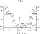
- FIG. 3 is an enlarged cross-sectional view of a structure of the under-cut opening of FIG. 2 where the cathode and auxiliary cathode are connected.
- the organic light-emitting diode display according to the first exemplary embodiment of the present invention comprises a plurality of pixel regions arranged in a matrix on a substrate SUB.
- the organic light-emitting diode display comprises a scan line SL that runs horizontally on the substrate SUB and a data line DL and a drive current line VDD that run vertically on the substrate SUB.
- the pixel regions are defined by the intersections of the scan line SL, data line DL, and drive current line VDD.
- the scan line SL is connected to a gate pad terminal GPT and the data line DL is connected to a data pad terminal DPT.
- the gate terminal GPT has a gate pad GP and a gate pad contact hole GPH and the data pad terminal DPT has a data pad DP and a data pad contact hole DPH.
- the gate pad terminal GPT and data pad terminal DPT are formed of a metal oxide such as ITO or IZO but not limited thereto.
- the thin-film transistors comprise a switching thin-film transistor ST and a driving thin-film transistor DT.
- the switching thin-film transistor ST comprises a switching gate electrode SG, a switching semiconductor layer SA, a switching source electrode SS, and a switching drain electrode SD.
- the switching gate electrode SG is connected to the scan line SL.
- the switching semiconductor layer SA and the central area of the switching gate electrode SG overlap each other, with a gate insulating film GI between them.
- the switching source electrode SS and the switching drain electrode SD are placed on either side of the switching gate electrode SG, and are connected to one side and the other side of the switching semiconductor layer SA, respectively.
- the driving thin-film transistor DT comprises a driving gate electrode DG, a driving semiconductor layer DA, a driving source electrode DS, and a driving drain electrode DD.
- the driving gate electrode DG is connected to the switching drain electrode SD.
- the driving semiconductor layer DA and the central area of the driving gate electrode DG overlap each other, with the gate insulating film GI between them.
- the driving source electrode DS and the driving drain electrode DD are placed on either side of the driving gate electrode DG, and are connected to one side and the other side of the driving semiconductor layer DA, respectively.
- the organic light-emitting diode OLE comprises an anode ANO, an organic emission layer OL, and a cathode CAT.
- the anode ANO is connected to the driving thin-film transistor DT.
- the organic emission layer OL is stacked on the anode ANO.
- a light-emitting area EA is defined in the anode ANO by a bank BN.
- the organic emission layer OL is applied to the entire surface of the substrate SUB, and makes contact with the anode ANO in the light-emitting area EA.
- the cathode CAT also is applied onto the entire surface of the substrate SUB. In the light-emitting area EA, the anode ANO, the organic emission layer OL, and the cathode CAT are sequentially stacked to form the organic light-emitting diode OLE.
- the anode ANO comprises an opaque metal material and the cathode CAT comprises a transparent conductive material.
- the cathode CAT is an electrode that maintains a base voltage in the organic light-emitting diode OLE, and preferably may maintain a constant voltage. If the cathode CAT comprises a transparent conductive material, such as indium tin oxide or indium zinc oxide, which has a much higher resistivity than metals, it is difficult to maintain a constant base voltage in a large-area organic light-emitting diode display.
- it is desirable to reduce surface resistance by forming an auxiliary line AC and/or an auxiliary cathode ACT from metal material and connecting them to the cathode CAT.
- the organic light-emitting diode display further comprises an auxiliary line AC, an auxiliary cathode ACT, and a connecting terminal CT that are placed in a non-light-emitting area surrounding the light-emitting area EA.
- the auxiliary line AC may be made of the same metal material having low-resistivity properties on the same level as a light shielding layer LS that lies under the thin-film transistors ST and DT.
- the auxiliary cathode ACT may be made of the same material on the same level as the source and drain electrodes of the thin-film transistors ST and DT.
- the connecting terminal CT may be made of the same material on the same level as the anode ANO.
- the auxiliary line AC may be formed separately from the light shielding layer LS, or may be connected to the light shielding layer LS to form a mesh pattern on the substrate SUB.
- a buffer layer BUF is applied over the auxiliary line AC.
- the auxiliary cathode ACT may be made of the same material on the same level as the source and drain electrodes of the thin-film transistors ST and DT formed on the buffer layer BUF, but separately from them. In this case, the auxiliary cathode ACT is connected to the auxiliary line AC via an auxiliary line contact hole AH formed through an interlayer insulating film ILD and the buffer layer BUF which are stacked under the source and drain electrodes.
- a passivation film PAS is deposited on the auxiliary cathode ACT.
- a planarization film OC is deposited on the passivation film PAS.
- the anode ANO and the connecting terminal CT are formed on the planarization film OC.
- the auxiliary cathode ACT and the connecting terminal CT may be physically connected to each other, directly or indirectly. Here, it is assumed that they are connected directly.
- the connecting terminal CT is connected to the auxiliary cathode ACT via an under-cut opening OH formed by partially etching the planarization film OC and the passivation film PAS.
- the under-cut opening OH formed through the planarization film OC and the passivation film PAS exposes part of the auxiliary cathode ACT.
- One side of the under-cut opening OH exposes sidewalls of the planarization film OC and passivation film PAS.
- the other side of the under-cut opening OH exposes the end of the connecting terminal CT.
- the connecting terminal CT is exposed through the other side of the under-cut opening OH in order to form an under-area UA by overetching the auxiliary cathode ACT stacked under the connecting terminal CT by using the connecting terminal CT.
- the under-cut opening OH may have a polygonal shape.
- the under-cut opening OH in FIG. 1 has a rectangular shape, but not limited to it.
- the under-cut opening OH may have two opposite sides. On one of the two opposite sides, the etched sidewall of the planarization film OC and the etched sidewall of the passivation film PAS are exposed. On the other side, the connecting terminal CT is exposed, and the under-area UA is formed by overetching the auxiliary cathode ACT lying under the connecting terminal CT.
- the passivation film PAS in the under-cut opening OH is removed. Particularly, on the other side of the under-cut opening OH, part of the auxiliary cathode ACT stacked under the connecting terminal CT is overetched, thereby exposing part of the undersurface of the connecting terminal CT.
- a cave-like space in the under-cut opening OH, formed by overetching the auxiliary cathode ACT under the connecting terminal CT, is defined as the under-area UA.
- the under-area UA is formed by partially removing the auxiliary cathode ACT, with its top being blocked by the connecting terminal CT so as to prevent the organic emission layer OL from being applied to the under-area UA.
- the cathode CAT is deposited all the way into the under-area UA, coming into direct contact with the auxiliary cathode ACT and the connecting terminal CT.
- An enlarged view of the connecting structure of the cathode CAT and the auxiliary cathode ACT using the under-area UA is shown in FIG. 3.
- FIG. 3 is an enlarged cross-sectional view of the under-cut opening indicated by the circle 'A' in FIG. 2 where the cathode and auxiliary cathode are connected.
- the organic emission layer OL is not applied to the under-area UA blocked by the connecting terminal CT because it is an organic material heated and deposited by a thermal deposition technique.
- a metal oxide material such as ITO or IZO, is deposited by a sputtering technique, all the way to the under-area UA blocked by the connecting terminal CT.
- the organic emission layer OL is applied only to the top surface of the connecting terminal CT.
- the cathode CAT is deposited all the way to the underside of the connecting terminal CT blocking the under-area UA, and the connecting terminal CT is physically and electrically connected to the cathode CAT.
- the cathode CAT is connected to the auxiliary cathode ACT and the connecting terminal CT. Also, the auxiliary cathode ACT is connected to the auxiliary line AC.
- the cathode CAT made of a transparent conductive material with high resistivity may have low surface resistance because the auxiliary cathode ACT and the auxiliary line AC are made of a metal material with very low resistivity.
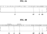
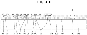
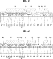
- FIGS. 4A to 4J are cross-sectional views of a manufacturing process of the organic light-emitting diode display according to the first exemplary embodiment of the present invention.
- An opaque metal material is applied onto a substrate SUB.
- the metal material is patterned to form a light shielding layer LS and an auxiliary line AC.
- a buffer layer BUF is formed over the entire surface of the substrate SUB where the light shielding layer LS and the auxiliary line AC are formed.
- the light shielding layer LS is placed where thin-film transistors are to be formed.
- the shielding layer SHL may have the shape of a strip that runs horizontally across the substrate SUB.
- the auxiliary line AC may have the shape of a strip that runs horizontally or vertically across the substrate SUB.
- the auxiliary line AC may be disconnected from the light shielding layer LS or connected to it.
- the auxiliary line AC is illustrated as a line that is connected to the light shielding layer LS and runs vertically across the substrate SUB ( FIG. 4A ).
- a semiconductor material is applied on the buffer layer BUF.
- the semiconductor material is patterned to form a semiconductor layer.
- the semiconductor layer comprises a switching semiconductor layer SA of a switching thin-film transistor ST and a driving semiconductor layer DA of a driving thin-film transistor DT ( FIG. 4B ).
- An insulating material layer and a metal material layer are deposited in a row over the entire surface of the substrate SUB where the semiconductor layers SA and DA are formed.
- the metal material layer and the insulating material layer are patterned simultaneously to form a gate insulating film GI, a scan line SL, a gate pad GP, a first auxiliary capacitor electrode ST1, and gate electrodes.
- the gate electrodes comprise a switching gate electrode SG of the switching thin-film transistor ST and a driving gate electrode DG of the driving thin-film transistor DT.
- the switching gate electrode SG and the center of the switching thin-film transistor SA overlap each other, with the gate insulating film GI between them.
- the driving gate electrode DG and the center of the driving thin-film transistor DA overlap each other, with the gate insulating film GI between the driving gate electrode DG and the driving semiconductor layer DA ( FIG. 4C ).
- An interlayer insulating film ILD is applied over the entire surface of the substrate SUB where the scan line SL, the gate line GP, and the gate electrodes SG and DG are formed.
- the interlayer insulating film ILD is patterned to form contact holes.
- the contact holes expose two opposite sides of the switching thin-film transistor ST and driving thin-film transistor DT.
- the two opposite sides are either side of the gate electrodes SG and DG of the semiconductor layers SA and DA. Also, they expose part of the driving gate electrode DG.
- an auxiliary line contact hole AH is formed through the interlayer insulating film ILD and the buffer layer BUF to expose part of the auxiliary line AC ( FIG. 4D ).
- a metal material is applied on the interlayer insulating film ILD in which contact holes including the auxiliary line contact hole AH are formed.
- the metal material is patterned to form a data line DL, a drive current line VDD, an auxiliary cathode ACT, a second auxiliary capacitor electrode ST2, and source and drain electrodes.
- the source and drain electrodes comprise a scan source electrode SS, a scan drain electrode SD, a driving source electrode DS, and a driving drain electrode DD.
- the scan source electrode SS is branched from the data line DL.
- the driving source electrode DS is branched from the driving current line VDD.
- a data pad DP is placed at the end of the data line DL, and a driving pad VDP is placed at the end of the drive current line VDD. Also, a gate pad connecting terminal GP1 is formed at the gate pad GP.
- the second auxiliary capacitor electrode ST2 extends from the driving drain electrode DD, and overlaps the first auxiliary capacitor electrode ST1, with the interlayer insulating film ILD between them ( FIG. 4E ).
- a passivation film PAS is applied over the entire surface of the substrate SUB where the source and drain electrodes are formed. Subsequently, a planarization film OC is applied on the passivation film PAS. In a sixth mask process, the planarization film OC is patterned to form a first pixel contact hole PH1 and a first under-cut opening OH1. In this instance, it is desirable that the planarization film OC in the area above the gate pad GP and data pad DP also is removed.
- the first under-cut opening OH1 which is a part for exposing the auxiliary cathode ACT, is preferably formed in the non-light-emitting area where the organic light-emitting diode is not placed ( FIG. 4F ).
- the exposed passivation film PAS is patterned to form a gate pad contact hole GPH, a data pad contact hole DPH, a pixel contact hole PH, and a second under-cut opening OH2.
- the gate pad contact hole GPH exposes the gate pad connecting terminal GP1.
- the data pad contact hole DPH exposes the data pad terminal DP.
- the pixel contact hole PH exposes one end of the driving drain electrode DD.
- the second under-cut opening OH2 may be the same size as the first under-cut opening OH1 For convenience, the description will be given on the assumption that the second under-cut opening OH2 is a size small enough to fit into the first under-cut opening OH1 ( FIG. 4G ).
- a metal material is deposited over the entire surface of the substrate SUB where the planarization film OC comprising the contact holes GPH, DPH, and PH and the second under-cut opening OH2 is formed.
- the metal material is three layers of metal formed by sequentially stacking indium tin oxide, molybdenum titanium alloy, and indium tin oxide.
- the molybdenum titanium stacked in the middle may be replaced with silver (Ag) or aluminum (Al).
- the metal material is patterned to form an anode ANO and a connecting terminal CT.
- the anode ANO is shaped to take up most of the center of the pixel region..
- the eighth mask process it is preferable to overetch the auxiliary cathode ACT making contact with the underside of the connecting terminal CT by adjusting the etching time in an etching process in which the anode ANO and the connecting terminal CT are formed.
- the end of the auxiliary cathode ACT making contact with the undersurface of the connecting terminal CT is partially etched away to form an under-area UA under the connecting terminal CT.
- an under-cut opening OH comprising the under-area UA is formed.
- On one side of the under-cut opening OH is a sidewall formed by etching the planarization film OC and the passivation film PAS.
- the end of the auxiliary cathode ACT and the end of the overlying connecting terminal CT making contact with the auxiliary cathode ACT are exposed.
- the end of the auxiliary cathode ACT is recessed to a certain depth further inward than the end of the connecting terminal CT ( FIG. 4H ).
- An organic material is applied over the entire surface of the substrate SUB where the anode ANO and the connecting terminal CT are formed.
- the organic material is patterned to form a bank BN.
- the bank BN exposes most of the anode ANO and defines the light-emitting area EA. Also, the bank BN exposes the entire under-cut opening OH. That is, the bank BN has an open area smaller than the anode ANO and an open area larger than the under-cut opening OH ( FIG. 4I ).
- An organic emission layer OL is applied over the entire surface of the substrate SUB where the bank BN is formed.
- the organic emission layer OL is an organic material that is applied by a thermal deposition process.
- the organic emission layer OL is applied to cover the surface of the bank BN and the top of the anode ANO.
- the organic emission layer OL is applied over only some part of the exposed surface of the auxiliary cathode ACT. Particularly, in the under-area UA, the organic emission layer OL is not applied, but the side of the auxiliary cathode ACT is exposed directly.
- a transparent conductive material is then applied to form the cathode CAT.
- the transparent conductive material comprises indium tin oxide (ITO) or indium zinc oxide (IZO).
- the transparent conductive material is formed by a sputtering technique.
- the cathode CAT is stacked on top of the anode ANO and the organic emission layer OL, thereby forming the organic light-emitting diode OLE.
- the cathode CAT deposited by the sputtering technique tends to be deposited along the bends on the surface. Also, the metal materials formed by the sputtering technique tend to accumulate one upon another as if the deposited particles grow. Thus, the cathode CAT is deposited in the area where the organic emission layer OL is not applied, as well as on the surface of the organic emission layer OL. That is, in the under-cut opening OH, the cathode CAT is deposited along the sloping surface on one side where the connecting terminal CT is not formed, and extends all the way to the under-area UA.
- the cathode CAT penetrates into the under-area UA where the organic emission layer OL is not applied, and comes into direct contact with the side of the auxiliary cathode ACT. Moreover, the cathode CAT comes into direct contact with the exposed side of the connecting terminal CT in the under-cut opening OH, which is not covered by the organic emission layer OL. Particularly, the connecting terminal CT protrudes from the top of the auxiliary cathode ACT, and the cathode CAT extends as if to wrap the exposed part not covered by the organic emission layer OL ( FIG. 4J ).
- the auxiliary cathode ACT In the under-cut opening OH, the auxiliary cathode ACT, the connecting terminal CT, and the cathode CAT are sequentially brought into contact with one another.
- the auxiliary cathode ACT is connected to the auxiliary line AC via the auxiliary contact hole AH.
- the cathode CAT is connected to the auxiliary line AC made of low-resistivity material, thereby maintaining low surface resistance.
- FIG. 5 The basic configuration of an organic light-emitting diode display according to the second exemplary embodiment is identical to that of the first exemplary embodiment.
- the only difference is the structure of part of the under-cut opening OH.
- the description below focuses on the structure of the under-cut portion.
- the manufacturing process also is identical to that of the first exemplary embodiment, except for the difference in the type of material used.
- a description of the process, if required, will be given referring to the drawings of the first exemplary embodiment.
- FIG. 5 is an enlarged cross-sectional view of a structure of an under-cut opening where a cathode and an auxiliary cathode are connected, in an organic light-emitting diode display according to a second exemplary embodiment of the present invention taken along the line I-I' in FIG. 1 .
- the second exemplary embodiment proposes a structure that is generally applied to a large-area, top-emissive organic light-emitting diode display according to the present invention.
- the data line DL is longer. Therefore, it is necessary that the data line DL be made of a low-resistivity material.
- the data line DL and the source and drain electrodes and auxiliary cathode ACT made of the same material on the same level as the data line DL may be made of a low-resistivity material such as copper (Cu).
- Copper corrodes readily on its surface when exposed to heat in the manufacturing process. Copper, if it is formed on an insulating material or covers the insulating material, may have unstable interfacial characteristics or have an impurity such as a hillock or may be peeled off or come off. To prevent this problem, it is preferable to use a three-layer structure in which underlying and overlying passivation metal layers are stacked, rather than using a single layer of copper Cu.
- the data line DL, source and drain electrodes, and auxiliary cathode ACT may have a three-layer structure in which a lower passivation metal layer MT1 comprising molybdenum-titanium (Mo-Ti) alloy, a low-resistivity metal layer CU comprising copper, and an upper passivation metal layer MT2 comprising molybdenum-titanium (Mo-Ti) alloy are sequentially stacked.
- a lower passivation metal layer MT1 comprising molybdenum-titanium (Mo-Ti) alloy
- a low-resistivity metal layer CU comprising copper
- an upper passivation metal layer MT2 comprising molybdenum-titanium (Mo-Ti) alloy
- the sidewall of the stack of the lower passivation metal layer MT1, low-resistivity metal layer CU, and upper passivation metal layer MT2 is exposed directly.
- the anode ANO and the connecting terminal CT are formed, and oxidation may occur on the low-resistivity metal layer CU comprising copper exposed in a thermal treatment process for device stabilization. Unless this oxidation is prevented, corrosion may progress over time, causing defects throughout the auxiliary cathode ACT.
- the bank BN is left in the under-area UA upon formation of the bank BN shown in FIG. 4I , so that a dummy bank BND is provided to protect the etched side of the auxiliary cathode ACT.
- a dummy bank BND filling part of the under-area UA, corrosion on the etched side of the auxiliary cathode ACT may be avoided.
- the cathode CAT and the auxiliary cathode ACT do not come into direct contact with each other due to the dummy bank BND.
- the cathode CAT may extend along the side of the dummy bank BND filling part of the under-area UA and come into direct contact with the underside of the overlying connecting terminal CT. That is, as shown in FIG. 5 , the cathode CAT may extend from one side of the under-cut opening OH according to the second exemplary embodiment, along the sidewall of the dummy bank BND filling part of the under-area UA, and come into contact with the undersurface of the overlying connecting terminal CT. Moreover, on the other side, the cathode CAT extends as if to wrap the side and bottom of the exposed end of the connecting terminal CT which are not covered by the organic emission layer OL.
- the dummy bank BND filling part of the under-area UA may be formed by adjusting the amount of exposure in a photolithography process for forming the bank BN described with respect to FIG. 4I .
- the bank BN may be left in some of the space in the under-area UA by adjusting exposure time or exposure energy.
- the bank BN may be left in the under-area UA by reducing the amount of exposure using a half-tone mask, thereby forming the dummy bank BND.
Landscapes
- Engineering & Computer Science (AREA)
- Microelectronics & Electronic Packaging (AREA)
- Physics & Mathematics (AREA)
- Optics & Photonics (AREA)
- Geometry (AREA)
- Manufacturing & Machinery (AREA)
- Electroluminescent Light Sources (AREA)
Abstract
Description
- This application claims the benefit of Korea Patent Application No.
10-2017-0182076 filed on December 28, 2017 - The present invention relates to a top-emissive organic light-emitting diode display. More particularly, the present invention relates to a top-emissive organic light-emitting diode display that comprises an auxiliary cathode for reducing the surface resistance of a cathode and has an under-cut structure configured to directly connect the auxiliary electrode and the cathode.
- Recently, various flat-panel displays that are less bulky and more lightweight than cathode ray tubes (CRTs) are being developed. Examples of these flat panel displays include liquid crystal displays (LCDs), field emission displays (FEDs), plasma display panels (PDPs), electroluminescence devices (ELs), etc.
- Electroluminescence displays are roughly classified into inorganic electroluminescence displays and organic light-emitting diode displays depending on the materials used for an emissive layer, and offer several advantages such as fast response time, high light-emission efficiency, high brightness, and wide viewing angle because of their self-emissive elements. Notably, there is a rapidly increasing demand for organic light-emitting diode displays, which have high energy efficiency and less leakage current and facilitate grayscale representation through current control.
- In an organic light-emitting diode display, a cathode with a base voltage is applied across the entire surface of a display panel. Although there is no problem when the cathode is made of a metal material with low resistivity, there may be problems with image quality if the cathode is made of a transparent conductive material, due to its high surface resistance.
- For example, the surface resistance increases if the cathode comprises a transparent conductive material or a material that has a higher resistivity than metals, such as indium tin oxide or indium zinc oxide, as in top-emissive displays. As a result, the voltage of the cathode may not be constant across the entire area of the display panel. The uneven brightness of the display device across the entire screen may become a more important issue, especially in the development of large-area organic light-emitting diode displays.
- The present invention has been made in an effort to overcome the aforementioned problems, and an aspect of the present invention is to provide a large-area organic light-emitting diode display that has good display quality because the surface resistance is low due to direct contact between a cathode and an auxiliary cathode. Another aspect of the present invention is to provide a large-area organic light-emitting diode display that comprises an auxiliary cathode and simplifies the manufacturing process. Various embodiments provide an organic light-emitting diode display according to
claim 1. Further embodiments are described in the dependent claims. - Various embodiments of the present invention provide an organic light-emitting diode display comprising a substrate, an auxiliary cathode, a passivation film, a planarization film, an under-cut opening, a connecting terminal, an under-area, a bank, an organic emission layer, and a cathode. The auxiliary cathode is placed on the substrate. The passivation film covers the auxiliary cathode. The planarization film is stacked on the passivation film. The under-cut opening is formed in the passivation film and the planarization film and exposes one end of the auxiliary cathode. The connecting terminal makes contact with the top surface of the one end exposed through the under-cut opening and protrudes into the under-cut opening, being longer in length than the one end of the auxiliary cathode. The under-area is formed between the end of the connecting terminal and the one end of the auxiliary cathode. The bank lies on the planarization film and exposes the entire under-cut opening in a larger size than the under-cut opening. The organic emission layer covers the surface of the connecting terminal in the under-cut opening, and is not applied to the under-area and exposes the side of the connecting terminal. The cathode is stacked on the organic emission layer, makes contact with the side of the connecting terminal not covered by the organic emission layer, and extends all the way to the under-area.
- In at least one embodiment, the under-cut opening comprises: one side where the sidewalls of the planarization film and passivation film are etched; and another side (e.g, opposite side) that exposes the end of the connecting terminal and the one end of the auxiliary cathode, where the under-area is formed under the exposed end of the connecting terminal.
- In at least one embodiment, the organic light-emitting diode display further comprises: a interlayer insulating film on the substrate that lies under the auxiliary cathode; a buffer layer stacked under the interlayer insulating film; and an auxiliary line stacked under the buffer layer and connected to the auxiliary cathode.
- In at least one embodiment, the organic light-emitting diode display further comprises: a light shielding layer on the substrate that lies on the same level as the auxiliary line; a thin-film transistor on the light shielding layer that lies under the interlayer insulating film; a pixel contact hole formed in the planarization film that exposes part of the thin-film transistor; an anode on the planarization film that is connected to the thin-film transistor via the pixel contact hole, wherein the bank further comprises a light-emitting area that exposes the center of the anode, the organic emission layer is applied over the entire light-emitting area, the cathode is stacked on the organic emission layer in the light-emitting area, and the anode, the organic emission layer, and the cathode overlap to form an organic light-emitting diode in the light-emitting area.
- In at least one embodiment, the connecting terminal has a three-layer structure comprising a metal material layer and transparent conductive layers stacked over and under the metal material layer.
- In at least one embodiment, the buffer layer covers the light shielding layer and the auxiliary line; and the organic light-emitting diode display further comprises source and drain electrodes of the thin-film transistor that lie over the interlayer insulating film, wherein the auxiliary cathode comprises the same material as the source and drain electrodes.
- In at least one embodiment, in the under-cut opening, the one end of the auxiliary cathode, the end of the connecting terminal, and the cathode are physically and electrically connected by coming into direct contact with one another.
- In at least one embodiment, the organic light-emitting diode display further comprises a dummy bank that comes into direct contact with the end of the auxiliary cathode in the under-area.
- In at least one embodiment, the dummy bank comprises the same material as the bank.
- In at least one embodiment, the auxiliary cathode comprises: a first passivation metal layer; a low-resistivity metal layer stacked on the first passivation metal layer; and a second passivation metal layer stacked on the low-resistivity metal layer.
- In at least one embodiment, the dummy bank fills part of the under-area.
- In at least one embodiment, the cathode on one side of the under-cut opening extends to the dummy bank, and the cathode on the other side is physically and electrically connected to the connecting terminal by coming into contact with the connecting terminal, while wrapping the exposed end of the connecting terminal not covered by the organic emission layer, wherein the cathode and the auxiliary cathode are electrically connected via the connecting terminal.
- The organic light-emitting diode display according to various embodiments of the present invention is provided as a large-area organic light-emitting diode display in which an auxiliary cathode is formed by using a shielding layer for protecting a metal oxide semiconductor material from light coming from the outside. The auxiliary cathode and the cathode may be physically and electrically connected, without an additional mask process, by forming an under-cut structure in a passivation film patterning process. Various embodiments of the present invention provide a large-area organic light-emitting diode display because of its structure capable of reducing the resistance of the cathode. Moreover, the manufacturing time and costs can be reduced by reducing the number of mask processes.
- The accompanying drawings, which are included to provide a further understanding of the invention and are incorporated in and constitute a part of this specification, illustrate embodiments of the invention and together with the description serve to explain the principles of the invention.
- In the drawings:
-
FIG. 1 is a plan view of a structure of an organic light-emitting diode display according to the present invention; -
FIG. 2 is a cross-sectional view of the organic light-emitting diode display according to the first exemplary embodiment of the present invention, taken along the line I-I' inFIG. 1 ; -
FIG. 3 is an enlarged cross-sectional view of a structure of the under-cut opening ofFIG. 2 where the cathode and auxiliary cathode are connected; -
FIGS. 4A to 4J are cross-sectional views of some of the steps of a manufacturing process of the organic light-emitting diode display according to the first exemplary embodiment of the present invention; and -
FIG. 5 is an enlarged cross-sectional view of a structure of an under-cut opening where a cathode and an auxiliary cathode are connected, in an organic light-emitting diode display according to a second exemplary embodiment of the present invention taken along the line I-I' inFIG. 1 . - Various aspects and features of the present invention and methods of accomplishing them may be understood more readily by reference to the following detailed descriptions of exemplary embodiments and the accompanying drawings. The present invention may, however, be embodied in many different forms and should not be construed as being limited to the exemplary embodiments set forth herein. Rather, these exemplary embodiments are provided so that this disclosure will be thorough and complete and will fully convey the concept of the present invention to those skilled in the art, and the present invention is defined by the appended claims.
- The shapes, sizes, proportions, angles, numbers, etc. shown in the figures to describe the exemplary embodiments of the present invention are merely examples and not limited to those shown in the figures. Like reference numerals denote like elements throughout the specification.
- In describing the present invention, detailed descriptions of related well-known technologies will be omitted to avoid unnecessary obscuring the present invention. When the terms 'comprise', 'have', 'consist of' and the like are used, other parts may be added as long as the term 'only' is not used. The singular forms may be interpreted as the plural forms unless explicitly stated.
- The elements may be interpreted to include an error margin even if not explicitly stated. When the position relation between two parts is described using the terms "on", "over", "under", "next to" and the like, one or more parts may be positioned between the two parts as long as the term "immediately" or "directly" is not used.
- It will be understood that, although the terms "first", "second", etc. may be used herein to describe various elements, these elements are not limited by these terms. These terms are used to distinguish one element from another element. The terms and names of elements used herein are chosen for ease of description and may be different from the names of parts used in actual products.
- The features of various exemplary embodiments of the present invention may be coupled or combined with one another either partly or wholly, and may technically interact or work together in various ways. The exemplary embodiments may be carried out independently or in connection with one another.
- Hereinafter, exemplary embodiments of the present invention will be described in detail with reference to the accompanying drawings. In the exemplary embodiments below, the description of an electroluminescence display will focus on an organic light-emitting display comprising organic light-emitting material. However, it should be noted that the technical idea of the present invention is not limited to organic light-emitting displays but also may apply to inorganic light-emitting displays comprising inorganic light-emitting material.
- Hereinafter, a structure of an organic light-emitting diode display according to a first exemplary embodiment of the present invention will be described with reference to
FIGS. 1 to 3 .FIG. 1 is a plan view of a structure of an organic light-emitting diode display according to the present invention.FIG. 2 is a cross-sectional view of the organic light-emitting diode display according to the first exemplary embodiment of the present invention, taken along the line I-I' inFIG. 1 .FIG. 3 is an enlarged cross-sectional view of a structure of the under-cut opening ofFIG. 2 where the cathode and auxiliary cathode are connected. - The organic light-emitting diode display according to the first exemplary embodiment of the present invention comprises a plurality of pixel regions arranged in a matrix on a substrate SUB. The organic light-emitting diode display comprises a scan line SL that runs horizontally on the substrate SUB and a data line DL and a drive current line VDD that run vertically on the substrate SUB. The pixel regions are defined by the intersections of the scan line SL, data line DL, and drive current line VDD. The scan line SL is connected to a gate pad terminal GPT and the data line DL is connected to a data pad terminal DPT. The gate terminal GPT has a gate pad GP and a gate pad contact hole GPH and the data pad terminal DPT has a data pad DP and a data pad contact hole DPH. For example, the gate pad terminal GPT and data pad terminal DPT are formed of a metal oxide such as ITO or IZO but not limited thereto.
- In each pixel region, an organic light-emitting diode OLE and thin-film transistors, which are driving elements for driving the organic light-emitting diode OLE, are placed. The thin-film transistors comprise a switching thin-film transistor ST and a driving thin-film transistor DT. The switching thin-film transistor ST comprises a switching gate electrode SG, a switching semiconductor layer SA, a switching source electrode SS, and a switching drain electrode SD. The switching gate electrode SG is connected to the scan line SL. The switching semiconductor layer SA and the central area of the switching gate electrode SG overlap each other, with a gate insulating film GI between them. The switching source electrode SS and the switching drain electrode SD are placed on either side of the switching gate electrode SG, and are connected to one side and the other side of the switching semiconductor layer SA, respectively.
- The driving thin-film transistor DT comprises a driving gate electrode DG, a driving semiconductor layer DA, a driving source electrode DS, and a driving drain electrode DD. The driving gate electrode DG is connected to the switching drain electrode SD. The driving semiconductor layer DA and the central area of the driving gate electrode DG overlap each other, with the gate insulating film GI between them. The driving source electrode DS and the driving drain electrode DD are placed on either side of the driving gate electrode DG, and are connected to one side and the other side of the driving semiconductor layer DA, respectively.
- The organic light-emitting diode OLE comprises an anode ANO, an organic emission layer OL, and a cathode CAT. The anode ANO is connected to the driving thin-film transistor DT. The organic emission layer OL is stacked on the anode ANO. Particularly, a light-emitting area EA is defined in the anode ANO by a bank BN. The organic emission layer OL is applied to the entire surface of the substrate SUB, and makes contact with the anode ANO in the light-emitting area EA. The cathode CAT also is applied onto the entire surface of the substrate SUB. In the light-emitting area EA, the anode ANO, the organic emission layer OL, and the cathode CAT are sequentially stacked to form the organic light-emitting diode OLE.
- In the case of a top-emissive organic light-emitting diode display, light is directed from the anode ANO toward the cathode CAT in
FIG. 2 . Thus, it is desirable that the anode ANO comprises an opaque metal material and the cathode CAT comprises a transparent conductive material. The cathode CAT is an electrode that maintains a base voltage in the organic light-emitting diode OLE, and preferably may maintain a constant voltage. If the cathode CAT comprises a transparent conductive material, such as indium tin oxide or indium zinc oxide, which has a much higher resistivity than metals, it is difficult to maintain a constant base voltage in a large-area organic light-emitting diode display. Thus, it is desirable to reduce surface resistance by forming an auxiliary line AC and/or an auxiliary cathode ACT from metal material and connecting them to the cathode CAT. - To this end, in the first exemplary embodiment of the present invention, the organic light-emitting diode display further comprises an auxiliary line AC, an auxiliary cathode ACT, and a connecting terminal CT that are placed in a non-light-emitting area surrounding the light-emitting area EA. The auxiliary line AC may be made of the same metal material having low-resistivity properties on the same level as a light shielding layer LS that lies under the thin-film transistors ST and DT. The auxiliary cathode ACT may be made of the same material on the same level as the source and drain electrodes of the thin-film transistors ST and DT. The connecting terminal CT may be made of the same material on the same level as the anode ANO.
- The auxiliary line AC may be formed separately from the light shielding layer LS, or may be connected to the light shielding layer LS to form a mesh pattern on the substrate SUB. A buffer layer BUF is applied over the auxiliary line AC. The auxiliary cathode ACT may be made of the same material on the same level as the source and drain electrodes of the thin-film transistors ST and DT formed on the buffer layer BUF, but separately from them. In this case, the auxiliary cathode ACT is connected to the auxiliary line AC via an auxiliary line contact hole AH formed through an interlayer insulating film ILD and the buffer layer BUF which are stacked under the source and drain electrodes.
- A passivation film PAS is deposited on the auxiliary cathode ACT. A planarization film OC is deposited on the passivation film PAS. The anode ANO and the connecting terminal CT are formed on the planarization film OC. The auxiliary cathode ACT and the connecting terminal CT may be physically connected to each other, directly or indirectly. Here, it is assumed that they are connected directly. The connecting terminal CT is connected to the auxiliary cathode ACT via an under-cut opening OH formed by partially etching the planarization film OC and the passivation film PAS.
- Moreover, the under-cut opening OH formed through the planarization film OC and the passivation film PAS exposes part of the auxiliary cathode ACT. One side of the under-cut opening OH exposes sidewalls of the planarization film OC and passivation film PAS. The other side of the under-cut opening OH exposes the end of the connecting terminal CT. The connecting terminal CT is exposed through the other side of the under-cut opening OH in order to form an under-area UA by overetching the auxiliary cathode ACT stacked under the connecting terminal CT by using the connecting terminal CT.
- The under-cut opening OH may have a polygonal shape. For convenience of explanation, the under-cut opening OH in
FIG. 1 has a rectangular shape, but not limited to it. For example, the under-cut opening OH may have two opposite sides. On one of the two opposite sides, the etched sidewall of the planarization film OC and the etched sidewall of the passivation film PAS are exposed. On the other side, the connecting terminal CT is exposed, and the under-area UA is formed by overetching the auxiliary cathode ACT lying under the connecting terminal CT. - The passivation film PAS in the under-cut opening OH is removed. Particularly, on the other side of the under-cut opening OH, part of the auxiliary cathode ACT stacked under the connecting terminal CT is overetched, thereby exposing part of the undersurface of the connecting terminal CT. A cave-like space in the under-cut opening OH, formed by overetching the auxiliary cathode ACT under the connecting terminal CT, is defined as the under-area UA.
- The under-area UA is formed by partially removing the auxiliary cathode ACT, with its top being blocked by the connecting terminal CT so as to prevent the organic emission layer OL from being applied to the under-area UA. On the other hand, the cathode CAT is deposited all the way into the under-area UA, coming into direct contact with the auxiliary cathode ACT and the connecting terminal CT. An enlarged view of the connecting structure of the cathode CAT and the auxiliary cathode ACT using the under-area UA is shown in
FIG. 3. FIG. 3 is an enlarged cross-sectional view of the under-cut opening indicated by the circle 'A' inFIG. 2 where the cathode and auxiliary cathode are connected. - The organic emission layer OL is not applied to the under-area UA blocked by the connecting terminal CT because it is an organic material heated and deposited by a thermal deposition technique. On the other hand, a metal oxide material such as ITO or IZO, is deposited by a sputtering technique, all the way to the under-area UA blocked by the connecting terminal CT.
- Moreover, the organic emission layer OL is applied only to the top surface of the connecting terminal CT. On the other hand, the cathode CAT is deposited all the way to the underside of the connecting terminal CT blocking the under-area UA, and the connecting terminal CT is physically and electrically connected to the cathode CAT.
- That is, in the under-cut opening of the organic light-emitting diode display according to the first exemplary embodiment of the present invention, the cathode CAT is connected to the auxiliary cathode ACT and the connecting terminal CT. Also, the auxiliary cathode ACT is connected to the auxiliary line AC. Thus, the cathode CAT made of a transparent conductive material with high resistivity may have low surface resistance because the auxiliary cathode ACT and the auxiliary line AC are made of a metal material with very low resistivity.
- Hereinafter, a manufacturing process of the organic light-emitting diode display according to the first exemplary embodiment of the present invention will be described with reference to
FIGS. 4A to 4J. FIGS. 4A to 4J are cross-sectional views of a manufacturing process of the organic light-emitting diode display according to the first exemplary embodiment of the present invention. - An opaque metal material is applied onto a substrate SUB. In a first mask process, the metal material is patterned to form a light shielding layer LS and an auxiliary line AC. A buffer layer BUF is formed over the entire surface of the substrate SUB where the light shielding layer LS and the auxiliary line AC are formed. The light shielding layer LS is placed where thin-film transistors are to be formed. For example, the shielding layer SHL may have the shape of a strip that runs horizontally across the substrate SUB. The auxiliary line AC may have the shape of a strip that runs horizontally or vertically across the substrate SUB. The auxiliary line AC may be disconnected from the light shielding layer LS or connected to it. Here, as shown in
FIG. 2 , the auxiliary line AC is illustrated as a line that is connected to the light shielding layer LS and runs vertically across the substrate SUB (FIG. 4A ). - A semiconductor material is applied on the buffer layer BUF. In a second mask process, the semiconductor material is patterned to form a semiconductor layer. The semiconductor layer comprises a switching semiconductor layer SA of a switching thin-film transistor ST and a driving semiconductor layer DA of a driving thin-film transistor DT (
FIG. 4B ). - An insulating material layer and a metal material layer are deposited in a row over the entire surface of the substrate SUB where the semiconductor layers SA and DA are formed. In a third mask process, the metal material layer and the insulating material layer are patterned simultaneously to form a gate insulating film GI, a scan line SL, a gate pad GP, a first auxiliary capacitor electrode ST1, and gate electrodes. The gate electrodes comprise a switching gate electrode SG of the switching thin-film transistor ST and a driving gate electrode DG of the driving thin-film transistor DT. The switching gate electrode SG and the center of the switching thin-film transistor SA overlap each other, with the gate insulating film GI between them. The driving gate electrode DG and the center of the driving thin-film transistor DA overlap each other, with the gate insulating film GI between the driving gate electrode DG and the driving semiconductor layer DA (
FIG. 4C ). - An interlayer insulating film ILD is applied over the entire surface of the substrate SUB where the scan line SL, the gate line GP, and the gate electrodes SG and DG are formed. In a fourth mask process, the interlayer insulating film ILD is patterned to form contact holes. The contact holes expose two opposite sides of the switching thin-film transistor ST and driving thin-film transistor DT. The two opposite sides are either side of the gate electrodes SG and DG of the semiconductor layers SA and DA. Also, they expose part of the driving gate electrode DG. Moreover, an auxiliary line contact hole AH is formed through the interlayer insulating film ILD and the buffer layer BUF to expose part of the auxiliary line AC (
FIG. 4D ). - A metal material is applied on the interlayer insulating film ILD in which contact holes including the auxiliary line contact hole AH are formed. In a fifth mask process, the metal material is patterned to form a data line DL, a drive current line VDD, an auxiliary cathode ACT, a second auxiliary capacitor electrode ST2, and source and drain electrodes. The source and drain electrodes comprise a scan source electrode SS, a scan drain electrode SD, a driving source electrode DS, and a driving drain electrode DD. The scan source electrode SS is branched from the data line DL. The driving source electrode DS is branched from the driving current line VDD. A data pad DP is placed at the end of the data line DL, and a driving pad VDP is placed at the end of the drive current line VDD. Also, a gate pad connecting terminal GP1 is formed at the gate pad GP. The second auxiliary capacitor electrode ST2 extends from the driving drain electrode DD, and overlaps the first auxiliary capacitor electrode ST1, with the interlayer insulating film ILD between them (
FIG. 4E ). - A passivation film PAS is applied over the entire surface of the substrate SUB where the source and drain electrodes are formed. Subsequently, a planarization film OC is applied on the passivation film PAS. In a sixth mask process, the planarization film OC is patterned to form a first pixel contact hole PH1 and a first under-cut opening OH1. In this instance, it is desirable that the planarization film OC in the area above the gate pad GP and data pad DP also is removed. The first under-cut opening OH1, which is a part for exposing the auxiliary cathode ACT, is preferably formed in the non-light-emitting area where the organic light-emitting diode is not placed (
FIG. 4F ). - In a seventh mask process, the exposed passivation film PAS is patterned to form a gate pad contact hole GPH, a data pad contact hole DPH, a pixel contact hole PH, and a second under-cut opening OH2. The gate pad contact hole GPH exposes the gate pad connecting terminal GP1. The data pad contact hole DPH exposes the data pad terminal DP. The pixel contact hole PH exposes one end of the driving drain electrode DD. The second under-cut opening OH2 may be the same size as the first under-cut opening OH1 For convenience, the description will be given on the assumption that the second under-cut opening OH2 is a size small enough to fit into the first under-cut opening OH1 (
FIG. 4G ). - A metal material is deposited over the entire surface of the substrate SUB where the planarization film OC comprising the contact holes GPH, DPH, and PH and the second under-cut opening OH2 is formed. Preferably, the metal material is three layers of metal formed by sequentially stacking indium tin oxide, molybdenum titanium alloy, and indium tin oxide. Here, the molybdenum titanium stacked in the middle may be replaced with silver (Ag) or aluminum (Al). In an eighth mask process, the metal material is patterned to form an anode ANO and a connecting terminal CT. The anode ANO is shaped to take up most of the center of the pixel region..
- In the eighth mask process, it is preferable to overetch the auxiliary cathode ACT making contact with the underside of the connecting terminal CT by adjusting the etching time in an etching process in which the anode ANO and the connecting terminal CT are formed. As a result, the end of the auxiliary cathode ACT making contact with the undersurface of the connecting terminal CT is partially etched away to form an under-area UA under the connecting terminal CT. As such, an under-cut opening OH comprising the under-area UA is formed. On one side of the under-cut opening OH is a sidewall formed by etching the planarization film OC and the passivation film PAS. On the other side, the end of the auxiliary cathode ACT and the end of the overlying connecting terminal CT making contact with the auxiliary cathode ACT are exposed. Particularly, the end of the auxiliary cathode ACT is recessed to a certain depth further inward than the end of the connecting terminal CT (
FIG. 4H ). - An organic material is applied over the entire surface of the substrate SUB where the anode ANO and the connecting terminal CT are formed. In a ninth mask process, the organic material is patterned to form a bank BN. The bank BN exposes most of the anode ANO and defines the light-emitting area EA. Also, the bank BN exposes the entire under-cut opening OH. That is, the bank BN has an open area smaller than the anode ANO and an open area larger than the under-cut opening OH (
FIG. 4I ). - An organic emission layer OL is applied over the entire surface of the substrate SUB where the bank BN is formed. The organic emission layer OL is an organic material that is applied by a thermal deposition process. The organic emission layer OL is applied to cover the surface of the bank BN and the top of the anode ANO. In the under-cut opening OH, the organic emission layer OL is applied over only some part of the exposed surface of the auxiliary cathode ACT. Particularly, in the under-area UA, the organic emission layer OL is not applied, but the side of the auxiliary cathode ACT is exposed directly.
- After applying the organic emission layer OL, a transparent conductive material is then applied to form the cathode CAT. The transparent conductive material comprises indium tin oxide (ITO) or indium zinc oxide (IZO). The transparent conductive material is formed by a sputtering technique. In the light-emitting area EA, the cathode CAT is stacked on top of the anode ANO and the organic emission layer OL, thereby forming the organic light-emitting diode OLE.
- The cathode CAT deposited by the sputtering technique tends to be deposited along the bends on the surface. Also, the metal materials formed by the sputtering technique tend to accumulate one upon another as if the deposited particles grow. Thus, the cathode CAT is deposited in the area where the organic emission layer OL is not applied, as well as on the surface of the organic emission layer OL. That is, in the under-cut opening OH, the cathode CAT is deposited along the sloping surface on one side where the connecting terminal CT is not formed, and extends all the way to the under-area UA. As a result, the cathode CAT penetrates into the under-area UA where the organic emission layer OL is not applied, and comes into direct contact with the side of the auxiliary cathode ACT. Moreover, the cathode CAT comes into direct contact with the exposed side of the connecting terminal CT in the under-cut opening OH, which is not covered by the organic emission layer OL. Particularly, the connecting terminal CT protrudes from the top of the auxiliary cathode ACT, and the cathode CAT extends as if to wrap the exposed part not covered by the organic emission layer OL (
FIG. 4J ). - In the under-cut opening OH, the auxiliary cathode ACT, the connecting terminal CT, and the cathode CAT are sequentially brought into contact with one another. The auxiliary cathode ACT is connected to the auxiliary line AC via the auxiliary contact hole AH. As a result, the cathode CAT is connected to the auxiliary line AC made of low-resistivity material, thereby maintaining low surface resistance.
- Hereinafter, a second exemplary embodiment of the present invention will be described with reference to
FIG. 5 . The basic configuration of an organic light-emitting diode display according to the second exemplary embodiment is identical to that of the first exemplary embodiment. The only difference is the structure of part of the under-cut opening OH. Thus, the description below focuses on the structure of the under-cut portion. The description will be given referring again toFIG. 1 because no difference is found on the plane. The manufacturing process also is identical to that of the first exemplary embodiment, except for the difference in the type of material used. Thus, a description of the process, if required, will be given referring to the drawings of the first exemplary embodiment.FIG. 5 is an enlarged cross-sectional view of a structure of an under-cut opening where a cathode and an auxiliary cathode are connected, in an organic light-emitting diode display according to a second exemplary embodiment of the present invention taken along the line I-I' inFIG. 1 . - The second exemplary embodiment proposes a structure that is generally applied to a large-area, top-emissive organic light-emitting diode display according to the present invention. In the large-area display, the data line DL is longer. Therefore, it is necessary that the data line DL be made of a low-resistivity material. For example, the data line DL and the source and drain electrodes and auxiliary cathode ACT made of the same material on the same level as the data line DL may be made of a low-resistivity material such as copper (Cu).
- Copper corrodes readily on its surface when exposed to heat in the manufacturing process. Copper, if it is formed on an insulating material or covers the insulating material, may have unstable interfacial characteristics or have an impurity such as a hillock or may be peeled off or come off. To prevent this problem, it is preferable to use a three-layer structure in which underlying and overlying passivation metal layers are stacked, rather than using a single layer of copper Cu. For example, the data line DL, source and drain electrodes, and auxiliary cathode ACT may have a three-layer structure in which a lower passivation metal layer MT1 comprising molybdenum-titanium (Mo-Ti) alloy, a low-resistivity metal layer CU comprising copper, and an upper passivation metal layer MT2 comprising molybdenum-titanium (Mo-Ti) alloy are sequentially stacked.
- After forming the under-area UA by overetching the auxiliary cathode ACT having the three-layer structure as shown in
FIG. 4H , the sidewall of the stack of the lower passivation metal layer MT1, low-resistivity metal layer CU, and upper passivation metal layer MT2 is exposed directly. Afterwards, the anode ANO and the connecting terminal CT are formed, and oxidation may occur on the low-resistivity metal layer CU comprising copper exposed in a thermal treatment process for device stabilization. Unless this oxidation is prevented, corrosion may progress over time, causing defects throughout the auxiliary cathode ACT. - To prevent this, in the second exemplary embodiment, after forming the anode ANO and the connecting terminal CT, the bank BN is left in the under-area UA upon formation of the bank BN shown in
FIG. 4I , so that a dummy bank BND is provided to protect the etched side of the auxiliary cathode ACT. With the dummy bank BND filling part of the under-area UA, corrosion on the etched side of the auxiliary cathode ACT may be avoided. However, the cathode CAT and the auxiliary cathode ACT do not come into direct contact with each other due to the dummy bank BND. - During the formation process using sputtering, the cathode CAT may extend along the side of the dummy bank BND filling part of the under-area UA and come into direct contact with the underside of the overlying connecting terminal CT. That is, as shown in
FIG. 5 , the cathode CAT may extend from one side of the under-cut opening OH according to the second exemplary embodiment, along the sidewall of the dummy bank BND filling part of the under-area UA, and come into contact with the undersurface of the overlying connecting terminal CT. Moreover, on the other side, the cathode CAT extends as if to wrap the side and bottom of the exposed end of the connecting terminal CT which are not covered by the organic emission layer OL. - The dummy bank BND filling part of the under-area UA may be formed by adjusting the amount of exposure in a photolithography process for forming the bank BN described with respect to
FIG. 4I . For example, the bank BN may be left in some of the space in the under-area UA by adjusting exposure time or exposure energy. Alternatively, the bank BN may be left in the under-area UA by reducing the amount of exposure using a half-tone mask, thereby forming the dummy bank BND. - While embodiments of the present invention have been described in detail with reference to the drawings, it will be understood by those skilled in the art that the invention can be implemented in other specific forms without changing the essential features of the invention. Therefore, it should be noted that the forgoing embodiments are merely illustrative in all aspects and are not to be construed as limiting the invention. The scope of the invention is defined by the appended claims rather than the detailed description of the invention. All changes or modifications made within the meanings and scope of the claims should be construed as falling within the scope of the invention.
Claims (12)
- An organic light-emitting diode display comprising:an auxiliary cathode (ACT) placed on a substrate (SUB);a passivation film covering the auxiliary cathode (ACT);a planarization film (OC) stacked on the passivation film (PAS);an under-cut opening (OH) formed in the passivation film (PAS) and the planarization film (OC), and exposing an end of the auxiliary cathode (ACT);a connecting terminal (CT) that makes contact with a top surface of the end of the auxiliary cathode exposed through the under-cut opening (OH), an end of the connecting terminal protruding into the under-cut opening (OH), the connecting terminal extending beyond the end of the auxiliary cathode (ACT);an under-area (UA) formed between the end of the connecting terminal (CT) and the end of the auxiliary cathode (ACT);a bank (BN) that lies on the planarization film (OC) and exposes the entire under-cut opening (OH) in a larger size than the under-cut opening (OH);an organic emission layer (OL) that covers a surface of the connecting terminal (CT) in the under-cut opening (OH), and is not applied to the under-area (UA) and exposes a side of the connecting terminal (CT) in the under-cut opening (OH); anda cathode (CAT) that is stacked on the organic emission layer (OL), the cathode making contact with the side of the connecting terminal (CT) not covered by the organic emission layer (OL), and extending into the under-area (UA).
- The organic light-emitting diode display of claim 1, wherein the under-cut opening (OH) comprises:one side where sidewalls of the planarization film (OC) and passivation film (PAS) are etched; andanother side that exposes the end of the connecting terminal (CT) and the end of the auxiliary cathode (ACT), wherein the under-area (UA) is formed under the exposed end of the connecting terminal (CT).
- The organic light-emitting diode display of claim 1 or 2, further comprising:an interlayer insulating film (ILD) on the substrate (SUB) that lies under the auxiliary cathode (ACT);a buffer layer (BUF) stacked under the interlayer insulating film (ILD); andan auxiliary line (AC) stacked under the buffer layer (BUF) and connected to the auxiliary cathode (ACT).
- The organic light-emitting diode display of claim 3, further comprising:a light shielding layer (LS) on the substrate (SUB) that lies on the same level as the auxiliary line (AC);a thin-film transistor (DT) on the light shielding layer (LS) that lies under the interlayer insulating film (ILD);a pixel contact hole (PH) formed in the planarization film (OC) that exposes part of the thin-film transistor (DT);an anode (ANO) on the planarization film (OC) that is connected to the thin-film transistor (DT) via the pixel contact hole (PH),wherein the bank (BN) further comprises a light-emitting area (EA) that exposes the center of the anode (ANO), the organic emission layer (OL) is applied over the entire light-emitting area (EA), the cathode (CAT) is stacked on the organic emission layer (OL) in the light-emitting area (EA), and the anode (ANO), the organic emission layer (OL), and the cathode (CAT) overlap to form an organic light-emitting diode (OLE) in the light-emitting area (EA).
- The organic light-emitting diode display of claim 4, wherein the connecting terminal (CT) has a three-layer structure comprising a metal material layer and transparent conductive layers stacked over and under the metal material layer.
- The organic light-emitting diode display of claim 4 or 5, wherein:the buffer layer (BUF) covers the light shielding layer (LS) and the auxiliary line (AC); andthe organic light-emitting diode display further comprising:source and drain electrodes (DS, DD) of the thin-film transistor (DT) that lie over the interlayer insulating film (ILD),wherein the auxiliary cathode (ACT) comprises the same material as the source and drain electrodes (DS, DD).
- The organic light-emitting diode display of any one of claims 1 to 6, wherein, in the under-cut opening (OH), the end of the auxiliary cathode (ACT), the end of the connecting terminal (CT), and the cathode (CAT) are physically and electrically connected by coming into direct contact with one another.
- The organic light-emitting diode display of any one of claims 1 to 7, further comprising a dummy bank (BND) that comes into direct contact with the end of the auxiliary cathode (ACT) in the under-area (UA).
- The organic light-emitting diode display of claim 8, wherein the dummy bank (BND) comprises the same material as the bank (BN).
- The organic light-emitting diode display of claim 8 or 9, wherein the auxiliary cathode (ACT) comprises:a first passivation metal layer (MT1); anda low-resistivity metal layer (CU) stacked on the first passivation metal layer (MT1); anda second passivation metal layer (MT2) stacked on the low-resistivity metal layer (CU).
- The organic light-emitting diode display of any one of claims 8 to 10, wherein the dummy bank (BND) fills part of the under-area (UA).
- The organic light-emitting diode display of claim 11, wherein the cathode (CAT) on one side of the under-cut opening (OH) extends to the dummy bank (BND), and the cathode (CAT) on the other side is physically and electrically connected to the connecting terminal (CT) by coming into contact with the connecting terminal (CT), while wrapping the exposed end of the connecting terminal (CT) not covered by the organic emission layer (OL),
wherein the cathode (CAT) and the auxiliary cathode (ACT) are electrically connected via the connecting terminal (CT).
Applications Claiming Priority (1)
| Application Number | Priority Date | Filing Date | Title |
|---|---|---|---|
| KR1020170182076A KR102482991B1 (en) | 2017-12-28 | 2017-12-28 | Top Emission Type Organic Light Emitting Diode Display |
Publications (2)
| Publication Number | Publication Date |
|---|---|
| EP3506380A1 true EP3506380A1 (en) | 2019-07-03 |
| EP3506380B1 EP3506380B1 (en) | 2020-11-04 |
Family
ID=63678392
Family Applications (1)
| Application Number | Title | Priority Date | Filing Date |
|---|---|---|---|
| EP18195087.4A Active EP3506380B1 (en) | 2017-12-28 | 2018-09-18 | Top-emissive light-emitting diode display |
Country Status (4)
| Country | Link |
|---|---|
| US (1) | US10403861B2 (en) |
| EP (1) | EP3506380B1 (en) |
| KR (1) | KR102482991B1 (en) |
| CN (1) | CN109980119B (en) |
Families Citing this family (31)
| Publication number | Priority date | Publication date | Assignee | Title |
|---|---|---|---|---|
| KR102387344B1 (en) * | 2017-11-30 | 2022-04-15 | 엘지디스플레이 주식회사 | Organic light emitting display device |
| CN110071225A (en) * | 2019-04-08 | 2019-07-30 | 深圳市华星光电半导体显示技术有限公司 | Display panel and production method |
| CN110611043B (en) * | 2019-08-26 | 2020-10-16 | 深圳市华星光电半导体显示技术有限公司 | Organic light emitting display panel and display device |
| CN110911461B (en) * | 2019-11-26 | 2023-06-06 | 深圳市华星光电半导体显示技术有限公司 | OLED display panel and manufacturing method thereof |
| CN111048560B (en) * | 2019-12-11 | 2022-05-17 | 云谷(固安)科技有限公司 | display device |
| KR102749163B1 (en) | 2019-12-20 | 2025-01-03 | 엘지디스플레이 주식회사 | Display device and manufacturing method thereof |
| KR102698317B1 (en) * | 2019-12-31 | 2024-08-26 | 엘지디스플레이 주식회사 | Organic light emitting diode display device |
| KR102722115B1 (en) * | 2019-12-31 | 2024-10-28 | 엘지디스플레이 주식회사 | Organic light emitting diode display device and method of manufacturing the same |
| CN111430414A (en) * | 2020-03-31 | 2020-07-17 | 京东方科技集团股份有限公司 | OLED display panel, preparation method and display device |
| KR102753463B1 (en) * | 2020-04-21 | 2025-01-13 | 삼성디스플레이 주식회사 | Display device |
| KR102448029B1 (en) * | 2020-06-11 | 2022-09-28 | 삼성디스플레이 주식회사 | display device |
| KR102887192B1 (en) * | 2020-11-10 | 2025-11-17 | 삼성디스플레이 주식회사 | Display device and manufacturing method thereof |
| KR102839064B1 (en) * | 2020-11-30 | 2025-07-25 | 엘지디스플레이 주식회사 | Electroluminescent Display Device |
| KR102888967B1 (en) * | 2020-12-01 | 2025-11-19 | 엘지디스플레이 주식회사 | Display apparatus |
| KR102817751B1 (en) * | 2020-12-07 | 2025-06-05 | 엘지디스플레이 주식회사 | Electroluminescence display device |
| KR102858967B1 (en) * | 2020-12-21 | 2025-09-12 | 엘지디스플레이 주식회사 | Display panel and including electroluminescence display device |
| US12520701B2 (en) | 2021-04-21 | 2026-01-06 | Hefei Xinsheng Optoelectronics Technology Co., Ltd. | Organic light emitting diode display substrate, manufacturing method thereof, and organic light emitting diode display device |
| CN113327937B (en) * | 2021-05-27 | 2022-06-10 | Tcl华星光电技术有限公司 | Display panel and manufacturing method thereof |
| KR20230037198A (en) | 2021-09-09 | 2023-03-16 | 엘지디스플레이 주식회사 | Display device |
| KR20230041153A (en) | 2021-09-16 | 2023-03-24 | 삼성디스플레이 주식회사 | Display apparatus |
| KR20230041154A (en) | 2021-09-16 | 2023-03-24 | 삼성디스플레이 주식회사 | Display apparatus |
| CN113871430A (en) * | 2021-09-17 | 2021-12-31 | 深圳市华星光电半导体显示技术有限公司 | Display panel, manufacturing method of display panel, and display terminal |
| CN114188379A (en) * | 2021-12-02 | 2022-03-15 | 深圳市华星光电半导体显示技术有限公司 | Display panel and display device |
| CN114156330B (en) * | 2021-12-02 | 2025-09-30 | 惠州华星光电显示有限公司 | Display panel manufacturing method and display panel |
| CN114335403B (en) * | 2021-12-15 | 2023-06-30 | 深圳市华星光电半导体显示技术有限公司 | Display panel, manufacturing method of display panel and machine for manufacturing display panel |
| GB2615388B (en) * | 2021-12-28 | 2024-04-03 | Lg Display Co Ltd | Light emitting display device |
| KR102862321B1 (en) * | 2022-03-04 | 2025-09-22 | 삼성디스플레이 주식회사 | Display device and method of manufacturing the same |
| CN114664912B (en) | 2022-03-28 | 2025-02-28 | 深圳市华星光电半导体显示技术有限公司 | Organic light emitting diode display panel and manufacturing method thereof |
| KR20240044553A (en) | 2022-09-28 | 2024-04-05 | 삼성디스플레이 주식회사 | Display device and manufacturing method of the same |
| KR20240045405A (en) * | 2022-09-29 | 2024-04-08 | 삼성디스플레이 주식회사 | Display device and method of manufacturing the same |
| KR20240057502A (en) | 2022-10-24 | 2024-05-03 | 삼성디스플레이 주식회사 | Display panel |
Citations (3)
| Publication number | Priority date | Publication date | Assignee | Title |
|---|---|---|---|---|
| EP3026724A1 (en) * | 2014-11-25 | 2016-06-01 | LG Display Co., Ltd. | Organic light-emitting display device and method of manufacturing the same |
| US20160293888A1 (en) * | 2015-04-02 | 2016-10-06 | Lg Display Co., Ltd. | Auxiliary Lines Reducing Resistance In A Cathode Of An Organic Light Emitting Display Device |
| US20170125506A1 (en) * | 2015-10-30 | 2017-05-04 | Lg Display Co., Ltd. | Electro-luminescence display apparatus |
Family Cites Families (14)
| Publication number | Priority date | Publication date | Assignee | Title |
|---|---|---|---|---|
| KR101415794B1 (en) * | 2008-06-12 | 2014-07-11 | 삼성디스플레이 주식회사 | Organic electroluminescence display device and manufacturing method thereof |
| KR102084717B1 (en) * | 2013-07-17 | 2020-03-05 | 삼성디스플레이 주식회사 | Organic light emitting diode display and method for manufacturing the same |
| US10181573B2 (en) * | 2014-07-11 | 2019-01-15 | Lg Display Co., Ltd. | Organic light-emitting diode display device and method of fabricating the same |
| KR102575459B1 (en) * | 2015-07-31 | 2023-09-06 | 엘지디스플레이 주식회사 | Organic light emitting display device and method for fabricating thereof |
| KR102405695B1 (en) * | 2015-08-31 | 2022-06-03 | 엘지디스플레이 주식회사 | Organic light emitting display device and method of manufacturing the same |
| KR102465826B1 (en) * | 2015-10-29 | 2022-11-09 | 엘지디스플레이 주식회사 | Organic light emitting display device and method of manufacturing the same |
| KR102397686B1 (en) * | 2015-10-30 | 2022-05-12 | 엘지디스플레이 주식회사 | Organic light emitting display device |
| KR102578834B1 (en) | 2015-11-30 | 2023-09-15 | 엘지디스플레이 주식회사 | Organic Light Emitting Display Device |
| KR102593335B1 (en) * | 2016-06-10 | 2023-10-23 | 엘지디스플레이 주식회사 | Organic light emitting display device and method of manufacturing the same |
| KR102693312B1 (en) * | 2016-09-30 | 2024-08-07 | 엘지디스플레이 주식회사 | Organic light emitting display device and method of manufacturing the same |
| CN106953026A (en) * | 2017-03-21 | 2017-07-14 | 京东方科技集团股份有限公司 | Display panel and its manufacture method, display device |
| JP7002855B2 (en) * | 2017-04-05 | 2022-01-20 | 株式会社ジャパンディスプレイ | Display device |
| KR102392503B1 (en) * | 2017-11-07 | 2022-04-29 | 엘지디스플레이 주식회사 | Organic light emitting display device |
| KR102433353B1 (en) * | 2017-11-07 | 2022-08-16 | 엘지디스플레이 주식회사 | Organic light emitting display device |
-
2017
- 2017-12-28 KR KR1020170182076A patent/KR102482991B1/en active Active
-
2018
- 2018-09-18 EP EP18195087.4A patent/EP3506380B1/en active Active
- 2018-09-18 US US16/134,484 patent/US10403861B2/en active Active
- 2018-11-07 CN CN201811318034.XA patent/CN109980119B/en active Active
Patent Citations (3)
| Publication number | Priority date | Publication date | Assignee | Title |
|---|---|---|---|---|
| EP3026724A1 (en) * | 2014-11-25 | 2016-06-01 | LG Display Co., Ltd. | Organic light-emitting display device and method of manufacturing the same |
| US20160293888A1 (en) * | 2015-04-02 | 2016-10-06 | Lg Display Co., Ltd. | Auxiliary Lines Reducing Resistance In A Cathode Of An Organic Light Emitting Display Device |
| US20170125506A1 (en) * | 2015-10-30 | 2017-05-04 | Lg Display Co., Ltd. | Electro-luminescence display apparatus |
Also Published As
| Publication number | Publication date |
|---|---|
| CN109980119A (en) | 2019-07-05 |
| CN109980119B (en) | 2021-08-17 |
| KR20190079954A (en) | 2019-07-08 |
| EP3506380B1 (en) | 2020-11-04 |
| US10403861B2 (en) | 2019-09-03 |
| US20190207168A1 (en) | 2019-07-04 |
| KR102482991B1 (en) | 2022-12-29 |
Similar Documents
| Publication | Publication Date | Title |
|---|---|---|
| EP3506380B1 (en) | Top-emissive light-emitting diode display | |
| US10403845B2 (en) | Top-emissive organic light-emitting diode display | |
| KR102648422B1 (en) | Large Area Organic Light Emitting Diode Display | |
| CN111384113B (en) | Organic Light Emitting Display Devices | |
| US8963137B2 (en) | Organic light-emitting display device and method of fabricating the same | |
| CN110459578A (en) | Display substrate, preparation method and repair method thereof, and display device | |
| KR20160062646A (en) | Organic light emitting display device and method of manufacturing the same | |
| JP5670458B2 (en) | Manufacturing method of metal oxide FET with reduced mask level | |
| US10020324B2 (en) | Display device | |
| CN100568513C (en) | Thin Film Transistor Array Panel | |
| KR102119572B1 (en) | Thin film transistor array substrate and method for fabricating the same | |
| KR102484892B1 (en) | Transparent display device and method for fabricating thereof | |
| JP7676511B2 (en) | Light-emitting display device and manufacturing method thereof | |
| DE102023133723A1 (en) | Light-emitting diode display device | |
| CN117479708A (en) | Display panel and manufacturing method thereof | |
| CN120568988A (en) | Organic light emitting display device | |
| KR20220078163A (en) | Display device and method of manufacturing the same |
Legal Events
| Date | Code | Title | Description |
|---|---|---|---|
| PUAI | Public reference made under article 153(3) epc to a published international application that has entered the european phase |
Free format text: ORIGINAL CODE: 0009012 |
|
| STAA | Information on the status of an ep patent application or granted ep patent |
Free format text: STATUS: REQUEST FOR EXAMINATION WAS MADE |
|
| 17P | Request for examination filed |
Effective date: 20180918 |
|
| AK | Designated contracting states |
Kind code of ref document: A1 Designated state(s): AL AT BE BG CH CY CZ DE DK EE ES FI FR GB GR HR HU IE IS IT LI LT LU LV MC MK MT NL NO PL PT RO RS SE SI SK SM TR |
|
| AX | Request for extension of the european patent |
Extension state: BA ME |
|
| RBV | Designated contracting states (corrected) |
Designated state(s): AL AT BE BG CH CY CZ DE DK EE ES FI FR GB GR HR HU IE IS IT LI LT LU LV MC MK MT NL NO PL PT RO RS SE SI SK SM TR |
|
| GRAP | Despatch of communication of intention to grant a patent |
Free format text: ORIGINAL CODE: EPIDOSNIGR1 |
|
| STAA | Information on the status of an ep patent application or granted ep patent |
Free format text: STATUS: GRANT OF PATENT IS INTENDED |
|
| RIC1 | Information provided on ipc code assigned before grant |
Ipc: H01L 51/52 20060101AFI20200417BHEP Ipc: H01L 27/32 20060101ALI20200417BHEP |
|
| INTG | Intention to grant announced |
Effective date: 20200508 |
|
| GRAS | Grant fee paid |
Free format text: ORIGINAL CODE: EPIDOSNIGR3 |
|
| GRAA | (expected) grant |
Free format text: ORIGINAL CODE: 0009210 |
|
| STAA | Information on the status of an ep patent application or granted ep patent |
Free format text: STATUS: THE PATENT HAS BEEN GRANTED |
|
| AK | Designated contracting states |
Kind code of ref document: B1 Designated state(s): AL AT BE BG CH CY CZ DE DK EE ES FI FR GB GR HR HU IE IS IT LI LT LU LV MC MK MT NL NO PL PT RO RS SE SI SK SM TR |
|
| REG | Reference to a national code |
Ref country code: GB Ref legal event code: FG4D |
|
| REG | Reference to a national code |
Ref country code: CH Ref legal event code: EP |
|
| REG | Reference to a national code |
Ref country code: AT Ref legal event code: REF Ref document number: 1331978 Country of ref document: AT Kind code of ref document: T Effective date: 20201115 |
|
| REG | Reference to a national code |
Ref country code: IE Ref legal event code: FG4D |
|
| REG | Reference to a national code |
Ref country code: DE Ref legal event code: R096 Ref document number: 602018009378 Country of ref document: DE |
|
| REG | Reference to a national code |
Ref country code: NL Ref legal event code: MP Effective date: 20201104 |
|
| REG | Reference to a national code |
Ref country code: AT Ref legal event code: MK05 Ref document number: 1331978 Country of ref document: AT Kind code of ref document: T Effective date: 20201104 |
|
| PG25 | Lapsed in a contracting state [announced via postgrant information from national office to epo] |
Ref country code: NO Free format text: LAPSE BECAUSE OF FAILURE TO SUBMIT A TRANSLATION OF THE DESCRIPTION OR TO PAY THE FEE WITHIN THE PRESCRIBED TIME-LIMIT Effective date: 20210204 Ref country code: GR Free format text: LAPSE BECAUSE OF FAILURE TO SUBMIT A TRANSLATION OF THE DESCRIPTION OR TO PAY THE FEE WITHIN THE PRESCRIBED TIME-LIMIT Effective date: 20210205 Ref country code: RS Free format text: LAPSE BECAUSE OF FAILURE TO SUBMIT A TRANSLATION OF THE DESCRIPTION OR TO PAY THE FEE WITHIN THE PRESCRIBED TIME-LIMIT Effective date: 20201104 Ref country code: PT Free format text: LAPSE BECAUSE OF FAILURE TO SUBMIT A TRANSLATION OF THE DESCRIPTION OR TO PAY THE FEE WITHIN THE PRESCRIBED TIME-LIMIT Effective date: 20210304 Ref country code: FI Free format text: LAPSE BECAUSE OF FAILURE TO SUBMIT A TRANSLATION OF THE DESCRIPTION OR TO PAY THE FEE WITHIN THE PRESCRIBED TIME-LIMIT Effective date: 20201104 |
|
| PG25 | Lapsed in a contracting state [announced via postgrant information from national office to epo] |
Ref country code: AT Free format text: LAPSE BECAUSE OF FAILURE TO SUBMIT A TRANSLATION OF THE DESCRIPTION OR TO PAY THE FEE WITHIN THE PRESCRIBED TIME-LIMIT Effective date: 20201104 Ref country code: ES Free format text: LAPSE BECAUSE OF FAILURE TO SUBMIT A TRANSLATION OF THE DESCRIPTION OR TO PAY THE FEE WITHIN THE PRESCRIBED TIME-LIMIT Effective date: 20201104 Ref country code: SE Free format text: LAPSE BECAUSE OF FAILURE TO SUBMIT A TRANSLATION OF THE DESCRIPTION OR TO PAY THE FEE WITHIN THE PRESCRIBED TIME-LIMIT Effective date: 20201104 Ref country code: PL Free format text: LAPSE BECAUSE OF FAILURE TO SUBMIT A TRANSLATION OF THE DESCRIPTION OR TO PAY THE FEE WITHIN THE PRESCRIBED TIME-LIMIT Effective date: 20201104 Ref country code: LV Free format text: LAPSE BECAUSE OF FAILURE TO SUBMIT A TRANSLATION OF THE DESCRIPTION OR TO PAY THE FEE WITHIN THE PRESCRIBED TIME-LIMIT Effective date: 20201104 Ref country code: IS Free format text: LAPSE BECAUSE OF FAILURE TO SUBMIT A TRANSLATION OF THE DESCRIPTION OR TO PAY THE FEE WITHIN THE PRESCRIBED TIME-LIMIT Effective date: 20210304 Ref country code: BG Free format text: LAPSE BECAUSE OF FAILURE TO SUBMIT A TRANSLATION OF THE DESCRIPTION OR TO PAY THE FEE WITHIN THE PRESCRIBED TIME-LIMIT Effective date: 20210204 |
|
| REG | Reference to a national code |
Ref country code: LT Ref legal event code: MG9D |
|
| PG25 | Lapsed in a contracting state [announced via postgrant information from national office to epo] |
Ref country code: HR Free format text: LAPSE BECAUSE OF FAILURE TO SUBMIT A TRANSLATION OF THE DESCRIPTION OR TO PAY THE FEE WITHIN THE PRESCRIBED TIME-LIMIT Effective date: 20201104 |
|
| PG25 | Lapsed in a contracting state [announced via postgrant information from national office to epo] |
Ref country code: EE Free format text: LAPSE BECAUSE OF FAILURE TO SUBMIT A TRANSLATION OF THE DESCRIPTION OR TO PAY THE FEE WITHIN THE PRESCRIBED TIME-LIMIT Effective date: 20201104 Ref country code: CZ Free format text: LAPSE BECAUSE OF FAILURE TO SUBMIT A TRANSLATION OF THE DESCRIPTION OR TO PAY THE FEE WITHIN THE PRESCRIBED TIME-LIMIT Effective date: 20201104 Ref country code: SM Free format text: LAPSE BECAUSE OF FAILURE TO SUBMIT A TRANSLATION OF THE DESCRIPTION OR TO PAY THE FEE WITHIN THE PRESCRIBED TIME-LIMIT Effective date: 20201104 Ref country code: RO Free format text: LAPSE BECAUSE OF FAILURE TO SUBMIT A TRANSLATION OF THE DESCRIPTION OR TO PAY THE FEE WITHIN THE PRESCRIBED TIME-LIMIT Effective date: 20201104 Ref country code: SK Free format text: LAPSE BECAUSE OF FAILURE TO SUBMIT A TRANSLATION OF THE DESCRIPTION OR TO PAY THE FEE WITHIN THE PRESCRIBED TIME-LIMIT Effective date: 20201104 Ref country code: LT Free format text: LAPSE BECAUSE OF FAILURE TO SUBMIT A TRANSLATION OF THE DESCRIPTION OR TO PAY THE FEE WITHIN THE PRESCRIBED TIME-LIMIT Effective date: 20201104 |
|
| REG | Reference to a national code |
Ref country code: DE Ref legal event code: R097 Ref document number: 602018009378 Country of ref document: DE |
|
| PG25 | Lapsed in a contracting state [announced via postgrant information from national office to epo] |
Ref country code: DK Free format text: LAPSE BECAUSE OF FAILURE TO SUBMIT A TRANSLATION OF THE DESCRIPTION OR TO PAY THE FEE WITHIN THE PRESCRIBED TIME-LIMIT Effective date: 20201104 |
|
| PLBE | No opposition filed within time limit |
Free format text: ORIGINAL CODE: 0009261 |
|
| STAA | Information on the status of an ep patent application or granted ep patent |
Free format text: STATUS: NO OPPOSITION FILED WITHIN TIME LIMIT |
|
| 26N | No opposition filed |
Effective date: 20210805 |
|
| PG25 | Lapsed in a contracting state [announced via postgrant information from national office to epo] |
Ref country code: IT Free format text: LAPSE BECAUSE OF FAILURE TO SUBMIT A TRANSLATION OF THE DESCRIPTION OR TO PAY THE FEE WITHIN THE PRESCRIBED TIME-LIMIT Effective date: 20201104 Ref country code: AL Free format text: LAPSE BECAUSE OF FAILURE TO SUBMIT A TRANSLATION OF THE DESCRIPTION OR TO PAY THE FEE WITHIN THE PRESCRIBED TIME-LIMIT Effective date: 20201104 Ref country code: NL Free format text: LAPSE BECAUSE OF FAILURE TO SUBMIT A TRANSLATION OF THE DESCRIPTION OR TO PAY THE FEE WITHIN THE PRESCRIBED TIME-LIMIT Effective date: 20201104 |
|
| PG25 | Lapsed in a contracting state [announced via postgrant information from national office to epo] |
Ref country code: SI Free format text: LAPSE BECAUSE OF FAILURE TO SUBMIT A TRANSLATION OF THE DESCRIPTION OR TO PAY THE FEE WITHIN THE PRESCRIBED TIME-LIMIT Effective date: 20201104 |
|
| REG | Reference to a national code |
Ref country code: CH Ref legal event code: PL |
|
| REG | Reference to a national code |
Ref country code: BE Ref legal event code: MM Effective date: 20210930 |
|
| PG25 | Lapsed in a contracting state [announced via postgrant information from national office to epo] |
Ref country code: IS Free format text: LAPSE BECAUSE OF FAILURE TO SUBMIT A TRANSLATION OF THE DESCRIPTION OR TO PAY THE FEE WITHIN THE PRESCRIBED TIME-LIMIT Effective date: 20210304 Ref country code: MC Free format text: LAPSE BECAUSE OF FAILURE TO SUBMIT A TRANSLATION OF THE DESCRIPTION OR TO PAY THE FEE WITHIN THE PRESCRIBED TIME-LIMIT Effective date: 20201104 |
|
| PG25 | Lapsed in a contracting state [announced via postgrant information from national office to epo] |
Ref country code: LU Free format text: LAPSE BECAUSE OF NON-PAYMENT OF DUE FEES Effective date: 20210918 Ref country code: IE Free format text: LAPSE BECAUSE OF NON-PAYMENT OF DUE FEES Effective date: 20210918 Ref country code: BE Free format text: LAPSE BECAUSE OF NON-PAYMENT OF DUE FEES Effective date: 20210930 |
|
| PG25 | Lapsed in a contracting state [announced via postgrant information from national office to epo] |
Ref country code: LI Free format text: LAPSE BECAUSE OF NON-PAYMENT OF DUE FEES Effective date: 20210930 Ref country code: CH Free format text: LAPSE BECAUSE OF NON-PAYMENT OF DUE FEES Effective date: 20210930 |
|
| REG | Reference to a national code |
Ref country code: DE Ref legal event code: R079 Ref document number: 602018009378 Country of ref document: DE Free format text: PREVIOUS MAIN CLASS: H01L0051520000 Ipc: H10K0050800000 |
|
| PG25 | Lapsed in a contracting state [announced via postgrant information from national office to epo] |
Ref country code: CY Free format text: LAPSE BECAUSE OF FAILURE TO SUBMIT A TRANSLATION OF THE DESCRIPTION OR TO PAY THE FEE WITHIN THE PRESCRIBED TIME-LIMIT Effective date: 20201104 |
|
| PG25 | Lapsed in a contracting state [announced via postgrant information from national office to epo] |
Ref country code: HU Free format text: LAPSE BECAUSE OF FAILURE TO SUBMIT A TRANSLATION OF THE DESCRIPTION OR TO PAY THE FEE WITHIN THE PRESCRIBED TIME-LIMIT; INVALID AB INITIO Effective date: 20180918 |
|
| PG25 | Lapsed in a contracting state [announced via postgrant information from national office to epo] |
Ref country code: MK Free format text: LAPSE BECAUSE OF FAILURE TO SUBMIT A TRANSLATION OF THE DESCRIPTION OR TO PAY THE FEE WITHIN THE PRESCRIBED TIME-LIMIT Effective date: 20201104 |
|
| PG25 | Lapsed in a contracting state [announced via postgrant information from national office to epo] |
Ref country code: MT Free format text: LAPSE BECAUSE OF FAILURE TO SUBMIT A TRANSLATION OF THE DESCRIPTION OR TO PAY THE FEE WITHIN THE PRESCRIBED TIME-LIMIT Effective date: 20201104 |
|
| PGFP | Annual fee paid to national office [announced via postgrant information from national office to epo] |
Ref country code: DE Payment date: 20250721 Year of fee payment: 8 |
|
| PGFP | Annual fee paid to national office [announced via postgrant information from national office to epo] |
Ref country code: GB Payment date: 20250722 Year of fee payment: 8 |
|
| PGFP | Annual fee paid to national office [announced via postgrant information from national office to epo] |
Ref country code: FR Payment date: 20250725 Year of fee payment: 8 |
|
| PG25 | Lapsed in a contracting state [announced via postgrant information from national office to epo] |
Ref country code: TR Free format text: LAPSE BECAUSE OF FAILURE TO SUBMIT A TRANSLATION OF THE DESCRIPTION OR TO PAY THE FEE WITHIN THE PRESCRIBED TIME-LIMIT Effective date: 20201104 |