EP3506342A1 - Semiconductor device, image pickup device, and method for manufacturing semiconductor device - Google Patents
Semiconductor device, image pickup device, and method for manufacturing semiconductor device Download PDFInfo
- Publication number
- EP3506342A1 EP3506342A1 EP17843155.7A EP17843155A EP3506342A1 EP 3506342 A1 EP3506342 A1 EP 3506342A1 EP 17843155 A EP17843155 A EP 17843155A EP 3506342 A1 EP3506342 A1 EP 3506342A1
- Authority
- EP
- European Patent Office
- Prior art keywords
- semiconductor device
- layer
- wiring layer
- layers
- gap
- Prior art date
- Legal status (The legal status is an assumption and is not a legal conclusion. Google has not performed a legal analysis and makes no representation as to the accuracy of the status listed.)
- Granted
Links
Images






Classifications
-
- H—ELECTRICITY
- H10—SEMICONDUCTOR DEVICES; ELECTRIC SOLID-STATE DEVICES NOT OTHERWISE PROVIDED FOR
- H10F—INORGANIC SEMICONDUCTOR DEVICES SENSITIVE TO INFRARED RADIATION, LIGHT, ELECTROMAGNETIC RADIATION OF SHORTER WAVELENGTH OR CORPUSCULAR RADIATION
- H10F39/00—Integrated devices, or assemblies of multiple devices, comprising at least one element covered by group H10F30/00, e.g. radiation detectors comprising photodiode arrays
- H10F39/80—Constructional details of image sensors
-
- H—ELECTRICITY
- H10—SEMICONDUCTOR DEVICES; ELECTRIC SOLID-STATE DEVICES NOT OTHERWISE PROVIDED FOR
- H10P—GENERIC PROCESSES OR APPARATUS FOR THE MANUFACTURE OR TREATMENT OF DEVICES COVERED BY CLASS H10
- H10P50/00—Etching of wafers, substrates or parts of devices
- H10P50/20—Dry etching; Plasma etching; Reactive-ion etching
- H10P50/28—Dry etching; Plasma etching; Reactive-ion etching of insulating materials
- H10P50/282—Dry etching; Plasma etching; Reactive-ion etching of insulating materials of inorganic materials
- H10P50/283—Dry etching; Plasma etching; Reactive-ion etching of insulating materials of inorganic materials by chemical means
-
- H—ELECTRICITY
- H10—SEMICONDUCTOR DEVICES; ELECTRIC SOLID-STATE DEVICES NOT OTHERWISE PROVIDED FOR
- H10W—GENERIC PACKAGES, INTERCONNECTIONS, CONNECTORS OR OTHER CONSTRUCTIONAL DETAILS OF DEVICES COVERED BY CLASS H10
- H10W20/00—Interconnections in chips, wafers or substrates
- H10W20/01—Manufacture or treatment
- H10W20/031—Manufacture or treatment of conductive parts of the interconnections
- H10W20/032—Manufacture or treatment of conductive parts of the interconnections of conductive barrier, adhesion or liner layers
-
- H—ELECTRICITY
- H10—SEMICONDUCTOR DEVICES; ELECTRIC SOLID-STATE DEVICES NOT OTHERWISE PROVIDED FOR
- H10W—GENERIC PACKAGES, INTERCONNECTIONS, CONNECTORS OR OTHER CONSTRUCTIONAL DETAILS OF DEVICES COVERED BY CLASS H10
- H10W20/00—Interconnections in chips, wafers or substrates
- H10W20/01—Manufacture or treatment
- H10W20/071—Manufacture or treatment of dielectric parts thereof
- H10W20/072—Manufacture or treatment of dielectric parts thereof of dielectric parts comprising air gaps
-
- H—ELECTRICITY
- H10—SEMICONDUCTOR DEVICES; ELECTRIC SOLID-STATE DEVICES NOT OTHERWISE PROVIDED FOR
- H10W—GENERIC PACKAGES, INTERCONNECTIONS, CONNECTORS OR OTHER CONSTRUCTIONAL DETAILS OF DEVICES COVERED BY CLASS H10
- H10W20/00—Interconnections in chips, wafers or substrates
- H10W20/01—Manufacture or treatment
- H10W20/071—Manufacture or treatment of dielectric parts thereof
- H10W20/074—Manufacture or treatment of dielectric parts thereof of dielectric parts comprising thin functional dielectric layers, e.g. dielectric etch-stop, barrier, capping or liner layers
- H10W20/076—Manufacture or treatment of dielectric parts thereof of dielectric parts comprising thin functional dielectric layers, e.g. dielectric etch-stop, barrier, capping or liner layers in via holes or trenches
-
- H—ELECTRICITY
- H10—SEMICONDUCTOR DEVICES; ELECTRIC SOLID-STATE DEVICES NOT OTHERWISE PROVIDED FOR
- H10W—GENERIC PACKAGES, INTERCONNECTIONS, CONNECTORS OR OTHER CONSTRUCTIONAL DETAILS OF DEVICES COVERED BY CLASS H10
- H10W20/00—Interconnections in chips, wafers or substrates
- H10W20/01—Manufacture or treatment
- H10W20/071—Manufacture or treatment of dielectric parts thereof
- H10W20/081—Manufacture or treatment of dielectric parts thereof by forming openings in the dielectric parts
- H10W20/083—Manufacture or treatment of dielectric parts thereof by forming openings in the dielectric parts the openings being via holes penetrating underlying conductors
-
- H—ELECTRICITY
- H10—SEMICONDUCTOR DEVICES; ELECTRIC SOLID-STATE DEVICES NOT OTHERWISE PROVIDED FOR
- H10W—GENERIC PACKAGES, INTERCONNECTIONS, CONNECTORS OR OTHER CONSTRUCTIONAL DETAILS OF DEVICES COVERED BY CLASS H10
- H10W20/00—Interconnections in chips, wafers or substrates
- H10W20/01—Manufacture or treatment
- H10W20/071—Manufacture or treatment of dielectric parts thereof
- H10W20/081—Manufacture or treatment of dielectric parts thereof by forming openings in the dielectric parts
- H10W20/089—Manufacture or treatment of dielectric parts thereof by forming openings in the dielectric parts using processes for implementing desired shapes or dispositions of the openings, e.g. double patterning
-
- H—ELECTRICITY
- H10—SEMICONDUCTOR DEVICES; ELECTRIC SOLID-STATE DEVICES NOT OTHERWISE PROVIDED FOR
- H10W—GENERIC PACKAGES, INTERCONNECTIONS, CONNECTORS OR OTHER CONSTRUCTIONAL DETAILS OF DEVICES COVERED BY CLASS H10
- H10W20/00—Interconnections in chips, wafers or substrates
- H10W20/40—Interconnections external to wafers or substrates, e.g. back-end-of-line [BEOL] metallisations or vias connecting to gate electrodes
- H10W20/41—Interconnections external to wafers or substrates, e.g. back-end-of-line [BEOL] metallisations or vias connecting to gate electrodes characterised by their conductive parts
- H10W20/42—Vias, e.g. via plugs
-
- H—ELECTRICITY
- H10—SEMICONDUCTOR DEVICES; ELECTRIC SOLID-STATE DEVICES NOT OTHERWISE PROVIDED FOR
- H10W—GENERIC PACKAGES, INTERCONNECTIONS, CONNECTORS OR OTHER CONSTRUCTIONAL DETAILS OF DEVICES COVERED BY CLASS H10
- H10W20/00—Interconnections in chips, wafers or substrates
- H10W20/40—Interconnections external to wafers or substrates, e.g. back-end-of-line [BEOL] metallisations or vias connecting to gate electrodes
- H10W20/45—Interconnections external to wafers or substrates, e.g. back-end-of-line [BEOL] metallisations or vias connecting to gate electrodes characterised by their insulating parts
- H10W20/46—Interconnections external to wafers or substrates, e.g. back-end-of-line [BEOL] metallisations or vias connecting to gate electrodes characterised by their insulating parts comprising air gaps
-
- H—ELECTRICITY
- H10—SEMICONDUCTOR DEVICES; ELECTRIC SOLID-STATE DEVICES NOT OTHERWISE PROVIDED FOR
- H10W—GENERIC PACKAGES, INTERCONNECTIONS, CONNECTORS OR OTHER CONSTRUCTIONAL DETAILS OF DEVICES COVERED BY CLASS H10
- H10W20/00—Interconnections in chips, wafers or substrates
- H10W20/40—Interconnections external to wafers or substrates, e.g. back-end-of-line [BEOL] metallisations or vias connecting to gate electrodes
- H10W20/45—Interconnections external to wafers or substrates, e.g. back-end-of-line [BEOL] metallisations or vias connecting to gate electrodes characterised by their insulating parts
- H10W20/47—Interconnections external to wafers or substrates, e.g. back-end-of-line [BEOL] metallisations or vias connecting to gate electrodes characterised by their insulating parts comprising two or more dielectric layers having different properties, e.g. different dielectric constants
-
- H—ELECTRICITY
- H10—SEMICONDUCTOR DEVICES; ELECTRIC SOLID-STATE DEVICES NOT OTHERWISE PROVIDED FOR
- H10W—GENERIC PACKAGES, INTERCONNECTIONS, CONNECTORS OR OTHER CONSTRUCTIONAL DETAILS OF DEVICES COVERED BY CLASS H10
- H10W20/00—Interconnections in chips, wafers or substrates
- H10W20/40—Interconnections external to wafers or substrates, e.g. back-end-of-line [BEOL] metallisations or vias connecting to gate electrodes
- H10W20/495—Capacitive arrangements or effects of, or between wiring layers
Definitions
- the present invention relates to a semiconductor device, an image pickup device, and a method for manufacturing a semiconductor device.
- Patent Literature 1 listed below discloses providing a structure that does not damage wirings when insulating layers between wirings are removed to form an air gap structure.
- Patent Literature 1 JP 2006-19401A
- the present disclosure proposes a novel and improved semiconductor device, an image pickup device, and a method for manufacturing the semiconductor device capable of reducing wiring capacity by using gaps and maintaining mechanical strength and reliability.
- a semiconductor device including: a multilayered wiring layer in which insulating layers and diffusion preventing layers are alternately laminated and a wiring layer is provided inside; a through-hole that is provided to penetrate through at least one or more insulating layers from one surface of the multilayered wiring layer and has an inside covered with a protective side wall; and a gap that is provided in at least one or more insulating layers immediately below the through-hole.
- an image pickup device including: a multilayered wiring layer in which insulating layers and diffusion preventing layers are alternately laminated and a wiring layer is provided inside; a through-hole that is provided to penetrate through at least one or more insulating layers from one surface of the multilayered wiring layer and has an inside covered with a protective side wall; and a gap that is provided in at least one or more insulating layers immediately below the through-hole.
- a method for manufacturing a semiconductor device including: a step of forming a multilayered wiring layer in which insulating layers and diffusion preventing layers are alternately laminated and a wiring layer is provided inside; a step of forming a through-hole such that the through-hole penetrates through at least one or more insulating layers from one surface of the multilayered wiring layer; a step of forming a protective side wall inside the through-hole; and a step of forming a gap by etching at least one or more insulating layers immediately below the through-hole.
- the present disclosure it is possible to form gaps in insulating layers that are the second and following layers from a surface of the multilayered wiring layer that forms a semiconductor device. According to this, since it is possible to provide a hollow with a specific dielectric constant 1 between wirings while the mechanical strength of the semiconductor device is maintained, it is possible to reduce wiring capacity of the semiconductor device.
- FIG. 1 is a sectional view of a semiconductor device 1 according to the embodiment taken in a laminating direction. Note that FIG. 1 illustrates a part of the sectional surface of the semiconductor device 1 according to the embodiment and it is needless to say that the semiconductor device 1 also extends in an in-plane direction in a range which is not illustrated in the drawing.
- the semiconductor device 1 includes a substrate 600 and a multilayered wiring layer in which first to fifth insulating layers 110, 120, 130, 140, and 150 and first to fifth diffusion preventing layers 210, 220, 230 240, and 250 are alternately laminated.
- the substrate 600 is provided with a semiconductor element (not illustrated), and the second to fifth insulating layers 120, 130, 140, and 150 are provided with first to fourth wiring layers 310, 320, 330, and 340, respectively.
- the semiconductor element is caused to have continuity with the first wiring layer 310 via a contact plug 610, and the first to fourth wiring layers 310, 320, 330, and 340 are caused to have continuity with each other via first to third through-vias 410, 420, and 430.
- the first to fifth insulating layers 110, 120, 130, 140, and 150 will also be referred to collectively as insulating layers 100 while the first to fifth diffusion preventing layers 210, 220, 230, 240, and 250 will also be referred to collectively as diffusion preventing layers 200.
- the first to fourth wiring layers 310, 320, 330, and 340 will also be referred to collectively as wiring layers 300 while the first to third through-vias 410, 420, and 430 will also be referred to collectively as through-vias 400.
- the semiconductor device 1 includes the multilayered wiring layer in which the insulating layers 100 including the wiring layers 300 and the through-vias 400 and the diffusion preventing layers 200 are alternately laminated.
- FIG. 1 illustrates that the semiconductor device 1 has a configuration of a five-layer structure in which the first to fifth insulating layers 110, 120, 130, 140, and 150 and the first to fifth diffusion preventing layers 210, 220, 230, 240, and 250 are alternately laminated
- the technology according to the present disclosure is not limited to such an illustrative example.
- the semiconductor device 1 may include a multilayered wiring layer including three or four layers or may include a multilayered wiring layer including six or more layers.
- the insulating layers 100 are main layer formation materials that electrically insulate the wiring layers 300 from each other and form the semiconductor device 1.
- the insulating layers 100 include an insulating material that can be etched relatively easily (specifically, that can be etched more easily than the diffusion preventing layers 200, which will be described layer) and may include an insulating material such as SiO x , for example.
- the diffusion preventing layers 200 are provided to sandwich the respective insulating layers 100, suppress surface diffusion of metal atoms that form the wiring layers 300, and serve as stoppers when members in the upper layers are worked.
- the diffusion preventing layers 200 include an insulating material with higher etching resistance (for example, etching resistance with respective to fluorine compounds) than the insulating layers 100 and may include an insulating material such as SiN x , SiCN, SiON, or SiC, for example.
- the wiring layers 300 deliver currents or voltages between the respective elements provided in the semiconductor device 1.
- the wiring layers 300 include a conductive metal material and may include copper (Cu), tungsten (W), aluminum (Al), or an alloy containing these metals, for example.
- barrier metal layers may be formed using a metal with a high barrier property on the surfaces of the wiring layers 300, although these are not illustrated in the drawing.
- the barrier metal layer can include a metal such as tantalum (Ta), titanium (Ti), ruthenium (Ru), cobalt (Co), or manganese (Mn) or nitrides or oxides of these metals, for example.
- the through-vias 400 electrically connect the wiring layers 300 provided in different insulating layers 100. Specifically, the first through-via 410 connects the first wiring layer 310 to the second wiring layer 320, the second through-via 420 connects the second wiring layer 320 to the third wiring layer 330, and the third through-via 430 connects the third wiring layer 330 to the fourth wiring layer 340.
- the through-vias 400 include a conductive metal material similarly to the wiring layers 300 and may include copper (Cu), tungsten (W), aluminum (Al), or an alloy containing these materials, for example. Also, barrier metal layers may be formed on the surfaces of the through-vias 400 similarly to the wiring layers 300.
- the substrate 600 is a substrate including various semiconductors and may be a substrate including polycrystalline, monocrystalline, or amorphous silicon (Si). Also, the substrate 600 is provided with a semiconductor element that realizes functions of the semiconductor device 1. As the semiconductor element provided on the substrate 600, a logic circuit or the like including a memory element, a color sensor, or a transistor, for example, can be exemplified.
- the contact plug 610 electrically connects an electrode or a wiring of the semiconductor element or the like provided on the substrate 600 to the first wiring layer 310.
- the contact plug 610 may include a metal material that is similar to that of the through-vias 400 and may include copper (Cu), tungsten (W), aluminum (Al), or an alloy containing these metals, for example.
- the semiconductor device 1 is provided with a through-hole 510 that penetrates the fifth diffusion preventing layer 250, the fifth insulating layer 150, and the fourth diffusion preventing layer 240 and has an inside covered with a protective side wall 520, as illustrated in FIG. 1 .
- the through-hole 510 causes a gap 530 provided at the third insulating layer 130 and the fourth insulating layer 140 to communicate with an external space.
- the sealing layer includes an arbitrary insulating material such as SiO x , SiN x , SiCN, SiON, or SiC, for example and prevents moisture and the like from entering the through-hole 510 and the gap 530.
- the through-hole 510 is provided to penetrate through the insulating layer 100 provided on any one surface of the semiconductor device 1 and the diffusion preventing layers 200 that sandwich the insulating layer 100. Specifically, the through-hole 510 is provided to penetrate through the fifth insulating layer 150, and the fourth diffusion preventing layer 240 and the fifth diffusion preventing layer 250 that sandwich the fifth insulating layer 150 therebetween.
- the shape of the opening of the through-hole 510 may be a substantially quadrangular shape with a side of at least 50 nm to 300 nm or may be a substantially circular shape with a diameter of 50 nm to 300 nm, for example.
- the protective side wall 520 is provided inside the through-hole 510 to protect a side surface of the fifth insulating layer 150 exposed due to the through-hole 510.
- the protective side wall 520 includes an insulating material with higher etching resistance (for example, etching resistance with respect to fluorine compounds) than that of the insulating layers 100, for example, and may include an insulating material such as SiN x , SiCN, SiON, SiOC, or SiC, for example.
- the protective side wall 520 functions to protect the fifth insulating layer 150 such that the fifth insulating layer 150 is not etched when the gap 530 is formed.
- the gap 530 is formed by introducing an etching solution via the through-hole 510 and performing wet-etching on the third insulating layer 130 and the fourth insulating layer 140.
- the protective side wall 520 prevents the fifth insulating layer 150 from being wet-etched by the etching solution. Therefore, it is possible to form the gap 530 in the insulating layer 100 provided inside the second and following layers in the multilayered wiring layer in the semiconductor device 1 by using the through-hole 510 with the inside covered with the protective side wall 520.
- the protective side wall 520 may be a thin film of 5 nm to 30 nm, for example.
- the gap 530 is provided in the second and following insulating layers 100 in the multilayered wiring layer (that is, the inside of the multilayered wiring layer) in the semiconductor device 1, and spaces in the wiring layers 300 are formed as hollows with a specific dielectric constant of 1. In this manner, the gap 530 can reduce wiring capacity in the wiring layers 300. Specifically, the gap 530 is provided at the third insulating layer 130 and the fourth insulating layer 140 and can reduce the wiring capacity by forming the space between the third wiring layer 330 and the second wiring layer 320 as a hollow.
- the gap 530 is not provided in the insulating layer 100 on the surface of the multilayered wiring layer in the semiconductor device 1. Specifically, the gap 530 is not provided in the first insulating layer 110 and the fifth insulating layer 150 on the surface of the multilayered wiring layer. In this manner, it is possible to maintain overall mechanical strength although the gap 530 is formed in the semiconductor device 1.
- the gap 530 can be formed by introducing an etching solution via the through-hole 510 and performing etching on the third insulating layer 130 and the fourth insulating layer 140 by using a wet etching method.
- a region in which the gap 530 is formed is restricted to a region surrounded by the diffusion preventing layers 200 in the laminating direction of the multilayered wiring layer. This is because it is difficult for etching to advance through the diffusion preventing layers 200 due to higher etching resistance thereof than that of the insulating layers 100. Therefore, in a case in which sufficient etching is performed, the gap 530 causes the second diffusion preventing layer 220 and the fourth diffusion preventing layer 240 that are present above and below the third insulating layer 130 and the fourth insulating layer 140 to be exposed.
- the region in which the gap 530 is formed is controlled by a length of time during which etching is performed in the in-plane direction of the multilayered wiring layer. That is, the gap 530 is formed in a region that extends isotropically from a portion immediately below the through-hole 510 into which the etching solution has been introduced while the broadness of the region is controlled by an etching time.
- the through-vias 400 or the wiring layers 300 are not etched under conditions under which the insulating layers 100 are etched. Therefore, in a case in which the through-vias 400 or the wiring layers 300 are present in the region in which the gap 530 is formed, the through-vias 400 or the wiring layers 300 directly remain inside the gap 530. Also, in a case in which the insulating layers 100 are spatially sectioned by the through-vias 400 or the wiring layers 300, the etching solution does not enter a space on the opposite side sectioned by the through-vias 400 or the wiring layers 300. In this case, the region in which the gap 530 is formed is restricted by the through-vias 400 or the wiring layers 300.
- the gap 530 is provided in a plurality of insulating layers 100, a part of the diffusion preventing layers 200 between the plurality of insulating layers 100 is removed in advance to form an opening.
- the gap 530 is provided in the third insulating layer 130 and the fourth insulating layer 140, and a part of the third diffusion preventing layer 230 in the vicinity of the through-hole 510 is removed in advance to form an opening.
- the etching solution can be diffused from the fourth insulating layer 140 to the third insulating layer 130 when the etching for forming the gap 530 is performed, it is possible to form the gap 530 over a plurality of layers, namely the third insulating layer 130 and the fourth insulating layer 140.
- an opening is formed at this time in the diffusion preventing layers 200 such that a region that protrudes to the gap 530 and is not formed above the wiring layer 300 is not formed. In this manner, it is possible to prevent the diffusion preventing layers 200 protruding to the gap 530 from collapsing after the gap 530 is formed.
- FIG. 1 illustrates a case in which only one through-hole 510 is formed
- the technology according to the present disclosure is not limited to the aforementioned illustrative example.
- a plurality of through-holes 510 may be formed.
- the plurality of through-holes 510 may form the same gap 530 or each may form a separate gap 530.
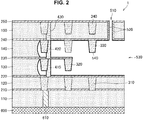
- FIG. 2 is a sectional view illustrating a configuration in which the protective layer 540 is formed on the inner surface of the gap 530 in the semiconductor device 1 illustrated in FIG. 1 .
- the protective layer 540 may be formed on each of the surfaces of the insulating layers 100, the diffusion preventing layers 200, the wiring layers 300, and the through-vias 400 exposed by the gap 530.
- the protective layer 540 includes an arbitrary insulating material, for example, and may include an insulating material such as SiO x , SiN x , SiCN, SiON, SiOC, or SiC, for example. Also, the film thickness of the protective layer 540 may be 2 nm to 50 nm, for example.
- the protective layer 540 can improve reliability of the wirings by preventing electromigration and time dependant dielectric breakdown (TDDB) in the wiring layers 300 and the through-vias 400.
- TDDB time dependant dielectric breakdown
- Such a protective layer 540 can be formed by introducing a raw material gas into the gap 530 via the through-hole 510 and performing an atomic layer deposition (ALD) method, for example.
- ALD atomic layer deposition
- the semiconductor device 1 described above it is possible to form a hollow between the wiring layers 300 by the gap 530 and thereby to reduce the wiring capacity. Therefore, it is possible to realize a high operation speed and low power consumption by suppressing delay in the wirings according to the semiconductor device 1.
- the gap 530 is not provided in the insulating layers 100 (that is, the first insulating layer 110 and the fifth insulating layer 150) provided on the surface of the multilayered wiring layer in the semiconductor device 1, it is possible to maintain mechanical strength of the entire semiconductor device 1. Further since the diffusion preventing layers 200 that protrude into the gap 530 are not generated in the semiconductor device 1, it is possible to prevent the diffusion preventing layers 200 with low mechanical strength from collapsing.
- FIG. 3 is a planar diagram illustrating the semiconductor device 1 according to the embodiment in a plan view in the laminating direction.
- planar arrangement of the second to fourth wiring layers 320, 330, and 340, the through-hole 510, and an opening 231 formed in the third diffusion preventing layer 230 are illustrated and illustration of the other configurations is omitted.
- planar arrangement illustrated in FIG. 3 is just an example, and the planar arrangement of the respective configurations in the semiconductor device 1 according to the embodiment is not limited thereto.
- the second to fourth wiring layers 320, 330, and 340 are formed in mutually different insulating layers 100 as illustrated in FIG. 3 , partial regions thereof are formed in a mutually overlapped manner.
- the first through-via 410 and the second through-via 420 may be formed in the partial regions at which the second to fourth wiring layers 320, 330, and 340 mutually overlapping with each other.
- the through-hole 510 is formed in a region in which the through-hole 510 does not overlap with the third wiring layer 330 and the fourth wiring layer 340 so as not to interfere with the third wiring layer 330 and the fourth wiring layer 340.
- the shape of the opening of the through-hole 510 may be a substantially quadrangular shape with a side of at least 50 nm to 300 nm, for example.
- one through-hole 510 may be provided for one gap 530, or a plurality of through-holes 510 may be provided for one gap 530. Further, the through-hole 510 may be provided in a region for which it is desired to reduce wiring capacity.
- the gap 530 is formed in a region in which the second to fourth wiring layers 320, 330, and 340 are not formed though not illustrated in the drawing.
- the opening 231 formed in the third diffusion preventing layer 230 is formed in a region that avoids the region in which the second wiring layer 320 is formed. This is for preventing the second wiring layer 320 from collapsing by forming the opening 231 since the third diffusion preventing layer 230 is formed on the second wiring layer 320.
- the opening 231 may be formed in a region including a region in which the through-hole 510 is formed or may be formed in a region not including the region in which the through-hole 510 is formed.
- the shape of the opening 231 formed in the third diffusion preventing layer 230 may be an arbitrary polygonal shape with a side of 50 nm to 500 nm.
- FIGS. 4 to 10 are sectional views illustrating steps of the method for manufacturing the semiconductor device 1 according to the embodiment.
- the first insulating layer 110, the first diffusion preventing layer 210, the second insulating layer 120, the second diffusion preventing layer 220, the third insulating layer 130, and the third diffusion preventing layer 230 are sequentially laminated on the substrate 600 provided with the semiconductor element and the like by a CVD method as illustrated in FIG. 4 .
- the contact plug 610, the first wiring layer 310, the second wiring layer 320, and the first through-via 410 are formed in each of the insulating layers 100.
- the first insulating layer 110 is formed on the substrate 600 including silicon (Si) or the like, first.
- the first wiring layer 310 can be formed by using a damascene method in which the first diffusion preventing layer 210 and the second insulating layer 120 are formed on the first insulating layer 110, the first diffusion preventing layer 210 and the second insulating layer 120 in a predetermined region are then removed by etching, and the etched portion is buried again with copper (Cu) or the like.
- the second wiring layer 320 and the first through-via 410 can be formed by a similar method.
- first to third insulating layers 110, 120, and 130 may include SiO x or the like that can be easily etched with a hydrofluoric acid
- first to third diffusion preventing layers 210, 220, and 230 may include SiC or the like with high etching resistance with respect to the hydrofluoric acid.
- the region from which the third diffusion preventing layer 230 has been removed functions as an opening for introducing the etching solution into the second insulating layer 120 in a step of etching the second insulating layer 120 and the third insulating layer 130 in a later stage.
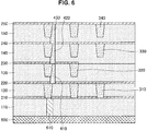
- the fourth insulating layer 140, the fourth diffusion preventing layer 240, the fifth insulating layer 150, and the fifth diffusion preventing layer 250 are sequentially laminated on the third diffusion preventing layer 230 by a CVD method as illustrated in FIG. 6 . Also, the third wiring layer 330, the fourth wiring layer 340, the second through-via 420, and the third through-via 430 are formed on each of the insulating layers 100.
- the third wiring layer 330 it is possible to form the third wiring layer 330 by using the damascene method in which the fourth insulating layer 140 is formed on the third diffusion preventing layer 230, the fourth insulating layer 140 in a predetermined region is then removed by etching, and the etched portion is buried with copper (Cu) or the like.
- the fourth wiring layer 340, the second through-via 420, and the third through-via 430 by a similar method.
- the fourth and fifth insulating layers 140 and 150 may include SiOx or the like that can be easily etched with a hydrofluoric acid
- the fourth and fifth diffusion preventing layers 240 and 250 may include SiC or the like with high etching resistance with respect to the hydrofluoric acid.
- the through-hole 510 is formed by forming a barrier layer 511 on the fifth diffusion preventing layer 250 and removing the fifth insulating layer 150, the fourth diffusion preventing layer 240, and the fifth diffusion preventing layer 250 in a partial region by using etching or the like as illustrated in FIG. 7 .
- the barrier layer 511 functions to protect the fifth diffusion preventing layer 250 and may include SiO 2 of about 100 nm, for example.
- the region in which the through-hole 510 is formed is a region in which the third wiring layer 330 and the fourth wiring layer 340 are not formed, for example, and the shape of the opening of the through hole 510 may be a square shape of 50 nm to 300 nm. Note that a plurality of through-holes 510 may be provided.
- a protective film 521 is formed on the barrier layer 511 and inside the through-hole 510 by using an ALD method as illustrated in FIG. 8 .
- the protective film 521 may be formed to have a film thickness of 5 nm to 30 nm with SiC or the like with high etching resistance with respect to a hydrofluoric acid, for example.
- the protective film 521 is formed by using the ALD method, the protective film 521 is uniformly (conformally) formed on the barrier layer 511 and inside the through-hole 510.
- the protective film 521 is removed while the protective side wall 520 is made to remain inside the through-hole 510 by etching back the entire surface of the protective film 521, thereby causing the barrier layer 511 and the fourth insulating layer 140 to be exposed as illustrated in FIG. 9 .
- Such etching back of the entire surface can be realized by performing etching with significantly high perpendicular anisotropy.
- the gap 530 is formed by introducing a diluted hydrofluoric acid into the second insulating layer 120 and the third insulating layer 130 via the through-hole 510 and performing wet-etching thereon as illustrated in FIG. 10 .
- the barrier layer 511 is removed by the wet etching using the diluted hydrofluoric acid at this time.
- the etching hardly advances through the protective side wall 520 and the second to fourth diffusion preventing layers 220, 230, and 240 since the protective side wall 520 and the second to fourth diffusion preventing layers 220, 230, and 240 include SiC or the like with high etching resistance with respect to the hydrofluoric acid. Also, etching hardly advances through the second wring layer 320, the third wiring layer 330, the first through-via 410, and the second through-via 420 since the second wiring layer 320, the third wiring layer 330, the first through-via 410, and the second through-via 420 include a metal material such as copper (Cu) and have high etching resistance with respect to the hydrofluoric acid.
- Cu copper
- the region in which the gap 530 is formed is controlled depending on a region sandwiched between the second diffusion preventing layer 220 and the fourth diffusion preventing layer 240 in the laminating direction of the semiconductor device 1 and is controlled depending on a time during which the wet etching is performed in the in-plane direction of the semiconductor device 1.
- the third diffusion preventing layer 230 is formed in a region with an end corresponding to a region in which the second wiring layer 320 is formed and does not protrude to the gap 530, it is possible to prevent the third diffusion preventing layer 230 from collapsing.
- a sealing layer that includes an insulating material and blocks the opening of the through-hole 510 may be provided on the fifth diffusion preventing layer 250 in order to prevent moisture and the like from entering the gap 530.
- the hydrofluoric acid is used for the etching
- SiO x is used as a material that can be easily etched with respect to the hydrofluoric acid for the insulating layers 100
- SiC is used as a material with high etching resistance with respect to the hydrofluoric acid for the diffusion preventing layers 200.
- the technology according to the present disclosure is not limited to the aforementioned illustrative example.
- An arbitrary combination may be employed as a combination of materials used for the insulating layers 100 and the diffusion preventing layers 200 as long as it is possible to secure a sufficient etching selection ratio.
- FIG. 11 is a sectional view illustrating a semiconductor device 1A according to a first modification example of the embodiment taken along the laminating direction
- FIG. 12 is a sectional view illustrating a semiconductor device 1B according to a second modification example of the embodiment taken along the laminating direction
- FIG. 13 is a sectional view illustrating a semiconductor device 1C according to a third modification example of the embodiment taken along the laminating direction. Note that it is needless to say that FIGS. 11 to 13 illustrate parts of the sectional surfaces of the semiconductor devices and the semiconductor devices also extend in the in-plane direction in ranges that are not illustrated in the drawings.
- the semiconductor device 1A according to the first modification example of the embodiment will be described with reference to FIG. 11 .
- the semiconductor device 1A includes a multilayered wiring layer in which six insulating layers 100 and six diffusion preventing layers 200 are alternately laminated and is different from the semiconductor device 1 as illustrated in FIG. 1 in that a gap 530A is formed in the fifth insulating layer 150.
- a sixth insulating layer 160 may include a material similar to that of the first to fifth insulating layers 110, 120, 130, 140, and 150
- the sixth diffusion preventing layer 260 may include a material similar to that of the first to fifth diffusion preventing layers 210, 220, 230, 240, and 250.
- the description thereof will be omitted here.
- a gap 530A may be formed only in one insulating layer 100 (that is, the fifth insulating layer 150). At this time, since no opening is formed in the fourth diffusion preventing layer 240 provided below the fifth insulating layer 150 by etching, the etching solution does not enter the fourth insulating layer 140, and the gap 530A is not formed in the fourth insulating layer 140. In the semiconductor device 1A according to the first modification example, a space in which the gap 530A is formed is reduced, it is possible to improve mechanical strength of the entire semiconductor device 1A.
- the semiconductor device 1A according to the first modification example may include a multilayered wiring layer in which six insulating layers 100 and six diffusion preventing layers 200 are alternately laminated or may include a multilayered wiring layer in which seven or more insulating layers 100 and seven or more diffusion preventing layers 200 are alternately laminated.
- the number of layers laminated in the multilayered wiring layer that forms the semiconductor device 1 may be at least three or more in order to form the gap 530 inside the multilayered wiring layer, and an upper limit thereof is not particularly limited.
- the semiconductor device 1B is different from the semiconductor device 1 as illustrated in FIG. 1 in that a through-hole 510B is formed to penetrate through the fourth and fifth insulating layers 140 and 150 and the third to fifth diffusion preventing layers 230, 240, and 250. Therefore, the gap 530 is formed in the second insulating layer 120 and the third insulating layer 130 in the semiconductor device 1B. Note that since the respective configurations in the semiconductor device 1B are as described above with reference to FIG. 1 , description thereof will be omitted here.
- the through-hole 501B may be provided to penetrate through the plurality of insulating layers 100 (that is, the fourth insulating layer 140 and the fifth insulating layer 150).
- the opening is formed in the second diffusion preventing layer 220 and the etching solution for forming the gap 530 enters the second insulating layer 120 from the third insulating layer 130, the gap 530 is formed in the second insulating layer 120 and the third insulating layer 130. Since the gap 530 is formed in the third and following layers from the surface of the multilayered wiring layer in the semiconductor device 1B according to the second modification example, it is possible to improve mechanical strength of the entire semiconductor device 1B.
- the through-hole 510B may be provided to further penetrate through three or more insulating layers 100 in the semiconductor device 1B according to the second modification example.
- the number of the insulating layers 100 through which the through-hole 510B penetrates may be four or less, for example.
- the semiconductor device 1C is different from the semiconductor device 1 illustrated in FIG. 1 in that a gap 530C is formed in the second to fourth insulating layers 120, 130, and 140. Note that since the respective configurations in the semiconductor device 1C are as described above with reference to FIG. 1 , description thereof will be omitted here.
- the gap 530C may be further formed over the three or more insulating layers 100 other than the insulating layers 100 on the surface of the multilayered wiring layer (that is, the first insulating layer 110 and the fifth insulating layer 150) that forms the semiconductor device 1C.
- the etching solution enters the second insulating layer 120 and the third insulating layer 130, and the gap 530C is formed from the second insulating layer 120 to the fourth insulating layer 140.
- the gap 530C may be further provided in a plurality of insulating layers 100 in the semiconductor device 1C according to the third modification example.
- the number of the insulating layers 100 in which the gap 530C is formed may be 5 or less, for example.
- FIG. 14 is a sectional view of a semiconductor device 2 according to the embodiment taken in a laminating direction. Note that FIG. 14 illustrates a part of the sectional surface of the semiconductor device 2 and it is needless to say that the semiconductor device 2 also extends in an in-plane direction in a range which is not illustrated in the drawing.
- the multilayered wiring layer in which the insulating layers 100 and the diffusion preventing layers 200 are alternately laminated is sandwiched between a pair of substrates 600 and 620 in the semiconductor device 2, and the through-hole 510 is provided to penetrate through the substrate 600 and the first insulating layer 110.
- the semiconductor device 2 illustrated in FIG. 14 is obtained by vertically inverting the semiconductor device 1 illustrated in FIG. 1 .
- a sixth insulating layer 160 and a seventh insulating layer 170 may include a material similar to that of the first to fifth insulating layers 110, 120, 130, 140, and 150
- the sixth diffusion preventing layer 260 may include a material similar to that of the first to fifth diffusion preventing layers 210, 220, 230, 240, and 250.
- the description thereof will be omitted here.
- the semiconductor device 2 it is possible to improve mechanical strength of the entire semiconductor device 2 by sandwiching the multilayered wiring layer in which the insulating layers 100 and the diffusion preventing layers 200 are alternately laminated between the pair of substrates 600 and 620.
- a substrate of any material can be used as the substrate 620 as long as it is possible to bond the substrate 620 to the multilayered wiring layer in which the insulating layers 100 and the diffusion preventing layers 200 are alternately laminated.
- the substrate 620 may be a substrate including glass such as quartz, resin such as polyimide or polyester, or a semiconductor of silicone (Si) or the like, for example.
- the thickness of the substrate 600 with the semiconductor element (not illustrated) formed thereon may be reduced by using chemical mechanical polishing (CMP) or the like.
- CMP chemical mechanical polishing
- the semiconductor element provided on the substrate 600 is a color sensor
- such a semiconductor device 2 can be used as an image pickup device of a rear surface irradiation type, for example.
- the through-hole 510 may be provided in the insulating layer 100 on any of the surfaces of the multilayered wiring layer in which the insulating layers 100 and the diffusion preventing layers 200 are alternately laminated. That is, the through-hole 510 may be provided in the first insulating layer 110 or may be provided in the seventh insulating layer 170. It is also possible to form the gap 530 inside the multilayered wiring layer via the through-hole 510 similarly to the first embodiment in the semiconductor device 2 in such a case.
- FIGS. 15 to 21 are sectional views illustrating steps of the method for manufacturing the semiconductor device 2 according to the embodiment.
- the first insulating layer 110, the first diffusion preventing layer 210, the second insulating layer 120, and the second diffusion preventing layer 220 are sequentially laminated on the substrate 600 with the semiconductor element and the like provided thereon by the CVD method as illustrated in FIG. 15 . Also, the contact plug 610 is formed on the first insulating layer 110, and the first wiring layer 310 is formed on the second insulating layer 120.
- the first insulating layer 110 is formed on the substrate 600 including silicon (Si) or the like, first.
- the first wiring layer 310 can be formed by using a damascene method in which the first diffusion preventing layer 210 and the second insulating layer 120 are formed on the first insulating layer 110, the first diffusion preventing layer 210 and the second insulating layer 120 in a predetermined region are then removed by etching, and the etched portion is buried again with copper (Cu) or the like.
- first and second insulating layers 110 and 120 may include SiO x or the like that can be easily etched with a hydrofluoric acid
- first and second diffusion preventing layers 210 and 220 may include SiC or the like with high etching resistance with respect to the hydrofluoric acid.
- the region from which the second diffusion preventing layer 220 has been removed functions as an opening for introducing the etching solution into the third insulating layer 130 in a step of etching the second insulating layer 120 and the third insulating layer 130 in a later stage.
- the third insulating layer 130, the third diffusion preventing layer 230, the fourth insulating layer 140, the fourth diffusion preventing layer 240, the fifth insulating layer 150, and the fifth diffusion preventing layer 250 are sequentially laminated on the second diffusion preventing layer 220 by a CVD method as illustrated in FIG. 17 .
- the second wiring layer 320, the third wiring layer 330, the fourth wiring layer 340, the first through-via 410, the second through-via 420, and the third through-via 430 are formed on each of the insulating layers 100.
- the second wiring layer 320 by using the damascene method in which the third insulating layer 130 is formed on the second diffusion preventing layer 220, the third insulating layer 130 in a predetermined region is then removed by etching, and the etched portion is buried with copper (Cu) or the like.
- the third wiring layer 330, the fourth wiring layer 340, the first through-via 410, the second through-via 420, and the third through-via 430 by a similar method.
- the third to fifth insulating layers 130, 140, and 150 may include SiOx or the like that can be easily etched with a hydrofluoric acid, and the third to fifth diffusion preventing layers 230, 240, and 250 may include SiC or the like with high etching resistance with respect to the hydrofluoric acid.
- the sixth insulating layer 160, the sixth diffusion preventing layer 260, and the seventh insulating layer 170 are laminated on the fifth diffusion preventing layer 250 by the CVD method, and the substrate 620 is then bonded to the surface of the seventh insulating layer 170 as illustrated in FIG. 18 .
- the thickness of the substrate 600 may be reduced by CMP or the like after the substrate 620 is bonded to the multilayered wiring layer.
- the sixth and seventh insulating layers 160 and 170 may include SiOx or the like that can be easily etched with a hydrofluoric acid, and the sixth diffusion preventing layer 260 may include SiC or the like with high etching resistance with respect to the hydrofluoric acid.
- the substrate 620 may be a silicon (Si) substrate.
- the through-hole 510 may be formed by removing the first insulating layer 110, the first diffusion preventing layer 210, and the substrate 600 in a partial region by using etching or the like as illustrated in FIG. 19 .
- the protective film 521 is formed on the substrate 600 and inside the through-hole 510.
- the shape of the opening of the through-hole 510 may be a square shape with a side of 50 nm to 300 nm, and a plurality of through-holes 510 may be provided.
- the protective film 521 may be formed to have a film thickness of 5 nm to 30 nm by using SiC or the like with high etching resistance with respect to the hydrofluoric acid, for example.
- the protective film 521 is formed by using the ALD method, the protective film 521 is uniformly (conformally) formed on the substrate 600 and inside the through-hole 510.
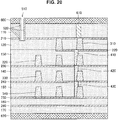
- the substrate 600 and the second insulating layer 120 are exposed by removing the protective film 521 while causing the protective side wall 520 to remain inside the through-hole 510 by etching back the entire surface of the protective film 521 as illustrated in FIG. 20 .
- Such etching back of the entire surface can be realized by performing etching with high perpendicular anisotropy, for example.
- the gap 530 is formed by introducing a diluted hydrofluoric acid into the second insulating layer 120 and the third insulating layer 130 via the through-hole 510 and performing wet watching as illustrated in FIG. 21 .
- the etching hardly advances through the protective side wall 520 and the first to third diffusion preventing layers 210, 220, and 230 since the protective side wall 520 and the first to third diffusion preventing layers 210, 220, and 230 include SiC or the like with high etching resistance with respect to the hydrofluoric acid. Also, etching hardly advances through the first wiring layer 310, the second wring layer 320, and the first through-via 410 since the first wiring layer 310, the second wiring layer 320, and the first through-via 410 include a metal material such as copper (Cu) and have high etching resistance with respect to the hydrofluoric acid.
- Cu copper
- the region in which the gap 530 is formed is controlled depending on a region sandwiched between the first diffusion preventing layer 210 and the third diffusion preventing layer 230 in the laminating direction of the semiconductor device 2 and is controlled depending on a time during which the wet etching is performed in the in-plane direction of the semiconductor device 2.
- a sealing layer that includes an insulating material and blocks the opening of the through-hole 510 may be provided on the substrate 600 in order to prevent moisture and the like from entering the gap 530.
- the gap 530 is formed inside the semiconductor device 2 after the thickness of the substrate 600 is reduced by the CMP. According to this, it is possible to suppress occurrence of cracking or the like in the CMP process since the gap 530 is formed in the semiconductor device 2 after the CMP process in which mechanical stress is applied.
- the gap 530 is not provided in the insulating layers 100 provided on the surface of the multilayered wiring layer in the semiconductor device, it is possible to maintain mechanical strength of the entire semiconductor device. Further since the diffusion preventing layers 200 that protrude into the gap 530 are not generated in the semiconductor device, it is possible to prevent the diffusion preventing layers 200 with low mechanical strength from collapsing.
- the semiconductor device of the embodiment of the present disclosure it is possible to use the semiconductor device in a memory device, a logic circuit, or an image pickup device, for example, by changing semiconductor elements to be mounted thereon.
- the semiconductor device 2 according to the second embodiment of the present disclosure as an image pickup device of a rear surface irradiation type by mounting a color sensor as a semiconductor element.
- present technology may also be configured as below.
Landscapes
- Internal Circuitry In Semiconductor Integrated Circuit Devices (AREA)
- Solid State Image Pick-Up Elements (AREA)
- Chemical & Material Sciences (AREA)
- Chemical Kinetics & Catalysis (AREA)
- General Chemical & Material Sciences (AREA)
Abstract
Description
- The present invention relates to a semiconductor device, an image pickup device, and a method for manufacturing a semiconductor device.
- In recent years, with the miniaturization of semiconductor devices, signal delay due to wiring has attracted attention as a factor reducing an operation speed of a semiconductor device. Specifically, since a sectional area of the wiring decreases due to the miniaturization of the semiconductor device, and a wiring resistance increases, delay in proportion to a product between the wiring resistance and wiring capacity (also referred to as RC delay) increases.
- In order to reduce such signal delay due to wiring, causing an interlayer film between wirings to have a lower dielectric constant has been considered. However, an interlayer film material that realizes a sufficiently low dielectric constant has not been found yet.
- Thus, further reducing the dielectric constant between wirings by removing the material between the wirings and providing a hollow layer (also referred to as an air gap) with a specific
dielectric constant 1 between the wirings has been considered. - For example,
Patent Literature 1 listed below discloses providing a structure that does not damage wirings when insulating layers between wirings are removed to form an air gap structure. - Patent Literature 1:
JP 2006-19401A - However, since a thin film with low mechanical strength protrudes into a space in which the air gap is formed according to the technology disclosed in
Patent Literature 1, there is a probability that the protruding thin film may collapse. Also, since mechanical strength of an entire semiconductor device is degraded due to the air gap in a case in which intervals between the wirings are wide according to the technology disclosed inPatent Literature 1, there is a probability that reliability of the semiconductor device will be degraded. - Thus, the present disclosure proposes a novel and improved semiconductor device, an image pickup device, and a method for manufacturing the semiconductor device capable of reducing wiring capacity by using gaps and maintaining mechanical strength and reliability.
- According to the present disclosure, there is provided a semiconductor device including: a multilayered wiring layer in which insulating layers and diffusion preventing layers are alternately laminated and a wiring layer is provided inside; a through-hole that is provided to penetrate through at least one or more insulating layers from one surface of the multilayered wiring layer and has an inside covered with a protective side wall; and a gap that is provided in at least one or more insulating layers immediately below the through-hole.
- In addition, according to the present disclosure, there is provided an image pickup device including: a multilayered wiring layer in which insulating layers and diffusion preventing layers are alternately laminated and a wiring layer is provided inside; a through-hole that is provided to penetrate through at least one or more insulating layers from one surface of the multilayered wiring layer and has an inside covered with a protective side wall; and a gap that is provided in at least one or more insulating layers immediately below the through-hole.
- In addition, according to the present disclosure, there is provided a method for manufacturing a semiconductor device, including: a step of forming a multilayered wiring layer in which insulating layers and diffusion preventing layers are alternately laminated and a wiring layer is provided inside; a step of forming a through-hole such that the through-hole penetrates through at least one or more insulating layers from one surface of the multilayered wiring layer; a step of forming a protective side wall inside the through-hole; and a step of forming a gap by etching at least one or more insulating layers immediately below the through-hole.
- According to the present disclosure, it is possible to form gaps in insulating layers that are the second and following layers from a surface of the multilayered wiring layer that forms a semiconductor device. According to this, since it is possible to provide a hollow with a specific
dielectric constant 1 between wirings while the mechanical strength of the semiconductor device is maintained, it is possible to reduce wiring capacity of the semiconductor device. - According to the present disclosure, it is possible to reduce wiring capacity by the gaps and to maintain mechanical strength and reliability of the semiconductor device.
- Note that the effects described above are not necessarily limitative. With or in the place of the above effects, there may be achieved any one of the effects described in this specification or other effects that may be grasped from this specification.
-
-
FIG. 1 is a sectional view of a semiconductor device according to a first embodiment of the present disclosure taken in a laminating direction. -
FIG. 2 is a sectional view illustrating a configuration in which a protective layer is formed in a surface inside a gap in the semiconductor device illustrated inFIG. 1 . -
FIG. 3 is a planar diagram of the semiconductor device according to the embodiment in a plan view in the laminating direction. -
FIG. 4 is a sectional view illustrating a step of a method for manufacturing the semiconductor device according to the embodiment. -
FIG. 5 is a sectional view illustrating a step of a method for manufacturing the semiconductor device according to the embodiment. -
FIG. 6 is a sectional view illustrating a step of a method for manufacturing the semiconductor device according to the embodiment. -
FIG. 7 is a sectional view illustrating a step of a method for manufacturing the semiconductor device according to the embodiment. -
FIG. 8 is a sectional view illustrating a step of a method for manufacturing the semiconductor device according to the embodiment. -
FIG. 9 is a sectional view illustrating a step of a method for manufacturing the semiconductor device according to the embodiment. -
FIG. 10 is a sectional view illustrating a step of a method for manufacturing the semiconductor device according to the embodiment. -
FIG. 11 is a sectional view illustrating a semiconductor device according to a first modification example taken in a laminating direction. -
FIG. 12 is a sectional view illustrating a semiconductor device according to a second modification example taken in a laminating direction. -
FIG. 13 is a sectional view illustrating a semiconductor device according to a third modification example taken in a laminating direction. -
FIG. 14 is a sectional view illustrating a semiconductor device according to a second embodiment of the present disclosure taken in a laminating direction. -
FIG. 15 is a sectional view illustrating a step of a method for manufacturing the semiconductor device according to the embodiment. -
FIG. 16 is a sectional view illustrating a step of a method for manufacturing the semiconductor device according to the embodiment. -
FIG. 17 is a sectional view illustrating a step of a method for manufacturing the semiconductor device according to the embodiment. -
FIG. 18 is a sectional view illustrating a step of a method for manufacturing the semiconductor device according to the embodiment. -
FIG. 19 is a sectional view illustrating a step of a method for manufacturing the semiconductor device according to the embodiment. -
FIG. 20 is a sectional view illustrating a step of a method for manufacturing the semiconductor device according to the embodiment. -
FIG. 21 is a sectional view illustrating a step of a method for manufacturing the semiconductor device according to the embodiment. - Hereinafter, (a) preferred embodiment(s) of the present disclosure will be described in detail with reference to the appended drawings. Note that, in this specification and the appended drawings, structural elements that have substantially the same function and structure are denoted with the same reference numerals, and repeated explanation of these structural elements is omitted.
- Note that description will be given in the following order.
- 1. First embodiment
- 1.1. Sectional structure of semiconductor device
- 1.2. Planar structure of semiconductor device
- 1.3. Method for manufacturing semiconductor device
- 1.4. Modification examples
- 2. Second embodiment
- 2.1. Sectional structure of semiconductor device
- 2.2. Method for manufacturing semiconductor device
- 3. Conclusion
- First, a sectional structure of a semiconductor device according to a first embodiment of the present disclosure will be described with reference to
FIG. 1. FIG. 1 is a sectional view of asemiconductor device 1 according to the embodiment taken in a laminating direction. Note thatFIG. 1 illustrates a part of the sectional surface of thesemiconductor device 1 according to the embodiment and it is needless to say that thesemiconductor device 1 also extends in an in-plane direction in a range which is not illustrated in the drawing. - As illustrated in
FIG. 1 , thesemiconductor device 1 includes asubstrate 600 and a multilayered wiring layer in which first to fifth insulatinglayers diffusion preventing layers substrate 600 is provided with a semiconductor element (not illustrated), and the second to fifth insulatinglayers first wiring layer 310 via acontact plug 610, and the first to fourth wiring layers 310, 320, 330, and 340 are caused to have continuity with each other via first to third through-vias - In the following description, the first to fifth insulating
layers diffusion preventing layers vias - That is, the
semiconductor device 1 includes the multilayered wiring layer in which the insulating layers 100 including the wiring layers 300 and the through-vias 400 and the diffusion preventing layers 200 are alternately laminated. - Note that, although
FIG. 1 illustrates that thesemiconductor device 1 has a configuration of a five-layer structure in which the first to fifth insulatinglayers diffusion preventing layers semiconductor device 1 may include a multilayered wiring layer including three or four layers or may include a multilayered wiring layer including six or more layers. - The insulating layers 100 are main layer formation materials that electrically insulate the wiring layers 300 from each other and form the
semiconductor device 1. The insulating layers 100 include an insulating material that can be etched relatively easily (specifically, that can be etched more easily than the diffusion preventing layers 200, which will be described layer) and may include an insulating material such as SiOx, for example. - The diffusion preventing layers 200 are provided to sandwich the respective insulating layers 100, suppress surface diffusion of metal atoms that form the wiring layers 300, and serve as stoppers when members in the upper layers are worked. Specifically, the diffusion preventing layers 200 include an insulating material with higher etching resistance (for example, etching resistance with respective to fluorine compounds) than the insulating layers 100 and may include an insulating material such as SiNx, SiCN, SiON, or SiC, for example.
- The wiring layers 300 deliver currents or voltages between the respective elements provided in the
semiconductor device 1. The wiring layers 300 include a conductive metal material and may include copper (Cu), tungsten (W), aluminum (Al), or an alloy containing these metals, for example. Also, barrier metal layers may be formed using a metal with a high barrier property on the surfaces of the wiring layers 300, although these are not illustrated in the drawing. The barrier metal layer can include a metal such as tantalum (Ta), titanium (Ti), ruthenium (Ru), cobalt (Co), or manganese (Mn) or nitrides or oxides of these metals, for example. - The through-vias 400 electrically connect the wiring layers 300 provided in different insulating layers 100. Specifically, the first through-via 410 connects the
first wiring layer 310 to thesecond wiring layer 320, the second through-via 420 connects thesecond wiring layer 320 to thethird wiring layer 330, and the third through-via 430 connects thethird wiring layer 330 to thefourth wiring layer 340. The through-vias 400 include a conductive metal material similarly to the wiring layers 300 and may include copper (Cu), tungsten (W), aluminum (Al), or an alloy containing these materials, for example. Also, barrier metal layers may be formed on the surfaces of the through-vias 400 similarly to the wiring layers 300. - The
substrate 600 is a substrate including various semiconductors and may be a substrate including polycrystalline, monocrystalline, or amorphous silicon (Si). Also, thesubstrate 600 is provided with a semiconductor element that realizes functions of thesemiconductor device 1. As the semiconductor element provided on thesubstrate 600, a logic circuit or the like including a memory element, a color sensor, or a transistor, for example, can be exemplified. - The
contact plug 610 electrically connects an electrode or a wiring of the semiconductor element or the like provided on thesubstrate 600 to thefirst wiring layer 310. Thecontact plug 610 may include a metal material that is similar to that of the through-vias 400 and may include copper (Cu), tungsten (W), aluminum (Al), or an alloy containing these metals, for example. - In addition, the
semiconductor device 1 is provided with a through-hole 510 that penetrates the fifthdiffusion preventing layer 250, the fifth insulatinglayer 150, and the fourthdiffusion preventing layer 240 and has an inside covered with aprotective side wall 520, as illustrated inFIG. 1 . The through-hole 510 causes agap 530 provided at the third insulatinglayer 130 and the fourth insulatinglayer 140 to communicate with an external space. - Note that a sealing layer that blocks an opening of the through-
hole 510 may be provided on the fifthdiffusion preventing layer 250 although this is not illustrated inFIG. 1 . The sealing layer includes an arbitrary insulating material such as SiOx, SiNx, SiCN, SiON, or SiC, for example and prevents moisture and the like from entering the through-hole 510 and thegap 530. - The through-
hole 510 is provided to penetrate through the insulating layer 100 provided on any one surface of thesemiconductor device 1 and the diffusion preventing layers 200 that sandwich the insulating layer 100. Specifically, the through-hole 510 is provided to penetrate through the fifth insulatinglayer 150, and the fourthdiffusion preventing layer 240 and the fifthdiffusion preventing layer 250 that sandwich the fifth insulatinglayer 150 therebetween. The shape of the opening of the through-hole 510 may be a substantially quadrangular shape with a side of at least 50 nm to 300 nm or may be a substantially circular shape with a diameter of 50 nm to 300 nm, for example. - The
protective side wall 520 is provided inside the through-hole 510 to protect a side surface of the fifth insulatinglayer 150 exposed due to the through-hole 510. Theprotective side wall 520 includes an insulating material with higher etching resistance (for example, etching resistance with respect to fluorine compounds) than that of the insulating layers 100, for example, and may include an insulating material such as SiNx, SiCN, SiON, SiOC, or SiC, for example. - The
protective side wall 520 functions to protect the fifth insulatinglayer 150 such that the fifth insulatinglayer 150 is not etched when thegap 530 is formed. Specifically, thegap 530 is formed by introducing an etching solution via the through-hole 510 and performing wet-etching on the third insulatinglayer 130 and the fourth insulatinglayer 140. At this time, theprotective side wall 520 prevents the fifth insulatinglayer 150 from being wet-etched by the etching solution. Therefore, it is possible to form thegap 530 in the insulating layer 100 provided inside the second and following layers in the multilayered wiring layer in thesemiconductor device 1 by using the through-hole 510 with the inside covered with theprotective side wall 520. Note that theprotective side wall 520 may be a thin film of 5 nm to 30 nm, for example. - The
gap 530 is provided in the second and following insulating layers 100 in the multilayered wiring layer (that is, the inside of the multilayered wiring layer) in thesemiconductor device 1, and spaces in the wiring layers 300 are formed as hollows with a specific dielectric constant of 1. In this manner, thegap 530 can reduce wiring capacity in the wiring layers 300. Specifically, thegap 530 is provided at the third insulatinglayer 130 and the fourth insulatinglayer 140 and can reduce the wiring capacity by forming the space between thethird wiring layer 330 and thesecond wiring layer 320 as a hollow. - Note that the
gap 530 is not provided in the insulating layer 100 on the surface of the multilayered wiring layer in thesemiconductor device 1. Specifically, thegap 530 is not provided in the first insulatinglayer 110 and the fifth insulatinglayer 150 on the surface of the multilayered wiring layer. In this manner, it is possible to maintain overall mechanical strength although thegap 530 is formed in thesemiconductor device 1. - The
gap 530 can be formed by introducing an etching solution via the through-hole 510 and performing etching on the third insulatinglayer 130 and the fourth insulatinglayer 140 by using a wet etching method. - At this time, a region in which the
gap 530 is formed is restricted to a region surrounded by the diffusion preventing layers 200 in the laminating direction of the multilayered wiring layer. This is because it is difficult for etching to advance through the diffusion preventing layers 200 due to higher etching resistance thereof than that of the insulating layers 100. Therefore, in a case in which sufficient etching is performed, thegap 530 causes the seconddiffusion preventing layer 220 and the fourthdiffusion preventing layer 240 that are present above and below the third insulatinglayer 130 and the fourth insulatinglayer 140 to be exposed. - In addition, the region in which the
gap 530 is formed is controlled by a length of time during which etching is performed in the in-plane direction of the multilayered wiring layer. That is, thegap 530 is formed in a region that extends isotropically from a portion immediately below the through-hole 510 into which the etching solution has been introduced while the broadness of the region is controlled by an etching time. - Note that the through-vias 400 or the wiring layers 300 are not etched under conditions under which the insulating layers 100 are etched. Therefore, in a case in which the through-vias 400 or the wiring layers 300 are present in the region in which the
gap 530 is formed, the through-vias 400 or the wiring layers 300 directly remain inside thegap 530. Also, in a case in which the insulating layers 100 are spatially sectioned by the through-vias 400 or the wiring layers 300, the etching solution does not enter a space on the opposite side sectioned by the through-vias 400 or the wiring layers 300. In this case, the region in which thegap 530 is formed is restricted by the through-vias 400 or the wiring layers 300. - In a case in which the
gap 530 is provided in a plurality of insulating layers 100, a part of the diffusion preventing layers 200 between the plurality of insulating layers 100 is removed in advance to form an opening. Specifically, thegap 530 is provided in the third insulatinglayer 130 and the fourth insulatinglayer 140, and a part of the thirddiffusion preventing layer 230 in the vicinity of the through-hole 510 is removed in advance to form an opening. In this manner, since the etching solution can be diffused from the fourth insulatinglayer 140 to the third insulatinglayer 130 when the etching for forming thegap 530 is performed, it is possible to form thegap 530 over a plurality of layers, namely the third insulatinglayer 130 and the fourth insulatinglayer 140. - In addition, an opening is formed at this time in the diffusion preventing layers 200 such that a region that protrudes to the
gap 530 and is not formed above the wiring layer 300 is not formed. In this manner, it is possible to prevent the diffusion preventing layers 200 protruding to thegap 530 from collapsing after thegap 530 is formed. - Note that, although
FIG. 1 illustrates a case in which only one through-hole 510 is formed, the technology according to the present disclosure is not limited to the aforementioned illustrative example. For example, a plurality of through-holes 510 may be formed. In such a case, the plurality of through-holes 510 may form thesame gap 530 or each may form aseparate gap 530. - In addition, the
protective layer 540 may be formed on the surface exposed by thegap 530 as illustrated inFIG. 2. FIG. 2 is a sectional view illustrating a configuration in which theprotective layer 540 is formed on the inner surface of thegap 530 in thesemiconductor device 1 illustrated inFIG. 1 . - As illustrated in
FIG. 2 , theprotective layer 540 may be formed on each of the surfaces of the insulating layers 100, the diffusion preventing layers 200, the wiring layers 300, and the through-vias 400 exposed by thegap 530. - The
protective layer 540 includes an arbitrary insulating material, for example, and may include an insulating material such as SiOx, SiNx, SiCN, SiON, SiOC, or SiC, for example. Also, the film thickness of theprotective layer 540 may be 2 nm to 50 nm, for example. Theprotective layer 540 can improve reliability of the wirings by preventing electromigration and time dependant dielectric breakdown (TDDB) in the wiring layers 300 and the through-vias 400. Such aprotective layer 540 can be formed by introducing a raw material gas into thegap 530 via the through-hole 510 and performing an atomic layer deposition (ALD) method, for example. - According to the
semiconductor device 1 described above, it is possible to form a hollow between the wiring layers 300 by thegap 530 and thereby to reduce the wiring capacity. Therefore, it is possible to realize a high operation speed and low power consumption by suppressing delay in the wirings according to thesemiconductor device 1. - In addition, since the
gap 530 is not provided in the insulating layers 100 (that is, the first insulatinglayer 110 and the fifth insulating layer 150) provided on the surface of the multilayered wiring layer in thesemiconductor device 1, it is possible to maintain mechanical strength of theentire semiconductor device 1. Further since the diffusion preventing layers 200 that protrude into thegap 530 are not generated in thesemiconductor device 1, it is possible to prevent the diffusion preventing layers 200 with low mechanical strength from collapsing. - Next, an example of planar arrangement of the respective configurations in the
semiconductor device 1 according to the embodiment will be described with reference toFIG. 3. FIG. 3 is a planar diagram illustrating thesemiconductor device 1 according to the embodiment in a plan view in the laminating direction. - Note that only the planar arrangement of the second to fourth wiring layers 320, 330, and 340, the through-
hole 510, and anopening 231 formed in the thirddiffusion preventing layer 230 are illustrated and illustration of the other configurations is omitted. Also, the planar arrangement illustrated inFIG. 3 is just an example, and the planar arrangement of the respective configurations in thesemiconductor device 1 according to the embodiment is not limited thereto. - Since the second to fourth wiring layers 320, 330, and 340 are formed in mutually different insulating layers 100 as illustrated in
FIG. 3 , partial regions thereof are formed in a mutually overlapped manner. Also, the first through-via 410 and the second through-via 420, for example, may be formed in the partial regions at which the second to fourth wiring layers 320, 330, and 340 mutually overlapping with each other. - The through-
hole 510 is formed in a region in which the through-hole 510 does not overlap with thethird wiring layer 330 and thefourth wiring layer 340 so as not to interfere with thethird wiring layer 330 and thefourth wiring layer 340. The shape of the opening of the through-hole 510 may be a substantially quadrangular shape with a side of at least 50 nm to 300 nm, for example. Also, one through-hole 510 may be provided for onegap 530, or a plurality of through-holes 510 may be provided for onegap 530. Further, the through-hole 510 may be provided in a region for which it is desired to reduce wiring capacity. - The
gap 530 is formed in a region in which the second to fourth wiring layers 320, 330, and 340 are not formed though not illustrated in the drawing. - The
opening 231 formed in the thirddiffusion preventing layer 230 is formed in a region that avoids the region in which thesecond wiring layer 320 is formed. This is for preventing thesecond wiring layer 320 from collapsing by forming theopening 231 since the thirddiffusion preventing layer 230 is formed on thesecond wiring layer 320. In addition, theopening 231 may be formed in a region including a region in which the through-hole 510 is formed or may be formed in a region not including the region in which the through-hole 510 is formed. Note that the shape of theopening 231 formed in the thirddiffusion preventing layer 230 may be an arbitrary polygonal shape with a side of 50 nm to 500 nm. - Next, a method for manufacturing the
semiconductor device 1 according to the embodiment will be described with reference toFIGS. 4 to 10. FIGS. 4 to 10 are sectional views illustrating steps of the method for manufacturing thesemiconductor device 1 according to the embodiment. - First, the first insulating
layer 110, the firstdiffusion preventing layer 210, the second insulatinglayer 120, the seconddiffusion preventing layer 220, the third insulatinglayer 130, and the thirddiffusion preventing layer 230 are sequentially laminated on thesubstrate 600 provided with the semiconductor element and the like by a CVD method as illustrated inFIG. 4 . In addition, thecontact plug 610, thefirst wiring layer 310, thesecond wiring layer 320, and the first through-via 410 are formed in each of the insulating layers 100. - Specifically, the first insulating
layer 110 is formed on thesubstrate 600 including silicon (Si) or the like, first. Next, thefirst wiring layer 310 can be formed by using a damascene method in which the firstdiffusion preventing layer 210 and the second insulatinglayer 120 are formed on the first insulatinglayer 110, the firstdiffusion preventing layer 210 and the second insulatinglayer 120 in a predetermined region are then removed by etching, and the etched portion is buried again with copper (Cu) or the like. In addition, thesecond wiring layer 320 and the first through-via 410 can be formed by a similar method. - Note that the first to third insulating
layers diffusion preventing layers - Next, a part of the third
diffusion preventing layer 230 is removed by using a photolithography method as illustrated inFIG. 5 . At this time, the region from which the thirddiffusion preventing layer 230 has been removed functions as an opening for introducing the etching solution into the second insulatinglayer 120 in a step of etching the second insulatinglayer 120 and the third insulatinglayer 130 in a later stage. - Next, the fourth insulating
layer 140, the fourthdiffusion preventing layer 240, the fifth insulatinglayer 150, and the fifthdiffusion preventing layer 250 are sequentially laminated on the thirddiffusion preventing layer 230 by a CVD method as illustrated inFIG. 6 . Also, thethird wiring layer 330, thefourth wiring layer 340, the second through-via 420, and the third through-via 430 are formed on each of the insulating layers 100. - Specifically, it is possible to form the
third wiring layer 330 by using the damascene method in which the fourth insulatinglayer 140 is formed on the thirddiffusion preventing layer 230, the fourth insulatinglayer 140 in a predetermined region is then removed by etching, and the etched portion is buried with copper (Cu) or the like. In addition, it is possible to form thefourth wiring layer 340, the second through-via 420, and the third through-via 430 by a similar method. Note that the fourth and fifth insulatinglayers diffusion preventing layers - Next, the through-
hole 510 is formed by forming abarrier layer 511 on the fifthdiffusion preventing layer 250 and removing the fifth insulatinglayer 150, the fourthdiffusion preventing layer 240, and the fifthdiffusion preventing layer 250 in a partial region by using etching or the like as illustrated inFIG. 7 . Thebarrier layer 511 functions to protect the fifthdiffusion preventing layer 250 and may include SiO2 of about 100 nm, for example. Also, the region in which the through-hole 510 is formed is a region in which thethird wiring layer 330 and thefourth wiring layer 340 are not formed, for example, and the shape of the opening of the throughhole 510 may be a square shape of 50 nm to 300 nm. Note that a plurality of through-holes 510 may be provided. - Next, a
protective film 521 is formed on thebarrier layer 511 and inside the through-hole 510 by using an ALD method as illustrated inFIG. 8 . Theprotective film 521 may be formed to have a film thickness of 5 nm to 30 nm with SiC or the like with high etching resistance with respect to a hydrofluoric acid, for example. Here, since theprotective film 521 is formed by using the ALD method, theprotective film 521 is uniformly (conformally) formed on thebarrier layer 511 and inside the through-hole 510. - Next, the
protective film 521 is removed while theprotective side wall 520 is made to remain inside the through-hole 510 by etching back the entire surface of theprotective film 521, thereby causing thebarrier layer 511 and the fourth insulatinglayer 140 to be exposed as illustrated inFIG. 9 . Such etching back of the entire surface can be realized by performing etching with significantly high perpendicular anisotropy. At this time, it is possible to prevent the fifthdiffusion preventing layer 250 from being damaged by the etching back of the entire surface since thebarrier layer 511 is provided on the fifthdiffusion preventing layer 250. - Next, the
gap 530 is formed by introducing a diluted hydrofluoric acid into the second insulatinglayer 120 and the third insulatinglayer 130 via the through-hole 510 and performing wet-etching thereon as illustrated inFIG. 10 . Note that thebarrier layer 511 is removed by the wet etching using the diluted hydrofluoric acid at this time. - At this time, the etching hardly advances through the
protective side wall 520 and the second to fourthdiffusion preventing layers protective side wall 520 and the second to fourthdiffusion preventing layers layer 320, thethird wiring layer 330, the first through-via 410, and the second through-via 420 since thesecond wiring layer 320, thethird wiring layer 330, the first through-via 410, and the second through-via 420 include a metal material such as copper (Cu) and have high etching resistance with respect to the hydrofluoric acid. Therefore, the region in which thegap 530 is formed is controlled depending on a region sandwiched between the seconddiffusion preventing layer 220 and the fourthdiffusion preventing layer 240 in the laminating direction of thesemiconductor device 1 and is controlled depending on a time during which the wet etching is performed in the in-plane direction of thesemiconductor device 1. - In this manner, it is possible to etch only the second insulating
layer 120 and the third insulatinglayer 130 by the wet etching using the diluted hydrofluoric acid and to thereby form thegap 530. Note that the thirddiffusion preventing layer 230 is formed in a region with an end corresponding to a region in which thesecond wiring layer 320 is formed and does not protrude to thegap 530, it is possible to prevent the thirddiffusion preventing layer 230 from collapsing. - It is possible to manufacture the
semiconductor device 1 according to the embodiment through the aforementioned process. Note that a sealing layer that includes an insulating material and blocks the opening of the through-hole 510 may be provided on the fifthdiffusion preventing layer 250 in order to prevent moisture and the like from entering thegap 530. - In the aforementioned manufacturing method, the hydrofluoric acid is used for the etching, SiOx is used as a material that can be easily etched with respect to the hydrofluoric acid for the insulating layers 100, and SiC is used as a material with high etching resistance with respect to the hydrofluoric acid for the diffusion preventing layers 200. However, the technology according to the present disclosure is not limited to the aforementioned illustrative example. An arbitrary combination may be employed as a combination of materials used for the insulating layers 100 and the diffusion preventing layers 200 as long as it is possible to secure a sufficient etching selection ratio. Also, it is possible to appropriately select the etching solution used for the etching in accordance with the insulating layers 100 and the diffusion preventing layers 200.
- Here, modification examples of the
semiconductor device 1 according to the embodiment will be described with reference toFIGS. 11 to 13 .FIG. 11 is a sectional view illustrating asemiconductor device 1A according to a first modification example of the embodiment taken along the laminating direction,FIG. 12 is a sectional view illustrating asemiconductor device 1B according to a second modification example of the embodiment taken along the laminating direction, andFIG. 13 is a sectional view illustrating asemiconductor device 1C according to a third modification example of the embodiment taken along the laminating direction. Note that it is needless to say thatFIGS. 11 to 13 illustrate parts of the sectional surfaces of the semiconductor devices and the semiconductor devices also extend in the in-plane direction in ranges that are not illustrated in the drawings. - First, the
semiconductor device 1A according to the first modification example of the embodiment will be described with reference toFIG. 11 . - As illustrated in
FIG. 11 , thesemiconductor device 1A includes a multilayered wiring layer in which six insulating layers 100 and six diffusion preventing layers 200 are alternately laminated and is different from thesemiconductor device 1 as illustrated inFIG. 1 in that agap 530A is formed in the fifth insulatinglayer 150. Here, a sixth insulatinglayer 160 may include a material similar to that of the first to fifth insulatinglayers diffusion preventing layer 260 may include a material similar to that of the first to fifthdiffusion preventing layers FIG. 1 , the description thereof will be omitted here. - As illustrated in the
semiconductor device 1A according to the first modification example, agap 530A may be formed only in one insulating layer 100 (that is, the fifth insulating layer 150). At this time, since no opening is formed in the fourthdiffusion preventing layer 240 provided below the fifth insulatinglayer 150 by etching, the etching solution does not enter the fourth insulatinglayer 140, and thegap 530A is not formed in the fourth insulatinglayer 140. In thesemiconductor device 1A according to the first modification example, a space in which thegap 530A is formed is reduced, it is possible to improve mechanical strength of theentire semiconductor device 1A. - In addition, the
semiconductor device 1A according to the first modification example may include a multilayered wiring layer in which six insulating layers 100 and six diffusion preventing layers 200 are alternately laminated or may include a multilayered wiring layer in which seven or more insulating layers 100 and seven or more diffusion preventing layers 200 are alternately laminated. In the technology according to the present technology, the number of layers laminated in the multilayered wiring layer that forms thesemiconductor device 1 may be at least three or more in order to form thegap 530 inside the multilayered wiring layer, and an upper limit thereof is not particularly limited. - Next, a
semiconductor device 1B according to a second modification example of the embodiment will be described with reference toFIG. 12 . - As illustrated in
FIG. 12 thesemiconductor device 1B is different from thesemiconductor device 1 as illustrated inFIG. 1 in that a through-hole 510B is formed to penetrate through the fourth and fifth insulatinglayers diffusion preventing layers gap 530 is formed in the second insulatinglayer 120 and the third insulatinglayer 130 in thesemiconductor device 1B. Note that since the respective configurations in thesemiconductor device 1B are as described above with reference toFIG. 1 , description thereof will be omitted here. - As illustrated in the
semiconductor device 1B according to the second modification example, the through-hole 501B may be provided to penetrate through the plurality of insulating layers 100 (that is, the fourth insulatinglayer 140 and the fifth insulating layer 150). At this time, since the opening is formed in the seconddiffusion preventing layer 220 and the etching solution for forming thegap 530 enters the second insulatinglayer 120 from the third insulatinglayer 130, thegap 530 is formed in the second insulatinglayer 120 and the third insulatinglayer 130. Since thegap 530 is formed in the third and following layers from the surface of the multilayered wiring layer in thesemiconductor device 1B according to the second modification example, it is possible to improve mechanical strength of theentire semiconductor device 1B. - In addition, the through-
hole 510B may be provided to further penetrate through three or more insulating layers 100 in thesemiconductor device 1B according to the second modification example. However, since it becomes more difficult to form the through-hole 510B as an aspect ratio increases, the number of the insulating layers 100 through which the through-hole 510B penetrates may be four or less, for example. - Next, a
semiconductor device 1C according to a third modification example of the embodiment will be described with reference toFIG. 13 . - As illustrated in
FIG. 13 , thesemiconductor device 1C is different from thesemiconductor device 1 illustrated inFIG. 1 in that agap 530C is formed in the second to fourth insulatinglayers semiconductor device 1C are as described above with reference toFIG. 1 , description thereof will be omitted here. - As illustrated in the
semiconductor device 1B according to the second modification example, thegap 530C may be further formed over the three or more insulating layers 100 other than the insulating layers 100 on the surface of the multilayered wiring layer (that is, the first insulatinglayer 110 and the fifth insulating layer 150) that forms thesemiconductor device 1C. At this time, since an opening is formed in the seconddiffusion preventing layer 220 and the thirddiffusion preventing layer 230 by etching, the etching solution enters the second insulatinglayer 120 and the third insulatinglayer 130, and thegap 530C is formed from the second insulatinglayer 120 to the fourth insulatinglayer 140. In thesemiconductor device 1C according to the third modification example, it is possible to form thegap 530C in more insulating layers 100, to thereby further suppress signal delay, and to further reduce power consumption by further reducing wiring capacity between the wirings. - In addition, the
gap 530C may be further provided in a plurality of insulating layers 100 in thesemiconductor device 1C according to the third modification example. However, since a probability that mechanical strength of theentire semiconductor device 1C is degraded increases as a space in which thegap 530C is formed increases, the number of the insulating layers 100 in which thegap 530C is formed may be 5 or less, for example. - Next, a sectional structure of a semiconductor device according to a second embodiment of the present disclosure will be described with reference to
FIG. 14. FIG. 14 is a sectional view of asemiconductor device 2 according to the embodiment taken in a laminating direction. Note thatFIG. 14 illustrates a part of the sectional surface of thesemiconductor device 2 and it is needless to say that thesemiconductor device 2 also extends in an in-plane direction in a range which is not illustrated in the drawing. - As illustrated in
FIG. 14 , the multilayered wiring layer in which the insulating layers 100 and the diffusion preventing layers 200 are alternately laminated is sandwiched between a pair ofsubstrates semiconductor device 2, and the through-hole 510 is provided to penetrate through thesubstrate 600 and the first insulatinglayer 110. Note that thesemiconductor device 2 illustrated inFIG. 14 is obtained by vertically inverting thesemiconductor device 1 illustrated inFIG. 1 . - Here, a sixth insulating
layer 160 and a seventh insulatinglayer 170 may include a material similar to that of the first to fifth insulatinglayers diffusion preventing layer 260 may include a material similar to that of the first to fifthdiffusion preventing layers FIG. 1 , the description thereof will be omitted here. - In the
semiconductor device 2 according to the embodiment, it is possible to improve mechanical strength of theentire semiconductor device 2 by sandwiching the multilayered wiring layer in which the insulating layers 100 and the diffusion preventing layers 200 are alternately laminated between the pair ofsubstrates - A substrate of any material can be used as the
substrate 620 as long as it is possible to bond thesubstrate 620 to the multilayered wiring layer in which the insulating layers 100 and the diffusion preventing layers 200 are alternately laminated. Thesubstrate 620 may be a substrate including glass such as quartz, resin such as polyimide or polyester, or a semiconductor of silicone (Si) or the like, for example. - In addition, the thickness of the
substrate 600 with the semiconductor element (not illustrated) formed thereon may be reduced by using chemical mechanical polishing (CMP) or the like. In a case in which the semiconductor element provided on thesubstrate 600 is a color sensor, such asemiconductor device 2 can be used as an image pickup device of a rear surface irradiation type, for example. - As illustrated in the
semiconductor device 2 according to the embodiment, the through-hole 510 may be provided in the insulating layer 100 on any of the surfaces of the multilayered wiring layer in which the insulating layers 100 and the diffusion preventing layers 200 are alternately laminated. That is, the through-hole 510 may be provided in the first insulatinglayer 110 or may be provided in the seventh insulatinglayer 170. It is also possible to form thegap 530 inside the multilayered wiring layer via the through-hole 510 similarly to the first embodiment in thesemiconductor device 2 in such a case. - Next, a method for manufacturing the
semiconductor device 2 according to the embodiment will be described with reference toFIGS. 15 to 21. FIGS. 15 to 21 are sectional views illustrating steps of the method for manufacturing thesemiconductor device 2 according to the embodiment. - First, the first insulating
layer 110, the firstdiffusion preventing layer 210, the second insulatinglayer 120, and the seconddiffusion preventing layer 220 are sequentially laminated on thesubstrate 600 with the semiconductor element and the like provided thereon by the CVD method as illustrated inFIG. 15 . Also, thecontact plug 610 is formed on the first insulatinglayer 110, and thefirst wiring layer 310 is formed on the second insulatinglayer 120. - Specifically, the first insulating
layer 110 is formed on thesubstrate 600 including silicon (Si) or the like, first. Next, thefirst wiring layer 310 can be formed by using a damascene method in which the firstdiffusion preventing layer 210 and the second insulatinglayer 120 are formed on the first insulatinglayer 110, the firstdiffusion preventing layer 210 and the second insulatinglayer 120 in a predetermined region are then removed by etching, and the etched portion is buried again with copper (Cu) or the like. - Note that the first and second insulating
layers diffusion preventing layers - Next, a part of the second
diffusion preventing layer 220 is removed by using a photolithography method as illustrated inFIG. 16 . At this time, the region from which the seconddiffusion preventing layer 220 has been removed functions as an opening for introducing the etching solution into the third insulatinglayer 130 in a step of etching the second insulatinglayer 120 and the third insulatinglayer 130 in a later stage. - Next, the third insulating
layer 130, the thirddiffusion preventing layer 230, the fourth insulatinglayer 140, the fourthdiffusion preventing layer 240, the fifth insulatinglayer 150, and the fifthdiffusion preventing layer 250 are sequentially laminated on the seconddiffusion preventing layer 220 by a CVD method as illustrated inFIG. 17 . Also, thesecond wiring layer 320, thethird wiring layer 330, thefourth wiring layer 340, the first through-via 410, the second through-via 420, and the third through-via 430 are formed on each of the insulating layers 100. - Specifically, it is possible to form the
second wiring layer 320 by using the damascene method in which the third insulatinglayer 130 is formed on the seconddiffusion preventing layer 220, the third insulatinglayer 130 in a predetermined region is then removed by etching, and the etched portion is buried with copper (Cu) or the like. In addition, it is possible to form thethird wiring layer 330, thefourth wiring layer 340, the first through-via 410, the second through-via 420, and the third through-via 430 by a similar method. Note that the third to fifth insulatinglayers diffusion preventing layers - Next, the sixth insulating
layer 160, the sixthdiffusion preventing layer 260, and the seventh insulatinglayer 170 are laminated on the fifthdiffusion preventing layer 250 by the CVD method, and thesubstrate 620 is then bonded to the surface of the seventh insulatinglayer 170 as illustrated inFIG. 18 . In addition, the thickness of thesubstrate 600 may be reduced by CMP or the like after thesubstrate 620 is bonded to the multilayered wiring layer. - The sixth and seventh insulating
layers diffusion preventing layer 260 may include SiC or the like with high etching resistance with respect to the hydrofluoric acid. Also, thesubstrate 620 may be a silicon (Si) substrate. - Next, the through-
hole 510 may be formed by removing the first insulatinglayer 110, the firstdiffusion preventing layer 210, and thesubstrate 600 in a partial region by using etching or the like as illustrated inFIG. 19 . In addition, theprotective film 521 is formed on thesubstrate 600 and inside the through-hole 510. The shape of the opening of the through-hole 510 may be a square shape with a side of 50 nm to 300 nm, and a plurality of through-holes 510 may be provided. Theprotective film 521 may be formed to have a film thickness of 5 nm to 30 nm by using SiC or the like with high etching resistance with respect to the hydrofluoric acid, for example. Here, since theprotective film 521 is formed by using the ALD method, theprotective film 521 is uniformly (conformally) formed on thesubstrate 600 and inside the through-hole 510. - Next, the
substrate 600 and the second insulatinglayer 120 are exposed by removing theprotective film 521 while causing theprotective side wall 520 to remain inside the through-hole 510 by etching back the entire surface of theprotective film 521 as illustrated inFIG. 20 . Such etching back of the entire surface can be realized by performing etching with high perpendicular anisotropy, for example. - Next, the
gap 530 is formed by introducing a diluted hydrofluoric acid into the second insulatinglayer 120 and the third insulatinglayer 130 via the through-hole 510 and performing wet watching as illustrated inFIG. 21 . - At this time, the etching hardly advances through the
protective side wall 520 and the first to thirddiffusion preventing layers protective side wall 520 and the first to thirddiffusion preventing layers first wiring layer 310, the second wringlayer 320, and the first through-via 410 since thefirst wiring layer 310, thesecond wiring layer 320, and the first through-via 410 include a metal material such as copper (Cu) and have high etching resistance with respect to the hydrofluoric acid. Therefore, the region in which thegap 530 is formed is controlled depending on a region sandwiched between the firstdiffusion preventing layer 210 and the thirddiffusion preventing layer 230 in the laminating direction of thesemiconductor device 2 and is controlled depending on a time during which the wet etching is performed in the in-plane direction of thesemiconductor device 2. - It is possible to manufacture the
semiconductor device 2 according to the embodiment through the aforementioned process. Note that a sealing layer that includes an insulating material and blocks the opening of the through-hole 510 may be provided on thesubstrate 600 in order to prevent moisture and the like from entering thegap 530. - In the method for manufacturing the
semiconductor device 2 according to the embodiment, thegap 530 is formed inside thesemiconductor device 2 after the thickness of thesubstrate 600 is reduced by the CMP. According to this, it is possible to suppress occurrence of cracking or the like in the CMP process since thegap 530 is formed in thesemiconductor device 2 after the CMP process in which mechanical stress is applied. - As described above, it is possible to provide a hollow between the wiring layers 300 by the
gap 530 provided inside and to thereby reduce wiring capacity according to the semiconductor device of the embodiment of the present disclosure. In this manner, it is possible to suppress delay in the wirings and to thereby realizing a high operation speed and lower power consumption according to the semiconductor device. - In addition, since the
gap 530 is not provided in the insulating layers 100 provided on the surface of the multilayered wiring layer in the semiconductor device, it is possible to maintain mechanical strength of the entire semiconductor device. Further since the diffusion preventing layers 200 that protrude into thegap 530 are not generated in the semiconductor device, it is possible to prevent the diffusion preventing layers 200 with low mechanical strength from collapsing. - According to the semiconductor device of the embodiment of the present disclosure, it is possible to use the semiconductor device in a memory device, a logic circuit, or an image pickup device, for example, by changing semiconductor elements to be mounted thereon. In particular, it is possible to use the
semiconductor device 2 according to the second embodiment of the present disclosure as an image pickup device of a rear surface irradiation type by mounting a color sensor as a semiconductor element. - The preferred embodiment(s) of the present disclosure has/have been described above with reference to the accompanying drawings, whilst the present disclosure is not limited to the above examples. A person skilled in the art may find various alterations and modifications within the scope of the appended claims, and it should be understood that they will naturally come under the technical scope of the present disclosure.
- Further, the effects described in this specification are merely illustrative or exemplified effects, and are not limitative. That is, with or in the place of the above effects, the technology according to the present disclosure may achieve other effects that are clear to those skilled in the art from the description of this specification.
- Additionally, the present technology may also be configured as below.
- (1) A semiconductor device including:
- a multilayered wiring layer in which insulating layers and diffusion preventing layers are alternately laminated and a wiring layer is provided inside;
- a through-hole that is provided to penetrate through at least one or more insulating layers from one surface of the multilayered wiring layer and has an inside covered with a protective side wall; and
- a gap that is provided in at least one or more insulating layers immediately below the through-hole.
- (2) The semiconductor device according to (1), in which at least a part of the wiring layer is provided inside the gap.
- (3) The semiconductor device according to (1) or (2), in which the gap is provided over a plurality of the insulating layers.
- (4) The semiconductor device according to (3), in which an opening is provided in a partial region in the diffusion preventing layer between the plurality of insulating layers provided with the gap.
- (5) The semiconductor device according to (4), in which the opening provided in the diffusion preventing layer is provided in a region that is not in contact with the wiring layer.
- (6) The semiconductor device according to any one of (1) to (5), in which the through-hole is provided to penetrate through a plurality of the insulating layers from one surface of the multilayered wiring layer.
- (7) The semiconductor device according to any one of (1) to (6), in which a surface of the wiring layer exposed by the gap is covered with a protective layer.
- (8) The semiconductor device according to any one of (1) to (7), in which the gap is provided in a region that includes a region immediately below the through-hole in a plan view from a laminating direction of the multilayered wiring layer.
- (9) The semiconductor device according to any one of (1) to (8), in which the gap causes the diffusion preventing layers laminated on an upper surface and a lower surface of the insulating layer provided with the gap to be exposed.
- (10) The semiconductor device according to any one of (1) to (9), in which the diffusion preventing layers and the protective side wall include materials with higher etching resistance with respect to a fluorine compound than the insulating layers.
- (11) An image pickup device including:
- a multilayered wiring layer in which insulating layers and diffusion preventing layers are alternately laminated and a wiring layer is provided inside;
- a through-hole that is provided to penetrate through at least one or more insulating layers from one surface of the multilayered wiring layer and has an inside covered with a protective side wall; and
- a gap that is provided in at least one or more insulating layers immediately below the through-hole.
- (12) The image pickup device according to (11), further including:
- a pair of substrates that sandwich the multilayered wiring layer in a laminating direction,
- in which the through-hole is provided to further penetrate through one of the substrates.
- (13) The image pickup device according to (11) or (12),
in which the multilayered wiring layer includes a color sensor inside, and
the surface on the side on which the through-hole is provided is a surface on a side on which the color sensor is provided in the multilayered wiring layer. - (14) A method for manufacturing a semiconductor device, including:
- a step of forming a multilayered wiring layer in which insulating layers and diffusion preventing layers are alternately laminated and a wiring layer is provided inside;
- a step of forming a through-hole such that the through-hole penetrates through at least one or more insulating layers from one surface of the multilayered wiring layer;
- a step of forming a protective side wall inside the through-hole; and
- a step of forming a gap by etching at least one or more insulating layers immediately below the through-hole.
- (15) The method for manufacturing a semiconductor device according to (15), in which the gap is formed by performing wet etching on the insulating layer.
-
- 1, 2
- semiconductor device
- 100
- insulating layer
- 110
- first insulating layer
- 120
- second insulating layer
- 130
- third insulating layer
- 140
- fourth insulating layer
- 150
- fifth insulating layer
- 200
- diffusion preventing layer
- 210
- first diffusion preventing layer
- 220
- second diffusion preventing layer
- 230
- third diffusion preventing layer
- 240
- fourth diffusion preventing layer
- 250
- fifth diffusion preventing layer
- 300
- wiring layer
- 310
- first wiring layer
- 320
- second wiring layer
- 330
- third wiring layer
- 340
- fourth wiring layer
- 400
- through-via
- 410
- first through-via
- 420
- second through-via
- 430
- third through-via
- 510
- through-hole
- 520
- protective side wall
- 530
- gap
- 540
- protective layer
- 610
- contact plug
- 600, 620
- substrate
Claims (15)
- A semiconductor device comprising:a multilayered wiring layer in which insulating layers and diffusion preventing layers are alternately laminated and a wiring layer is provided inside;a through-hole that is provided to penetrate through at least one or more insulating layers from one surface of the multilayered wiring layer and has an inside covered with a protective side wall; anda gap that is provided in at least one or more insulating layers immediately below the through-hole.
- The semiconductor device according to claim 1, wherein at least a part of the wiring layer is provided inside the gap.
- The semiconductor device according to claim 1, wherein the gap is provided over a plurality of the insulating layers.
- The semiconductor device according to claim 3, wherein an opening is provided in a partial region in the diffusion preventing layer between the plurality of insulating layers provided with the gap.
- The semiconductor device according to claim 4, wherein the opening provided in the diffusion preventing layer is provided in a region that is not in contact with the wiring layer.
- The semiconductor device according to claim 1, wherein the through-hole is provided to penetrate through a plurality of the insulating layers from one surface of the multilayered wiring layer.
- The semiconductor device according to claim 1, wherein a surface of the wiring layer exposed by the gap is covered with a protective layer.
- The semiconductor device according to claim 1, wherein the gap is provided in a region that includes a region immediately below the through-hole in a plan view from a laminating direction of the multilayered wiring layer.
- The semiconductor device according to claim 1, wherein the gap causes the diffusion preventing layers laminated on an upper surface and a lower surface of the insulating layer provided with the gap to be exposed.
- The semiconductor device according to claim 1, wherein the diffusion preventing layers and the protective side wall include materials with higher etching resistance with respect to a fluorine compound than the insulating layers.
- An image pickup device comprising:a multilayered wiring layer in which insulating layers and diffusion preventing layers are alternately laminated and a wiring layer is provided inside;a through-hole that is provided to penetrate through at least one or more insulating layers from one surface of the multilayered wiring layer and has an inside covered with a protective side wall; anda gap that is provided in at least one or more insulating layers immediately below the through-hole.
- The image pickup device according to claim 11, further comprising:a pair of substrates that sandwich the multilayered wiring layer in a laminating direction,wherein the through-hole is provided to further penetrate through one of the substrates.
- The image pickup device according to claim 11,
wherein the multilayered wiring layer includes a color sensor inside, and
the surface on the side on which the through-hole is provided is a surface on a side on which the color sensor is provided in the multilayered wiring layer. - A method for manufacturing a semiconductor device, comprising:a step of forming a multilayered wiring layer in which insulating layers and diffusion preventing layers are alternately laminated and a wiring layer is provided inside;a step of forming a through-hole such that the through-hole penetrates through at least one or more insulating layers from one surface of the multilayered wiring layer;a step of forming a protective side wall inside the through-hole; anda step of forming a gap by etching at least one or more insulating layers immediately below the through-hole.
- The method for manufacturing a semiconductor device according to claim 14, wherein the gap is formed by performing wet etching on the insulating layer.
Applications Claiming Priority (2)
| Application Number | Priority Date | Filing Date | Title |
|---|---|---|---|
| JP2016164878 | 2016-08-25 | ||
| PCT/JP2017/021173 WO2018037667A1 (en) | 2016-08-25 | 2017-06-07 | Semiconductor device, image pickup device, and method for manufacturing semiconductor device |
Publications (3)
| Publication Number | Publication Date |
|---|---|
| EP3506342A1 true EP3506342A1 (en) | 2019-07-03 |
| EP3506342A4 EP3506342A4 (en) | 2019-08-28 |
| EP3506342B1 EP3506342B1 (en) | 2025-04-02 |
Family
ID=61246667
Family Applications (1)
| Application Number | Title | Priority Date | Filing Date |
|---|---|---|---|
| EP17843155.7A Active EP3506342B1 (en) | 2016-08-25 | 2017-06-07 | Semiconductor device, image pickup device, and method for manufacturing semiconductor device |
Country Status (7)
| Country | Link |
|---|---|
| US (2) | US10910416B2 (en) |
| EP (1) | EP3506342B1 (en) |
| JP (1) | JP6872553B2 (en) |
| KR (2) | KR102539779B1 (en) |
| CN (1) | CN109328395B (en) |
| DE (1) | DE112017004206B4 (en) |
| WO (1) | WO2018037667A1 (en) |
Cited By (2)
| Publication number | Priority date | Publication date | Assignee | Title |
|---|---|---|---|---|
| US12052525B2 (en) | 2019-06-26 | 2024-07-30 | Sony Semiconductor Solutions Corporation | Three-dimensionally structured imaging device |
| US12538603B2 (en) | 2018-09-27 | 2026-01-27 | Sony Semiconductor Solutions Corporation | Semiconductor device, solid-state imaging device, and method of manufacturing semiconductor device |
Families Citing this family (6)
| Publication number | Priority date | Publication date | Assignee | Title |
|---|---|---|---|---|
| CN109328395B (en) | 2016-08-25 | 2024-02-13 | 索尼半导体解决方案公司 | Semiconductor device, imaging device, and semiconductor device manufacturing method |
| DE112018006764T5 (en) * | 2018-01-05 | 2020-09-10 | Sony Semiconductor Solutions Corporation | SEMI-CONDUCTOR DEVICE |
| JP7386595B2 (en) * | 2018-04-05 | 2023-11-27 | 新光電気工業株式会社 | Wiring board, semiconductor device, and wiring board manufacturing method |
| WO2020004065A1 (en) * | 2018-06-27 | 2020-01-02 | ソニーセミコンダクタソリューションズ株式会社 | Semiconductor device and method of manufacturing semiconductor device |
| US11600519B2 (en) * | 2019-09-16 | 2023-03-07 | International Business Machines Corporation | Skip-via proximity interconnect |
| EP4620274A2 (en) * | 2022-12-13 | 2025-09-24 | Google LLC | Multi-layer chip architecture and fabrication |
Family Cites Families (47)
| Publication number | Priority date | Publication date | Assignee | Title |
|---|---|---|---|---|
| JPH0521617A (en) * | 1991-07-12 | 1993-01-29 | Fujitsu Ltd | Method for manufacturing semiconductor device |
| US6057224A (en) * | 1996-03-29 | 2000-05-02 | Vlsi Technology, Inc. | Methods for making semiconductor devices having air dielectric interconnect structures |
| US6245658B1 (en) * | 1999-02-18 | 2001-06-12 | Advanced Micro Devices, Inc. | Method of forming low dielectric semiconductor device with rigid, metal silicide lined interconnection system |
| US6218282B1 (en) * | 1999-02-18 | 2001-04-17 | Advanced Micro Devices, Inc. | Method of forming low dielectric tungsten lined interconnection system |
| US6556962B1 (en) * | 1999-07-02 | 2003-04-29 | Intel Corporation | Method for reducing network costs and its application to domino circuits |
| US6596624B1 (en) * | 1999-07-31 | 2003-07-22 | International Business Machines Corporation | Process for making low dielectric constant hollow chip structures by removing sacrificial dielectric material after the chip is joined to a chip carrier |
| US6255712B1 (en) * | 1999-08-14 | 2001-07-03 | International Business Machines Corporation | Semi-sacrificial diamond for air dielectric formation |
| JP5156155B2 (en) * | 1999-10-13 | 2013-03-06 | アプライド マテリアルズ インコーポレイテッド | Method for manufacturing a semiconductor integrated circuit |
| US6413852B1 (en) * | 2000-08-31 | 2002-07-02 | International Business Machines Corporation | Method of forming multilevel interconnect structure containing air gaps including utilizing both sacrificial and placeholder material |
| US20020145201A1 (en) * | 2001-04-04 | 2002-10-10 | Armbrust Douglas Scott | Method and apparatus for making air gap insulation for semiconductor devices |
| JP4436989B2 (en) * | 2001-05-23 | 2010-03-24 | パナソニック株式会社 | Manufacturing method of semiconductor device |
| JP2002353304A (en) * | 2001-05-24 | 2002-12-06 | Matsushita Electric Ind Co Ltd | Semiconductor device and manufacturing method thereof |
| US6555467B2 (en) * | 2001-09-28 | 2003-04-29 | Sharp Laboratories Of America, Inc. | Method of making air gaps copper interconnect |
| US20030073302A1 (en) * | 2001-10-12 | 2003-04-17 | Reflectivity, Inc., A California Corporation | Methods for formation of air gap interconnects |
| JP2003347401A (en) * | 2002-05-30 | 2003-12-05 | Mitsubishi Electric Corp | Semiconductor device having multilayer wiring structure and method of manufacturing the same |
| US6713835B1 (en) * | 2003-05-22 | 2004-03-30 | International Business Machines Corporation | Method for manufacturing a multi-level interconnect structure |
| KR20060014425A (en) * | 2003-05-26 | 2006-02-15 | 코닌클리즈케 필립스 일렉트로닉스 엔.브이. | Method of manufacturing a substrate, having a porous dielectric layer and air gaps, and a substrate |
| US7012240B2 (en) * | 2003-08-21 | 2006-03-14 | Taiwan Semiconductor Manufacturing Co., Ltd. | Image sensor with guard rings and method for forming the same |
| US7084479B2 (en) * | 2003-12-08 | 2006-08-01 | International Business Machines Corporation | Line level air gaps |
| US7179747B2 (en) * | 2004-02-04 | 2007-02-20 | Texas Instruments Incorporated | Use of supercritical fluid for low effective dielectric constant metallization |
| JP2006019401A (en) | 2004-06-30 | 2006-01-19 | Renesas Technology Corp | Semiconductor device and its manufacturing method |
| US7485963B2 (en) * | 2004-07-28 | 2009-02-03 | Texas Instruments Incorporated | Use of supercritical fluid for low effective dielectric constant metallization |
| JP4679193B2 (en) * | 2005-03-22 | 2011-04-27 | 株式会社東芝 | Semiconductor device manufacturing method and semiconductor device |
| TW200721379A (en) * | 2005-07-08 | 2007-06-01 | St Microelectronics Crolles 2 | Controlling lateral distribution of air gaps in interconnects |
| EP2005468A1 (en) * | 2006-03-30 | 2008-12-24 | Koninklijke Philips Electronics N.V. | Improving control of localized air gap formation in an interconnect stack |
| US7534696B2 (en) * | 2006-05-08 | 2009-05-19 | International Business Machines Corporation | Multilayer interconnect structure containing air gaps and method for making |
| JP2008021862A (en) * | 2006-07-13 | 2008-01-31 | Renesas Technology Corp | Semiconductor device and manufacturing method thereof |
| FR2911432A1 (en) * | 2007-01-11 | 2008-07-18 | Stmicroelectronics Crolles Sas | Integrated electronic circuit for use in electronic card, has insulating layer including two insulating zones at level of interconnections or level of contacts, where zones are made of different materials |
| US7662722B2 (en) * | 2007-01-24 | 2010-02-16 | International Business Machines Corporation | Air gap under on-chip passive device |
| US7566627B2 (en) * | 2007-06-29 | 2009-07-28 | Texas Instruments Incorporated | Air gap in integrated circuit inductor fabrication |
| US8071459B2 (en) * | 2008-04-17 | 2011-12-06 | Freescale Semiconductor, Inc. | Method of sealing an air gap in a layer of a semiconductor structure and semiconductor structure |
| JP4929254B2 (en) * | 2008-09-02 | 2012-05-09 | 株式会社東芝 | Manufacturing method of semiconductor device |
| JP2010108966A (en) * | 2008-10-28 | 2010-05-13 | Elpida Memory Inc | Semiconductor device and method of manufacturing semiconductor device |
| JP5491077B2 (en) | 2009-06-08 | 2014-05-14 | キヤノン株式会社 | Semiconductor device and manufacturing method of semiconductor device |
| JP2011060803A (en) * | 2009-09-07 | 2011-03-24 | Toshiba Corp | Semiconductor device |
| US8896120B2 (en) * | 2010-04-27 | 2014-11-25 | International Business Machines Corporation | Structures and methods for air gap integration |
| JP2012204443A (en) * | 2011-03-24 | 2012-10-22 | Sony Corp | Semiconductor device and manufacturing method of the same |
| JP2013084841A (en) * | 2011-10-12 | 2013-05-09 | Sony Corp | Method for manufacturing semiconductor device, and semiconductor device |
| US20130323930A1 (en) | 2012-05-29 | 2013-12-05 | Kaushik Chattopadhyay | Selective Capping of Metal Interconnect Lines during Air Gap Formation |
| CN102938399B (en) * | 2012-11-02 | 2016-03-30 | 上海华力微电子有限公司 | Adjustable metal interconnecting layer of a kind of dielectric constant and preparation method thereof |
| JP6079502B2 (en) * | 2013-08-19 | 2017-02-15 | ソニー株式会社 | Solid-state imaging device and electronic device |
| JP6025989B2 (en) * | 2013-08-23 | 2016-11-16 | シャープ株式会社 | Photoelectric conversion device and manufacturing method thereof |
| JP2016046269A (en) * | 2014-08-19 | 2016-04-04 | 株式会社東芝 | Semiconductor device and method for manufacturing semiconductor device |
| US9659856B2 (en) * | 2014-10-24 | 2017-05-23 | Taiwan Semiconductor Manufacturing Company, Ltd. | Two step metallization formation |
| US9559134B2 (en) * | 2014-12-09 | 2017-01-31 | Taiwan Semiconductor Manufacturing Co., Ltd. | Deep trench spacing isolation for complementary metal-oxide-semiconductor (CMOS) image sensors |
| US20170345766A1 (en) * | 2016-05-31 | 2017-11-30 | Globalfoundries Inc. | Devices and methods of forming low resistivity noble metal interconnect with improved adhesion |
| CN109328395B (en) | 2016-08-25 | 2024-02-13 | 索尼半导体解决方案公司 | Semiconductor device, imaging device, and semiconductor device manufacturing method |
-
2017
- 2017-06-07 CN CN201780039505.0A patent/CN109328395B/en active Active
- 2017-06-07 JP JP2018535471A patent/JP6872553B2/en active Active
- 2017-06-07 EP EP17843155.7A patent/EP3506342B1/en active Active
- 2017-06-07 KR KR1020227023964A patent/KR102539779B1/en active Active
- 2017-06-07 US US16/324,183 patent/US10910416B2/en active Active
- 2017-06-07 KR KR1020187036528A patent/KR102423309B1/en not_active Expired - Fee Related
- 2017-06-07 WO PCT/JP2017/021173 patent/WO2018037667A1/en not_active Ceased
- 2017-06-07 DE DE112017004206.2T patent/DE112017004206B4/en active Active
-
2020
- 2020-12-30 US US17/138,606 patent/US11621283B2/en active Active
Cited By (2)
| Publication number | Priority date | Publication date | Assignee | Title |
|---|---|---|---|---|
| US12538603B2 (en) | 2018-09-27 | 2026-01-27 | Sony Semiconductor Solutions Corporation | Semiconductor device, solid-state imaging device, and method of manufacturing semiconductor device |
| US12052525B2 (en) | 2019-06-26 | 2024-07-30 | Sony Semiconductor Solutions Corporation | Three-dimensionally structured imaging device |
Also Published As
| Publication number | Publication date |
|---|---|
| JPWO2018037667A1 (en) | 2019-06-20 |
| KR102539779B1 (en) | 2023-06-07 |
| KR20190040934A (en) | 2019-04-19 |
| US11621283B2 (en) | 2023-04-04 |
| CN109328395B (en) | 2024-02-13 |
| KR20220104273A (en) | 2022-07-26 |
| US20210118922A1 (en) | 2021-04-22 |
| KR102423309B1 (en) | 2022-07-21 |
| DE112017004206T5 (en) | 2019-05-29 |
| WO2018037667A1 (en) | 2018-03-01 |
| US20190181168A1 (en) | 2019-06-13 |
| CN109328395A (en) | 2019-02-12 |
| EP3506342A4 (en) | 2019-08-28 |
| DE112017004206B4 (en) | 2025-06-05 |
| US10910416B2 (en) | 2021-02-02 |
| EP3506342B1 (en) | 2025-04-02 |
| JP6872553B2 (en) | 2021-05-19 |
Similar Documents
| Publication | Publication Date | Title |
|---|---|---|
| US11621283B2 (en) | Semiconductor device, image pickup device, and method for manufacturing semiconductor device | |
| TWI463627B (en) | Conductive laminated structure, electrical interconnection and method of forming electrical interconnection | |
| JP5106933B2 (en) | Semiconductor device | |
| US8415806B2 (en) | Semiconductor structure and method for manufacturing the same | |
| CN101593743B (en) | Integrated circuit element | |
| US8957519B2 (en) | Structure and metallization process for advanced technology nodes | |
| US7459786B2 (en) | Semiconductor device | |
| JP2005519454A (en) | Semiconductor structure using sacrificial material, method for manufacturing the same and method for implementing the same | |
| KR20150012573A (en) | Integrated circuit device having through silicon via structure and method of manufacturing the same | |
| US20160181208A1 (en) | Discontinuous air gap crack stop | |
| US12046566B2 (en) | Devices with through silicon vias, guard rings and methods of making the same | |
| US10283582B2 (en) | Microelectronic circuits and integrated circuits including a non-silicon substrate | |
| KR100650907B1 (en) | Integrated circuit inductor of copper metal and manufacturing method thereof | |
| US20070117387A1 (en) | Semiconductor device and manufacturing method thereof | |
| US7855139B2 (en) | Systems and methods for controlling the effective dielectric constant of materials used in a semiconductor device | |
| US7687392B2 (en) | Semiconductor device having metal wiring and method for fabricating the same | |
| JP2001156168A (en) | Semiconductor device and manufacturing method thereof | |
| JP2002203812A (en) | Semiconductor device and method of manufacturing the same | |
| US10332839B2 (en) | Interconnect structure and fabricating method thereof | |
| US9548268B2 (en) | Semiconductor device having bilayer metal layer | |
| KR100994368B1 (en) | Method of manufacturing semiconductor device | |
| JP2007027530A (en) | Semiconductor device and manufacturing method of semiconductor device | |
| JP2005032863A (en) | Semiconductor device | |
| KR20090128896A (en) | Manufacturing method of semiconductor device |
Legal Events
| Date | Code | Title | Description |
|---|---|---|---|
| STAA | Information on the status of an ep patent application or granted ep patent |
Free format text: STATUS: THE INTERNATIONAL PUBLICATION HAS BEEN MADE |
|
| PUAI | Public reference made under article 153(3) epc to a published international application that has entered the european phase |
Free format text: ORIGINAL CODE: 0009012 |
|
| STAA | Information on the status of an ep patent application or granted ep patent |
Free format text: STATUS: REQUEST FOR EXAMINATION WAS MADE |
|
| 17P | Request for examination filed |
Effective date: 20190318 |
|
| AK | Designated contracting states |
Kind code of ref document: A1 Designated state(s): AL AT BE BG CH CY CZ DE DK EE ES FI FR GB GR HR HU IE IS IT LI LT LU LV MC MK MT NL NO PL PT RO RS SE SI SK SM TR |
|
| AX | Request for extension of the european patent |
Extension state: BA ME |
|
| A4 | Supplementary search report drawn up and despatched |
Effective date: 20190726 |
|
| RIC1 | Information provided on ipc code assigned before grant |
Ipc: H01L 27/146 20060101ALI20190722BHEP Ipc: H01L 21/308 20060101ALI20190722BHEP Ipc: H01L 21/768 20060101AFI20190722BHEP Ipc: H01L 23/522 20060101ALI20190722BHEP Ipc: H01L 23/532 20060101ALI20190722BHEP |
|
| DAV | Request for validation of the european patent (deleted) | ||
| DAX | Request for extension of the european patent (deleted) | ||
| STAA | Information on the status of an ep patent application or granted ep patent |
Free format text: STATUS: EXAMINATION IS IN PROGRESS |
|
| 17Q | First examination report despatched |
Effective date: 20210301 |
|
| GRAP | Despatch of communication of intention to grant a patent |
Free format text: ORIGINAL CODE: EPIDOSNIGR1 |
|
| STAA | Information on the status of an ep patent application or granted ep patent |
Free format text: STATUS: GRANT OF PATENT IS INTENDED |
|
| INTG | Intention to grant announced |
Effective date: 20241024 |
|
| GRAS | Grant fee paid |
Free format text: ORIGINAL CODE: EPIDOSNIGR3 |
|
| GRAA | (expected) grant |
Free format text: ORIGINAL CODE: 0009210 |
|
| STAA | Information on the status of an ep patent application or granted ep patent |
Free format text: STATUS: THE PATENT HAS BEEN GRANTED |
|
| P01 | Opt-out of the competence of the unified patent court (upc) registered |
Free format text: CASE NUMBER: APP_4479/2025 Effective date: 20250127 |
|
| AK | Designated contracting states |
Kind code of ref document: B1 Designated state(s): AL AT BE BG CH CY CZ DE DK EE ES FI FR GB GR HR HU IE IS IT LI LT LU LV MC MK MT NL NO PL PT RO RS SE SI SK SM TR |
|
| REG | Reference to a national code |
Ref country code: GB Ref legal event code: FG4D |
|
| REG | Reference to a national code |
Ref country code: CH Ref legal event code: EP |
|
| REG | Reference to a national code |
Ref country code: DE Ref legal event code: R096 Ref document number: 602017088735 Country of ref document: DE |
|
| REG | Reference to a national code |
Ref country code: IE Ref legal event code: FG4D |
|
| PGFP | Annual fee paid to national office [announced via postgrant information from national office to epo] |
Ref country code: NL Payment date: 20250520 Year of fee payment: 9 |
|
| PGFP | Annual fee paid to national office [announced via postgrant information from national office to epo] |
Ref country code: DE Payment date: 20250520 Year of fee payment: 9 |
|
| PGFP | Annual fee paid to national office [announced via postgrant information from national office to epo] |
Ref country code: GB Payment date: 20250520 Year of fee payment: 9 |
|
| PGFP | Annual fee paid to national office [announced via postgrant information from national office to epo] |
Ref country code: FR Payment date: 20250520 Year of fee payment: 9 |
|
| REG | Reference to a national code |
Ref country code: NL Ref legal event code: FP |
|
| REG | Reference to a national code |
Ref country code: AT Ref legal event code: MK05 Ref document number: 1782176 Country of ref document: AT Kind code of ref document: T Effective date: 20250402 |
|
| PG25 | Lapsed in a contracting state [announced via postgrant information from national office to epo] |
Ref country code: ES Free format text: LAPSE BECAUSE OF FAILURE TO SUBMIT A TRANSLATION OF THE DESCRIPTION OR TO PAY THE FEE WITHIN THE PRESCRIBED TIME-LIMIT Effective date: 20250402 Ref country code: PT Free format text: LAPSE BECAUSE OF FAILURE TO SUBMIT A TRANSLATION OF THE DESCRIPTION OR TO PAY THE FEE WITHIN THE PRESCRIBED TIME-LIMIT Effective date: 20250804 Ref country code: FI Free format text: LAPSE BECAUSE OF FAILURE TO SUBMIT A TRANSLATION OF THE DESCRIPTION OR TO PAY THE FEE WITHIN THE PRESCRIBED TIME-LIMIT Effective date: 20250402 |
|
| REG | Reference to a national code |
Ref country code: LT Ref legal event code: MG9D |
|
| PG25 | Lapsed in a contracting state [announced via postgrant information from national office to epo] |
Ref country code: GR Free format text: LAPSE BECAUSE OF FAILURE TO SUBMIT A TRANSLATION OF THE DESCRIPTION OR TO PAY THE FEE WITHIN THE PRESCRIBED TIME-LIMIT Effective date: 20250703 Ref country code: NO Free format text: LAPSE BECAUSE OF FAILURE TO SUBMIT A TRANSLATION OF THE DESCRIPTION OR TO PAY THE FEE WITHIN THE PRESCRIBED TIME-LIMIT Effective date: 20250702 |
|
| PG25 | Lapsed in a contracting state [announced via postgrant information from national office to epo] |
Ref country code: PL Free format text: LAPSE BECAUSE OF FAILURE TO SUBMIT A TRANSLATION OF THE DESCRIPTION OR TO PAY THE FEE WITHIN THE PRESCRIBED TIME-LIMIT Effective date: 20250402 |
|
| PG25 | Lapsed in a contracting state [announced via postgrant information from national office to epo] |
Ref country code: BG Free format text: LAPSE BECAUSE OF FAILURE TO SUBMIT A TRANSLATION OF THE DESCRIPTION OR TO PAY THE FEE WITHIN THE PRESCRIBED TIME-LIMIT Effective date: 20250402 |
|
| PG25 | Lapsed in a contracting state [announced via postgrant information from national office to epo] |
Ref country code: HR Free format text: LAPSE BECAUSE OF FAILURE TO SUBMIT A TRANSLATION OF THE DESCRIPTION OR TO PAY THE FEE WITHIN THE PRESCRIBED TIME-LIMIT Effective date: 20250402 |
|
| PG25 | Lapsed in a contracting state [announced via postgrant information from national office to epo] |
Ref country code: AT Free format text: LAPSE BECAUSE OF FAILURE TO SUBMIT A TRANSLATION OF THE DESCRIPTION OR TO PAY THE FEE WITHIN THE PRESCRIBED TIME-LIMIT Effective date: 20250402 |
|
| PG25 | Lapsed in a contracting state [announced via postgrant information from national office to epo] |
Ref country code: RS Free format text: LAPSE BECAUSE OF FAILURE TO SUBMIT A TRANSLATION OF THE DESCRIPTION OR TO PAY THE FEE WITHIN THE PRESCRIBED TIME-LIMIT Effective date: 20250702 |
|
| PG25 | Lapsed in a contracting state [announced via postgrant information from national office to epo] |
Ref country code: IS Free format text: LAPSE BECAUSE OF FAILURE TO SUBMIT A TRANSLATION OF THE DESCRIPTION OR TO PAY THE FEE WITHIN THE PRESCRIBED TIME-LIMIT Effective date: 20250802 |
|
| PG25 | Lapsed in a contracting state [announced via postgrant information from national office to epo] |
Ref country code: LV Free format text: LAPSE BECAUSE OF FAILURE TO SUBMIT A TRANSLATION OF THE DESCRIPTION OR TO PAY THE FEE WITHIN THE PRESCRIBED TIME-LIMIT Effective date: 20250402 |
|
| REG | Reference to a national code |
Ref country code: DE Ref legal event code: R079 Ref document number: 602017088735 Country of ref document: DE Free format text: PREVIOUS MAIN CLASS: H01L0021768000 Ipc: H10W0020000000 |
|
| REG | Reference to a national code |
Ref country code: DE Ref legal event code: R097 Ref document number: 602017088735 Country of ref document: DE |
|
| PG25 | Lapsed in a contracting state [announced via postgrant information from national office to epo] |
Ref country code: DK Free format text: LAPSE BECAUSE OF FAILURE TO SUBMIT A TRANSLATION OF THE DESCRIPTION OR TO PAY THE FEE WITHIN THE PRESCRIBED TIME-LIMIT Effective date: 20250402 Ref country code: SM Free format text: LAPSE BECAUSE OF FAILURE TO SUBMIT A TRANSLATION OF THE DESCRIPTION OR TO PAY THE FEE WITHIN THE PRESCRIBED TIME-LIMIT Effective date: 20250402 |
|
| PG25 | Lapsed in a contracting state [announced via postgrant information from national office to epo] |
Ref country code: CZ Free format text: LAPSE BECAUSE OF FAILURE TO SUBMIT A TRANSLATION OF THE DESCRIPTION OR TO PAY THE FEE WITHIN THE PRESCRIBED TIME-LIMIT Effective date: 20250402 |
|
| PG25 | Lapsed in a contracting state [announced via postgrant information from national office to epo] |
Ref country code: EE Free format text: LAPSE BECAUSE OF FAILURE TO SUBMIT A TRANSLATION OF THE DESCRIPTION OR TO PAY THE FEE WITHIN THE PRESCRIBED TIME-LIMIT Effective date: 20250402 |
|
| PG25 | Lapsed in a contracting state [announced via postgrant information from national office to epo] |
Ref country code: SK Free format text: LAPSE BECAUSE OF FAILURE TO SUBMIT A TRANSLATION OF THE DESCRIPTION OR TO PAY THE FEE WITHIN THE PRESCRIBED TIME-LIMIT Effective date: 20250402 Ref country code: RO Free format text: LAPSE BECAUSE OF FAILURE TO SUBMIT A TRANSLATION OF THE DESCRIPTION OR TO PAY THE FEE WITHIN THE PRESCRIBED TIME-LIMIT Effective date: 20250402 |
|
| REG | Reference to a national code |
Ref country code: CH Ref legal event code: H13 Free format text: ST27 STATUS EVENT CODE: U-0-0-H10-H13 (AS PROVIDED BY THE NATIONAL OFFICE) Effective date: 20260127 |
|
| PG25 | Lapsed in a contracting state [announced via postgrant information from national office to epo] |
Ref country code: IT Free format text: LAPSE BECAUSE OF FAILURE TO SUBMIT A TRANSLATION OF THE DESCRIPTION OR TO PAY THE FEE WITHIN THE PRESCRIBED TIME-LIMIT Effective date: 20250402 |
|
| PG25 | Lapsed in a contracting state [announced via postgrant information from national office to epo] |
Ref country code: MC Free format text: LAPSE BECAUSE OF FAILURE TO SUBMIT A TRANSLATION OF THE DESCRIPTION OR TO PAY THE FEE WITHIN THE PRESCRIBED TIME-LIMIT Effective date: 20250402 |
|
| PLBE | No opposition filed within time limit |
Free format text: ORIGINAL CODE: 0009261 |
|
| STAA | Information on the status of an ep patent application or granted ep patent |
Free format text: STATUS: NO OPPOSITION FILED WITHIN TIME LIMIT |
|
| REG | Reference to a national code |
Ref country code: CH Ref legal event code: L10 Free format text: ST27 STATUS EVENT CODE: U-0-0-L10-L00 (AS PROVIDED BY THE NATIONAL OFFICE) Effective date: 20260211 |
|
| PG25 | Lapsed in a contracting state [announced via postgrant information from national office to epo] |
Ref country code: LU Free format text: LAPSE BECAUSE OF NON-PAYMENT OF DUE FEES Effective date: 20250607 |
|
| REG | Reference to a national code |
Ref country code: BE Ref legal event code: MM Effective date: 20250630 |
|
| 26N | No opposition filed |
Effective date: 20260105 |
|
| PG25 | Lapsed in a contracting state [announced via postgrant information from national office to epo] |
Ref country code: IE Free format text: LAPSE BECAUSE OF NON-PAYMENT OF DUE FEES Effective date: 20250607 |
|
| PG25 | Lapsed in a contracting state [announced via postgrant information from national office to epo] |
Ref country code: BE Free format text: LAPSE BECAUSE OF NON-PAYMENT OF DUE FEES Effective date: 20250630 |
|
| PG25 | Lapsed in a contracting state [announced via postgrant information from national office to epo] |
Ref country code: CH Free format text: LAPSE BECAUSE OF NON-PAYMENT OF DUE FEES Effective date: 20250630 |