EP3506063A1 - Capacitive in-cell touch panel and readout method thereof - Google Patents
Capacitive in-cell touch panel and readout method thereof Download PDFInfo
- Publication number
- EP3506063A1 EP3506063A1 EP17843809.9A EP17843809A EP3506063A1 EP 3506063 A1 EP3506063 A1 EP 3506063A1 EP 17843809 A EP17843809 A EP 17843809A EP 3506063 A1 EP3506063 A1 EP 3506063A1
- Authority
- EP
- European Patent Office
- Prior art keywords
- touch
- sub
- touch panel
- pixels
- sensing
- Prior art date
- Legal status (The legal status is an assumption and is not a legal conclusion. Google has not performed a legal analysis and makes no representation as to the accuracy of the status listed.)
- Granted
Links
Images











Classifications
-
- G—PHYSICS
- G06—COMPUTING OR CALCULATING; COUNTING
- G06F—ELECTRIC DIGITAL DATA PROCESSING
- G06F3/00—Input arrangements for transferring data to be processed into a form capable of being handled by the computer; Output arrangements for transferring data from processing unit to output unit, e.g. interface arrangements
- G06F3/01—Input arrangements or combined input and output arrangements for interaction between user and computer
- G06F3/03—Arrangements for converting the position or the displacement of a member into a coded form
- G06F3/041—Digitisers, e.g. for touch screens or touch pads, characterised by the transducing means
- G06F3/0412—Digitisers structurally integrated in a display
-
- G—PHYSICS
- G06—COMPUTING OR CALCULATING; COUNTING
- G06F—ELECTRIC DIGITAL DATA PROCESSING
- G06F3/00—Input arrangements for transferring data to be processed into a form capable of being handled by the computer; Output arrangements for transferring data from processing unit to output unit, e.g. interface arrangements
- G06F3/01—Input arrangements or combined input and output arrangements for interaction between user and computer
- G06F3/03—Arrangements for converting the position or the displacement of a member into a coded form
- G06F3/041—Digitisers, e.g. for touch screens or touch pads, characterised by the transducing means
- G06F3/044—Digitisers, e.g. for touch screens or touch pads, characterised by the transducing means by capacitive means
- G06F3/0446—Digitisers, e.g. for touch screens or touch pads, characterised by the transducing means by capacitive means using a grid-like structure of electrodes in at least two directions, e.g. using row and column electrodes
-
- G—PHYSICS
- G06—COMPUTING OR CALCULATING; COUNTING
- G06F—ELECTRIC DIGITAL DATA PROCESSING
- G06F3/00—Input arrangements for transferring data to be processed into a form capable of being handled by the computer; Output arrangements for transferring data from processing unit to output unit, e.g. interface arrangements
- G06F3/01—Input arrangements or combined input and output arrangements for interaction between user and computer
- G06F3/03—Arrangements for converting the position or the displacement of a member into a coded form
- G06F3/041—Digitisers, e.g. for touch screens or touch pads, characterised by the transducing means
-
- G—PHYSICS
- G06—COMPUTING OR CALCULATING; COUNTING
- G06F—ELECTRIC DIGITAL DATA PROCESSING
- G06F3/00—Input arrangements for transferring data to be processed into a form capable of being handled by the computer; Output arrangements for transferring data from processing unit to output unit, e.g. interface arrangements
- G06F3/01—Input arrangements or combined input and output arrangements for interaction between user and computer
- G06F3/03—Arrangements for converting the position or the displacement of a member into a coded form
- G06F3/041—Digitisers, e.g. for touch screens or touch pads, characterised by the transducing means
- G06F3/0416—Control or interface arrangements specially adapted for digitisers
-
- G—PHYSICS
- G06—COMPUTING OR CALCULATING; COUNTING
- G06F—ELECTRIC DIGITAL DATA PROCESSING
- G06F3/00—Input arrangements for transferring data to be processed into a form capable of being handled by the computer; Output arrangements for transferring data from processing unit to output unit, e.g. interface arrangements
- G06F3/01—Input arrangements or combined input and output arrangements for interaction between user and computer
- G06F3/03—Arrangements for converting the position or the displacement of a member into a coded form
- G06F3/041—Digitisers, e.g. for touch screens or touch pads, characterised by the transducing means
- G06F3/0416—Control or interface arrangements specially adapted for digitisers
- G06F3/04166—Details of scanning methods, e.g. sampling time, grouping of sub areas or time sharing with display driving
-
- G—PHYSICS
- G06—COMPUTING OR CALCULATING; COUNTING
- G06F—ELECTRIC DIGITAL DATA PROCESSING
- G06F3/00—Input arrangements for transferring data to be processed into a form capable of being handled by the computer; Output arrangements for transferring data from processing unit to output unit, e.g. interface arrangements
- G06F3/01—Input arrangements or combined input and output arrangements for interaction between user and computer
- G06F3/03—Arrangements for converting the position or the displacement of a member into a coded form
- G06F3/041—Digitisers, e.g. for touch screens or touch pads, characterised by the transducing means
- G06F3/044—Digitisers, e.g. for touch screens or touch pads, characterised by the transducing means by capacitive means
-
- G—PHYSICS
- G06—COMPUTING OR CALCULATING; COUNTING
- G06V—IMAGE OR VIDEO RECOGNITION OR UNDERSTANDING
- G06V40/00—Recognition of biometric, human-related or animal-related patterns in image or video data
- G06V40/10—Human or animal bodies, e.g. vehicle occupants or pedestrians; Body parts, e.g. hands
- G06V40/12—Fingerprints or palmprints
- G06V40/13—Sensors therefor
- G06V40/1306—Sensors therefor non-optical, e.g. ultrasonic or capacitive sensing
Definitions
- the present disclosure relates to a touch panel where touch/fingerprint recognition electrodes disposed in a row share one sensing line. Touch point detection and fingerprint recognition may be selectively driven through the touch panel and a readout method of the present disclosure.
- a touch panel e.g. a touch panel used in a liquid crystal display device is used for detecting touch point.
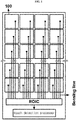
- FIG. 1 is a view illustrating a conventional touch panel.
- sensing lines are connected to touch electrodes, respectively. Accordingly, structure of the touch panel becomes complicated and manufacturing cost of the touch panel is high.
- the invention provides a touch panel where touch/fingerprint recognition electrodes disposed in a row share one sensing line. Additionally, the invention provides a touch panel capable of driving selectively touch point detection and fingerprint recognition and a readout method in the same.
- a self capacitive touch panel comprising: (m ⁇ n) sub-pixels, m and n being positive integer, respectively; and a driver configured to drive the sub-pixels.
- touch/fingerprint recognition electrodes of sub-pixels in a row share one sensing line.
- a self capacitive touch panel comprising: pixels configured to have sub-pixels, respectively; and a driver configured to drive the pixels.
- touch/fingerprint recognition electrodes including the pixels in a row share one sensing line.
- a self capacitive touch panel comprising: pixel arrays configured to have pixels, respectively; and a driver configured to drive the pixels.
- each of the pixels has at least one sub-pixel, and touch/fingerprint recognition electrodes including pixel arrays in a row share one sensing line.
- a touch panel comprising: (m ⁇ n) sub-pixels, m and n being positive integer, respectively; and a driver configured to drive the sub-pixels.
- at least one of the sub-pixels has a display transistor, a liquid crystal, a storage capacitor and a switching transistor, one of the switching transistor is connected to a node between the liquid crystal and the storage capacitor, other terminal of the switching transistor is connected to a scan line, and the display transistor is connected to a gate driver and a data driver.
- a touch panel comprising: touch sensors; and a driver configured to drive the touch sensors.
- the touch sensors has sub-pixels, and touch electrodes including sub-pixels in a row share one sensing line.
- touch/fingerprint recognition electrodes disposed in a row share one sensing line, and thus a structure of the touch panel becomes simple and manufacturing cost of the touch panel may reduce.
- the touch panel and a readout method in the same according to the invention may drive selectively touch point detection and fingerprint recognition.
- the invention relates to a touch panel, touch/fingerprint recognition electrodes including sub-pixels, pixels or pixel arrays disposed in a row may share one sensing line.
- the touch panel may be a panel for performing both of touch point detection and fingerprint recognition or a panel for performing only the touch point detection.
- a technique of sharing the sensing line according to the invention is more proper to a self capacitive touch panel.
- a touch/fingerprint recognition electrode may be formed with small number of sub-pixels, e.g. 3 ⁇ 3 sub pixels in a touch panel for performing both of touch point detection and fingerprint recognition, but a touch electrode may be formed with many number of sub-pixels, e.g. 100 ⁇ 100 sub-pixels in a touch panel for performing only touch point detection without fingerprint recognition.
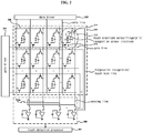
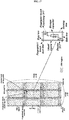
- FIG. 2 is a view illustrating circuit of a touch panel according to one embodiment of the invention
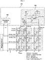
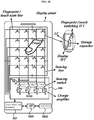
- FIG. 3 is a view illustrating circuit for touch detection method in the touch panel according to one embodiment of the invention
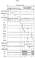
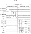
- FIG. 4 is a timing diagram illustrating signals used in the touch detection method of FIG. 3
- FIG. 5 is a view illustrating circuit for a fingerprint recognition method in a touch panel according to another embodiment of the invention
- FIG. 6 is a timing diagram illustrating signals used in the fingerprint recognition method of FIG. 5
- FIG. 7 is a timing diagram illustrating signals used in the fingerprint recognition method in the touch panel according to another embodiment of the invention.
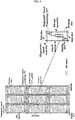
- FIG. 8 is a view illustrating layout of the touch panel of FIG. 2 using an IPS mode according to one embodiment of the invention
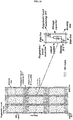
- FIG. 9 is a view illustrating layout of the touch panel of FIG. 2 using an FFS mode according to one embodiment of the invention
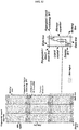
- FIG. 10 is a view illustrating layout of the touch panel of FIG. 2 using a VA mode according to one embodiment of the invention.
- the touch panel of the present embodiment may be for example liquid crystal display device, and perform both of touch point detection and fingerprint recognition.
- the touch panel may be a self capacitive touch panel.
- the touch panel may include a touch electrode 200, a data driver 202, a gate driver 204, a readout circuit ROIC 206 and a touch detection processor 207.
- the data driver 202 and the gate driver 204 may be included in a display driver.
- the touch electrode 200 includes at least one pixel 208, and the pixel 208 may include three sub-pixels 210 for recognizing fingerprint as shown in a dotted line box in FIG. 2 . On the other hand, the pixel 208 may include four sub-pixels not three sub-pixels.
- a fingerprint recognition electrode including one sub-pixel 210 may be referred to as a fingerprint recognition sensor in that it can recognize the fingerprint.
- a fingerprint recognition electrode including sub-pixels 210, i.e. one pixel 208 may be referred to as the fingerprint recognition sensor, or a fingerprint recognition electrode including a pixel array having pixels 208 may be referred to as the fingerprint recognition sensor.
- the fingerprint recognition electrode including one sub-pixel 210 is the fingerprint recognition sensor for convenience of description.
- the touch sensor includes m (positive integer) ⁇ n (positive integer) fingerprint recognition sensors.
- m means a number of sub-pixels in a row direction
- n indicates a number of sub-pixels in a horizontal direction.
- total number of the sub-pixels equals to M ⁇ N.
- the sub-pixel 210 includes a liquid crystal LC, a storage capacitor C, a display thin film transistor TFT 212 and a switching TFT 214 as shown in a circular dotted line of FIG. 2 .
- the LC, the C and the display TFT 212 are the same as in conventional liquid crystal display panel, and thus any further description concerning the elements will be omitted.
- a gate of the display TFT 212 is connected to a gate line, and a drain/a source of the display TFT 212 is connected to a data line.
- the sub-pixel 210 further includes the switching TFT 214 compared with conventional sub-pixel.
- a gate of the switching TFT 214 is connected to corresponding scan line, a drain/a source is connected to a node between the LC and the C, a source/a drain is connected to a sensing line.
- the scan line does not exist in the conventional touch panel, and crosses over the sensing line, preferably is vertically disposed to the sensing line.
- the readout circuit 206 may transmit signals for driving the touch/fingerprint recognition electrodes to the touch/fingerprint recognition electrodes through the scan lines, and sense self capacitance or mutual capacitance of the touch/fingerprint recognition electrodes through the sensing line.
- the touch panel of the present embodiment further includes the switching TFTs 214 and the scan lines which are connected to the switching TFTs 214 and provide signals to the switching TFTs 214.
- Touch/fingerprint recognition electrodes disposed in a row may share one sensing line as shown in FIG. 2 .
- the touch electrodes are connected to different sensing lines, respectively.
- the touch panel may selectively drive the touch point detection and the fingerprint recognition.
- the sensing lines are connected to charge amplifiers (circuit of lowest position in the readout circuit) via sensing switches.
- the sensing switches don't exist in the conventional technique.
- the readout circuit 206 transmits signals to the sub-pixels 210 through the scan lines, and senses self capacitance or mutual capacitance of corresponding touch sensor (particularly, touch/fingerprint recognition electrode) through the sensing lines.
- the signal may be a square wave, a sine wave, a saw tooth wave, a rectangular wave, etc.
- the touch detection processor 207 is connected to the readout circuit 206, and detects touch point or obtains fingerprint information through capacitance sensed by the readout circuit 206.
- the touch/fingerprint recognition electrodes of the sub-pixels disposed in a row share one sensing line.
- the touch panel may include further the switching TFT 214, the scan line and the sensing switch, for the purpose of sharing of the sensing line.
- This structure may be applied to a touch panel in an In-Plane Switching IPS mode, a touch panel in a Fringe-Field Switching FFS mode and a touch panel in a Vertical Alignment VA mode, respectively. Layouts of the touch panels according to the modes are shown in FIG. 8 to FIG. 10 .
- the scan line, the sensing line and the switching TFT 214 may be disposed in a black matrix BM area.
- the touch/fingerprint recognition electrodes may use a vertical field driven method such as a twisted nematic TN mode and the VA mode, or a horizontal field driven method such as the IPS mode and the FFS mode.
- SCAN_D means a signal of a gate line
- SCAN_F indicates a signal of a scan line
- DATA means a signal of a data line
- Tdisplay indicates a display TFT
- Ttouch means a switching TFT
- SS indicates a sensing switch.
- the readout circuit 206 provides a VCOM volage to a common electrode through the sensing lines.
- the readout circuit 206 transmits signals to the sub-pixels 210 through every scan line.
- the readout circuit 206 turns on simultaneously the sensing switches between the scan lines and charge amplifiers.
- the readout circuit 206 senses self capacitance or mutual capacitance of the touch electrodes through the sensing lines, and the touch detection processor 207 detects touch point through the sensed capacitance.
- SCAN_D means a signal of the gate line
- SCAN_F indicates a signal of the scan line
- DATA means a signal of the data line
- Tdisplay indicates the display TFT
- Ttouch means the switching TFT
- SS indicates the sensing switch.
- the readout circuit 206 provides a VCOM voltage to the common electrode through the sensing lines.
- an excitation circuit 302 of the readout circuit 206 transmits a signal to one of the scan lines as shown in FIG. 6 , but does not provide a signal to the other scan lines.
- the sensing switches SS between the sensing lines and the charge amplifiers are sequentially connected during a high logic interval of the signal transmitted to the scan line. That is, the sensing lines are sequentially activated.
- a sensing circuit 300 of the readout circuit 206 senses self capacitance or mutual capacitance of fingerprint recognition electrodes connected to the sensing lines.
- the above process may be repeatedly performed for each of the scan lines to which signals are transmitted in sequence. Detailed operation for the scan lines is shown in FIG. 6 .
- the sensing circuit 300 of the readout circuit 206 may sense self capacitance or mutual capacitance of the fingerprint recognition electrodes, and the touch detection processor 207 may obtain fingerprint information through the sensed self capacitance or mutual capacitance.
- Orthogonal signals are simultaneously transmitted to every scan line as shown in FIG. 7 .
- the sensing switches SS between the sensing lines and the charge amplifiers are simultaneously connected.
- the readout circuit 206 may sense self capacitance or mutual capacitance of the fingerprint recognition electrodes at a sub-pixel connected to the scan lines to which the signals are transmitted, and the touch detection processor 207 may obtain fingerprint information through the sensed self capacitance or mutual capacitance.
- FIG. 11 is a view illustrating circuit of a touch panel according to another embodiment of the invention
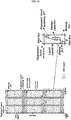
- FIG. 12 is a view illustrating layout of the touch panel in FIG. 11 using an IPS mode according to one embodiment of the invention
- FIG. 13 is a view illustrating layout of the touch panel in FIG. 11 according to an FFS mode
- FIG. 14 is a view illustrating layout of the touch panel in FIG. 11 according to one embodiment of the invention.
- FIG. 15 is a view illustrating layout of the touch panel using the IPS mode according to another embodiment of the invention
- FIG. 16 is a view illustrating layout of the touch panel using the FFS mode according to still another embodiment of the invention
- FIG. 17 is a view illustrating layout of the touch panel using the VA mode according to still another embodiment of the invention.
- the touch panel of the present embodiment may include touch electrodes 1100, a data driver 1102, a gate driver 1104, a readout circuit 1106 and a touch detection processor (not shown).
- the pixel 1108 may include three sub-pixels 1110.
- only one of the sub-pixels 1110 in the pixel 1108 may include the switching TFT.
- only rightmost sub-pixel includes a switching TFT.
- a sub-pixel including the switching TFT may be any sub-pixel as long as only one of the sub-pixels 1110 in the pixel 1108 includes the switching TFT.
- the touch/fingerprint recognition electrodes of the pixels 1108 disposed in a row may share one sensing line.
- touch/fingerprint recognition electrodes of sub-pixels in the same row of the pixels 1108 may share one sensing line.
- This structure may be applied to the touch panel in the IPS mode, the touch panel in the FFS mode and the touch panel in the VA mode. Layouts of the touch panels are shown in FIG. 12 to FIG 14 .
- the scan line, the sensing line and the switching TFT may be disposed in the black matrix BM area.
- the touch/fingerprint recognition electrodes may use the vertical field driven method such as the TN mode and the VA mode or the horizontal field driven method such as the IPS mode and the FFS mode.
- the touch/fingerprint recognition electrodes of the pixels 1108 disposed in a row share one sensing line, and thus the touch panel may detect the touch point and obtain the fingerprint information.
- An operation of the touch panel is similar to that in FIG. 2 , which is not described above.
- touch/fingerprint recognition electrodes in a unit of a pixel array not in a unit of a sub-pixel or a pixel may share one sensing line. That is, the touch/fingerprint recognition electrodes of pixel arrays disposed in the same row may share one sensing line.
- the touch/fingerprint recognition electrode of the pixel array connected to the sensing line is connected to the switching TFT, and the switching TFT is connected to the scan line.
- This structure may be applied to the touch panel in the IPS mode, the touch panel in the FFS mode and the touch panel in the VA mode. Layouts of the touch panels are shown in FIG. 15 to FIG. 17 .
- the scan line, the sensing line and the switching TFT may be disposed in the black matrix BM area.
- the touch/fingerprint recognition electrodes may use the vertical field driven method such as the TN mode and the VA mode or the horizontal field driven method such as the IPS mode and the FFS mode.
- FIG. 18 is a view illustrating a computing device using a touch panel according to one embodiment of the invention
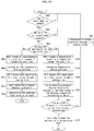
- FIG. 19 is a flowchart illustrating an operation of the computing device in FIG. 18 according to one embodiment of the invention.
- the computing device of the present embodiment may further include an application processor AP 1800 and a controller 1802 other than elements in FIG. 2 .
- the application processor 1800 executes an application (program for internet banking, mobile payment, electronic document exchanging, etc.), and it is necessary to certify a user before driving the application in an operation mode. Accordingly, a fingerprint recognition process should be performed so as to certify the user.
- the application processor 1800 may verify whether user's fingerprint information is identical to the obtained fingerprint information, for the purpose of user's certification. Of course, the user's fingerprint information is stored in advance.
- a self-certification verifying window may be displayed on a display screen when the fingerprint recognition process is performed.
- the controller 1802 may change the application in the operation mode when the user's fingerprint information is identical to the obtained fingerprint information, i.e. the user is certified.
- a switch S1 of the sensing circuit 300 in the readout circuit 206 is off state, when the touch input by the user is sensed.
- step of S1904 it is discriminated that the application processor AP 1800 executes the application for user certification, when the switch S1 is off state, i.e. in touch phase.
- the readout circuit 206 transmits simultaneously signals to m scan lines, when the application for the user certification is not executed.
- the readout circuit 206 turns on n sensing switches.
- the readout circuit 206 senses for example self capacitance or mutual capacitance of the touch electrode through n sensing lines.
- the touch point processor 207 detects the touch point through the sensed capacitance.
- the controller 1802 determines the detected touch point as an input.
- the readout circuit 206 transmits sequentially signals to the scan lines when the application for user certification is executed.
- the readout circuit 206 turns on sequentially the sensing switches so as to recognize the fingerprint.
- the readout circuit 206 senses self capacitance or mutual capacitance of the fingerprint recognition electrodes through the sensing lines.
- the touch detection processor 207 obtains fingerprint information through the sensed capacitance, and transmits the obtained fingerprint information to the application processor 1800.
- the application processor 1800 discriminates that the obtained fingerprint information is identical to user information.
- an access impossible message is displayed on the display screen when the obtained fingerprint information is not identical to the user information.
- the controller 1802 changes the application in the operation mode when the obtained fingerprint information is identical to the user information.
- the touch panel performs both of the touch point detection and the fingerprint recognition in above description.
- a structure and an operation of a touch panel for performing only touch point detection without the fingerprint recognition will be described in detail.
- FIG. 20 is a view illustrating a touch panel according to still another embodiment of the invention
- FIG. 21 is a view illustrating circuit for touch detection method in the touch panel in FIG. 20 according to one embodiment of the invention
- FIG. 22 is a timing diagram illustrating signals used in the touch detection method in FIG. 21 .
- the touch panel of the present embodiment includes touch sensors 2010, a readout circuit ROIC 2002 and a touch detection processor 2004.
- the touch sensor 2010 forms a touch electrode with sub-pixels as shown in a circular dotted line.
- touch electrodes disposed in the same row share one sensing line.
- Each of the touch sensors 2010 includes one switching TFT 2020 connected to the sensing line, and corresponding scan line is connected to a gate of the switching TFT 2020.
- the readout circuit 2002 includes a sensing circuit 2110 and an excitation circuit 2112.
- the readout circuit 2002 may not include a sensing switch unlike in FIG. 2 .
- the excitation circuit 2112 transmits signals to the switching TFTs 2020 through the scan lines.
- the sensing circuit 2110 senses self capacitance or mutual capacitance of the touch electrode 2010 through the sensing line.
- the touch detection processor 2004 detects touch point through the sensed capacitance.
- the readout circuit 2002 transmits sequentially signals to the scan lines.
- the readout circuit 2002 senses sequentially self capacitance or mutual capacitance of a touch electrode corresponding to the scan line to which the signal is transmitted.
- the touch detection processor 2004 detects touch point through the sensed capacitance.
- the readout circuit 2002 transmits simultaneously orthogonal signals to the scan lines, and then senses simultaneously self capacitance or mutual capacitance of every touch electrode.
- the touch detection circuit 2002 detects touch point through the sensed capacitance.
- the touch electrodes disposed in a row in the touch panel of the present embodiment share one sensing line.
- FIG. 23 is a view illustrating a computing device according to another embodiment of the invention
- FIG. 24 is a flowchart illustrating a touch recognition process in the touch panel in FIG. 23 according to one embodiment of the invention.
- a switch S1 of the sensing circuit 2110 in the readout circuit 2002 is off state, i.e. in touch phase.
- step of S2402 user's touch input is sensed when the switch S1 is off state.
- the readout circuit 2002 transmits signals to the scan lines when the user's touch input is sensed.
- the readout circuit 2002 senses self capacitance or mutual capacitance of the touch electrodes through the sensing lines.
- the touch detection processor 2004 detects touch point through the sensed capacitance.
- the application processor 2300 or the controller 2302 determines the detected touch point as an input.
- a computer-readable medium can include program instructions, data files, data structures, etc., alone or in combination.
- the program instructions recorded on the medium can be designed and configured specifically for the present invention or can be a type of medium known to and used by the skilled person in the field of computer software.
- Examples of a computer-readable medium may include magnetic media such as hard disks, floppy disks, magnetic tapes, etc., optical media such as CD-ROM's, DVD's, etc., magneto-optical media such as floptical disks, etc., and hardware devices such as ROM, RAM, flash memory, etc.
- Examples of the program of instructions may include not only machine language codes produced by a compiler but also high-level language codes that can be executed by a computer through the use of an interpreter, etc.
- the hardware mentioned above can be made to operate as one or more software modules that perform the actions of the embodiments of the invention, and vice versa.
Landscapes
- Engineering & Computer Science (AREA)
- Theoretical Computer Science (AREA)
- General Engineering & Computer Science (AREA)
- Human Computer Interaction (AREA)
- Physics & Mathematics (AREA)
- General Physics & Mathematics (AREA)
- Multimedia (AREA)
- Image Input (AREA)
- Position Input By Displaying (AREA)
- Measurement Of Length, Angles, Or The Like Using Electric Or Magnetic Means (AREA)
- Liquid Crystal (AREA)
Abstract
Description
- This application claims priority under 35 U.S.C. § 119(a) to a Korean patent application filed on August 26, 2016 in the Korean Intellectual Property Office and assigned Serial No.
10-2016-0108869 PCT/KR2017/007235 filed on July 6, 2017 - The present disclosure relates to a touch panel where touch/fingerprint recognition electrodes disposed in a row share one sensing line. Touch point detection and fingerprint recognition may be selectively driven through the touch panel and a readout method of the present disclosure.
- A touch panel, e.g. a touch panel used in a liquid crystal display device is used for detecting touch point.
-
FIG. 1 is a view illustrating a conventional touch panel. - As shown in
FIG. 1 , in the conventional touch panel, sensing lines are connected to touch electrodes, respectively. Accordingly, structure of the touch panel becomes complicated and manufacturing cost of the touch panel is high. - The invention provides a touch panel where touch/fingerprint recognition electrodes disposed in a row share one sensing line. Additionally, the invention provides a touch panel capable of driving selectively touch point detection and fingerprint recognition and a readout method in the same.
- According to one embodiment of the invention, a self capacitive touch panel comprising: (m×n) sub-pixels, m and n being positive integer, respectively; and a driver configured to drive the sub-pixels. Here, touch/fingerprint recognition electrodes of sub-pixels in a row share one sensing line.
- According to another embodiment of the invention, a self capacitive touch panel comprising: pixels configured to have sub-pixels, respectively; and a driver configured to drive the pixels. Here, touch/fingerprint recognition electrodes including the pixels in a row share one sensing line.
- According to still another embodiment of the invention, a self capacitive touch panel comprising: pixel arrays configured to have pixels, respectively; and a driver configured to drive the pixels. Here, each of the pixels has at least one sub-pixel, and touch/fingerprint recognition electrodes including pixel arrays in a row share one sensing line.
- According to still another embodiment of the invention, a touch panel comprising: (m×n) sub-pixels, m and n being positive integer, respectively; and a driver configured to drive the sub-pixels. Here, at least one of the sub-pixels has a display transistor, a liquid crystal, a storage capacitor and a switching transistor, one of the switching transistor is connected to a node between the liquid crystal and the storage capacitor, other terminal of the switching transistor is connected to a scan line, and the display transistor is connected to a gate driver and a data driver.
- According to still another embodiment of the invention, a touch panel comprising: touch sensors; and a driver configured to drive the touch sensors. Here, at least one of the touch sensors has sub-pixels, and touch electrodes including sub-pixels in a row share one sensing line.
- In a touch panel of the invention, touch/fingerprint recognition electrodes disposed in a row share one sensing line, and thus a structure of the touch panel becomes simple and manufacturing cost of the touch panel may reduce. Moreover, the touch panel and a readout method in the same according to the invention may drive selectively touch point detection and fingerprint recognition.
- The aspects, features, advantages and embodiments of the invention will be more apparent from the following detailed description taken in conjunction with reference to the accompanying drawings, in which:
-
FIG. 1 is a view illustrating a conventional touch panel; -
FIG. 2 is a view illustrating circuit of a touch panel according to one embodiment of the invention; -
FIG. 3 is a view illustrating circuit for touch detection method in the touch panel according to one embodiment of the invention; -
FIG. 4 is a timing diagram illustrating signals used in the touch detection method ofFIG. 3 ; -
FIG. 5 is a view illustrating circuit for a fingerprint recognition method in a touch panel according to another embodiment of the invention; -
FIG. 6 is a timing diagram illustrating signals used in the fingerprint recognition method ofFIG. 5 ; -
FIG. 7 is a timing diagram illustrating signals used in the fingerprint recognition method in the touch panel according to another embodiment of the invention; -
FIG. 8 is a view illustrating layout of the touch panel ofFIG. 2 using an IPS mode according to one embodiment of the invention; -
FIG. 9 is a view illustrating layout of the touch panel ofFIG. 2 using an FFS mode according to one embodiment of the invention; -
FIG. 10 is a view illustrating layout of the touch panel ofFIG. 2 using a VA mode according to one embodiment of the invention; -
FIG. 11 is a view illustrating circuit of a touch panel according to another embodiment of the invention; -
FIG. 12 is a view illustrating layout of the touch panel inFIG. 11 using an IPS mode according to one embodiment of the invention; -
FIG. 13 is a view illustrating layout of the touch panel inFIG. 11 according to an FFS mode; -
FIG. 14 is a view illustrating layout of the touch panel inFIG. 11 according to one embodiment of the invention; -
FIG. 15 is a view illustrating layout of the touch panel using the IPS mode according to another embodiment of the invention; -
FIG. 16 is a view illustrating layout of the touch panel using the FFS mode according to still another embodiment of the invention; -
FIG. 17 is a view illustrating layout of the touch panel using the VA mode according to still another embodiment of the invention; -
FIG. 18 is a view illustrating a computing device using a touch panel according to one embodiment of the invention; -
FIG. 19 is a flowchart illustrating an operation of the computing device inFIG. 18 according to one embodiment of the invention; -
FIG. 20 is a view illustrating a touch panel according to still another embodiment of the invention; -
FIG. 21 is a view illustrating circuit for touch detection method in the touch panel inFIG. 20 according to one embodiment of the invention; -
FIG. 22 is a timing diagram illustrating signals used in the touch detection method inFIG. 21 ; -
FIG. 23 is a view illustrating a computing device according to another embodiment of the invention; and -
FIG. 24 is a flowchart illustrating a touch recognition process in the touch panel inFIG. 23 according to one embodiment of the invention. - In the present specification, an expression used in the singular encompasses the expression of the plural, unless it has a clearly different meaning in the context. In the present specification, terms such as "comprising" or "including," etc., should not be interpreted as meaning that all of the elements or operations are necessarily included. That is, some of the elements or operations may not be included, while other additional elements or operations may be further included. Also, terms such as "unit," "module," etc., as used in the present specification may refer to a part for processing at least one function or action and may be implemented as hardware, software, or a combination of hardware and software.
- The invention relates to a touch panel, touch/fingerprint recognition electrodes including sub-pixels, pixels or pixel arrays disposed in a row may share one sensing line. Here, the touch panel may be a panel for performing both of touch point detection and fingerprint recognition or a panel for performing only the touch point detection.
- Specially, a technique of sharing the sensing line according to the invention is more proper to a self capacitive touch panel.
- A touch/fingerprint recognition electrode may be formed with small number of sub-pixels, e.g. 3×3 sub pixels in a touch panel for performing both of touch point detection and fingerprint recognition, but a touch electrode may be formed with many number of sub-pixels, e.g. 100×100 sub-pixels in a touch panel for performing only touch point detection without fingerprint recognition.
- Hereinafter, embodiments of the invention will be described in detail with reference to accompanying drawings.
-
FIG. 2 is a view illustrating circuit of a touch panel according to one embodiment of the invention,FIG. 3 is a view illustrating circuit for touch detection method in the touch panel according to one embodiment of the invention, andFIG. 4 is a timing diagram illustrating signals used in the touch detection method ofFIG. 3 .FIG. 5 is a view illustrating circuit for a fingerprint recognition method in a touch panel according to another embodiment of the invention,FIG. 6 is a timing diagram illustrating signals used in the fingerprint recognition method ofFIG. 5 , andFIG. 7 is a timing diagram illustrating signals used in the fingerprint recognition method in the touch panel according to another embodiment of the invention.FIG. 8 is a view illustrating layout of the touch panel ofFIG. 2 using an IPS mode according to one embodiment of the invention,FIG. 9 is a view illustrating layout of the touch panel ofFIG. 2 using an FFS mode according to one embodiment of the invention, andFIG. 10 is a view illustrating layout of the touch panel ofFIG. 2 using a VA mode according to one embodiment of the invention. - In
FIG. 2 , the touch panel of the present embodiment may be for example liquid crystal display device, and perform both of touch point detection and fingerprint recognition. - In one embodiment, the touch panel may be a self capacitive touch panel.
- The touch panel may include a
touch electrode 200, adata driver 202, agate driver 204, areadout circuit ROIC 206 and atouch detection processor 207. On the other hand, thedata driver 202 and thegate driver 204 may be included in a display driver. - The
touch electrode 200 includes at least onepixel 208, and thepixel 208 may include threesub-pixels 210 for recognizing fingerprint as shown in a dotted line box inFIG. 2 . On the other hand, thepixel 208 may include four sub-pixels not three sub-pixels. - In view of fingerprint recognition, a fingerprint recognition electrode including one
sub-pixel 210 may be referred to as a fingerprint recognition sensor in that it can recognize the fingerprint. A fingerprint recognition electrode including sub-pixels 210, i.e. onepixel 208 may be referred to as the fingerprint recognition sensor, or a fingerprint recognition electrode including a pixelarray having pixels 208 may be referred to as the fingerprint recognition sensor. - Hereinafter, it is assumed that the fingerprint recognition electrode including one
sub-pixel 210 is the fingerprint recognition sensor for convenience of description. - In this case, the touch sensor includes m (positive integer)×n (positive integer) fingerprint recognition sensors. Here, m means a number of sub-pixels in a row direction, and n indicates a number of sub-pixels in a horizontal direction. On the other hand, it is assumed that total number of the sub-pixels equals to M× N.
- The sub-pixel 210 includes a liquid crystal LC, a storage capacitor C, a display thin
film transistor TFT 212 and a switchingTFT 214 as shown in a circular dotted line ofFIG. 2 . - The LC, the C and the
display TFT 212 are the same as in conventional liquid crystal display panel, and thus any further description concerning the elements will be omitted. A gate of thedisplay TFT 212 is connected to a gate line, and a drain/a source of thedisplay TFT 212 is connected to a data line. - In one embodiment, the sub-pixel 210 further includes the switching
TFT 214 compared with conventional sub-pixel. - A gate of the switching
TFT 214 is connected to corresponding scan line, a drain/a source is connected to a node between the LC and the C, a source/a drain is connected to a sensing line. Here, the scan line does not exist in the conventional touch panel, and crosses over the sensing line, preferably is vertically disposed to the sensing line. As a result, thereadout circuit 206 may transmit signals for driving the touch/fingerprint recognition electrodes to the touch/fingerprint recognition electrodes through the scan lines, and sense self capacitance or mutual capacitance of the touch/fingerprint recognition electrodes through the sensing line. - In view of the touch panel, the touch panel of the present embodiment further includes the switching
TFTs 214 and the scan lines which are connected to the switchingTFTs 214 and provide signals to the switchingTFTs 214. - Touch/fingerprint recognition electrodes disposed in a row may share one sensing line as shown in
FIG. 2 . In the conventional touch panel, specially self capacitive touch panel, the touch electrodes are connected to different sensing lines, respectively. The touch panel may selectively drive the touch point detection and the fingerprint recognition. - In one embodiment, the sensing lines are connected to charge amplifiers (circuit of lowest position in the readout circuit) via sensing switches. The sensing switches don't exist in the conventional technique.
- The
readout circuit 206 transmits signals to the sub-pixels 210 through the scan lines, and senses self capacitance or mutual capacitance of corresponding touch sensor (particularly, touch/fingerprint recognition electrode) through the sensing lines. Here, the signal may be a square wave, a sine wave, a saw tooth wave, a rectangular wave, etc. - The
touch detection processor 207 is connected to thereadout circuit 206, and detects touch point or obtains fingerprint information through capacitance sensed by thereadout circuit 206. - Briefly, in the touch panel of the present embodiment, the touch/fingerprint recognition electrodes of the sub-pixels disposed in a row share one sensing line. The touch panel may include further the switching
TFT 214, the scan line and the sensing switch, for the purpose of sharing of the sensing line. - This structure may be applied to a touch panel in an In-Plane Switching IPS mode, a touch panel in a Fringe-Field Switching FFS mode and a touch panel in a Vertical Alignment VA mode, respectively. Layouts of the touch panels according to the modes are shown in
FIG. 8 to FIG. 10 . - In one embodiment, the scan line, the sensing line and the switching
TFT 214 may be disposed in a black matrix BM area. - The touch/fingerprint recognition electrodes may use a vertical field driven method such as a twisted nematic TN mode and the VA mode, or a horizontal field driven method such as the IPS mode and the FFS mode.
- Hereinafter, a process of performing selectively the touch point detection and the fingerprint recognition by using circuits in
FIG. 2 to FIG. 6 will be described. - Firstly, a process of performing the touch point detection in the touch panel in
FIG. 2 will be described in detail with reference to drawingsFIG. 3 andFIG. 4 . InFIG. 3 andFIG. 4 , SCAN_D means a signal of a gate line, SCAN_F indicates a signal of a scan line, and DATA means a signal of a data line. Tdisplay indicates a display TFT, Ttouch means a switching TFT, and SS indicates a sensing switch. - In a display phase, the
readout circuit 206 provides a VCOM volage to a common electrode through the sensing lines. - Subsequently, in a touch/fingerprint phase, the
readout circuit 206 transmits signals to the sub-pixels 210 through every scan line. - Next, the
readout circuit 206 turns on simultaneously the sensing switches between the scan lines and charge amplifiers. - Subsequently, the
readout circuit 206 senses self capacitance or mutual capacitance of the touch electrodes through the sensing lines, and thetouch detection processor 207 detects touch point through the sensed capacitance. - Hereinafter, a process of performing the fingerprint recognition in the touch panel in
FIG. 2 will be described in detail with reference to drawingsFIG. 5 andFIG. 6 . InFIG. 5 andFIG. 6 , SCAN_D means a signal of the gate line, SCAN_F indicates a signal of the scan line, and DATA means a signal of the data line. Tdisplay indicates the display TFT, Ttouch means the switching TFT, and SS indicates the sensing switch. - In a display phase, the
readout circuit 206 provides a VCOM voltage to the common electrode through the sensing lines. - Subsequently, in a touch/fingerprint phase, an
excitation circuit 302 of thereadout circuit 206 transmits a signal to one of the scan lines as shown inFIG. 6 , but does not provide a signal to the other scan lines. - In this time, the sensing switches SS between the sensing lines and the charge amplifiers are sequentially connected during a high logic interval of the signal transmitted to the scan line. That is, the sensing lines are sequentially activated.
- A
sensing circuit 300 of thereadout circuit 206 senses self capacitance or mutual capacitance of fingerprint recognition electrodes connected to the sensing lines. - The above process may be repeatedly performed for each of the scan lines to which signals are transmitted in sequence. Detailed operation for the scan lines is shown in
FIG. 6 . - As a result, corresponding fingerprint recognition sensors operate sequentially for each of the scan lines. Here, the
sensing circuit 300 of thereadout circuit 206 may sense self capacitance or mutual capacitance of the fingerprint recognition electrodes, and thetouch detection processor 207 may obtain fingerprint information through the sensed self capacitance or mutual capacitance. - Hereinafter, a fingerprint recognition process according to another embodiment of the invention will be described in detail.
- Orthogonal signals are simultaneously transmitted to every scan line as shown in
FIG. 7 . - Subsequently, the sensing switches SS between the sensing lines and the charge amplifiers are simultaneously connected.
- As a result, the
readout circuit 206 may sense self capacitance or mutual capacitance of the fingerprint recognition electrodes at a sub-pixel connected to the scan lines to which the signals are transmitted, and thetouch detection processor 207 may obtain fingerprint information through the sensed self capacitance or mutual capacitance. -
FIG. 11 is a view illustrating circuit of a touch panel according to another embodiment of the invention,FIG. 12 is a view illustrating layout of the touch panel inFIG. 11 using an IPS mode according to one embodiment of the invention,FIG. 13 is a view illustrating layout of the touch panel inFIG. 11 according to an FFS mode, andFIG. 14 is a view illustrating layout of the touch panel inFIG. 11 according to one embodiment of the invention.FIG. 15 is a view illustrating layout of the touch panel using the IPS mode according to another embodiment of the invention,FIG. 16 is a view illustrating layout of the touch panel using the FFS mode according to still another embodiment of the invention, andFIG. 17 is a view illustrating layout of the touch panel using the VA mode according to still another embodiment of the invention. - In
FIG. 11 , the touch panel of the present embodiment may includetouch electrodes 1100, a data driver 1102, agate driver 1104, areadout circuit 1106 and a touch detection processor (not shown). - Since the other elements except a structure of a
pixel 1108 and related sensing line are the same as inFIG. 2 , any further description concerning the same elements will be omitted. - The
pixel 1108 may include three sub-pixels 1110. - In one embodiment, only one of the sub-pixels 1110 in the
pixel 1108 may include the switching TFT. In thepixel 1108 inFIG. 11 , only rightmost sub-pixel includes a switching TFT. Of course, a sub-pixel including the switching TFT may be any sub-pixel as long as only one of the sub-pixels 1110 in thepixel 1108 includes the switching TFT. - Only one of the sub-pixels 1110 in the
pixel 1108 includes the switching TFT inFIG. 11 , but two sub-pixels may include a switching TFT, respectively. That is, a number of the sub-pixel including the switching TFT is variously modified as long as every sub-pixel 1110 in thepixel 1108 does not include the switching TFT. - In one embodiment, the touch/fingerprint recognition electrodes of the
pixels 1108 disposed in a row may share one sensing line. Of course, touch/fingerprint recognition electrodes of sub-pixels in the same row of thepixels 1108 may share one sensing line. - This structure may be applied to the touch panel in the IPS mode, the touch panel in the FFS mode and the touch panel in the VA mode. Layouts of the touch panels are shown in
FIG. 12 to FIG 14 . - As shown in
FIG. 12 to FIG. 14 , the scan line, the sensing line and the switching TFT may be disposed in the black matrix BM area. - The touch/fingerprint recognition electrodes may use the vertical field driven method such as the TN mode and the VA mode or the horizontal field driven method such as the IPS mode and the FFS mode.
- Briefly, in the touch panel of the present embodiment, the touch/fingerprint recognition electrodes of the
pixels 1108 disposed in a row share one sensing line, and thus the touch panel may detect the touch point and obtain the fingerprint information. An operation of the touch panel is similar to that inFIG. 2 , which is not described above. - In another embodiment, touch/fingerprint recognition electrodes in a unit of a pixel array not in a unit of a sub-pixel or a pixel may share one sensing line. That is, the touch/fingerprint recognition electrodes of pixel arrays disposed in the same row may share one sensing line. Here, the touch/fingerprint recognition electrode of the pixel array connected to the sensing line is connected to the switching TFT, and the switching TFT is connected to the scan line.
- This structure may be applied to the touch panel in the IPS mode, the touch panel in the FFS mode and the touch panel in the VA mode. Layouts of the touch panels are shown in
FIG. 15 to FIG. 17 . - As shown in
FIG. 15 to FIG. 17 , the scan line, the sensing line and the switching TFT may be disposed in the black matrix BM area. - The touch/fingerprint recognition electrodes may use the vertical field driven method such as the TN mode and the VA mode or the horizontal field driven method such as the IPS mode and the FFS mode.
- Hereinafter, a structure and an operation of a computing device including the above touch panels will be described in detail with reference to accompanying drawings.
-
FIG. 18 is a view illustrating a computing device using a touch panel according to one embodiment of the invention, andFIG. 19 is a flowchart illustrating an operation of the computing device inFIG. 18 according to one embodiment of the invention. - In
FIG. 18 , the computing device of the present embodiment may further include anapplication processor AP 1800 and acontroller 1802 other than elements inFIG. 2 . - The
application processor 1800 executes an application (program for internet banking, mobile payment, electronic document exchanging, etc.), and it is necessary to certify a user before driving the application in an operation mode. Accordingly, a fingerprint recognition process should be performed so as to certify the user. Theapplication processor 1800 may verify whether user's fingerprint information is identical to the obtained fingerprint information, for the purpose of user's certification. Of course, the user's fingerprint information is stored in advance. - In one embodiment, a self-certification verifying window may be displayed on a display screen when the fingerprint recognition process is performed.
- The
controller 1802 may change the application in the operation mode when the user's fingerprint information is identical to the obtained fingerprint information, i.e. the user is certified. - Hereinafter, an operation of the computing device will be described in detail.
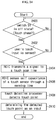
- In
FIG. 19 , in a step of S1900, it is discriminated whether or not touch input by the user is sensed. - In a step of S1902, it is discriminated that a switch S1 of the
sensing circuit 300 in thereadout circuit 206 is off state, when the touch input by the user is sensed. - In a step of S1904, it is discriminated that the
application processor AP 1800 executes the application for user certification, when the switch S1 is off state, i.e. in touch phase. - In a step of S1906, the
readout circuit 206 transmits simultaneously signals to m scan lines, when the application for the user certification is not executed. - In a step of S1908, the
readout circuit 206 turns on n sensing switches. - In a step of S1910, the
readout circuit 206 senses for example self capacitance or mutual capacitance of the touch electrode through n sensing lines. - In a step of S1912, the
touch point processor 207 detects the touch point through the sensed capacitance. - In a step of S1914, the
controller 1802 determines the detected touch point as an input. - In a step of S1916, the
readout circuit 206 transmits sequentially signals to the scan lines when the application for user certification is executed. - In a step of S1918, the
readout circuit 206 turns on sequentially the sensing switches so as to recognize the fingerprint. - In a step of S1920, the
readout circuit 206 senses self capacitance or mutual capacitance of the fingerprint recognition electrodes through the sensing lines. - In a step of S1922, the
touch detection processor 207 obtains fingerprint information through the sensed capacitance, and transmits the obtained fingerprint information to theapplication processor 1800. - In a step of S1924, the
application processor 1800 discriminates that the obtained fingerprint information is identical to user information. - In a step of S1926, an access impossible message is displayed on the display screen when the obtained fingerprint information is not identical to the user information.
- In a step of S1928, the
controller 1802 changes the application in the operation mode when the obtained fingerprint information is identical to the user information. - The touch panel performs both of the touch point detection and the fingerprint recognition in above description. Hereinafter, a structure and an operation of a touch panel for performing only touch point detection without the fingerprint recognition will be described in detail.
-
FIG. 20 is a view illustrating a touch panel according to still another embodiment of the invention,FIG. 21 is a view illustrating circuit for touch detection method in the touch panel inFIG. 20 according to one embodiment of the invention, andFIG. 22 is a timing diagram illustrating signals used in the touch detection method inFIG. 21 . - In
FIG. 20 andFIG. 21 , the touch panel of the present embodiment includestouch sensors 2010, areadout circuit ROIC 2002 and atouch detection processor 2004. - The
touch sensor 2010 forms a touch electrode with sub-pixels as shown in a circular dotted line. - In one embodiment, touch electrodes disposed in the same row share one sensing line.
- Each of the
touch sensors 2010 includes oneswitching TFT 2020 connected to the sensing line, and corresponding scan line is connected to a gate of the switchingTFT 2020. - The
readout circuit 2002 includes asensing circuit 2110 and anexcitation circuit 2112. Thereadout circuit 2002 may not include a sensing switch unlike inFIG. 2 . - The
excitation circuit 2112 transmits signals to the switchingTFTs 2020 through the scan lines. - The
sensing circuit 2110 senses self capacitance or mutual capacitance of thetouch electrode 2010 through the sensing line. - The
touch detection processor 2004 detects touch point through the sensed capacitance. - In
FIG. 21 andFIG. 22 , thereadout circuit 2002 transmits sequentially signals to the scan lines. - Subsequently, the
readout circuit 2002 senses sequentially self capacitance or mutual capacitance of a touch electrode corresponding to the scan line to which the signal is transmitted. - Next, the
touch detection processor 2004 detects touch point through the sensed capacitance. - In another embodiment, the
readout circuit 2002 transmits simultaneously orthogonal signals to the scan lines, and then senses simultaneously self capacitance or mutual capacitance of every touch electrode. - Subsequently, the
touch detection circuit 2002 detects touch point through the sensed capacitance. - Shortly, the touch electrodes disposed in a row in the touch panel of the present embodiment share one sensing line.
- Hereinafter, an operation of the touch panel in the computing device will be described in detail.
-
FIG. 23 is a view illustrating a computing device according to another embodiment of the invention, andFIG. 24 is a flowchart illustrating a touch recognition process in the touch panel inFIG. 23 according to one embodiment of the invention. - In
FIG. 23 andFIG. 24 , in a step of S2400, it is discriminated that a switch S1 of thesensing circuit 2110 in thereadout circuit 2002 is off state, i.e. in touch phase. - In a step of S2402, user's touch input is sensed when the switch S1 is off state.
- In a step of S2404, the
readout circuit 2002 transmits signals to the scan lines when the user's touch input is sensed. - In a step of S2406, the
readout circuit 2002 senses self capacitance or mutual capacitance of the touch electrodes through the sensing lines. - In a step of S2408, the
touch detection processor 2004 detects touch point through the sensed capacitance. - In a step of S2410, the
application processor 2300 or thecontroller 2302 determines the detected touch point as an input. - Components in the embodiments described above can be easily understood from the perspective of processes. That is, each component can also be understood as an individual process. Likewise, processes in the embodiments described above can be easily understood from the perspective of components.
- Also, the technical features described above can be implemented in the form of program instructions that may be performed using various computer means and can be recorded in a computer-readable medium. Such a computer-readable medium can include program instructions, data files, data structures, etc., alone or in combination. The program instructions recorded on the medium can be designed and configured specifically for the present invention or can be a type of medium known to and used by the skilled person in the field of computer software. Examples of a computer-readable medium may include magnetic media such as hard disks, floppy disks, magnetic tapes, etc., optical media such as CD-ROM's, DVD's, etc., magneto-optical media such as floptical disks, etc., and hardware devices such as ROM, RAM, flash memory, etc. Examples of the program of instructions may include not only machine language codes produced by a compiler but also high-level language codes that can be executed by a computer through the use of an interpreter, etc. The hardware mentioned above can be made to operate as one or more software modules that perform the actions of the embodiments of the invention, and vice versa.
- The embodiments of the invention described above are disclosed only for illustrative purposes. A person having ordinary skill in the art would be able to make various modifications, alterations, and additions without departing from the spirit and scope of the invention, but it is to be appreciated that such modifications, alterations, and additions are encompassed by the scope of claims set forth below.
Claims (22)
- A self capacitive touch panel comprising:(m×n) sub-pixels, m and n being positive integer, respectively; anda driver configured to drive the sub-pixels,wherein touch/fingerprint recognition electrodes including sub-pixels in a row share one sensing line.
- The self capacitive touch panel of claim 1, wherein the touch/fingerprint recognition electrode of the sub-pixel is a fingerprint recognition sensor capable of recognizing fingerprint, and the touch panel detects touch point and obtains fingerprint information through fingerprint recognition.
- The self capacitive touch panel of claim 1, wherein at least one of sub-pixels for sharing the sensing line includes a switching transistor which is turned on in a fingerprint recognition process,
and wherein one terminal of the switching transistor is connected to a node between a liquid crystal and a storage capacitor in corresponding sub-pixel, other terminal of the switching transistor is connected to a scan line, and the scan line and the sensing line are vertically disposed. - The self capacitive touch panel of claim 3, wherein the switching transistor, the scan line and the sensing line are disposed in a black matrix BM area.
- The self capacitive touch panel of claim 1, further comprising:a readout circuit configured to sense self capacitance of the touch/fingerprint recognition electrodes through the sensing line; anda touch detection processor configured to detect touch point or obtain fingerprint information through the sensed self capacitance,wherein the readout circuit further includes a sensing switch for transmitting a signal to the sub-pixel through a scan line connected to corresponding sub-pixel and switching connection between the scan line and a charge amplifier.
- The self capacitive touch panel of claim 5, wherein the touch/fingerprint recognition electrodes are connected to the readout circuit through scan lines and sensing lines are connected to the readout circuit,
and wherein in touch point detection, the readout circuit transmits simultaneously signals to the scan lines, turns on simultaneously sensing switches between the sensing lines and corresponding charge amplifiers and then senses self capacitance of the touch/fingerprint recognition electrodes through the sensing lines, and the touch detection processor detects the touch point through the sensed self capacitance. - The self capacitive touch panel of claim 5, wherein the touch/fingerprint recognition electrodes are connected to the readout circuit through scan lines and sensing lines are connected to the readout circuit,
and wherein when the fingerprint information is obtained, the readout circuit transmits a signal to corresponding touch/fingerprint recognition electrodes through a specific scan line, turns on sequentially sensing switches between the sensing line and corresponding charge amplifiers during a high logic interval of the signal and then senses self capacitance of the touch/fingerprint recognition electrodes through the sensing lines, and the touch detection processor obtains the fingerprint information through the sensed self capacitance. - The self capacitive touch panel of claim 5, wherein the touch/fingerprint recognition electrodes are connected to the readout circuit through scan lines and sensing lines are connected to the readout circuit,
and wherein when the fingerprint information is obtained, the readout circuit transmits simultaneously orthogonal signals to the scan lines, turns on simultaneously sensing switches between the sensing lines and corresponding charge amplifiers and then senses self capacitance of the touch/fingerprint recognition electrodes through the sensing lines, and the touch detection processor obtains the fingerprint information through the sensed self capacitance. - The self capacitive touch panel of claim 5, further comprising:an application processor AP connected to the touch detection processor; anda controller connected to the application processor,wherein the application processor verifies for user certification whether user's fingerprint information is identical to the obtained fingerprint information, and the controller changes the application in an operation mode when the user's fingerprint information is identical to the obtained fingerprint information.
- A self capacitive touch panel comprising:pixels configured to have sub-pixels, respectively; anda driver configured to drive the pixels,wherein touch/fingerprint recognition electrodes including the pixels in a row share one sensing line.
- The self capacitive touch panel of claim 10, wherein only one of sub-pixels in the pixel is used for sharing the sensing line, the sub-pixel used for sharing the sensing line includes a switching transistor which is connected to a scan line disposed vertically to the sensing line and is turned on when fingerprint is recognized,
and wherein one terminal of the switching transistor is connected to a node between a liquid crystal and a storage capacitor included in the sub-pixel, and other terminal of the switching transistor is connected to corresponding scan line. - The self capacitive touch panel of claim 10, further comprising:a readout circuit configured to sense self capacitance or mutual capacitance of the touch/fingerprint recognition electrodes through the sensing line; anda touch detection processor configured to detect touch point or obtain fingerprint information through the sensed self capacitance or mutual capacitance,wherein the readout circuit further includes a sensing switch which transmits a signal to the sub-pixel through a scan line connected to corresponding sub-pixel and switches connection between the scan line and a charge amplifier.
- A self capacitive touch panel comprising:pixel arrays configured to have pixels, respectively; anda driver configured to drive the pixels,wherein each of the pixels have at least one sub-pixel, and touch/fingerprint recognition electrodes including pixel arrays in a row share one sensing line.
- The self capacitive touch panel of claim 13, wherein only one of sub-pixels in the pixel array is used for sharing the sensing line, a sub-pixel used for sharing the sensing line includes a switching transistor which is connected to a scan line vertically disposed to the sensing line and is turned on when fingerprint is recognized,
and wherein one terminal of the switching transistor is connected to a node between a liquid crystal and a storage capacitor included in the sub-pixel, and other terminal of the switching transistor is connected to corresponding scan line. - The self capacitive touch panel of claim 13, further comprising:a readout circuit configured to sense self capacitance or mutual capacitance of the touch/fingerprint recognition electrode through the sensing line; anda touch detection processor configured to detect touch point or obtain fingerprint information through the sensed self capacitance or mutual capacitance,wherein the readout circuit further includes a sensing switch which transmits a signal to the sub-pixel through a scan line connected to corresponding sub-pixel and switches connection between the scan line and a charge amplifier.
- A touch panel comprising:(m×n) sub-pixels, m and n being positive integer, respectively; anda driver configured to drive the sub-pixels,wherein at least one of the sub-pixels has a display transistor, a liquid crystal, a storage capacitor and a switching transistor, one of the switching transistor is connected to a node between the liquid crystal and the storage capacitor, other terminal of the switching transistor is connected to a scan line, and the display transistor is connected to a gate driver and a data driver.
- The touch panel of claim 16, wherein touch electrodes of sub-pixels in a row share one sensing line.
- A touch panel comprising:touch sensors; anda driver configured to drive the touch sensors,wherein at least one of the touch sensors have sub-pixels, and touch electrodes including sub-pixels in a row share one sensing line.
- The touch panel of claim 18, wherein the touch panel detects only touch point without recognizing fingerprint,
only one of sub-pixels in the touch sensor is used for sharing the sensing line, and a sub-pixel used for sharing the sensing line includes a switching transistor connected to a scan line vertically disposed to the sensing line,
and wherein one terminal of the switching transistor is connected to a node between a liquid crystal and a storage capacitor included in the sub-pixel, and other terminal of the switching transistor is connected to corresponding scan line. - The touch panel of claim 18, further comprising:a readout circuit configured to sense self capacitance or mutual capacitance of the touch electrode through the sensing line; anda touch detection processor configured to detect touch point through the sensed self capacitance or mutual capacitance,wherein the readout circuit transmits a signal to the sub-pixel through a scan line connected to corresponding sub-pixel.
- The touch panel of claim 20, when in touch point detection, the readout circuit transmits sequentially signals to the scan lines and then senses self capacitance or mutual capacitance of a touch electrode corresponding to a scan line to which the signal is transmitted, and the touch detection processor detects the touch point through the sensed self capacitance or mutual capacitance.
- The touch panel of claim 20, wherein when the touch point is detected, the readout circuit transmits simultaneously orthogonal signals to the scan lines and then senses self capacitance or mutual capacitance of the touch electrodes, and the touch detection processor detects the touch point through the sensed self capacitance or mutual capacitance.
Applications Claiming Priority (2)
| Application Number | Priority Date | Filing Date | Title |
|---|---|---|---|
| KR1020160108869A KR101770521B1 (en) | 2016-08-26 | 2016-08-26 | Capacitive in-cell touch panel structures and their readout methods |
| PCT/KR2017/007235 WO2018038389A1 (en) | 2016-08-26 | 2017-07-06 | Capacitive in-cell touch panel and readout method thereof |
Publications (3)
| Publication Number | Publication Date |
|---|---|
| EP3506063A1 true EP3506063A1 (en) | 2019-07-03 |
| EP3506063A4 EP3506063A4 (en) | 2020-09-09 |
| EP3506063B1 EP3506063B1 (en) | 2023-12-13 |
Family
ID=59924750
Family Applications (1)
| Application Number | Title | Priority Date | Filing Date |
|---|---|---|---|
| EP17843809.9A Active EP3506063B1 (en) | 2016-08-26 | 2017-07-06 | Capacitive in-cell touch panel |
Country Status (5)
| Country | Link |
|---|---|
| US (1) | US11048368B2 (en) |
| EP (1) | EP3506063B1 (en) |
| KR (1) | KR101770521B1 (en) |
| CN (1) | CN109643186B (en) |
| WO (1) | WO2018038389A1 (en) |
Families Citing this family (14)
| Publication number | Priority date | Publication date | Assignee | Title |
|---|---|---|---|---|
| KR102686294B1 (en) * | 2016-12-23 | 2024-07-22 | 삼성디스플레이 주식회사 | Steering wheel and vehicle control system including the same |
| CN107623020B (en) * | 2017-09-08 | 2024-08-23 | 京东方科技集团股份有限公司 | Display panel, manufacturing method and display device |
| KR102502541B1 (en) * | 2018-02-21 | 2023-02-22 | 삼성전자주식회사 | An electronic device sensing fingerprint using selected electroids among a purality of electroids of biomtric seneor and control method thereof |
| CN110647253B (en) * | 2018-06-27 | 2023-05-26 | 鸿富锦精密工业(深圳)有限公司 | Touch display panel and electronic device using the touch display panel |
| CN110232268B (en) * | 2019-05-31 | 2021-12-28 | 武汉华星光电技术有限公司 | Fingerprint identification method, electronic equipment and display panel |
| CN110705429A (en) * | 2019-09-26 | 2020-01-17 | 合肥京东方光电科技有限公司 | Fingerprint recognition substrate and driving method of display device |
| TWI720682B (en) * | 2019-11-08 | 2021-03-01 | 友達光電股份有限公司 | Pixel array substrate |
| TWI735184B (en) * | 2020-03-17 | 2021-08-01 | 友達光電股份有限公司 | Display driver circuit and display device having the same |
| US20230152916A1 (en) * | 2020-04-29 | 2023-05-18 | Egis Technology Inc. | Electronic device having fingerprint sensing function |
| CN114078260B (en) * | 2020-08-18 | 2025-08-05 | 群创光电股份有限公司 | Fingerprint recognition method using electronic device and electronic device thereof |
| US12056307B2 (en) * | 2020-12-22 | 2024-08-06 | Fingerprint Cards Anacatum Ip Ab | Fingerprint sensor with column read-out |
| CN112766111B (en) * | 2021-01-08 | 2022-09-13 | 厦门天马微电子有限公司 | Display panel, driving method thereof and display device |
| US11551472B1 (en) * | 2021-09-27 | 2023-01-10 | Novatek Microelectronics Corp. | Method of fingerprint recognition and related fingerprint sensing circuit |
| KR20230093835A (en) * | 2021-12-20 | 2023-06-27 | 엘지디스플레이 주식회사 | Transparent display device with touch sensor |
Family Cites Families (56)
| Publication number | Priority date | Publication date | Assignee | Title |
|---|---|---|---|---|
| JP2002216117A (en) | 2001-01-24 | 2002-08-02 | Sony Corp | Capacitance detection type fingerprint detection device |
| JP4487430B2 (en) | 2001-02-15 | 2010-06-23 | 日本電気株式会社 | Fingerprint image input device with display function |
| JP5042316B2 (en) * | 2007-11-12 | 2012-10-03 | 三菱電機株式会社 | Touch panel and display device including the same |
| US7688082B2 (en) * | 2008-02-20 | 2010-03-30 | Himax Technologies Limited | Capacitive fingerprint sensor and the panel thereof |
| KR101462149B1 (en) * | 2008-05-22 | 2014-12-04 | 삼성디스플레이 주식회사 | Touch sensor, liquid crystal display panel having the same and method of sensing the same |
| KR101264727B1 (en) | 2009-09-24 | 2013-05-15 | 엘지디스플레이 주식회사 | Liquid Crystal Display Device with an Embedded Touch Panel therein |
| US9633247B2 (en) * | 2012-03-01 | 2017-04-25 | Apple Inc. | Electronic device with shared near field communications and sensor structures |
| US20140292666A1 (en) * | 2013-03-26 | 2014-10-02 | Mobile Identity Management and Biometrics consortium | Method and Apparatuses of User Interaction Control with Touch Display Device Integrated with Fingerprint Imager |
| US20130287272A1 (en) * | 2012-04-29 | 2013-10-31 | Yang Lu | Methods and Apparatus of Integrating Fingerprint Imagers with Touch Panels and Displays |
| TWI478029B (en) * | 2012-05-23 | 2015-03-21 | Hung Ta Liu | Touch control method |
| US8618865B1 (en) * | 2012-11-02 | 2013-12-31 | Palo Alto Research Center Incorporated | Capacitive imaging device with active pixels |
| CN103176676B (en) * | 2013-02-28 | 2015-10-14 | 合肥京东方光电科技有限公司 | A kind of touch screen touch point positioning detecting circuit, touch-screen and display device |
| KR101376228B1 (en) * | 2013-07-17 | 2014-04-01 | 실리콘 디스플레이 (주) | Fingerprint sensor capable of sensing fingerprint by optical method and capacitive method |
| US20150109214A1 (en) * | 2013-10-22 | 2015-04-23 | Weidong Shi | Methods and Apparatuses of touch-fingerprinting Display |
| CN103714330B (en) * | 2014-01-06 | 2017-12-19 | 苏州迈瑞微电子有限公司 | Capacitive fingerprint sensor |
| CN104898314B (en) * | 2014-03-07 | 2018-01-05 | 敦泰电子有限公司 | Display device and its drive circuit and driving method, electronic equipment |
| EP3640842B1 (en) * | 2014-03-12 | 2025-02-12 | Idex Biometrics Asa | Fingerprint detecting apparatus |
| US9836165B2 (en) * | 2014-05-16 | 2017-12-05 | Apple Inc. | Integrated silicon-OLED display and touch sensor panel |
| KR102264808B1 (en) * | 2014-06-23 | 2021-06-14 | 삼성전자주식회사 | Method for processing fingerprint and electronic device thereof |
| CN104155785B (en) * | 2014-08-07 | 2016-10-05 | 京东方科技集团股份有限公司 | Array base palte and driving method, display device |
| FR3025623B1 (en) * | 2014-09-05 | 2017-12-15 | Fogale Nanotech | CONTROL INTERFACE DEVICE AND FINGERPRINT SENSOR |
| KR102330586B1 (en) * | 2014-09-17 | 2021-11-24 | 엘지디스플레이 주식회사 | Apparatus for sensing touch/fingerprint |
| JP6472196B2 (en) * | 2014-09-17 | 2019-02-20 | 株式会社ワコム | Sensor signal processing circuit and sensor signal processing method |
| CN104282265B (en) * | 2014-09-26 | 2017-02-01 | 京东方科技集团股份有限公司 | Pixel circuit, drive method thereof, an organic light-emitting display panel and display device |
| TWI559185B (en) * | 2014-10-03 | 2016-11-21 | 速博思股份有限公司 | Display device with fingerprint recognition and touch detection |
| CN106796468B (en) * | 2014-10-10 | 2019-10-15 | 夏普株式会社 | display device |
| US9891746B2 (en) | 2014-11-12 | 2018-02-13 | Crucialtec Co., Ltd. | Display apparatus capable of image scanning and driving method thereof |
| US9679182B2 (en) * | 2014-11-12 | 2017-06-13 | Crucialtec Co., Ltd. | Display apparatus capable of image scanning and driving method thereof |
| KR20160056760A (en) * | 2014-11-12 | 2016-05-20 | 크루셜텍 (주) | Flexible display apparatus able to image scan and driving method thereof |
| KR20160061163A (en) | 2014-11-21 | 2016-05-31 | 삼성전자주식회사 | Method for registration and certification fingerprint and electronic device implementing the same |
| US9734787B2 (en) * | 2014-12-31 | 2017-08-15 | Htc Corporation | Method for operating mobile electronic device, mobile electronic device, and computer readable medium using the same |
| CN104536638A (en) * | 2015-01-07 | 2015-04-22 | 小米科技有限责任公司 | Touch key and fingerprint identification implementation method and device and terminal equipment |
| WO2016114795A1 (en) * | 2015-01-16 | 2016-07-21 | Silead (Cayman) Inc. | System and method for capacitive sensing |
| KR102350727B1 (en) | 2015-01-29 | 2022-01-14 | 엘지디스플레이 주식회사 | Touch screen display device including fingerprint sensor |
| CN105989327A (en) * | 2015-02-02 | 2016-10-05 | 神盾股份有限公司 | fingerprint sensing device and sensing method thereof |
| US20160253538A1 (en) * | 2015-02-28 | 2016-09-01 | Yang Lu | Methods and Apparatus of Integrating Fingerprint Imagers with Touch Panels and Displays |
| WO2016205832A1 (en) * | 2015-06-18 | 2016-12-22 | Shenzhen Huiding Technology Co., Ltd. | Multifunction fingerprint sensor having optical sensing capability |
| CN104881195B (en) * | 2015-06-18 | 2018-03-27 | 京东方科技集团股份有限公司 | A kind of driving method of array base palte |
| CN104881196B (en) * | 2015-06-23 | 2018-04-20 | 京东方科技集团股份有限公司 | Substrate and display screen |
| US10325131B2 (en) * | 2015-06-30 | 2019-06-18 | Synaptics Incorporated | Active matrix capacitive fingerprint sensor for display integration based on charge sensing by a 2-TFT pixel architecture |
| US9946375B2 (en) * | 2015-06-30 | 2018-04-17 | Synaptics Incorporated | Active matrix capacitive fingerprint sensor with 2-TFT pixel architecture for display integration |
| SE1551049A1 (en) * | 2015-07-29 | 2017-01-30 | Fingerprint Cards Ab | Acquisition of a fingerprint image |
| CN105183252B (en) * | 2015-08-13 | 2016-11-02 | 京东方科技集团股份有限公司 | A kind of array base palte, touch display screen, display device, driving method |
| WO2017034425A1 (en) * | 2015-08-21 | 2017-03-02 | Motorola Solutions, Inc. | System and method for disambiguating touch interactions |
| CN105046243B (en) * | 2015-08-25 | 2019-12-20 | 业成光电(深圳)有限公司 | Display device |
| CN105044952B (en) * | 2015-08-27 | 2018-05-22 | 京东方科技集团股份有限公司 | A kind of optical sensor and its driving method |
| CN105139793A (en) * | 2015-08-28 | 2015-12-09 | 京东方科技集团股份有限公司 | Array substrate, driving method therefor, display panel, and display device |
| CN105224845A (en) * | 2015-09-01 | 2016-01-06 | 京东方科技集团股份有限公司 | Identity recognition device and manufacture method, personal identification method |
| KR102395991B1 (en) * | 2015-10-29 | 2022-05-10 | 삼성전자주식회사 | Electronic apparatus including a touch-fingerprint complex sensor |
| CN105224139A (en) * | 2015-10-30 | 2016-01-06 | 深圳市汇顶科技股份有限公司 | Touch device and method for fingerprint detection on the touch device |
| US9547788B1 (en) * | 2015-11-13 | 2017-01-17 | Cypress Semiconductor Corporation | Fingerprint sensor-compatible overlay |
| US9760758B2 (en) * | 2015-12-30 | 2017-09-12 | Synaptics Incorporated | Determining which hand is being used to operate a device using a fingerprint sensor |
| CN105678258B (en) * | 2016-01-05 | 2019-04-02 | 京东方科技集团股份有限公司 | A fingerprint identification device, a driving method thereof, a display panel and a display device |
| TWI621997B (en) * | 2016-02-04 | 2018-04-21 | 速博思股份有限公司 | High efficiency fingerprint identification device |
| US10353511B2 (en) * | 2016-08-19 | 2019-07-16 | Qualcomm Incorporated | Capacitance-to-voltage modulation circuit |
| US20180218191A1 (en) * | 2017-01-31 | 2018-08-02 | Synaptics Incorporated | Outside of active area finger-print sensor |
-
2016
- 2016-08-26 KR KR1020160108869A patent/KR101770521B1/en active Active
-
2017
- 2017-07-06 EP EP17843809.9A patent/EP3506063B1/en active Active
- 2017-07-06 CN CN201780051812.0A patent/CN109643186B/en active Active
- 2017-07-06 US US16/327,636 patent/US11048368B2/en active Active
- 2017-07-06 WO PCT/KR2017/007235 patent/WO2018038389A1/en not_active Ceased
Also Published As
| Publication number | Publication date |
|---|---|
| US20190227652A1 (en) | 2019-07-25 |
| EP3506063A4 (en) | 2020-09-09 |
| EP3506063B1 (en) | 2023-12-13 |
| KR101770521B1 (en) | 2017-09-05 |
| CN109643186B (en) | 2022-05-31 |
| WO2018038389A1 (en) | 2018-03-01 |
| CN109643186A (en) | 2019-04-16 |
| US11048368B2 (en) | 2021-06-29 |
Similar Documents
| Publication | Publication Date | Title |
|---|---|---|
| EP3506063B1 (en) | Capacitive in-cell touch panel | |
| US9946401B2 (en) | Display device with integrated touch screen and method for driving the same | |
| US9046954B2 (en) | Display device integrated with touch screen and method of driving the same | |
| US9329718B2 (en) | Display device with input system and method for driving the same | |
| US10372257B2 (en) | Liquid crystal display device having a common voltage compensator | |
| US9280231B2 (en) | Disabling display lines during input sensing periods | |
| US9772704B2 (en) | Display/touch temporal separation | |
| US20170177111A1 (en) | Array substrate, touch screen and display apparatus containing the same, and method for driving the same | |
| JP4957597B2 (en) | Sensing circuit, driving method thereof, display device, and electronic device | |
| US20140176455A1 (en) | Touch panel device and method of controlling a touch panel device | |
| US20140204049A1 (en) | Display apparatus with touch sensing function | |
| JP2014149816A (en) | Display device attached with touch detection function and electronic device | |
| CN104169849A (en) | Touch panel excitation using a drive signal having time-varying characteristics | |
| CN104882092B (en) | A kind of embedded touch display screen and its driving method, display device | |
| US20150185810A1 (en) | Touch screen device, touch screen display device using the same, and driving method thereof | |
| US20140340340A1 (en) | Visual interface system | |
| US20140015801A1 (en) | Photo sensor type touch panel | |
| US9400578B2 (en) | Touch panel, touch screen apparatus, and method of driving the touch panel | |
| US9837007B2 (en) | In-cell touch liquid crystal display apparatus | |
| KR101882617B1 (en) | Capacitive in-cell touch panel structures and their readout methods | |
| CN104699369B (en) | Display device and its driving method | |
| TWI564765B (en) | Displaying device and driving circuit thereof and driving method and electronic equipment | |
| JP2009003414A (en) | Display device and electronic device | |
| JP5475498B2 (en) | Display device with touch panel | |
| CN112462974B (en) | A driving method for a touch display device, a driving circuit and a touch display device |
Legal Events
| Date | Code | Title | Description |
|---|---|---|---|
| STAA | Information on the status of an ep patent application or granted ep patent |
Free format text: STATUS: THE INTERNATIONAL PUBLICATION HAS BEEN MADE |
|
| PUAI | Public reference made under article 153(3) epc to a published international application that has entered the european phase |
Free format text: ORIGINAL CODE: 0009012 |
|
| STAA | Information on the status of an ep patent application or granted ep patent |
Free format text: STATUS: REQUEST FOR EXAMINATION WAS MADE |
|
| 17P | Request for examination filed |
Effective date: 20190322 |
|
| AK | Designated contracting states |
Kind code of ref document: A1 Designated state(s): AL AT BE BG CH CY CZ DE DK EE ES FI FR GB GR HR HU IE IS IT LI LT LU LV MC MK MT NL NO PL PT RO RS SE SI SK SM TR |
|
| AX | Request for extension of the european patent |
Extension state: BA ME |
|
| DAV | Request for validation of the european patent (deleted) | ||
| DAX | Request for extension of the european patent (deleted) | ||
| A4 | Supplementary search report drawn up and despatched |
Effective date: 20200812 |
|
| RIC1 | Information provided on ipc code assigned before grant |
Ipc: G06F 3/044 20060101ALI20200806BHEP Ipc: G06F 3/041 20060101AFI20200806BHEP Ipc: G06K 9/00 20060101ALI20200806BHEP |
|
| STAA | Information on the status of an ep patent application or granted ep patent |
Free format text: STATUS: EXAMINATION IS IN PROGRESS |
|
| 17Q | First examination report despatched |
Effective date: 20220310 |
|
| GRAP | Despatch of communication of intention to grant a patent |
Free format text: ORIGINAL CODE: EPIDOSNIGR1 |
|
| STAA | Information on the status of an ep patent application or granted ep patent |
Free format text: STATUS: GRANT OF PATENT IS INTENDED |
|
| RIC1 | Information provided on ipc code assigned before grant |
Ipc: G06F 3/044 20060101ALI20230612BHEP Ipc: G06F 3/041 20060101AFI20230612BHEP |
|
| INTG | Intention to grant announced |
Effective date: 20230704 |
|
| GRAS | Grant fee paid |
Free format text: ORIGINAL CODE: EPIDOSNIGR3 |
|
| GRAA | (expected) grant |
Free format text: ORIGINAL CODE: 0009210 |
|
| STAA | Information on the status of an ep patent application or granted ep patent |
Free format text: STATUS: THE PATENT HAS BEEN GRANTED |
|
| AK | Designated contracting states |
Kind code of ref document: B1 Designated state(s): AL AT BE BG CH CY CZ DE DK EE ES FI FR GB GR HR HU IE IS IT LI LT LU LV MC MK MT NL NO PL PT RO RS SE SI SK SM TR |
|
| REG | Reference to a national code |
Ref country code: GB Ref legal event code: FG4D |
|
| REG | Reference to a national code |
Ref country code: CH Ref legal event code: EP |
|
| REG | Reference to a national code |
Ref country code: DE Ref legal event code: R096 Ref document number: 602017077539 Country of ref document: DE |
|
| REG | Reference to a national code |
Ref country code: IE Ref legal event code: FG4D |
|
| PG25 | Lapsed in a contracting state [announced via postgrant information from national office to epo] |
Ref country code: GR Free format text: LAPSE BECAUSE OF FAILURE TO SUBMIT A TRANSLATION OF THE DESCRIPTION OR TO PAY THE FEE WITHIN THE PRESCRIBED TIME-LIMIT Effective date: 20240314 |
|
| REG | Reference to a national code |
Ref country code: LT Ref legal event code: MG9D |
|
| PG25 | Lapsed in a contracting state [announced via postgrant information from national office to epo] |
Ref country code: LT Free format text: LAPSE BECAUSE OF FAILURE TO SUBMIT A TRANSLATION OF THE DESCRIPTION OR TO PAY THE FEE WITHIN THE PRESCRIBED TIME-LIMIT Effective date: 20231213 |
|
| REG | Reference to a national code |
Ref country code: NL Ref legal event code: MP Effective date: 20231213 |
|
| PG25 | Lapsed in a contracting state [announced via postgrant information from national office to epo] |
Ref country code: ES Free format text: LAPSE BECAUSE OF FAILURE TO SUBMIT A TRANSLATION OF THE DESCRIPTION OR TO PAY THE FEE WITHIN THE PRESCRIBED TIME-LIMIT Effective date: 20231213 |
|
| PG25 | Lapsed in a contracting state [announced via postgrant information from national office to epo] |
Ref country code: LT Free format text: LAPSE BECAUSE OF FAILURE TO SUBMIT A TRANSLATION OF THE DESCRIPTION OR TO PAY THE FEE WITHIN THE PRESCRIBED TIME-LIMIT Effective date: 20231213 Ref country code: GR Free format text: LAPSE BECAUSE OF FAILURE TO SUBMIT A TRANSLATION OF THE DESCRIPTION OR TO PAY THE FEE WITHIN THE PRESCRIBED TIME-LIMIT Effective date: 20240314 Ref country code: ES Free format text: LAPSE BECAUSE OF FAILURE TO SUBMIT A TRANSLATION OF THE DESCRIPTION OR TO PAY THE FEE WITHIN THE PRESCRIBED TIME-LIMIT Effective date: 20231213 Ref country code: BG Free format text: LAPSE BECAUSE OF FAILURE TO SUBMIT A TRANSLATION OF THE DESCRIPTION OR TO PAY THE FEE WITHIN THE PRESCRIBED TIME-LIMIT Effective date: 20240313 |
|
| REG | Reference to a national code |
Ref country code: AT Ref legal event code: MK05 Ref document number: 1641004 Country of ref document: AT Kind code of ref document: T Effective date: 20231213 |
|
| PG25 | Lapsed in a contracting state [announced via postgrant information from national office to epo] |
Ref country code: NL Free format text: LAPSE BECAUSE OF FAILURE TO SUBMIT A TRANSLATION OF THE DESCRIPTION OR TO PAY THE FEE WITHIN THE PRESCRIBED TIME-LIMIT Effective date: 20231213 |
|
| PG25 | Lapsed in a contracting state [announced via postgrant information from national office to epo] |
Ref country code: SE Free format text: LAPSE BECAUSE OF FAILURE TO SUBMIT A TRANSLATION OF THE DESCRIPTION OR TO PAY THE FEE WITHIN THE PRESCRIBED TIME-LIMIT Effective date: 20231213 Ref country code: RS Free format text: LAPSE BECAUSE OF FAILURE TO SUBMIT A TRANSLATION OF THE DESCRIPTION OR TO PAY THE FEE WITHIN THE PRESCRIBED TIME-LIMIT Effective date: 20231213 Ref country code: NO Free format text: LAPSE BECAUSE OF FAILURE TO SUBMIT A TRANSLATION OF THE DESCRIPTION OR TO PAY THE FEE WITHIN THE PRESCRIBED TIME-LIMIT Effective date: 20240313 Ref country code: NL Free format text: LAPSE BECAUSE OF FAILURE TO SUBMIT A TRANSLATION OF THE DESCRIPTION OR TO PAY THE FEE WITHIN THE PRESCRIBED TIME-LIMIT Effective date: 20231213 Ref country code: LV Free format text: LAPSE BECAUSE OF FAILURE TO SUBMIT A TRANSLATION OF THE DESCRIPTION OR TO PAY THE FEE WITHIN THE PRESCRIBED TIME-LIMIT Effective date: 20231213 Ref country code: HR Free format text: LAPSE BECAUSE OF FAILURE TO SUBMIT A TRANSLATION OF THE DESCRIPTION OR TO PAY THE FEE WITHIN THE PRESCRIBED TIME-LIMIT Effective date: 20231213 |
|
| PG25 | Lapsed in a contracting state [announced via postgrant information from national office to epo] |
Ref country code: IS Free format text: LAPSE BECAUSE OF FAILURE TO SUBMIT A TRANSLATION OF THE DESCRIPTION OR TO PAY THE FEE WITHIN THE PRESCRIBED TIME-LIMIT Effective date: 20240413 |
|
| PG25 | Lapsed in a contracting state [announced via postgrant information from national office to epo] |
Ref country code: AT Free format text: LAPSE BECAUSE OF FAILURE TO SUBMIT A TRANSLATION OF THE DESCRIPTION OR TO PAY THE FEE WITHIN THE PRESCRIBED TIME-LIMIT Effective date: 20231213 Ref country code: CZ Free format text: LAPSE BECAUSE OF FAILURE TO SUBMIT A TRANSLATION OF THE DESCRIPTION OR TO PAY THE FEE WITHIN THE PRESCRIBED TIME-LIMIT Effective date: 20231213 |
|
| PG25 | Lapsed in a contracting state [announced via postgrant information from national office to epo] |
Ref country code: SK Free format text: LAPSE BECAUSE OF FAILURE TO SUBMIT A TRANSLATION OF THE DESCRIPTION OR TO PAY THE FEE WITHIN THE PRESCRIBED TIME-LIMIT Effective date: 20231213 |
|
| PG25 | Lapsed in a contracting state [announced via postgrant information from national office to epo] |
Ref country code: SM Free format text: LAPSE BECAUSE OF FAILURE TO SUBMIT A TRANSLATION OF THE DESCRIPTION OR TO PAY THE FEE WITHIN THE PRESCRIBED TIME-LIMIT Effective date: 20231213 Ref country code: SK Free format text: LAPSE BECAUSE OF FAILURE TO SUBMIT A TRANSLATION OF THE DESCRIPTION OR TO PAY THE FEE WITHIN THE PRESCRIBED TIME-LIMIT Effective date: 20231213 Ref country code: RO Free format text: LAPSE BECAUSE OF FAILURE TO SUBMIT A TRANSLATION OF THE DESCRIPTION OR TO PAY THE FEE WITHIN THE PRESCRIBED TIME-LIMIT Effective date: 20231213 Ref country code: IT Free format text: LAPSE BECAUSE OF FAILURE TO SUBMIT A TRANSLATION OF THE DESCRIPTION OR TO PAY THE FEE WITHIN THE PRESCRIBED TIME-LIMIT Effective date: 20231213 Ref country code: IS Free format text: LAPSE BECAUSE OF FAILURE TO SUBMIT A TRANSLATION OF THE DESCRIPTION OR TO PAY THE FEE WITHIN THE PRESCRIBED TIME-LIMIT Effective date: 20240413 Ref country code: EE Free format text: LAPSE BECAUSE OF FAILURE TO SUBMIT A TRANSLATION OF THE DESCRIPTION OR TO PAY THE FEE WITHIN THE PRESCRIBED TIME-LIMIT Effective date: 20231213 Ref country code: CZ Free format text: LAPSE BECAUSE OF FAILURE TO SUBMIT A TRANSLATION OF THE DESCRIPTION OR TO PAY THE FEE WITHIN THE PRESCRIBED TIME-LIMIT Effective date: 20231213 Ref country code: AT Free format text: LAPSE BECAUSE OF FAILURE TO SUBMIT A TRANSLATION OF THE DESCRIPTION OR TO PAY THE FEE WITHIN THE PRESCRIBED TIME-LIMIT Effective date: 20231213 |
|
| PG25 | Lapsed in a contracting state [announced via postgrant information from national office to epo] |
Ref country code: PT Free format text: LAPSE BECAUSE OF FAILURE TO SUBMIT A TRANSLATION OF THE DESCRIPTION OR TO PAY THE FEE WITHIN THE PRESCRIBED TIME-LIMIT Effective date: 20240415 Ref country code: PL Free format text: LAPSE BECAUSE OF FAILURE TO SUBMIT A TRANSLATION OF THE DESCRIPTION OR TO PAY THE FEE WITHIN THE PRESCRIBED TIME-LIMIT Effective date: 20231213 |
|
| PG25 | Lapsed in a contracting state [announced via postgrant information from national office to epo] |
Ref country code: PT Free format text: LAPSE BECAUSE OF FAILURE TO SUBMIT A TRANSLATION OF THE DESCRIPTION OR TO PAY THE FEE WITHIN THE PRESCRIBED TIME-LIMIT Effective date: 20240415 Ref country code: PL Free format text: LAPSE BECAUSE OF FAILURE TO SUBMIT A TRANSLATION OF THE DESCRIPTION OR TO PAY THE FEE WITHIN THE PRESCRIBED TIME-LIMIT Effective date: 20231213 |
|
| REG | Reference to a national code |
Ref country code: DE Ref legal event code: R097 Ref document number: 602017077539 Country of ref document: DE |
|
| PG25 | Lapsed in a contracting state [announced via postgrant information from national office to epo] |
Ref country code: DK Free format text: LAPSE BECAUSE OF FAILURE TO SUBMIT A TRANSLATION OF THE DESCRIPTION OR TO PAY THE FEE WITHIN THE PRESCRIBED TIME-LIMIT Effective date: 20231213 |
|
| PLBE | No opposition filed within time limit |
Free format text: ORIGINAL CODE: 0009261 |
|
| STAA | Information on the status of an ep patent application or granted ep patent |
Free format text: STATUS: NO OPPOSITION FILED WITHIN TIME LIMIT |
|
| PG25 | Lapsed in a contracting state [announced via postgrant information from national office to epo] |
Ref country code: SI Free format text: LAPSE BECAUSE OF FAILURE TO SUBMIT A TRANSLATION OF THE DESCRIPTION OR TO PAY THE FEE WITHIN THE PRESCRIBED TIME-LIMIT Effective date: 20231213 |
|
| PG25 | Lapsed in a contracting state [announced via postgrant information from national office to epo] |
Ref country code: SI Free format text: LAPSE BECAUSE OF FAILURE TO SUBMIT A TRANSLATION OF THE DESCRIPTION OR TO PAY THE FEE WITHIN THE PRESCRIBED TIME-LIMIT Effective date: 20231213 Ref country code: DK Free format text: LAPSE BECAUSE OF FAILURE TO SUBMIT A TRANSLATION OF THE DESCRIPTION OR TO PAY THE FEE WITHIN THE PRESCRIBED TIME-LIMIT Effective date: 20231213 |
|
| 26N | No opposition filed |
Effective date: 20240916 |
|
| PG25 | Lapsed in a contracting state [announced via postgrant information from national office to epo] |
Ref country code: MC Free format text: LAPSE BECAUSE OF FAILURE TO SUBMIT A TRANSLATION OF THE DESCRIPTION OR TO PAY THE FEE WITHIN THE PRESCRIBED TIME-LIMIT Effective date: 20231213 |
|
| REG | Reference to a national code |
Ref country code: CH Ref legal event code: PL |
|
| PG25 | Lapsed in a contracting state [announced via postgrant information from national office to epo] |
Ref country code: LU Free format text: LAPSE BECAUSE OF NON-PAYMENT OF DUE FEES Effective date: 20240706 |
|
| PG25 | Lapsed in a contracting state [announced via postgrant information from national office to epo] |
Ref country code: LU Free format text: LAPSE BECAUSE OF NON-PAYMENT OF DUE FEES Effective date: 20240706 |
|
| PG25 | Lapsed in a contracting state [announced via postgrant information from national office to epo] |
Ref country code: CH Free format text: LAPSE BECAUSE OF NON-PAYMENT OF DUE FEES Effective date: 20240731 Ref country code: BE Free format text: LAPSE BECAUSE OF NON-PAYMENT OF DUE FEES Effective date: 20240731 |
|
| REG | Reference to a national code |
Ref country code: BE Ref legal event code: MM Effective date: 20240731 |
|
| PG25 | Lapsed in a contracting state [announced via postgrant information from national office to epo] |
Ref country code: IE Free format text: LAPSE BECAUSE OF NON-PAYMENT OF DUE FEES Effective date: 20240706 |
|
| PG25 | Lapsed in a contracting state [announced via postgrant information from national office to epo] |
Ref country code: FI Free format text: LAPSE BECAUSE OF FAILURE TO SUBMIT A TRANSLATION OF THE DESCRIPTION OR TO PAY THE FEE WITHIN THE PRESCRIBED TIME-LIMIT Effective date: 20231213 |
|
| PGFP | Annual fee paid to national office [announced via postgrant information from national office to epo] |
Ref country code: DE Payment date: 20250707 Year of fee payment: 9 |
|
| PGFP | Annual fee paid to national office [announced via postgrant information from national office to epo] |
Ref country code: GB Payment date: 20250707 Year of fee payment: 9 |
|
| PGFP | Annual fee paid to national office [announced via postgrant information from national office to epo] |
Ref country code: FR Payment date: 20250715 Year of fee payment: 9 |
|
| PG25 | Lapsed in a contracting state [announced via postgrant information from national office to epo] |
Ref country code: CY Free format text: LAPSE BECAUSE OF FAILURE TO SUBMIT A TRANSLATION OF THE DESCRIPTION OR TO PAY THE FEE WITHIN THE PRESCRIBED TIME-LIMIT; INVALID AB INITIO Effective date: 20170706 |
|
| PG25 | Lapsed in a contracting state [announced via postgrant information from national office to epo] |
Ref country code: HU Free format text: LAPSE BECAUSE OF FAILURE TO SUBMIT A TRANSLATION OF THE DESCRIPTION OR TO PAY THE FEE WITHIN THE PRESCRIBED TIME-LIMIT; INVALID AB INITIO Effective date: 20170706 |