EP3505812A2 - Vehicle lamp using semiconductor light emitting device and method for controlling the same - Google Patents
Vehicle lamp using semiconductor light emitting device and method for controlling the same Download PDFInfo
- Publication number
- EP3505812A2 EP3505812A2 EP18213456.9A EP18213456A EP3505812A2 EP 3505812 A2 EP3505812 A2 EP 3505812A2 EP 18213456 A EP18213456 A EP 18213456A EP 3505812 A2 EP3505812 A2 EP 3505812A2
- Authority
- EP
- European Patent Office
- Prior art keywords
- light emitting
- semiconductor light
- vehicle lamp
- emitting modules
- modules
- Prior art date
- Legal status (The legal status is an assumption and is not a legal conclusion. Google has not performed a legal analysis and makes no representation as to the accuracy of the status listed.)
- Granted
Links
Images




Classifications
-
- F—MECHANICAL ENGINEERING; LIGHTING; HEATING; WEAPONS; BLASTING
- F21—LIGHTING
- F21S—NON-PORTABLE LIGHTING DEVICES; SYSTEMS THEREOF; VEHICLE LIGHTING DEVICES SPECIALLY ADAPTED FOR VEHICLE EXTERIORS
- F21S41/00—Illuminating devices specially adapted for vehicle exteriors, e.g. headlamps
- F21S41/10—Illuminating devices specially adapted for vehicle exteriors, e.g. headlamps characterised by the light source
- F21S41/14—Illuminating devices specially adapted for vehicle exteriors, e.g. headlamps characterised by the light source characterised by the type of light source
- F21S41/141—Light emitting diodes [LED]
- F21S41/151—Light emitting diodes [LED] arranged in one or more lines
- F21S41/153—Light emitting diodes [LED] arranged in one or more lines arranged in a matrix
-
- F—MECHANICAL ENGINEERING; LIGHTING; HEATING; WEAPONS; BLASTING
- F21—LIGHTING
- F21S—NON-PORTABLE LIGHTING DEVICES; SYSTEMS THEREOF; VEHICLE LIGHTING DEVICES SPECIALLY ADAPTED FOR VEHICLE EXTERIORS
- F21S41/00—Illuminating devices specially adapted for vehicle exteriors, e.g. headlamps
- F21S41/10—Illuminating devices specially adapted for vehicle exteriors, e.g. headlamps characterised by the light source
- F21S41/14—Illuminating devices specially adapted for vehicle exteriors, e.g. headlamps characterised by the light source characterised by the type of light source
- F21S41/141—Light emitting diodes [LED]
-
- B—PERFORMING OPERATIONS; TRANSPORTING
- B60—VEHICLES IN GENERAL
- B60Q—ARRANGEMENT OF SIGNALLING OR LIGHTING DEVICES, THE MOUNTING OR SUPPORTING THEREOF OR CIRCUITS THEREFOR, FOR VEHICLES IN GENERAL
- B60Q1/00—Arrangement of optical signalling or lighting devices, the mounting or supporting thereof or circuits therefor
- B60Q1/02—Arrangement of optical signalling or lighting devices, the mounting or supporting thereof or circuits therefor the devices being primarily intended to illuminate the way ahead or to illuminate other areas of way or environments
- B60Q1/04—Arrangement of optical signalling or lighting devices, the mounting or supporting thereof or circuits therefor the devices being primarily intended to illuminate the way ahead or to illuminate other areas of way or environments the devices being headlights
-
- F—MECHANICAL ENGINEERING; LIGHTING; HEATING; WEAPONS; BLASTING
- F21—LIGHTING
- F21S—NON-PORTABLE LIGHTING DEVICES; SYSTEMS THEREOF; VEHICLE LIGHTING DEVICES SPECIALLY ADAPTED FOR VEHICLE EXTERIORS
- F21S41/00—Illuminating devices specially adapted for vehicle exteriors, e.g. headlamps
- F21S41/20—Illuminating devices specially adapted for vehicle exteriors, e.g. headlamps characterised by refractors, transparent cover plates, light guides or filters
-
- F—MECHANICAL ENGINEERING; LIGHTING; HEATING; WEAPONS; BLASTING
- F21—LIGHTING
- F21S—NON-PORTABLE LIGHTING DEVICES; SYSTEMS THEREOF; VEHICLE LIGHTING DEVICES SPECIALLY ADAPTED FOR VEHICLE EXTERIORS
- F21S41/00—Illuminating devices specially adapted for vehicle exteriors, e.g. headlamps
- F21S41/20—Illuminating devices specially adapted for vehicle exteriors, e.g. headlamps characterised by refractors, transparent cover plates, light guides or filters
- F21S41/25—Projection lenses
-
- F—MECHANICAL ENGINEERING; LIGHTING; HEATING; WEAPONS; BLASTING
- F21—LIGHTING
- F21V—FUNCTIONAL FEATURES OR DETAILS OF LIGHTING DEVICES OR SYSTEMS THEREOF; STRUCTURAL COMBINATIONS OF LIGHTING DEVICES WITH OTHER ARTICLES, NOT OTHERWISE PROVIDED FOR
- F21V19/00—Fastening of light sources or lamp holders
- F21V19/001—Fastening of light sources or lamp holders the light sources being semiconductors devices, e.g. LEDs
-
- F—MECHANICAL ENGINEERING; LIGHTING; HEATING; WEAPONS; BLASTING
- F21—LIGHTING
- F21V—FUNCTIONAL FEATURES OR DETAILS OF LIGHTING DEVICES OR SYSTEMS THEREOF; STRUCTURAL COMBINATIONS OF LIGHTING DEVICES WITH OTHER ARTICLES, NOT OTHERWISE PROVIDED FOR
- F21V23/00—Arrangement of electric circuit elements in or on lighting devices
- F21V23/003—Arrangement of electric circuit elements in or on lighting devices the elements being electronics drivers or controllers for operating the light source, e.g. for a LED array
-
- F—MECHANICAL ENGINEERING; LIGHTING; HEATING; WEAPONS; BLASTING
- F21—LIGHTING
- F21V—FUNCTIONAL FEATURES OR DETAILS OF LIGHTING DEVICES OR SYSTEMS THEREOF; STRUCTURAL COMBINATIONS OF LIGHTING DEVICES WITH OTHER ARTICLES, NOT OTHERWISE PROVIDED FOR
- F21V5/00—Refractors for light sources
- F21V5/002—Refractors for light sources using microoptical elements for redirecting or diffusing light
- F21V5/004—Refractors for light sources using microoptical elements for redirecting or diffusing light using microlenses
-
- F—MECHANICAL ENGINEERING; LIGHTING; HEATING; WEAPONS; BLASTING
- F21—LIGHTING
- F21V—FUNCTIONAL FEATURES OR DETAILS OF LIGHTING DEVICES OR SYSTEMS THEREOF; STRUCTURAL COMBINATIONS OF LIGHTING DEVICES WITH OTHER ARTICLES, NOT OTHERWISE PROVIDED FOR
- F21V5/00—Refractors for light sources
- F21V5/04—Refractors for light sources of lens shape
-
- F—MECHANICAL ENGINEERING; LIGHTING; HEATING; WEAPONS; BLASTING
- F21—LIGHTING
- F21V—FUNCTIONAL FEATURES OR DETAILS OF LIGHTING DEVICES OR SYSTEMS THEREOF; STRUCTURAL COMBINATIONS OF LIGHTING DEVICES WITH OTHER ARTICLES, NOT OTHERWISE PROVIDED FOR
- F21V9/00—Elements for modifying spectral properties, polarisation or intensity of the light emitted, e.g. filters
- F21V9/08—Elements for modifying spectral properties, polarisation or intensity of the light emitted, e.g. filters for producing coloured light, e.g. monochromatic; for reducing intensity of light
-
- G—PHYSICS
- G02—OPTICS
- G02B—OPTICAL ELEMENTS, SYSTEMS OR APPARATUS
- G02B27/00—Optical systems or apparatus not provided for by any of the groups G02B1/00 - G02B26/00, G02B30/00
- G02B27/28—Optical systems or apparatus not provided for by any of the groups G02B1/00 - G02B26/00, G02B30/00 for polarising
- G02B27/283—Optical systems or apparatus not provided for by any of the groups G02B1/00 - G02B26/00, G02B30/00 for polarising used for beam splitting or combining
-
- H—ELECTRICITY
- H05—ELECTRIC TECHNIQUES NOT OTHERWISE PROVIDED FOR
- H05B—ELECTRIC HEATING; ELECTRIC LIGHT SOURCES NOT OTHERWISE PROVIDED FOR; CIRCUIT ARRANGEMENTS FOR ELECTRIC LIGHT SOURCES, IN GENERAL
- H05B45/00—Circuit arrangements for operating light-emitting diodes [LED]
-
- H—ELECTRICITY
- H05—ELECTRIC TECHNIQUES NOT OTHERWISE PROVIDED FOR
- H05B—ELECTRIC HEATING; ELECTRIC LIGHT SOURCES NOT OTHERWISE PROVIDED FOR; CIRCUIT ARRANGEMENTS FOR ELECTRIC LIGHT SOURCES, IN GENERAL
- H05B45/00—Circuit arrangements for operating light-emitting diodes [LED]
- H05B45/20—Controlling the colour of the light
-
- H—ELECTRICITY
- H10—SEMICONDUCTOR DEVICES; ELECTRIC SOLID-STATE DEVICES NOT OTHERWISE PROVIDED FOR
- H10H—INORGANIC LIGHT-EMITTING SEMICONDUCTOR DEVICES HAVING POTENTIAL BARRIERS
- H10H20/00—Individual inorganic light-emitting semiconductor devices having potential barriers, e.g. light-emitting diodes [LED]
- H10H20/80—Constructional details
- H10H20/85—Packages
- H10H20/855—Optical field-shaping means, e.g. lenses
- H10H20/856—Reflecting means
-
- H—ELECTRICITY
- H10—SEMICONDUCTOR DEVICES; ELECTRIC SOLID-STATE DEVICES NOT OTHERWISE PROVIDED FOR
- H10W—GENERIC PACKAGES, INTERCONNECTIONS, CONNECTORS OR OTHER CONSTRUCTIONAL DETAILS OF DEVICES COVERED BY CLASS H10
- H10W90/00—Package configurations
-
- B—PERFORMING OPERATIONS; TRANSPORTING
- B60—VEHICLES IN GENERAL
- B60Q—ARRANGEMENT OF SIGNALLING OR LIGHTING DEVICES, THE MOUNTING OR SUPPORTING THEREOF OR CIRCUITS THEREFOR, FOR VEHICLES IN GENERAL
- B60Q2400/00—Special features or arrangements of exterior signal lamps for vehicles
- B60Q2400/20—Multi-color single source or LED matrix, e.g. yellow blinker and red brake lamp generated by single lamp
-
- F—MECHANICAL ENGINEERING; LIGHTING; HEATING; WEAPONS; BLASTING
- F21—LIGHTING
- F21S—NON-PORTABLE LIGHTING DEVICES; SYSTEMS THEREOF; VEHICLE LIGHTING DEVICES SPECIALLY ADAPTED FOR VEHICLE EXTERIORS
- F21S41/00—Illuminating devices specially adapted for vehicle exteriors, e.g. headlamps
- F21S41/10—Illuminating devices specially adapted for vehicle exteriors, e.g. headlamps characterised by the light source
- F21S41/12—Illuminating devices specially adapted for vehicle exteriors, e.g. headlamps characterised by the light source characterised by the type of emitted light
- F21S41/135—Polarised
-
- F—MECHANICAL ENGINEERING; LIGHTING; HEATING; WEAPONS; BLASTING
- F21—LIGHTING
- F21S—NON-PORTABLE LIGHTING DEVICES; SYSTEMS THEREOF; VEHICLE LIGHTING DEVICES SPECIALLY ADAPTED FOR VEHICLE EXTERIORS
- F21S41/00—Illuminating devices specially adapted for vehicle exteriors, e.g. headlamps
- F21S41/60—Illuminating devices specially adapted for vehicle exteriors, e.g. headlamps characterised by a variable light distribution
- F21S41/63—Illuminating devices specially adapted for vehicle exteriors, e.g. headlamps characterised by a variable light distribution by acting on refractors, filters or transparent cover plates
- F21S41/635—Illuminating devices specially adapted for vehicle exteriors, e.g. headlamps characterised by a variable light distribution by acting on refractors, filters or transparent cover plates by moving refractors, filters or transparent cover plates
-
- F—MECHANICAL ENGINEERING; LIGHTING; HEATING; WEAPONS; BLASTING
- F21—LIGHTING
- F21W—INDEXING SCHEME ASSOCIATED WITH SUBCLASSES F21K, F21L, F21S and F21V, RELATING TO USES OR APPLICATIONS OF LIGHTING DEVICES OR SYSTEMS
- F21W2102/00—Exterior vehicle lighting devices for illuminating purposes
- F21W2102/10—Arrangement or contour of the emitted light
-
- F—MECHANICAL ENGINEERING; LIGHTING; HEATING; WEAPONS; BLASTING
- F21—LIGHTING
- F21W—INDEXING SCHEME ASSOCIATED WITH SUBCLASSES F21K, F21L, F21S and F21V, RELATING TO USES OR APPLICATIONS OF LIGHTING DEVICES OR SYSTEMS
- F21W2131/00—Use or application of lighting devices or systems not provided for in codes F21W2102/00-F21W2121/00
- F21W2131/10—Outdoor lighting
- F21W2131/107—Outdoor lighting of the exterior of buildings
-
- F—MECHANICAL ENGINEERING; LIGHTING; HEATING; WEAPONS; BLASTING
- F21—LIGHTING
- F21Y—INDEXING SCHEME ASSOCIATED WITH SUBCLASSES F21K, F21L, F21S and F21V, RELATING TO THE FORM OR THE KIND OF THE LIGHT SOURCES OR OF THE COLOUR OF THE LIGHT EMITTED
- F21Y2113/00—Combination of light sources
- F21Y2113/10—Combination of light sources of different colours
- F21Y2113/13—Combination of light sources of different colours comprising an assembly of point-like light sources
-
- F—MECHANICAL ENGINEERING; LIGHTING; HEATING; WEAPONS; BLASTING
- F21—LIGHTING
- F21Y—INDEXING SCHEME ASSOCIATED WITH SUBCLASSES F21K, F21L, F21S and F21V, RELATING TO THE FORM OR THE KIND OF THE LIGHT SOURCES OR OF THE COLOUR OF THE LIGHT EMITTED
- F21Y2115/00—Light-generating elements of semiconductor light sources
- F21Y2115/10—Light-emitting diodes [LED]
-
- H—ELECTRICITY
- H05—ELECTRIC TECHNIQUES NOT OTHERWISE PROVIDED FOR
- H05B—ELECTRIC HEATING; ELECTRIC LIGHT SOURCES NOT OTHERWISE PROVIDED FOR; CIRCUIT ARRANGEMENTS FOR ELECTRIC LIGHT SOURCES, IN GENERAL
- H05B45/00—Circuit arrangements for operating light-emitting diodes [LED]
- H05B45/10—Controlling the intensity of the light
-
- H—ELECTRICITY
- H10—SEMICONDUCTOR DEVICES; ELECTRIC SOLID-STATE DEVICES NOT OTHERWISE PROVIDED FOR
- H10H—INORGANIC LIGHT-EMITTING SEMICONDUCTOR DEVICES HAVING POTENTIAL BARRIERS
- H10H20/00—Individual inorganic light-emitting semiconductor devices having potential barriers, e.g. light-emitting diodes [LED]
- H10H20/80—Constructional details
- H10H20/85—Packages
- H10H20/857—Interconnections, e.g. lead-frames, bond wires or solder balls
Definitions
- the present invention relates to a vehicle lamp and a method for controlling the same and in more particularly to a vehicle lamp using a semiconductor light emitting device.
- the light emitting diode (LED) is minimized in size, which not only increases a degree of design freedom of the lamp, but also has economical efficiency by virtue of a semi-permanent lifetime. However, it is mostly manufactured in a package type.
- the light emitting diode (LED) itself, not a package, is a semiconductor light emitting device for converting current into light and has been developed as a light source for display images of an electronic device including information communication equipment.
- An object of the present invention is to provide a vehicle lamp having a structure in which semiconductor light emitting devices are vertically stacked.
- Another object of the present invention is to provide a structure capable of selectively lighting or flickering only some of the light emitting regions of a vehicle lamp.
- a further object of the present invention is to provide a structure configured such that various colors of light can be emitted from a single lamp and a method for controlling the same.
- a still further object of the present invention is to provide a structure configured such that light beams emitted from a single lamp can be directed toward the front of a vehicle and a road surface around the vehicle, respectively.
- the vehicle lamp further comprises first and second electrode lines electrically connected to each of the plurality of semiconductor light emitting devices, wherein each of the semiconductor light emitting modules has first and second electrodes.
- the partition walls have holes through which the first and second electrode lines pass, wherein particularly the first and second electrode lines are provided in at least one of the semiconductor light emitting modules, except the semiconductor light emitting module stacked on a bottommost layer.
- the first and second electrode lines provided in the semiconductor light emitting module stacked on a bottommost layer, among the semiconductor light emitting modules are disposed on a lower side of the semiconductor light emitting device provided in the semiconductor light emitting module stacked on the bottommost layer and pass through the substrate provided in the semiconductor light emitting module stacked on the bottommost layer.
- At least one of the semiconductor light emitting devices provided in each of the semiconductor light emitting modules is disposed between any one of the partition walls and another partition wall facing that partition wall.
- the semiconductor light emitting modules are composed of two semiconductor light emitting modules stacked with each other.
- any one of the two semiconductor light emitting modules has the semiconductor light emitting device that is configured to emit red light
- the other semiconductor light emitting module has the semiconductor light emitting device that is configured to emit green light and the semiconductor light emitting device that is configured to emit blue light.
- the semiconductor light emitting devices provided in any one of the semiconductor light emitting modules are configured to emit the same wavelength of light.
- the semiconductor light emitting modules are composed of three semiconductor light emitting modules stacked with each other, and the three semiconductor light emitting modules have the semiconductor light emitting device to emit the red, green and blue light, respectively.
- each of the partition walls has a first partition wall part passing through each of the semiconductor light emitting modules and a second partition wall part formed between the semiconductor light emitting modules.
- the vehicle lamp further comprises a transparent adhesive layer disposed between the semiconductor light emitting modules, wherein the transparent adhesive layer is disposed between different second partition wall parts.
- the vehicle lamp is configured such that, if a voltage is applied to at least one of the semiconductor light emitting devices disposed between any one of the partition walls and another partition wall facing that partition wall, at least one of the semiconductor light emitting device will selectively emit light.
- the vehicle lamp further comprises a polarized beam splitter overlapping with the semiconductor light emitting modules and configured to separate at least some of the light beams emitted from the semiconductor light emitting modules to change their proceeding directions.
- a polarized beam splitter overlapping with the semiconductor light emitting modules and configured to separate at least some of the light beams emitted from the semiconductor light emitting modules to change their proceeding directions.
- a method for controlling a vehicle lamp comprising a plurality of pixels having semiconductor light emitting devices that emit red, green and blue light, comprising: applying a voltage to each of the semiconductor light emitting devices included in each of the pixels to emit light, so that white light is emitted from the vehicle lamp; receiving an information display request to display information on a road surface; intercepting the voltage applied to at least some of the semiconductor light emitting devices included in some of the pixels, so that light having a different color than the white light can be output from some of the pixels, upon the receipt of the information display request; and increasing the amplitude of the voltage applied to the semiconductor light emitting devices whose voltage has not been intercepted, among the semiconductor light emitting devices included in some of the pixels, so that the intensity of light of some of the pixels can increase, when the voltage applied to at least some of the semiconductor light emitting devices is intercepted.
- the vehicle lamp may further comprise first and second electrode lines electrically connected to each of the plurality of semiconductor light emitting devices, wherein each of the light emitting modules may have the first and second electrodes.
- At least one of the semiconductor light emitting devices provided in each of the light emitting modules may be disposed between any one of the partition walls and another partition wall facing that partition wall.
- the light emitting modules may be composed of two light emitting modules stacked with each other.
- any one of the two light emitting modules may have the semiconductor light emitting device that emits red light, and the other light emitting module may have the semiconductor light emitting device that emits green light and the semiconductor light emitting device that emits blue light.
- the semiconductor light emitting devices provided in any one of the light emitting modules may emit the same wavelength of light.
- the light emitting modules may be composed of three light emitting modules stacked with each other, and each of the three light emitting modules may have the semiconductor light emitting device that emits any one of the red, green and blue light.
- the light emitting module having the semiconductor light emitting device that emits the red light, among the three light emitting modules may be disposed on the bottommost layer, among the three light emitting modules.
- the vehicle lamp may further comprise a transparent adhesive layer disposed between the light emitting modules, wherein the transparent adhesive layer may be disposed between different second partition wall parts.
- first and second partition wall parts may overlap with each other.
- the vehicle lamp may further comprise a polarized beam splitter overlapping with the light emitting modules and separating some of the light beams emitted from the light emitting modules to change their proceeding directions.
- the vehicle lamp may further comprise an optical filter layer disposed to overlap with the polarized beam splitter and blocking a certain wavelength of light.
- the vehicle lamp may further comprise a light mixing layer overlapping with the light emitting modules and mixing light beams emitted from the light emitting modules.
- the controlling method of the present invention may comprise: applying a voltage to each of the semiconductor light emitting devices included in each of the pixels to emit light, so that white light can be emitted from the lamp; receiving an information display request on a road surface from the user; intercepting the voltage applied to at least some of the semiconductor light emitting devices included in some of the pixels, so that light having a different color than the white light can be output from some of the pixels, upon the receipt of the information display request; and increasing the amplitude of the voltage applied to the semiconductor light emitting devices whose voltage has not been intercepted, among the semiconductor light emitting devices included in some of the pixels, so that the intensity of light of some of the pixels can increase, when the voltage applied to at least some of the semiconductor light emitting devices is intercepted.
- the partition walls are disposed between the vertically-stacked semiconductor light emitting devices, which increases a contrast effect between the semiconductor light emitting devices. As such, it is possible to selectively light or flicker some of the light emitting regions of the lamp.
- light beams vertically stacked with each other are mixed and emitted to the outside, which makes it possible to implement various colors in the single lamp.
- the single lam p can be used not only as the means for securing the view of the driver but also the means for communicating with pedestrians or other drivers.
- a vehicle lamp described herein may include a headlamp, a tail lamp, a vehicle light, a fog light, a direction indicating lamp, a brake light, an emergency light, a rear lamp, and the like.
- a headlamp a tail lamp
- vehicle light a fog light
- a direction indicating lamp a brake light
- emergency light a rear lamp
- a wiring line for supplying power to the light source part 12 is connected to the frame 11, and the frame 11 may be fastened to the body directly or via a bracket. As shown, a lens unit may be provided in order for light emitted from the light source part 12 to be more clear and easily diffused.
- the light source part 12 may be a flexible light source part that can be bent, curved, twisted, folded, and rolled by an external force.
- the light source part 12 may be only composed of the unit light source.
- the unit light source will be described below in detail through the light source part 12 only composed of the unit light source.
- a passive matrix (PM) type semiconductor light emitting device is used as a unit light source 100 using a semiconductor light emitting device.
- PM passive matrix
- AM active matrix
- the unit light source 100 includes a substrate 110, a first electrode 120, a first adhesive layer 130, a second electrode 140, and a plurality of semiconductor light emitting devices 150.
- the substrate 110 is a base layer on which the structure is formed through the whole process and may be a wiring substrate on which the first electrode 120 is disposed.
- the substrate 110 may include glass or polyimide (PI) to implement a flexible light source part.
- the substrate 110 may be made of a thin metal. Any type of insulating and flexible material, e.g., polyethylene naphthalate (PEN) and polyethylene terephthalate (PET) may be used.
- the substrate 110 may be either transparent or opaque.
- a heat-radiating sheet or heat sink may be mounted on the substrate 110 to implement a heat-radiating function.
- the heat-radiating sheet or heat sink may be mounted on the opposite surface to the surface having the first electrode 120 thereon.
- the first electrode 120 may be positioned on the substrate 110 and provided as a planar electrode. Therefore, the first electrode 120 may be an electrode layer disposed on the substrate and can serve as a data electrode. Meanwhile, an electrode pad 123 for facilitating an electrical connection to the connecting electrode 220 may be disposed on the first electrode 120.
- the first adhesive layer 130 is formed on the substrate 110 having the first electrode 120 thereon.
- the first adhesive layer 130 may be a layer with adhesiveness and conductivity. To this end, the first adhesive layer 130 may be made of a mixture of a conductive material and an adhesive material. Accordingly, the first adhesive layer may be referred to as a conductive first adhesive layer. Also, the first adhesive layer 130 has ductility, which makes it possible for the light source part to have a flexible function.
- the first adhesive layer 130 may be an anisotropy conductive film (ACF), an anisotropy conductive paste, a solution containing conductive particles, and the like.
- the first adhesive layer 130 may be provided as a layer allowing an electrical connection in a vertical Z direction but having an electric insulation in a horizontal X-Y direction.
- the first adhesive layer 130 may be called as a Z-axis conductive layer.
- the anisotropy conductive film is made of a mixture of an anisotropy conductive medium and an insulating base member, such that, when heat and pressure are applied thereto, only specific portions have conductivity due to the anisotropy conductive medium.
- heat and pressure are applied to the anisotropy conductive film, but different methods can be used to make the anisotropy conductive film partially conductive. For example, this methods may include the application of either heat or pressure or UV curing.
- the anisotropy conductive medium may be a conductive ball or conductive particle, for example.
- the anisotropy conductive film is made of a mixture of a conductive ball and an insulating base member, such that, when heat and pressure are applied thereto, only specific portions have conductivity due to the conductive ball.
- the anisotropy conductive film may include a plurality of particles in which a conductive core is coated with an insulating film made of a polymer material. In this case, the insulating film of the heat and pressure-applied portion is destroyed and the core provides conductivity.
- the shape of the core may be modified to form layers contacting each other in the thickness direction of the film.
- heat and pressure are applied to the entire anisotropy conductive film, and an electrical connection in the Z-axis direction is partially formed due to a height difference of an object adhered by the anisotropy conductive film.
- the anisotropy conductive film may include a plurality of particles in which an insulating core is coated with a conductive material.
- the conductive material of the heat and pressure-applied portion is deformed (stuck) to have conductivity in the thickness direction of the film.
- the conductive material may pass through the insulating base member in the Z-axis direction to have conductivity in the thickness direction of the film. In this case, the conductive material may have a pointed end.
- the anisotropy conductive film may be a fixed array ACF in which a conductive ball is inserted into one surface of the insulating base member.
- the insulating base member is made of a material with adhesiveness, and the conductive ball is intensively disposed on the bottom of the insulating base member, such that, when heat and pressure are applied to the base member, it is deformed together with the conductive ball to have conductivity in the vertical direction.
- the anisotropy conductive film may be configured such that the conductive ball is randomly incorporated into the insulating base member or may be composed of a plurality of layers, with the conductive ball disposed on any one of the layers (double-ACF).
- the first adhesive layer may include Tin alloy, Au, Al, or Pb for eutectic bonding, and the substrate and the semiconductor light emitting device may be coupled to each other by means of the eutectic bonding.
- the semiconductor light emitting device 150 may have a vertical type structure.
- a plurality of second electrodes 140 are positioned between the vertical type semiconductor light emitting devices and electrically connected thereto.
- this vertical type semiconductor light emitting device includes a p-type electrode 156, a p-type semiconductor layer 155 formed on the p-type electrode 156, an active layer 154 formed on the p-type semiconductor layer 155, an n-type semiconductor layer 153 formed on the active layer 154, and an n-type electrode 152 formed on the n-type semiconductor layer 153.
- the p-type electrode 156 positioned at the lower portion can be electrically connected to the first electrode 120 by the first adhesive layer 130
- the n-type electrode 152 positioned at the upper portion can be electrically connected to the second electrode 140 discussed later.
- This vertical type semiconductor light emitting device has a significant advantage of reducing a chip size since the electrodes can be placed up and down.
- the plurality of semiconductor light emitting devices 150 compose a light emitting device array, and an insulation layer 160 is formed between the plurality of semiconductor light emitting devices 150.
- the insulation layer 160 is formed on one surface of the first adhesive layer 130 to fill the spaces between the semiconductor light emitting devices 150.
- the insulation layer 160 may be a transparent insulation layer including SiOx.
- polymer materials having excellent insulation and low optical absorption such as epoxy, methyl and phenyl-based silicon, or inorganic materials such as SiN and Al 2 O 3 may be used for the insulation layer 160 as a structure for preventing shorts between the electrodes.
- a phosphor layer 180 is formed on the light emitting device array.
- the phosphor layer 180 may be formed on one surface of the semiconductor light emitting device 150.
- the semiconductor light emitting device 150 may be a blue semiconductor light emitting device 151 emitting blue light B, and a phosphor layer 180 may be provided to convert this blue light B into a different color of light.
- the phosphor layer 180 may have a red phosphor capable of converting the blue light B into red light R, a green phosphor capable of converting the blue light B into green light G, or a yellow phosphor capable of converting the blue light B into white light W.
- the wavelength of light generated in the nitride-based semiconductor light emitting device ranges from 390 to 550 nm, which can be converted into 450 to 670 nm through the phosphor-inserted film.
- both the red phosphor and the green phosphor may be provided to mix various wavelength of light to implement the white light.
- red light when red light is required, in the case of a GaAs-based red semiconductor light emitting device, not a phosphor but a light diffusion film may be used. Further, a patterned sheet may be inserted to improve optical extraction efficiency.
- an optical gap layer 171 may be present between the semiconductor light emitting device 150 and the phosphor layer 180.
- the optical gap layer 171 may be formed of a material having low optical absorption and excellent bending property, such as epoxy, acryl, or methyl and phenyl-based silicon. Also, a patterned sheet may be inserted or particles having a different refractive index may be mixed for the optimization of optical efficiency.
- the first semiconductor light emitting module is disposed at an upper layer part of the lamp.
- the substrates provided in the respective semiconductor light emitting modules overlap with each other.
- the substrates may be made of a light transmitting material so that the semiconductor light emitting module disposed on the relatively upper side does not absorb or reflect light emitted from the semiconductor light emitting module disposed on the relatively lower side.
- the first semiconductor light emitting module may include a substrate 330, an adhesive layer 310, a plurality of semiconductor light emitting devices 150, and a plurality of electrode lines 120 and 140.
- the substrate 330 and the adhesive layer 310 may be made of a light transmitting material.
- the semiconductor light emitting device is attached to the substrate 330 through the transparent adhesive layer 310.
- the electrode lines 120 and 140 may be disposed on the upper side of the semiconductor light emitting module. Since the electrode lines 120 and 140 are made of a metal with high electric conductivity, if they overlap with the semiconductor light emitting devices, they may reflect light and reduce an intensity of light of the lamp. To solve this problem, the electrode lines 120 and 140 may be electrically connected to the semiconductor light emitting devices 150 through a transparent electrode 320. Therefore, not the electrode lines 120 and 140 but the transparent electrode 320 overlap with the semiconductor light emitting devices 150.
- the first semiconductor light emitting module may include a light diffusion layer 340 so that light beams emitted from the semiconductor light emitting devices are well mixed and emitted to the outside.
- the light diffusion layer 340 may be made of a light transmitting polymer material such as PDMS.
- the second semiconductor light emitting module is a light emitting module disposed on the bottommost layer of the lamp. Specifically, the second semiconductor light emitting module is disposed on a base substrate 390.
- the second semiconductor light emitting module may include a substrate 380, a reflective layer 370, an adhesive layer 360, a plurality of semiconductor light emitting devices 250, and a plurality of electrode lines 351 and 352.
- the electrode lines 351 and 352 provided in the second semiconductor light emitting module may be formed to pass through the adhesive layer 360, the reflective layer 370, and the substrate 380. This is intended to minimize holes formed in partition walls discussed later. It will be described below.
- the second semiconductor light emitting module may include a light diffusion layer 340 like the first semiconductor light emitting module.
- the aforementioned first semiconductor light emitting module may be separately manufactured, and then stacked with another semiconductor light emitting modules in a vertical manner.
- the respective semiconductor light emitting modules may have semiconductor light emitting devices that emit different wavelengths of light.
- the respective semiconductor light emitting modules can implement different colors. Using this method, it is not necessary to transfer different types of semiconductor light emitting devices to one substrate, which leads to a reduced transfer time.
- the lamp according to the present invention enables a user to light or flicker only some of the light emitting regions.
- the region in which the semiconductor light emitting device emits light is clearly distinguished from the region in which the semiconductor light emitting device does not emit light.
- the lamp according to the present invention includes partition walls formed between the semiconductor light emitting devices and passing through the vertically-stacked semiconductor light emitting modules.
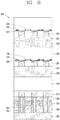
- FIGS. 7 and 8 are concept views showing the partition walls passing through the semiconductor light emitting modules
- FIG. 9 is a concept view showing the arrangement of the partition walls and the electrode lines provided in the lamp according to the present invention.
- At least one of the semiconductor light emitting devices provided in each of the light emitting modules may be disposed between any one of the partition walls and another partition wall facing that partition wall.
- any one of the two light emitting modules shown in FIG. 7 may have a semiconductor light emitting device that emits red light and the other may have semiconductor light emitting devices that emit green and blue light.
- the semiconductor light emitting device emitting red light is preferably disposed on the bottommost layer of the lamp. It is because the semiconductor light emitting device that emits the red light is the most heat-sensitive one among the semiconductor light emitting devices that emit red, green and blue light.
- the second semiconductor light emitting module may include a semiconductor light emitting device that emits red light
- the first semiconductor light emitting module may include semiconductor light emitting devices that emit green and blue light.
- each of the three semiconductor light emitting modules shown in FIG. 8 may have a semiconductor light emitting device that emits any one of red, green and blue light.
- the semiconductor light emitting device that emits the red light is preferably disposed on the bottommost layer.
- the second semiconductor light emitting module may include the semiconductor light emitting device that emits the red light.
- the electrode lines provided in the second semiconductor light emitting module are formed on the lower side of the semiconductor light emitting device, passing through the substrate, so that the electrode lines and the partition walls may not overlap with each other.
- the semiconductor light emitting device provided in the semiconductor light emitting module is a vertical type light emitting device
- the first electrode line 120 and the second electrode line 140 may be formed on different planes.
- the hole through which the first electrode line 120 passes and the hole through which the second electrode line 140 passes may be arranged on the different planes.
- FIGS. 10 to 12 are sectional concept views showing the lamp according to the present invention.
- FIGS. 10 and 11 show only the semiconductor light emitting devices and partition walls, but the lamp may include the components (not shown) explained with reference to FIG. 6 .
- the semiconductor light emitting device provided in each of the semiconductor light emitting modules may be formed without overlapping with each other. This can maximize an intensity of light of the lamp.
- the semiconductor light emitting devices provided in each of the semiconductor light emitting modules may be arranged in a stair manner.
- the semiconductor light emitting devices provided in each of the semiconductor light emitting modules may be arranged in a random manner.
- the partition wall when the partition wall is manufactured during the manufacture of the semiconductor light emitting module, the partition wall may not be formed between the semiconductor light emitting modules. Specifically, when the semiconductor light emitting module is stacked, a transparent adhesive layer may be disposed between the semiconductor light emitting modules. In this case, no partition wall is formed on the transparent adhesive layer, and light leakage to the transparent adhesive layer may occur.
- each of the partition walls may have a first partition wall part passing through each of the semiconductor light emitting modules and a second partition wall part formed between the semiconductor light emitting modules.
- the partition wall may include a first partition wall part 411 and a second partition wall part 412.
- the first partition wall part 411 may be manufactured during the manufacture of the semiconductor light emitting module.
- the second partition wall part 412 may be formed during the attachment of the two semiconductor light emitting modules.
- the second partition wall part may serve as a mold for the adhesive material.
- the second partition wall part may be made of a metal material or a material with high reflectivity, such as TiO 2 and Al 2 O 3 .
- the present invention is not limited thereto, and the second partition wall part may be made of all types of materials with a certain degree of reflexivity.
- the partition wall part when the partition wall part is disposed between the semiconductor light emitting devices, it is not only possible to light or flicker only a portion of the lamp but also implement various colors in the single lamp.
- a voltage may be selectively applied to at least one of the semiconductor light emitting devices disposed between any one of the partition walls and another partition wall facing that partition wall, so that the semiconductor light emitting device can selectively emit light. As such, it is possible to light or flicker only some of the light emitting regions of the lamp.
- selectively applying a voltage to the semiconductor light emitting device that emits a specific color of light enables the lamp to emit that specific color of light.
- light beams emitted from the lamp according to the present invention may be irradiated in different directions according to their colors.
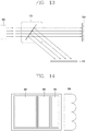
- FIG. 13 is a concept view showing a polarized beam splitter and an optical filter lay er provided in the lamp according to the present invention.
- the lamp disposed in the vehicle can perform two major functions.
- the vehicle lamp according to the present invention irradiates a certain intensity of light to the front of the vehicle to secure the view of the driver.
- the color of the irradiated light is limited so as not to interfere with the view of other drivers.
- light irradiated to secure the view of the driver is limited to white light. Light other than the white light should not be irradiated to the front of the vehicle.
- the vehicle lamp according to the present invention serves to communicate with pedestrians or other drivers. Specifically, it is possible to communicate with pedestrians or other drivers by irradiating certain signals to a road surface around the vehicle. For example, when a pedestrian tries to cross a road which is not a crosswalk, a crosswalk-shaped signal may be irradiated to the road surface to inform that the pedestrian may cross the road. Light other than the white light may be used for the aforementioned communication.
- the polarized beam splitter and optical filter layer 500 may be disposed at the front of the lamp. Specifically, the polarized beam splitter separates some of the light beams emitted from the light emitting modules to change their proceeding directions. Meanwhile, the optical filter layer blocks a certain wavelength of light. This prevents light other than white light from being irradiated to the front of the vehicle. In addition, this allows a certain wavelength of light to be irradiated around the vehicle.
- the polarized beam splitter and optical filter layer 500 When the polarized beam splitter and optical filter layer 500 are combined, it can separate some of the light beams emitted from the lamp and irradiate them in a certain direction. According to the present invention, it is thus possible to irradiate light to a road surface 510 around the vehicle and at the same time to irradiate a certain intensity of white light to the front 520 of the vehicle.
- the polarized beam splitter may be rotatable.
- the present invention proposes a structure configured such that parallel light is incident on the polarized beam splitter and optical filter layer.
- FIG. 14 is a concept view showing a lamp having a light mixing layer and a microlens array.
- the light emitting region of the lamp 300 may overlap with the light mixing layer 600 and the microlens array 700.
- the light mixing layer 600 increases an optical path to mix light beams emitted from different semiconductor light emitting modules.
- the microlens array 700 allows light passing through the light mixing layer 600 to be parallel light.
- the above-described light mixing layer 600 and microlens array 700 allow parallel light to be incident on the polarized beam splitter and optical filter layer.
- the vehicle lamp described above can selectively light and flicker some of the light emitting regions or selectively output a certain color of light. That is, the lamp according to the present invention can control lighting and flickering in pixel units or adjust the colors of the pixels.
- the lamp according to the present invention allows light beams emitted from the single light emitting region to be irradiated to different regions. As such, the lamp can be used to secure the view of the driver and to communicate with pedestrians or other drivers.
- the present invention proposes a controlling method as follows.
- the controlling method of the present invention includes: applying a voltage to each of the semiconductor light emitting devices included in each of the pixels to emit light, so that white light can be emitted from the lamp; receiving an information display request on the road surface from the user; intercepting the voltage applied to at least some of the semiconductor light emitting devices included in some of the pixels, so that light having a different color than the white light can be output from some of the pixels, upon the receipt of the information display request; and increasing the amplitude of the voltage applied to the semiconductor light emitting devices whose voltage has not been intercepted, among the semiconductor light emitting devices included in some of the pixels, so that the intensity of light of some of the pixels can increase, when the voltage applied to at least some of the semiconductor light emitting devices is intercepted.
- the present method upon the receipt of the information display request, intercepts the voltage to the semiconductor light emitting devices provided in some of the pixels.
- the present method increases the amplitude of the voltage applied to the semiconductor light emitting devices whose voltage is not intercepted by the information display request, thereby increasing the brightness of the semiconductor light emitting devices.
- the present invention can compensate for an optical loss caused by the information display.
- a controlling method of vehicle lamp comprises: a plurality of semiconductor light emitting modules vertically stacked with each other and having a substrate and a plurality of semiconductor light emitting devices disposed on the substrate; and partition walls formed between the semiconductor light emitting devices and passing through each of the semiconductor light emitting modules in a thickness direction, wherein each of the semiconductor light emitting modules has the semiconductor light emitting devices that emit different wavelengths of light.
- the vehicle lamp further comprises first and second electrode lines electrically connected to each of the plurality of semiconductor light emitting devices, wherein each of the semiconductor light emitting modules has first and second electrodes.
- the partition walls have holes through which the first and second electrode lines pass that are provided in at least one of the semiconductor light emitting modules, except the semiconductor light emitting module stacked on the bottommost layer.
- the first and second electrode lines provided in the semiconductor light emitting module stacked on the bottommost layer, among the semiconductor light emitting modules are disposed on the lower side of the semiconductor light emitting device provided in the semiconductor light emitting module stacked on the bottommost layer and pass through the substrate provided in the semiconductor light emitting module stacked on the bottommost layer.
- the semiconductor light emitting modules are composed of two semiconductor light emitting modules stacked with each other.
- any one of the two semiconductor light emitting modules has the semiconductor light emitting device that emits red light
- the other semiconductor light emitting module has the semiconductor light emitting device that emits green light and the semiconductor light emitting device that emits blue light.
- the semiconductor light emitting devices provided in any one of the semiconductor light emitting modules emit the same wavelength of light.
- the semiconductor light emitting modules are composed of three semiconductor light emitting modules stacked with each other, and the three semiconductor light emitting modules have the semiconductor light emitting device that emits the red, green and blue light, respectively.
- the semiconductor light emitting module having the semiconductor light emitting device that emits the red light, among the three semiconductor light emitting modules, is disposed on the bottommost layer, among the three semiconductor light emitting modules.
- each of the partition walls has a first partition wall part passing through each of the semiconductor light emitting modules and a second partition wall part formed between the semiconductor light emitting modules.
- the vehicle lamp further comprising a transparent adhesive layer disposed between the semiconductor light emitting modules, wherein the transparent adhesive layer is disposed between different second partition wall parts.
- the second partition wall part is formed in a mesh type.
- a voltage is applied to at least one of the semiconductor light emitting devices disposed between any one of the partition walls and another partition wall facing that partition wall, so that the semiconductor light emitting device can selectively emit light.
- the vehicle lamp further comprises a polarized beam splitter overlapping with the semiconductor light emitting modules and separating some of the light beams emitted from the semiconductor light emitting modules to change their proceeding directions.
- the polarized beam splitter is rotatable.
- the vehicle lamp comprises an optical filter layer disposed to overlap with the polarized beam splitter and blocking a certain wavelength of light.
- the vehicle lamp further comprises a light mixing layer overlapping with the semiconductor light emitting modules and mixing light beams emitted from the semiconductor light emitting modules.
Landscapes
- Engineering & Computer Science (AREA)
- General Engineering & Computer Science (AREA)
- Physics & Mathematics (AREA)
- Optics & Photonics (AREA)
- Microelectronics & Electronic Packaging (AREA)
- Mathematical Physics (AREA)
- Mechanical Engineering (AREA)
- General Physics & Mathematics (AREA)
- Spectroscopy & Molecular Physics (AREA)
- Led Devices (AREA)
- Led Device Packages (AREA)
- Non-Portable Lighting Devices Or Systems Thereof (AREA)
Abstract
Description
- The present invention relates to a vehicle lamp and a method for controlling the same and in more particularly to a vehicle lamp using a semiconductor light emitting device.
- A vehicle is equipped with a variety of vehicle lamps having a lighting function or a signal function. Generally, a halogen lamp or a gas discharge lamp has been mainly used, but in recent years, a light emitting diode (LED) has attracted attention as a light source of the vehicle lamp.
- The light emitting diode (LED) is minimized in size, which not only increases a degree of design freedom of the lamp, but also has economical efficiency by virtue of a semi-permanent lifetime. However, it is mostly manufactured in a package type. The light emitting diode (LED) itself, not a package, is a semiconductor light emitting device for converting current into light and has been developed as a light source for display images of an electronic device including information communication equipment.
- However, since the vehicle lamp developed up to now uses a package type light emitting diode, there are disadvantages in that the yield is low, the cost is high and the degree of flexibility is low.
- Meanwhile, as the demand for an intelligent lamp increases, a structure capable of selectively lighting a portion of the lamp has been developed. Therefore, a structure that prevents light beams emitted from each of a plurality of light emitting devices included in the lamp from interfering with each other has been developed.
- An object of the present invention is to provide a vehicle lamp having a structure in which semiconductor light emitting devices are vertically stacked.
- Another object of the present invention is to provide a structure capable of selectively lighting or flickering only some of the light emitting regions of a vehicle lamp.
- A further object of the present invention is to provide a structure configured such that various colors of light can be emitted from a single lamp and a method for controlling the same.
- A still further object of the present invention is to provide a structure configured such that light beams emitted from a single lamp can be directed toward the front of a vehicle and a road surface around the vehicle, respectively.
- The invention is defined by the independent claims. Dependent claims refer to preferred embodiments.
- According to the invention, a vehicle lamp is provided, comprising a plurality of semiconductor light emitting modules vertically stacked with each other and having a substrate and a plurality of semiconductor light emitting devices disposed on the substrate; and partition walls formed between the semiconductor light emitting devices and passing through each of the semiconductor light emitting modules in a thickness direction, wherein each of the semiconductor light emitting modules has the semiconductor light emitting devices to emit different wavelengths of light.
- Preferably, the vehicle lamp further comprises first and second electrode lines electrically connected to each of the plurality of semiconductor light emitting devices, wherein each of the semiconductor light emitting modules has first and second electrodes.
- Preferably, the partition walls have holes through which the first and second electrode lines pass, wherein particularly the first and second electrode lines are provided in at least one of the semiconductor light emitting modules, except the semiconductor light emitting module stacked on a bottommost layer.
- Preferably, the first and second electrode lines provided in the semiconductor light emitting module stacked on a bottommost layer, among the semiconductor light emitting modules, are disposed on a lower side of the semiconductor light emitting device provided in the semiconductor light emitting module stacked on the bottommost layer and pass through the substrate provided in the semiconductor light emitting module stacked on the bottommost layer.
- Preferably, at least one of the semiconductor light emitting devices provided in each of the semiconductor light emitting modules is disposed between any one of the partition walls and another partition wall facing that partition wall.
- Preferably, the semiconductor light emitting modules are composed of two semiconductor light emitting modules stacked with each other.
- Preferably, any one of the two semiconductor light emitting modules has the semiconductor light emitting device that is configured to emit red light, and the other semiconductor light emitting module has the semiconductor light emitting device that is configured to emit green light and the semiconductor light emitting device that is configured to emit blue light.
- Preferably, the semiconductor light emitting devices provided in any one of the semiconductor light emitting modules are configured to emit the same wavelength of light.
- Preferably, the semiconductor light emitting modules are composed of three semiconductor light emitting modules stacked with each other, and the three semiconductor light emitting modules have the semiconductor light emitting device to emit the red, green and blue light, respectively.
- Preferably, each of the partition walls has a first partition wall part passing through each of the semiconductor light emitting modules and a second partition wall part formed between the semiconductor light emitting modules.
- Preferably, the vehicle lamp further comprises a transparent adhesive layer disposed between the semiconductor light emitting modules, wherein the transparent adhesive layer is disposed between different second partition wall parts.
- Preferably, the vehicle lamp is configured such that, if a voltage is applied to at least one of the semiconductor light emitting devices disposed between any one of the partition walls and another partition wall facing that partition wall, at least one of the semiconductor light emitting device will selectively emit light.
- Preferably, the vehicle lamp further comprises a polarized beam splitter overlapping with the semiconductor light emitting modules and configured to separate at least some of the light beams emitted from the semiconductor light emitting modules to change their proceeding directions.
- Preferably, the vehicle lamp further comprises a light mixing layer overlapping with the semiconductor light emitting modules and configured to mix light beams emitted from the semiconductor light emitting modules.
- According to the invention, a method is further provided for controlling a vehicle lamp comprising a plurality of pixels having semiconductor light emitting devices that emit red, green and blue light, comprising: applying a voltage to each of the semiconductor light emitting devices included in each of the pixels to emit light, so that white light is emitted from the vehicle lamp; receiving an information display request to display information on a road surface; intercepting the voltage applied to at least some of the semiconductor light emitting devices included in some of the pixels, so that light having a different color than the white light can be output from some of the pixels, upon the receipt of the information display request; and increasing the amplitude of the voltage applied to the semiconductor light emitting devices whose voltage has not been intercepted, among the semiconductor light emitting devices included in some of the pixels, so that the intensity of light of some of the pixels can increase, when the voltage applied to at least some of the semiconductor light emitting devices is intercepted.
- In order to achieve the above-described objects, according to an aspect of the present invention, there is provided a vehicle lamp, comprising: a plurality of semiconductor light emitting modules vertically stacked with each other and having a substrate and a plurality of semiconductor light emitting devices disposed on the substrate; and partition walls formed between the semiconductor light emitting devices and passing through each of the semiconductor light emitting modules in a thickness direction, wherein each of the light emitting modules has the semiconductor light emitting devices that emit different wavelengths of light.
- In some embodiments, the vehicle lamp may further comprise first and second electrode lines electrically connected to each of the plurality of semiconductor light emitting devices, wherein each of the light emitting modules may have the first and second electrodes.
- In some embodiments, the partition walls may have holes through which the first and second electrode lines pass that are provided in at least one of the light emitting modules, except the light emitting module stacked on the bottommost layer.
- In some embodiments, the first and second electrode lines provided in the light emitting module stacked on the bottommost layer, among the light emitting modules, may be disposed on the lower side of the semiconductor light emitting device provided in the light emitting module stacked on the bottommost layer and may pass through the substrate provided in the light emitting module stacked on the bottommost layer.
- In some embodiments, at least one of the semiconductor light emitting devices provided in each of the light emitting modules may be disposed between any one of the partition walls and another partition wall facing that partition wall.
- In some embodiments, the light emitting modules may be composed of two light emitting modules stacked with each other.
- In some embodiments, any one of the two light emitting modules may have the semiconductor light emitting device that emits red light, and the other light emitting module may have the semiconductor light emitting device that emits green light and the semiconductor light emitting device that emits blue light.
- In some embodiments, the semiconductor light emitting devices provided in any one of the light emitting modules may emit the same wavelength of light.
- In some embodiments, the light emitting modules may be composed of three light emitting modules stacked with each other, and each of the three light emitting modules may have the semiconductor light emitting device that emits any one of the red, green and blue light.
- In some embodiments, the light emitting module having the semiconductor light emitting device that emits the red light, among the three light emitting modules, may be disposed on the bottommost layer, among the three light emitting modules.
- In some embodiments, the semiconductor light emitting devices included in each of the light emitting module do not overlap with each other.
- In some embodiments, each of the partition walls may have a first partition wall part passing through each of the semiconductor light emitting modules and a second partition wall part formed between the semiconductor light emitting modules.
- In some embodiments, the vehicle lamp may further comprise a transparent adhesive layer disposed between the light emitting modules, wherein the transparent adhesive layer may be disposed between different second partition wall parts.
- In some embodiments, the first and second partition wall parts may overlap with each other.
- In some embodiments, the second partition wall part may be formed in a mesh type.
- In some embodiments, a voltage may be applied to at least one of the semiconductor light emitting devices disposed between any one of the partition walls and another partition wall facing that partition wall, so that the semiconductor light emitting device can selectively emit light.
- In some embodiments, the vehicle lamp may further comprise a polarized beam splitter overlapping with the light emitting modules and separating some of the light beams emitted from the light emitting modules to change their proceeding directions.
- In some embodiments, the polarized beam splitter may be rotatable.
- In some embodiments, the vehicle lamp may further comprise an optical filter layer disposed to overlap with the polarized beam splitter and blocking a certain wavelength of light.
- In some embodiments, the vehicle lamp may further comprise a light mixing layer overlapping with the light emitting modules and mixing light beams emitted from the light emitting modules.
- In addition, according to another aspect of the present invention, there is provided a method for controlling a vehicle lamp comprising a plurality of pixels having semiconductor light emitting devices that emit red, green and blue light. In a specific embodiment, the controlling method of the present invention may comprise: applying a voltage to each of the semiconductor light emitting devices included in each of the pixels to emit light, so that white light can be emitted from the lamp; receiving an information display request on a road surface from the user; intercepting the voltage applied to at least some of the semiconductor light emitting devices included in some of the pixels, so that light having a different color than the white light can be output from some of the pixels, upon the receipt of the information display request; and increasing the amplitude of the voltage applied to the semiconductor light emitting devices whose voltage has not been intercepted, among the semiconductor light emitting devices included in some of the pixels, so that the intensity of light of some of the pixels can increase, when the voltage applied to at least some of the semiconductor light emitting devices is intercepted.
- According to the present invention, it is not necessary to transfer different types of semiconductor light emitting devices to one substrate, which leads to a reduced transfer time.
- In addition, according to the present invention, the partition walls are disposed between the vertically-stacked semiconductor light emitting devices, which increases a contrast effect between the semiconductor light emitting devices. As such, it is possible to selectively light or flicker some of the light emitting regions of the lamp.
- Moreover, according to the present invention, light beams vertically stacked with each other are mixed and emitted to the outside, which makes it possible to implement various colors in the single lamp.
- Further, according to the present invention, since the proceeding directions of som e of the light beams emitted from the light emitting regions can be changed, the single lam p can be used not only as the means for securing the view of the driver but also the means for communicating with pedestrians or other drivers.
- In addition, according to an aspect of the present invention, there is provided a vehicle in which the vehicle lamp of the present invention is used.
- The accompanying drawings, which are included to provide a further understanding of the invention and are incorporated in and constitute a part of this specification, illustrate exemplary embodiments and together with the description serve to explain the principles of the invention.
- In the drawings:
-
FIG. 1 is a concept view showing one embodiment of a vehicle lamp using a semiconductor light emitting device of the present invention. -
FIG. 2 is a partial enlarged view of part A ofFIG. 1 andFIG. 3 is a sectional view. -
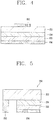
FIG. 4 is a concept view showing a vertical type semiconductor light emitting device. -
FIG. 5 is a concept view showing a flip chip type semiconductor light emitting device. -
FIG. 6 is a sectional view of a vehicle lamp according to the present invention. -
FIGS. 7 and 8 are concept views showing partition walls passing through semiconductor light emitting modules. -
FIG. 9 is a concept view showing the arrangement of partition walls and electrode lines provided in the lamp according to the present invention. -
FIGS. 10 to 12 are concept views showing partition walls formed in each semiconductor light emitting module. -
FIG. 13 is a concept view showing a polarized beam splitter and an optical filter lay er provided in the lamp according to the present invention. -
FIG. 14 is a concept view showing a lamp having a light mixing layer and a microlens array. - Hereinafter, embodiments of the present invention will be described in detail with reference to the accompanying drawings, wherein identical reference numerals are used to designate identical or similar elements, and a description thereof will be omitted. The terms "module" and "parts" for the components in the following description are given or mixed merely in terms of the ease of preparing the specification, and do not have their own distinguishable meanings or functions. In addition, in the following description of the embodiments of the present invention, a detailed description of the related arts will be omitted in order not to unnecessarily obscure the present invention. Moreover, it should be noted that the accompanying drawings are given only for a better understanding of the embodiments disclosed herein and are not be construed as limiting the technical ideas disclosed herein.
- It will also be understood that when an element such as a layer, region or substrate is referred to as being present "on" another element, it may be directly on another element or an intermediate element may be present therebetween.
- A vehicle lamp described herein may include a headlamp, a tail lamp, a vehicle light, a fog light, a direction indicating lamp, a brake light, an emergency light, a rear lamp, and the like. However, it will be readily apparent to those skilled in the art that the configuration according to the embodiments described herein may be applied to a new product to be developed in the future, so far as it has a display function.
-
FIG. 1 is a concept view showing one embodiment of a vehicle lamp using a semiconductor light emitting device of the present invention. - The
vehicle lamp 10 according to the embodiment of the present invention includes aframe 11 fixed to a vehicle body and alight source part 12 installed on theframe 11. - A wiring line for supplying power to the
light source part 12 is connected to theframe 11, and theframe 11 may be fastened to the body directly or via a bracket. As shown, a lens unit may be provided in order for light emitted from thelight source part 12 to be more clear and easily diffused. - The
light source part 12 may be a flexible light source part that can be bent, curved, twisted, folded, and rolled by an external force. - When the
light source part 12 is not bent (for example, when it has an infinite radius of curvature; hereinafter, referred to as a first state), it becomes a plane. When thelight source part 12 is bent due to an external force in the first state (for example, when it has a finite radius of curvature; hereinafter, referred to as a second state), the flexible light source part may be at least partially bent or curved. - A pixel of the
light source part 12 may be implemented by a semiconductor light emitting device. In the present invention, a light emitting diode LED is given as an example of a semiconductor light emitting device that converts current into light. The light emitting diode is formed in a small size and can serve as a pixel in the second state. - Meanwhile, the
light source part 12 according to the present invention includes a unit light source, a base substrate, and a connecting electrode. These components will be described below in detail. - The
light source part 12 may be only composed of the unit light source. The unit light source will be described below in detail through thelight source part 12 only composed of the unit light source. -
FIG. 2 is a partial enlarged view of part A ofFIG. 1 ,FIG. 3 is a sectional view,FIG. 4 is a concept view showing a vertical type semiconductor light emitting device, andFIG. 5 is a concept view showing a flip chip type semiconductor light emitting device. - As shown in
FIGS. 2, 3 and4 , a passive matrix (PM) type semiconductor light emitting device is used as aunit light source 100 using a semiconductor light emitting device. However, the following description is also applicable to an active matrix (AM) type semiconductor light emitting device. - The
unit light source 100 includes asubstrate 110, afirst electrode 120, a firstadhesive layer 130, asecond electrode 140, and a plurality of semiconductorlight emitting devices 150. - The
substrate 110 is a base layer on which the structure is formed through the whole process and may be a wiring substrate on which thefirst electrode 120 is disposed. Thesubstrate 110 may include glass or polyimide (PI) to implement a flexible light source part. In addition, thesubstrate 110 may be made of a thin metal. Any type of insulating and flexible material, e.g., polyethylene naphthalate (PEN) and polyethylene terephthalate (PET) may be used. Furthermore, thesubstrate 110 may be either transparent or opaque. - In the meantime, a heat-radiating sheet or heat sink may be mounted on the
substrate 110 to implement a heat-radiating function. In this case, the heat-radiating sheet or heat sink may be mounted on the opposite surface to the surface having thefirst electrode 120 thereon. - The
first electrode 120 may be positioned on thesubstrate 110 and provided as a planar electrode. Therefore, thefirst electrode 120 may be an electrode layer disposed on the substrate and can serve as a data electrode. Meanwhile, an electrode pad 123 for facilitating an electrical connection to the connecting electrode 220 may be disposed on thefirst electrode 120. - The first
adhesive layer 130 is formed on thesubstrate 110 having thefirst electrode 120 thereon. - The first
adhesive layer 130 may be a layer with adhesiveness and conductivity. To this end, the firstadhesive layer 130 may be made of a mixture of a conductive material and an adhesive material. Accordingly, the first adhesive layer may be referred to as a conductive first adhesive layer. Also, the firstadhesive layer 130 has ductility, which makes it possible for the light source part to have a flexible function. - As an example, the first
adhesive layer 130 may be an anisotropy conductive film (ACF), an anisotropy conductive paste, a solution containing conductive particles, and the like. The firstadhesive layer 130 may be provided as a layer allowing an electrical connection in a vertical Z direction but having an electric insulation in a horizontal X-Y direction. Thus, the firstadhesive layer 130 may be called as a Z-axis conductive layer. - The anisotropy conductive film is made of a mixture of an anisotropy conductive medium and an insulating base member, such that, when heat and pressure are applied thereto, only specific portions have conductivity due to the anisotropy conductive medium. In the following description, heat and pressure are applied to the anisotropy conductive film, but different methods can be used to make the anisotropy conductive film partially conductive. For example, this methods may include the application of either heat or pressure or UV curing.
- In addition, the anisotropy conductive medium may be a conductive ball or conductive particle, for example. As shown, in this example, the anisotropy conductive film is made of a mixture of a conductive ball and an insulating base member, such that, when heat and pressure are applied thereto, only specific portions have conductivity due to the conductive ball. The anisotropy conductive film may include a plurality of particles in which a conductive core is coated with an insulating film made of a polymer material. In this case, the insulating film of the heat and pressure-applied portion is destroyed and the core provides conductivity. Here, the shape of the core may be modified to form layers contacting each other in the thickness direction of the film. As a more specific example, heat and pressure are applied to the entire anisotropy conductive film, and an electrical connection in the Z-axis direction is partially formed due to a height difference of an object adhered by the anisotropy conductive film.
- As another example, the anisotropy conductive film may include a plurality of particles in which an insulating core is coated with a conductive material. In this case, the conductive material of the heat and pressure-applied portion is deformed (stuck) to have conductivity in the thickness direction of the film. As a further example, the conductive material may pass through the insulating base member in the Z-axis direction to have conductivity in the thickness direction of the film. In this case, the conductive material may have a pointed end.
- As shown, the anisotropy conductive film may be a fixed array ACF in which a conductive ball is inserted into one surface of the insulating base member. More specifically, the insulating base member is made of a material with adhesiveness, and the conductive ball is intensively disposed on the bottom of the insulating base member, such that, when heat and pressure are applied to the base member, it is deformed together with the conductive ball to have conductivity in the vertical direction.
- However, the present invention is not limited thereto, but the anisotropy conductive film may be configured such that the conductive ball is randomly incorporated into the insulating base member or may be composed of a plurality of layers, with the conductive ball disposed on any one of the layers (double-ACF).
- The anisotropy conductive paste, which is a combined form of a paste and a conductive ball, may be made of a mixture of an insulating and adhesive base material and a conductive ball. In addition, the solution containing the conductive particles may contain conductive particles or nano particles.
- When the
first electrode 120 is positioned on thesubstrate 110, for example, the anisotropy conductive film is positioned thereon, and then heat and pressure are applied thereto to connect the semiconductorlight emitting device 150, so that the semiconductorlight emitting device 150 is electrically connected to thefirst electrode 120. Here, the semiconductorlight emitting device 150 is preferably positioned on thefirst electrode 120. In addition, since the anisotropy conductive film contains adhesive components, the firstadhesive layer 130 implements an electrical connection as well as a mechanical connection between the semiconductorlight emitting device 150 and thefirst electrode 120. - As a further example, the first adhesive layer may include Tin alloy, Au, Al, or Pb for eutectic bonding, and the substrate and the semiconductor light emitting device may be coupled to each other by means of the eutectic bonding.
- The semiconductor
light emitting device 150 has excellent brightness, and thus can compose an individual unit pixel in a small size. Such an individual semiconductorlight emitting device 150 may be a rectangular or square device in which one side has a length of 80 µm or less. In this case, the area of the single semiconductorlight emitting device 150 may range from 10-10 to 10-5 m2 and the distance between the light emitting devices may range from 100 µm to 10 mm. - The semiconductor
light emitting device 150 may have a vertical type structure. - A plurality of
second electrodes 140 are positioned between the vertical type semiconductor light emitting devices and electrically connected thereto. - Referring to
FIG. 4 , this vertical type semiconductor light emitting device includes a p-type electrode 156, a p-type semiconductor layer 155 formed on the p-type electrode 156, anactive layer 154 formed on the p-type semiconductor layer 155, an n-type semiconductor layer 153 formed on theactive layer 154, and an n-type electrode 152 formed on the n-type semiconductor layer 153. In this case, the p-type electrode 156 positioned at the lower portion can be electrically connected to thefirst electrode 120 by the firstadhesive layer 130, and the n-type electrode 152 positioned at the upper portion can be electrically connected to thesecond electrode 140 discussed later. This vertical type semiconductor light emitting device has a significant advantage of reducing a chip size since the electrodes can be placed up and down. - Referring to
FIGS. 2 and 3 again, the plurality of semiconductorlight emitting devices 150 compose a light emitting device array, and aninsulation layer 160 is formed between the plurality of semiconductorlight emitting devices 150. For example, theinsulation layer 160 is formed on one surface of the firstadhesive layer 130 to fill the spaces between the semiconductorlight emitting devices 150. - However, the present invention is not limited thereto, and the first
adhesive layer 130 may fill the spaces between the semiconductor light emitting devices without theinsulation layer 160. - The
insulation layer 160 may be a transparent insulation layer including SiOx. As another example, polymer materials having excellent insulation and low optical absorption, such as epoxy, methyl and phenyl-based silicon, or inorganic materials such as SiN and Al2O3 may be used for theinsulation layer 160 as a structure for preventing shorts between the electrodes. - As shown, a
phosphor layer 180 is formed on the light emitting device array. - The
phosphor layer 180 may be formed on one surface of the semiconductorlight emitting device 150. For example, the semiconductorlight emitting device 150 may be a blue semiconductor light emitting device 151 emitting blue light B, and aphosphor layer 180 may be provided to convert this blue light B into a different color of light. In this case, thephosphor layer 180 may have a red phosphor capable of converting the blue light B into red light R, a green phosphor capable of converting the blue light B into green light G, or a yellow phosphor capable of converting the blue light B into white light W. - In this case, the wavelength of light generated in the nitride-based semiconductor light emitting device ranges from 390 to 550 nm, which can be converted into 450 to 670 nm through the phosphor-inserted film. In addition, both the red phosphor and the green phosphor may be provided to mix various wavelength of light to implement the white light. Moreover, when red light is required, in the case of a GaAs-based red semiconductor light emitting device, not a phosphor but a light diffusion film may be used. Further, a patterned sheet may be inserted to improve optical extraction efficiency.
- In this case, an
optical gap layer 171 may be present between the semiconductorlight emitting device 150 and thephosphor layer 180. Theoptical gap layer 171 may be formed of a material having low optical absorption and excellent bending property, such as epoxy, acryl, or methyl and phenyl-based silicon. Also, a patterned sheet may be inserted or particles having a different refractive index may be mixed for the optimization of optical efficiency. - Meanwhile, a
color filter 172 may be stacked on thephosphor layer 180 to improve color purity of the converted light. In addition, in order to protect the light source part from moisture, oxygen and external shock, aprotective layer 173 may be formed to cover thecolor filter 172. Here, theprotective layer 173 may be implemented by film bonding or resin coating. - Furthermore, referring to
FIG. 5 , the semiconductor light emitting device may be a flip chip type light emitting device. - For example, the semiconductor light emitting device includes a p-
type electrode 256, a p-type semiconductor layer 255 formed on the p-type electrode 256, anactive layer 254 formed on the p-type semiconductor layer 255, an n-type semiconductor layer 253 formed on theactive layer 254, and an n-type electrode 252 formed on the n-type semiconductor layer 253 to be spaced apart from the p-type electrode 256. In this case, the p-type electrode 256 can be electrically connected to the first electrode, and the n-type electrode 252 can be electrically connected to the second electrode. - When the semiconductor light emitting devices that emit different colors of light are disposed on the vehicle lamp described above, the single vehicle lamp can implement a variety of colors. Specifically, when the semiconductor light emitting devices that emit red, green and blue light are disposed on the lamp, respectively, the lamp can implement a variety of colors including a white color.
- However, since the semiconductor light emitting devices are very small, it is very difficult to dispose different types of light emitting devices on the same substrate. It leads to an increased manufacturing cost and time of the lamp.
- The present invention provides a vehicle lamp of a novel structure that is easy to manufacture and capable of implementing a variety of colors. Along with this, the present invention provides a vehicle lamp that is capable of lighting or flickering some of the light emitting regions of the lamp.
- Hereinafter, the present invention will be described in detail with reference to the accompanying drawings.
-
FIG. 6 is a sectional view of a vehicle lamp according to the present invention. - In the lamp according to the present invention, a plurality of semiconductor light emitting modules are vertically stacked. The light emitting module may include a substrate, a plurality of semiconductor light emitting devices, and a plurality of electrode lines. Here, the electrode lines and the plurality of semiconductor light emitting devices are electrically connected.
- Meanwhile, the lamp according to the present invention may include two types of semiconductor light emitting modules.
- The first semiconductor light emitting module is disposed at an upper layer part of the lamp. When the plurality of semiconductor light emitting modules are vertically stacked, the substrates provided in the respective semiconductor light emitting modules overlap with each other. Here, the substrates may be made of a light transmitting material so that the semiconductor light emitting module disposed on the relatively upper side does not absorb or reflect light emitted from the semiconductor light emitting module disposed on the relatively lower side.
- Referring to
FIG. 6 , the first semiconductor light emitting module may include asubstrate 330, anadhesive layer 310, a plurality of semiconductorlight emitting devices 150, and a plurality ofelectrode lines substrate 330 and theadhesive layer 310 may be made of a light transmitting material. The semiconductor light emitting device is attached to thesubstrate 330 through the transparentadhesive layer 310. - In this specification, the flip chip type semiconductor light emitting device in
FIG. 5 has been described as an example of the semiconductor light emitting device provided in the first semiconductor light emitting module, but the first semiconductor light emitting device may include the vertical type semiconductor light emitting device inFIG. 4 . - Meanwhile, the
electrode lines electrode lines electrode lines light emitting devices 150 through atransparent electrode 320. Therefore, not theelectrode lines transparent electrode 320 overlap with the semiconductorlight emitting devices 150. - In the meantime, the first semiconductor light emitting module may include a
light diffusion layer 340 so that light beams emitted from the semiconductor light emitting devices are well mixed and emitted to the outside. For example, thelight diffusion layer 340 may be made of a light transmitting polymer material such as PDMS. - Furthermore, the second semiconductor light emitting module is a light emitting module disposed on the bottommost layer of the lamp. Specifically, the second semiconductor light emitting module is disposed on a
base substrate 390. The second semiconductor light emitting module may include asubstrate 380, areflective layer 370, anadhesive layer 360, a plurality of semiconductorlight emitting devices 250, and a plurality ofelectrode lines - Since a semiconductor light emitting device is not disposed on the lower side of the second semiconductor light emitting module, the
substrate 380 is not necessarily made of a transparent material. Moreover, the electrode lines may be disposed on the lower side of the semiconductor light emitting device to prevent light directed toward the upper side of the semiconductor light emitting device from being reflected by the electrode lines. - Meanwhile, the second semiconductor light emitting module reflects the light directed toward the lower side of the lamp to be directed toward the upper side of the lamp. To this end, the second semiconductor light emitting device includes the
reflective layer 370. The reflective layer may be made of a metal or an inorganic material with high reflectivity. - In the meantime, the
electrode lines adhesive layer 360, thereflective layer 370, and thesubstrate 380. This is intended to minimize holes formed in partition walls discussed later. It will be described below. - Furthermore, the second semiconductor light emitting module may include a
light diffusion layer 340 like the first semiconductor light emitting module. - The lamp according to the present invention has a structure in which the second semiconductor light emitting module and the first semiconductor light emitting module are stacked in order or a structure in which one second semiconductor light emitting module and two first semiconductor light emitting modules are stacked in order.
- The aforementioned first semiconductor light emitting module may be separately manufactured, and then stacked with another semiconductor light emitting modules in a vertical manner. Here, the respective semiconductor light emitting modules may have semiconductor light emitting devices that emit different wavelengths of light. As such, the respective semiconductor light emitting modules can implement different colors. Using this method, it is not necessary to transfer different types of semiconductor light emitting devices to one substrate, which leads to a reduced transfer time.
- Meanwhile, the lamp according to the present invention enables a user to light or flicker only some of the light emitting regions. Specifically, in the present invention, the region in which the semiconductor light emitting device emits light is clearly distinguished from the region in which the semiconductor light emitting device does not emit light. To this end, the lamp according to the present invention includes partition walls formed between the semiconductor light emitting devices and passing through the vertically-stacked semiconductor light emitting modules.
-
FIGS. 7 and 8 are concept views showing the partition walls passing through the semiconductor light emitting modules, andFIG. 9 is a concept view showing the arrangement of the partition walls and the electrode lines provided in the lamp according to the present invention. - At least one of the semiconductor light emitting devices provided in each of the light emitting modules may be disposed between any one of the partition walls and another partition wall facing that partition wall.
- Referring to
FIG. 7 , the lamp according to the present invention may include a first semiconductor light emitting module having two types of semiconductor light emitting devices and a second semiconductor light emitting module having one type of semiconductor light emitting device. In this case, one or two semiconductor light emitting devices are disposed between the two facing partition walls. Thepartition walls 410 are disposed to pass through the first and second semiconductor light emitting modules. - In one embodiment, any one of the two light emitting modules shown in
FIG. 7 may have a semiconductor light emitting device that emits red light and the other may have semiconductor light emitting devices that emit green and blue light. Here, the semiconductor light emitting device emitting red light is preferably disposed on the bottommost layer of the lamp. It is because the semiconductor light emitting device that emits the red light is the most heat-sensitive one among the semiconductor light emitting devices that emit red, green and blue light. Accordingly, the second semiconductor light emitting module may include a semiconductor light emitting device that emits red light, and the first semiconductor light emitting module may include semiconductor light emitting devices that emit green and blue light. - Meanwhile, as shown in
FIG. 8 , the lamp according to the present invention may have a structure in which one second semiconductor light emitting module and two first semiconductor light emitting modules are stacked in order. In this case, one semiconductor light emitting device is disposed between the two facing partition walls. Here, thepartition walls 410 are disposed to pass through the three semiconductor light emitting modules. - In one embodiment, each of the three semiconductor light emitting modules shown in
FIG. 8 may have a semiconductor light emitting device that emits any one of red, green and blue light. Here, the semiconductor light emitting device that emits the red light is preferably disposed on the bottommost layer. As a result, the second semiconductor light emitting module may include the semiconductor light emitting device that emits the red light. - The
partition walls 410 may be made of a material with high reflectivity, such as TiO2 and Al2O3 or may be a polymer structure coated with a metal thin film. Since thepartition walls 410 are disposed to surround the respective sides of the semiconductor light emitting devices and pass through the semiconductor light emitting modules in a thickness direction, the electrode lines inevitably overlap with the partition walls. - As explained with reference to
FIG. 6 , the electrode lines provided in the second semiconductor light emitting module are formed on the lower side of the semiconductor light emitting device, passing through the substrate, so that the electrode lines and the partition walls may not overlap with each other. - Each of the partition walls may have holes through which the electrode lines pass that are provided in the light emitting modules, except the second light emitting module stacked on the bottommost layer of the lamp. Referring to
FIG. 9 , thefirst electrode line 120 and thesecond electrode line 140 provided in each semiconductor light emitting module may be arranged on the same plane. This arrangement may be useful when the semiconductor light emitting device provided in the semiconductor light emitting module is a flip chip type light emitting device. Here, the hole through which thefirst electrode line 120 passes and the hole through which thesecond electrode line 140 passes may be arranged on the same plane. - In the meantime, when the semiconductor light emitting device provided in the semiconductor light emitting module is a vertical type light emitting device, the
first electrode line 120 and thesecond electrode line 140 may be formed on different planes. Here, the hole through which thefirst electrode line 120 passes and the hole through which thesecond electrode line 140 passes may be arranged on the different planes. - Furthermore, the partition walls can be manufactured during the manufacture of the semiconductor light emitting module.
-
FIGS. 10 to 12 are concept views showing partition walls formed in each of the semiconductor light emitting modules. -
FIGS. 10 to 12 are sectional concept views showing the lamp according to the present invention.FIGS. 10 and11 show only the semiconductor light emitting devices and partition walls, but the lamp may include the components (not shown) explained with reference toFIG. 6 . - Meanwhile, the semiconductor light emitting device provided in each of the semiconductor light emitting modules may be formed without overlapping with each other. This can maximize an intensity of light of the lamp. Specifically, as shown in
FIG. 10 , the semiconductor light emitting devices provided in each of the semiconductor light emitting modules may be arranged in a stair manner. Conversely, as shown inFIG. 11 , the semiconductor light emitting devices provided in each of the semiconductor light emitting modules may be arranged in a random manner. - In the meantime, as shown in
FIG., 10 , when the partition wall is manufactured during the manufacture of the semiconductor light emitting module, the partition wall may not be formed between the semiconductor light emitting modules. Specifically, when the semiconductor light emitting module is stacked, a transparent adhesive layer may be disposed between the semiconductor light emitting modules. In this case, no partition wall is formed on the transparent adhesive layer, and light leakage to the transparent adhesive layer may occur. - In order to solve this problem, each of the partition walls may have a first partition wall part passing through each of the semiconductor light emitting modules and a second partition wall part formed between the semiconductor light emitting modules.
- Specifically, referring to
FIG. 12 , the partition wall may include a firstpartition wall part 411 and a secondpartition wall part 412. The firstpartition wall part 411 may be manufactured during the manufacture of the semiconductor light emitting module. On the other hand, the secondpartition wall part 412 may be formed during the attachment of the two semiconductor light emitting modules. - Specifically, the second
partition wall part 412 may be formed in a mesh type. When the mesh-type second partition wall part is disposed on the upper side of the semiconductor light emitting module and an adhesive material is applied thereto, the adhesive material is disposed between the second partition wall parts. Here, the second partition wall part should be disposed to overlap with the first partition wall part. Then, the aforementioned semiconductor light emitting module and another semiconductor light emitting module are stacked, so that the two semiconductor light emitting modules are attached and at the same time the second partition wall part is formed. - As described above, in the process of attaching the two semiconductor light emitting modules, the second partition wall part may serve as a mold for the adhesive material.
- The second partition wall part may be made of a metal material or a material with high reflectivity, such as TiO2 and Al2O3. However, the present invention is not limited thereto, and the second partition wall part may be made of all types of materials with a certain degree of reflexivity.
- As described above, when the partition wall part is disposed between the semiconductor light emitting devices, it is not only possible to light or flicker only a portion of the lamp but also implement various colors in the single lamp.
- In one embodiment, a voltage may be selectively applied to at least one of the semiconductor light emitting devices disposed between any one of the partition walls and another partition wall facing that partition wall, so that the semiconductor light emitting device can selectively emit light. As such, it is possible to light or flicker only some of the light emitting regions of the lamp. In addition, selectively applying a voltage to the semiconductor light emitting device that emits a specific color of light enables the lamp to emit that specific color of light.
- Meanwhile, light beams emitted from the lamp according to the present invention may be irradiated in different directions according to their colors.
-
FIG. 13 is a concept view showing a polarized beam splitter and an optical filter lay er provided in the lamp according to the present invention. - The lamp disposed in the vehicle can perform two major functions.
- First, the vehicle lamp according to the present invention irradiates a certain intensity of light to the front of the vehicle to secure the view of the driver. When the lamp performs this function, the color of the irradiated light is limited so as not to interfere with the view of other drivers. For example, light irradiated to secure the view of the driver is limited to white light. Light other than the white light should not be irradiated to the front of the vehicle.
- Second, the vehicle lamp according to the present invention serves to communicate with pedestrians or other drivers. Specifically, it is possible to communicate with pedestrians or other drivers by irradiating certain signals to a road surface around the vehicle. For example, when a pedestrian tries to cross a road which is not a crosswalk, a crosswalk-shaped signal may be irradiated to the road surface to inform that the pedestrian may cross the road. Light other than the white light may be used for the aforementioned communication.
- As shown in
FIG. 13 , in order for the single lamp to perform the above two functions, the polarized beam splitter andoptical filter layer 500 may be disposed at the front of the lamp. Specifically, the polarized beam splitter separates some of the light beams emitted from the light emitting modules to change their proceeding directions. Meanwhile, the optical filter layer blocks a certain wavelength of light. This prevents light other than white light from being irradiated to the front of the vehicle. In addition, this allows a certain wavelength of light to be irradiated around the vehicle. - When the polarized beam splitter and
optical filter layer 500 are combined, it can separate some of the light beams emitted from the lamp and irradiate them in a certain direction. According to the present invention, it is thus possible to irradiate light to aroad surface 510 around the vehicle and at the same time to irradiate a certain intensity of white light to thefront 520 of the vehicle. Here, in order to adjust the position of the road surface to which light is irradiated, the polarized beam splitter may be rotatable. - In the meantime, in order to facilitate the above light splitting, light incident on the polarized beam splitter and
optical filter layer 500 should be parallel. Thus, the present invention proposes a structure configured such that parallel light is incident on the polarized beam splitter and optical filter layer. -
FIG. 14 is a concept view showing a lamp having a light mixing layer and a microlens array. - As shown in
FIG. 14 , the light emitting region of thelamp 300 may overlap with thelight mixing layer 600 and themicrolens array 700. Thelight mixing layer 600 increases an optical path to mix light beams emitted from different semiconductor light emitting modules. Meanwhile, themicrolens array 700 allows light passing through thelight mixing layer 600 to be parallel light. The above-describedlight mixing layer 600 andmicrolens array 700 allow parallel light to be incident on the polarized beam splitter and optical filter layer. - The vehicle lamp described above can selectively light and flicker some of the light emitting regions or selectively output a certain color of light. That is, the lamp according to the present invention can control lighting and flickering in pixel units or adjust the colors of the pixels.
- Meanwhile, the lamp according to the present invention allows light beams emitted from the single light emitting region to be irradiated to different regions. As such, the lamp can be used to secure the view of the driver and to communicate with pedestrians or other drivers.
- In order to secure the view of the driver, a certain intensity of light should be irradiated to the front of the vehicle. While light is irradiated to the front of the vehicle to secure the view of the driver, if the lamp is used as a communication means, the intensity of the light for securing the view of the driver may be instantaneously reduced. To solve this problem, the present invention proposes a controlling method as follows.
- Specifically, the controlling method of the present invention includes: applying a voltage to each of the semiconductor light emitting devices included in each of the pixels to emit light, so that white light can be emitted from the lamp; receiving an information display request on the road surface from the user; intercepting the voltage applied to at least some of the semiconductor light emitting devices included in some of the pixels, so that light having a different color than the white light can be output from some of the pixels, upon the receipt of the information display request; and increasing the amplitude of the voltage applied to the semiconductor light emitting devices whose voltage has not been intercepted, among the semiconductor light emitting devices included in some of the pixels, so that the intensity of light of some of the pixels can increase, when the voltage applied to at least some of the semiconductor light emitting devices is intercepted.
- Only some of the whole pixels included in the lamp should be lit to display information on the road surface around the vehicle. To this end, according to the present invention, upon the receipt of the information display request, the present method intercepts the voltage to the semiconductor light emitting devices provided in some of the pixels.
- Accordingly, the intensity of light for securing the view of the driver may be reduced. To prevent this problem, the present method increases the amplitude of the voltage applied to the semiconductor light emitting devices whose voltage is not intercepted by the information display request, thereby increasing the brightness of the semiconductor light emitting devices. As such, the present invention can compensate for an optical loss caused by the information display.
- A controlling method of vehicle lamp is provided, the vehicle lamp comprises: a plurality of semiconductor light emitting modules vertically stacked with each other and having a substrate and a plurality of semiconductor light emitting devices disposed on the substrate; and partition walls formed between the semiconductor light emitting devices and passing through each of the semiconductor light emitting modules in a thickness direction, wherein each of the semiconductor light emitting modules has the semiconductor light emitting devices that emit different wavelengths of light.
- According to the controlling method, the vehicle lamp further comprises first and second electrode lines electrically connected to each of the plurality of semiconductor light emitting devices, wherein each of the semiconductor light emitting modules has first and second electrodes.
- According to the controlling method, wherein the partition walls have holes through which the first and second electrode lines pass that are provided in at least one of the semiconductor light emitting modules, except the semiconductor light emitting module stacked on the bottommost layer.
- According to the controlling method, wherein the first and second electrode lines provided in the semiconductor light emitting module stacked on the bottommost layer, among the semiconductor light emitting modules, are disposed on the lower side of the semiconductor light emitting device provided in the semiconductor light emitting module stacked on the bottommost layer and pass through the substrate provided in the semiconductor light emitting module stacked on the bottommost layer.
- According to the controlling method, wherein at least one of the semiconductor light emitting devices provided in each of the semiconductor light emitting modules is disposed between any one of the partition walls and another partition wall facing that partition wall.
- According to the controlling method, wherein the semiconductor light emitting modules are composed of two semiconductor light emitting modules stacked with each other.
- According to the controlling method,wherein any one of the two semiconductor light emitting modules has the semiconductor light emitting device that emits red light, and the other semiconductor light emitting module has the semiconductor light emitting device that emits green light and the semiconductor light emitting device that emits blue light.
- According to the controlling method, wherein the semiconductor light emitting devices provided in any one of the semiconductor light emitting modules emit the same wavelength of light.
- According to the controlling method, wherein the semiconductor light emitting modules are composed of three semiconductor light emitting modules stacked with each other, and the three semiconductor light emitting modules have the semiconductor light emitting device that emits the red, green and blue light, respectively.
- According to the controlling method, wherein the semiconductor light emitting module having the semiconductor light emitting device that emits the red light, among the three semiconductor light emitting modules, is disposed on the bottommost layer, among the three semiconductor light emitting modules.
- According to the controlling method, wherein the semiconductor light emitting devices included in each of the semiconductor light emitting module do not overlap with each other.
- According to the controlling method, wherein each of the partition walls has a first partition wall part passing through each of the semiconductor light emitting modules and a second partition wall part formed between the semiconductor light emitting modules.
- According to the controlling method, the vehicle lamp further comprising a transparent adhesive layer disposed between the semiconductor light emitting modules, wherein the transparent adhesive layer is disposed between different second partition wall parts.
- According to the controlling method, wherein the first and second partition wall parts overlap with each other.
- According to the controlling method, wherein the second partition wall part is formed in a mesh type.
- According to the controlling method, wherein a voltage is applied to at least one of the semiconductor light emitting devices disposed between any one of the partition walls and another partition wall facing that partition wall, so that the semiconductor light emitting device can selectively emit light.
- According to the controlling method, the vehicle lamp further comprises a polarized beam splitter overlapping with the semiconductor light emitting modules and separating some of the light beams emitted from the semiconductor light emitting modules to change their proceeding directions.
- According to the controlling method, wherein the polarized beam splitter is rotatable.
- According to the controlling method, the vehicle lamp comprises an optical filter layer disposed to overlap with the polarized beam splitter and blocking a certain wavelength of light.
- According to the controlling method, the vehicle lamp further comprises a light mixing layer overlapping with the semiconductor light emitting modules and mixing light beams emitted from the semiconductor light emitting modules.
- It will be apparent to those skilled in the art that the present invention may be embodied in other specific forms without departing from the spirit or essential characteristics thereof.
- In addition, the foregoing detailed description should not be construed in any way as limiting but be intended to be illustrative. The scope of the present invention should be determined by the rational interpretation of the appended claims, and all changes within the scope of the equivalents of the present invention are included in the scope of the present invention.
Claims (15)
- A vehicle lamp (10), comprising:a plurality of semiconductor light emitting modules vertically stacked with each other and having a substrate (310) and a plurality of semiconductor light emitting devices (150, 250) disposed on the substrate (310); andpartition walls (410) formed between the semiconductor light emitting devices (150, 250) and passing through each of the semiconductor light emitting modules in a thickness direction,wherein each of the semiconductor light emitting modules has the semiconductor light emitting devices (150, 250) to emit different wavelengths of light.
- The vehicle lamp (10) of claim 1, further comprising first and second electrode lines (120, 140, 351, 352) electrically connected to each of the plurality of semiconductor light emitting devices (150, 250),
wherein each of the semiconductor light emitting modules has first and second electrodes. - The vehicle lamp (10) of claim 2, wherein the partition walls (410) have holes through which the first and second electrode lines (120, 140) pass,
wherein particularly the first and second electrode lines (120, 140) are provided in at least one of the semiconductor light emitting modules, except the semiconductor light emitting module stacked on a bottommost layer. - The vehicle lamp (10) of claim 2, wherein the first and second electrode lines (351, 352) provided in the semiconductor light emitting module stacked on a bottommost layer, among the semiconductor light emitting modules, are disposed on a lower side of the semiconductor light emitting device provided in the semiconductor light emitting module stacked on the bottommost layer and pass through the substrate (310) provided in the semiconductor light emitting module stacked on the bottommost layer.
- The vehicle lamp (10) according to any one of claims 1 to 4, wherein at least one of the semiconductor light emitting devices (150, 250) provided in each of the semiconductor light emitting modules is disposed between any one of the partition walls (410) and another partition wall (410) facing that partition wall (410).
- The vehicle lamp (10) according to any one of claims 1 to 5, wherein the semiconductor light emitting modules are composed of two semiconductor light emitting modules stacked with each other.
- The vehicle lamp (10) of claim 6, wherein any one of the two semiconductor light emitting modules has the semiconductor light emitting device (150, 250) that is configured to emit red light, and the other semiconductor light emitting module has the semiconductor light emitting device (150, 250) that is configured to emit green light and the semiconductor light emitting device (150, 250) that is configured to emit blue light.
- The vehicle lamp (10) according to any one of claims 1 to 7, wherein the semiconductor light emitting devices (150, 250) provided in any one of the semiconductor light emitting modules are configured to emit the same wavelength of light.
- The vehicle lamp (10) according to any one of claims 1 to 8, wherein the semiconductor light emitting modules are composed of three semiconductor light emitting modules stacked with each other, and the three semiconductor light emitting modules have the semiconductor light emitting device (150, 250) to emit the red, green and blue light, respectively.
- The vehicle lamp (10) according to any one of claims 1 to 9, wherein each of the partition walls (410) has a first partition wall part (411) passing through each of the semiconductor light emitting modules and a second partition wall part (412) formed between the semiconductor light emitting modules.
- The vehicle lamp (10) of claim 10, further comprising a transparent adhesive layer (310) disposed between the semiconductor light emitting modules,
wherein the transparent adhesive layer (310) is disposed between different second partition wall parts (411, 412). - The vehicle lamp (10) according to any one of claims 1 to 11, being configured such that, if a voltage is applied to at least one of the semiconductor light emitting devices (150, 250) disposed between any one of the partition walls (410) and another partition wall (410) facing that partition wall (410), at least one of the semiconductor light emitting device (150, 250) will selectively emit light.
- The vehicle lamp (10) according to any one of claims 1 to 12, further comprising a polarized beam splitter overlapping with the semiconductor light emitting modules and configured to separate at least some of the light beams emitted from the semiconductor light emitting modules to change their proceeding directions.
- The vehicle lamp (10) according to any one of claims 1 to 13, further comprising a light mixing layer (600) overlapping with the semiconductor light emitting modules and configured to mix light beams emitted from the semiconductor light emitting modules.
- A method for controlling a vehicle lamp (10) comprising a plurality of pixels having semiconductor light emitting devices (150, 250) that emit red, green and blue light, comprising:applying a voltage to each of the semiconductor light emitting devices (150, 250) included in each of the pixels to emit light, so that white light is emitted from the vehicle lamp (10);intercepting the voltage applied to at least some of the semiconductor light emitting devices (150, 250) included in some of the pixels, so that light having a different color than the white light can be output from some of the pixels; andincreasing the amplitude of the voltage applied to the semiconductor light emitting devices (150, 250) whose voltage has not been intercepted, among the semiconductor light emitting devices (150, 250) included in some of the pixels, so that the intensity of light of some of the pixels can increase, when the voltage applied to at least some of the semiconductor light emitting devices (150, 250) is intercepted.
Applications Claiming Priority (1)
| Application Number | Priority Date | Filing Date | Title |
|---|---|---|---|
| KR1020170184673A KR102006188B1 (en) | 2017-12-29 | 2017-12-29 | Car lamp using semiconductor light emitting device and method for controlling the same |
Publications (3)
| Publication Number | Publication Date |
|---|---|
| EP3505812A2 true EP3505812A2 (en) | 2019-07-03 |
| EP3505812A3 EP3505812A3 (en) | 2019-09-18 |
| EP3505812B1 EP3505812B1 (en) | 2022-03-16 |
Family
ID=65003108
Family Applications (1)
| Application Number | Title | Priority Date | Filing Date |
|---|---|---|---|
| EP18213456.9A Active EP3505812B1 (en) | 2017-12-29 | 2018-12-18 | Vehicle lamp using semiconductor light emitting device |
Country Status (5)
| Country | Link |
|---|---|
| US (1) | US10788182B2 (en) |
| EP (1) | EP3505812B1 (en) |
| KR (1) | KR102006188B1 (en) |
| CN (1) | CN110005997B (en) |
| DE (1) | DE202018005882U1 (en) |
Families Citing this family (3)
| Publication number | Priority date | Publication date | Assignee | Title |
|---|---|---|---|---|
| KR102420917B1 (en) * | 2018-01-16 | 2022-07-15 | 엘지전자 주식회사 | Car lamp using semiconductor light emitting device |
| US11124110B2 (en) * | 2018-01-18 | 2021-09-21 | Zkw Group Gmbh | Car lamp using semiconductor light emitting device |
| EP3997380A1 (en) * | 2019-07-08 | 2022-05-18 | Lumileds Holding B.V. | Support for light-emitting elements and lighting device |
Family Cites Families (47)
| Publication number | Priority date | Publication date | Assignee | Title |
|---|---|---|---|---|
| WO1997027079A1 (en) * | 1996-01-23 | 1997-07-31 | Hamid Kashefy | Dynamic traffic light |
| DE59710923D1 (en) * | 1996-05-23 | 2003-12-04 | Siemens Ag | LIGHTING DEVICE FOR SIGNALING AND THE MARKING AND MARKING OF TRAFFIC AREAS OF AIRPORTS |
| DE29724847U1 (en) * | 1996-06-26 | 2004-09-30 | Osram Opto Semiconductors Gmbh | Light-emitting semiconductor component with luminescence conversion element |
| JP3145927B2 (en) * | 1996-07-25 | 2001-03-12 | 株式会社小糸製作所 | Vehicle headlights |
| TW498148B (en) * | 1999-06-25 | 2002-08-11 | Koninkl Philips Electronics Nv | Vehicle headlamp and a vehicle |
| TW493054B (en) * | 1999-06-25 | 2002-07-01 | Koninkl Philips Electronics Nv | Vehicle headlamp and a vehicle |
| US6876143B2 (en) * | 2002-11-19 | 2005-04-05 | John James Daniels | Organic light active devices and methods for fabricating the same |
| ES2281649T3 (en) * | 2002-07-26 | 2007-10-01 | Koninklijke Philips Electronics N.V. | LIGHTING SYSTEM. |
| JP4140042B2 (en) * | 2003-09-17 | 2008-08-27 | スタンレー電気株式会社 | LED light source device using phosphor and vehicle headlamp using LED light source device |
| JP4526256B2 (en) * | 2003-10-17 | 2010-08-18 | スタンレー電気株式会社 | Light source module and lamp having the light source module |
| KR100631521B1 (en) * | 2004-04-17 | 2006-10-11 | 엘지전자 주식회사 | Light emitting device and manufacturing method thereof |
| WO2006043422A1 (en) * | 2004-10-19 | 2006-04-27 | Nichia Corporation | Semiconductor element |
| US7303315B2 (en) * | 2004-11-05 | 2007-12-04 | 3M Innovative Properties Company | Illumination assembly using circuitized strips |
| CN1991243B (en) * | 2005-12-30 | 2010-04-14 | 鸿富锦精密工业(深圳)有限公司 | Color changing lamps |
| KR100849826B1 (en) * | 2007-03-29 | 2008-07-31 | 삼성전기주식회사 | Light emitting device and package containing same |
| DE102007041896A1 (en) * | 2007-09-04 | 2009-03-05 | Osram Opto Semiconductors Gmbh | Semiconductor device and method for manufacturing a semiconductor device |
| US7994524B1 (en) * | 2007-09-12 | 2011-08-09 | David Yaunien Chung | Vertically structured LED array light source |
| CN201145191Y (en) * | 2008-01-28 | 2008-11-05 | 曹文渊 | Automobile tail light displaying speed-up and speed-down |
| JP4964195B2 (en) * | 2008-07-10 | 2012-06-27 | パナソニック株式会社 | Vehicle lighting device |
| JP5255421B2 (en) * | 2008-12-15 | 2013-08-07 | 株式会社小糸製作所 | Light emitting module, method for manufacturing light emitting module, and lamp unit |
| CN101799120B (en) * | 2009-02-10 | 2011-10-19 | 杨秋忠 | A method for manufacturing an LED white light lighting module with both anti-glare and adjustable color temperature |
| DE102009010508A1 (en) * | 2009-02-25 | 2009-10-01 | Daimler Ag | Lighting device for headlight of motor vehicle, has control unit controlling LEDs independent of each other to adjust respective light intensity of LEDs, and optical unit provided for mixing and optical formation of light emitted by LEDs |
| JP4991834B2 (en) * | 2009-12-17 | 2012-08-01 | シャープ株式会社 | Vehicle headlamp |
| EP2355151A3 (en) * | 2010-01-29 | 2015-12-30 | Oki Data Corporation | Semiconductor light emitting device and image forming apparatus |
| JP2011159671A (en) * | 2010-01-29 | 2011-08-18 | Oki Data Corp | Semiconductor light-emitting device and image display device |
| JP2012169189A (en) * | 2011-02-15 | 2012-09-06 | Koito Mfg Co Ltd | Light-emitting module and vehicular lamp |
| CN102853378B (en) * | 2011-06-29 | 2015-09-02 | 夏普株式会社 | Projection device, and vehicle headlamp equipped with the projection device |
| US9147390B2 (en) * | 2011-10-20 | 2015-09-29 | Koninklijke Philips N.V. | Optical acoustic panel |
| CN103107288B (en) * | 2011-11-10 | 2016-02-03 | 乐金显示有限公司 | The display unit of white organic light emitting device and use white organic light emitting device |
| DE102011087887A1 (en) * | 2011-12-07 | 2013-06-13 | Osram Gmbh | LEDS ARRANGEMENT |
| CN102800794A (en) * | 2012-08-17 | 2012-11-28 | 南通脉锐光电科技有限公司 | Optical wavelength conversion device and application thereof in white light emitting device |
| US9443833B2 (en) * | 2013-01-31 | 2016-09-13 | Nthdegree Technologies Worldwide Inc. | Transparent overlapping LED die layers |
| DE102013002212A1 (en) * | 2013-02-06 | 2014-08-07 | GM Global Technology Operations LLC (n. d. Ges. d. Staates Delaware) | Lane keeping assistance system for a motor vehicle |
| EP2957818B1 (en) * | 2013-02-18 | 2020-01-01 | Koito Manufacturing Co., Ltd. | Vehicle light fitting |
| US20150171140A1 (en) * | 2013-08-30 | 2015-06-18 | Kabushiki Kaisha Toshiba | Semiconductor light emitting device |
| CN203674210U (en) * | 2014-01-22 | 2014-06-25 | 天津三安光电有限公司 | White light emitting device |
| KR20160016361A (en) * | 2014-08-05 | 2016-02-15 | 서울바이오시스 주식회사 | Light emitting diode and method of fabricating the same |
| EP3216650A4 (en) * | 2014-11-07 | 2018-06-13 | Dai Nippon Printing Co., Ltd. | Lighting device |
| KR101682771B1 (en) * | 2014-11-13 | 2016-12-05 | 엘지전자 주식회사 | Headlights having one light source module for a high beam and a low beam |
| US20160163940A1 (en) * | 2014-12-05 | 2016-06-09 | Industrial Technology Research Institute | Package structure for light emitting device |
| AT516965B1 (en) * | 2015-03-25 | 2016-12-15 | Zkw Group Gmbh | Lighting device for vehicle headlights |
| KR102513080B1 (en) * | 2016-04-04 | 2023-03-24 | 삼성전자주식회사 | Led lighting source module and display apparatus |
| CN107305861B (en) * | 2016-04-25 | 2019-09-03 | 晟碟信息科技(上海)有限公司 | Semiconductor device and manufacturing method thereof |
| DE102016109530A1 (en) * | 2016-05-24 | 2017-11-30 | Dr. Ing. H.C. F. Porsche Aktiengesellschaft | Automotive headlamp |
| US20180339645A1 (en) * | 2016-06-03 | 2018-11-29 | Faraday&Future Inc. | Automatic adaptive headlight control |
| CN110462850B (en) * | 2017-03-20 | 2024-04-16 | 上海显耀显示科技有限公司 | Semiconductor devices are made by stacking layers of micro-LEDs |
| CN109216329B (en) * | 2017-07-07 | 2020-09-08 | 鸿富锦精密工业(深圳)有限公司 | Micro LED display panel and preparation method thereof |
-
2017
- 2017-12-29 KR KR1020170184673A patent/KR102006188B1/en not_active Expired - Fee Related
-
2018
- 2018-10-31 CN CN201811287961.XA patent/CN110005997B/en not_active Expired - Fee Related
- 2018-12-18 DE DE202018005882.3U patent/DE202018005882U1/en active Active
- 2018-12-18 EP EP18213456.9A patent/EP3505812B1/en active Active
- 2018-12-28 US US16/235,849 patent/US10788182B2/en active Active
Non-Patent Citations (1)
| Title |
|---|
| None |
Also Published As
| Publication number | Publication date |
|---|---|
| DE202018005882U1 (en) | 2019-05-03 |
| CN110005997B (en) | 2022-03-11 |
| EP3505812A3 (en) | 2019-09-18 |
| KR102006188B1 (en) | 2019-08-01 |
| US20190203896A1 (en) | 2019-07-04 |
| CN110005997A (en) | 2019-07-12 |
| EP3505812B1 (en) | 2022-03-16 |
| US10788182B2 (en) | 2020-09-29 |
| KR20190081848A (en) | 2019-07-09 |
Similar Documents
| Publication | Publication Date | Title |
|---|---|---|
| US10753567B2 (en) | Car lamp using semiconductor light emitting device | |
| JP6504739B2 (en) | Light emitting element, light emitting device and base for device | |
| KR101994440B1 (en) | Car lamp using semiconductor light emitting device | |
| CN101636839B (en) | Light emitting module and method for manufacturing light emitting module | |
| JP2018085532A (en) | Light emitting element, light emitting device, and device base | |
| US10914445B2 (en) | Vehicle lamp using semiconductor light emitting device | |
| US10400979B2 (en) | Vehicle lamp using semiconductor light emitting device | |
| EP3505812B1 (en) | Vehicle lamp using semiconductor light emitting device | |
| KR102513351B1 (en) | Car lamp using semiconductor light emitting device | |
| KR102486969B1 (en) | Vehicle lamp using semiconductor light emitting device | |
| KR102097092B1 (en) | Car lamp using semiconductor light emitting device | |
| KR20190086300A (en) | Lighting module and lighting apparatus | |
| CN103563105A (en) | Light emitting diode package and method for manufacturing same | |
| KR102420917B1 (en) | Car lamp using semiconductor light emitting device | |
| CN113838960B (en) | Light-emitting device | |
| JP2014120660A (en) | Light-emitting module | |
| KR102539444B1 (en) | Lamp using semiconductor light emitting device and method for manufacturing the same | |
| KR102345250B1 (en) | Car lamp using semiconductor light emitting device | |
| KR102142718B1 (en) | Light emitting device and light apparatus having thereof | |
| KR20120037068A (en) | Lead frame assembly and light emitting chip array module of the same | |
| KR20200010890A (en) | Car lamp using semiconductor light emitting device | |
| KR20110110609A (en) | Light emitting device package and light unit having same | |
| CN102842670A (en) | Light emitting device module |
Legal Events
| Date | Code | Title | Description |
|---|---|---|---|
| PUAI | Public reference made under article 153(3) epc to a published international application that has entered the european phase |
Free format text: ORIGINAL CODE: 0009012 |
|
| STAA | Information on the status of an ep patent application or granted ep patent |
Free format text: STATUS: REQUEST FOR EXAMINATION WAS MADE |
|
| 17P | Request for examination filed |
Effective date: 20181218 |
|
| AK | Designated contracting states |
Kind code of ref document: A2 Designated state(s): AL AT BE BG CH CY CZ DE DK EE ES FI FR GB GR HR HU IE IS IT LI LT LU LV MC MK MT NL NO PL PT RO RS SE SI SK SM TR |
|
| AX | Request for extension of the european patent |
Extension state: BA ME |
|
| PUAL | Search report despatched |
Free format text: ORIGINAL CODE: 0009013 |
|
| AK | Designated contracting states |
Kind code of ref document: A3 Designated state(s): AL AT BE BG CH CY CZ DE DK EE ES FI FR GB GR HR HU IE IS IT LI LT LU LV MC MK MT NL NO PL PT RO RS SE SI SK SM TR |
|
| AX | Request for extension of the european patent |
Extension state: BA ME |
|
| RIC1 | Information provided on ipc code assigned before grant |
Ipc: F21S 43/00 20180101ALI20190812BHEP Ipc: H01L 33/60 20100101ALI20190812BHEP Ipc: F21S 41/00 20180101AFI20190812BHEP Ipc: H01L 25/075 20060101ALI20190812BHEP |
|
| RBV | Designated contracting states (corrected) |
Designated state(s): AL AT BE BG CH CY CZ DE DK EE ES FI FR GB GR HR HU IE IS IT LI LT LU LV MC MK MT NL NO PL PT RO RS SE SI SK SM TR |
|
| RAP1 | Party data changed (applicant data changed or rights of an application transferred) |
Owner name: ZKW GROUP GMBH |
|
| STAA | Information on the status of an ep patent application or granted ep patent |
Free format text: STATUS: EXAMINATION IS IN PROGRESS |
|
| 17Q | First examination report despatched |
Effective date: 20210325 |
|
| GRAP | Despatch of communication of intention to grant a patent |
Free format text: ORIGINAL CODE: EPIDOSNIGR1 |
|
| STAA | Information on the status of an ep patent application or granted ep patent |
Free format text: STATUS: GRANT OF PATENT IS INTENDED |
|
| GRAS | Grant fee paid |
Free format text: ORIGINAL CODE: EPIDOSNIGR3 |
|
| GRAA | (expected) grant |
Free format text: ORIGINAL CODE: 0009210 |
|
| STAA | Information on the status of an ep patent application or granted ep patent |
Free format text: STATUS: THE PATENT HAS BEEN GRANTED |
|
| INTG | Intention to grant announced |
Effective date: 20220204 |
|
| AK | Designated contracting states |
Kind code of ref document: B1 Designated state(s): AL AT BE BG CH CY CZ DE DK EE ES FI FR GB GR HR HU IE IS IT LI LT LU LV MC MK MT NL NO PL PT RO RS SE SI SK SM TR |
|
| REG | Reference to a national code |
Ref country code: GB Ref legal event code: FG4D |
|
| REG | Reference to a national code |
Ref country code: CH Ref legal event code: EP |
|
| REG | Reference to a national code |
Ref country code: DE Ref legal event code: R096 Ref document number: 602018032263 Country of ref document: DE |
|
| REG | Reference to a national code |
Ref country code: IE Ref legal event code: FG4D |
|
| REG | Reference to a national code |
Ref country code: AT Ref legal event code: REF Ref document number: 1476129 Country of ref document: AT Kind code of ref document: T Effective date: 20220415 |
|
| REG | Reference to a national code |
Ref country code: LT Ref legal event code: MG9D |
|
| REG | Reference to a national code |
Ref country code: NL Ref legal event code: MP Effective date: 20220316 |
|
| PG25 | Lapsed in a contracting state [announced via postgrant information from national office to epo] |
Ref country code: SE Free format text: LAPSE BECAUSE OF FAILURE TO SUBMIT A TRANSLATION OF THE DESCRIPTION OR TO PAY THE FEE WITHIN THE PRESCRIBED TIME-LIMIT Effective date: 20220316 Ref country code: RS Free format text: LAPSE BECAUSE OF FAILURE TO SUBMIT A TRANSLATION OF THE DESCRIPTION OR TO PAY THE FEE WITHIN THE PRESCRIBED TIME-LIMIT Effective date: 20220316 Ref country code: NO Free format text: LAPSE BECAUSE OF FAILURE TO SUBMIT A TRANSLATION OF THE DESCRIPTION OR TO PAY THE FEE WITHIN THE PRESCRIBED TIME-LIMIT Effective date: 20220616 Ref country code: LT Free format text: LAPSE BECAUSE OF FAILURE TO SUBMIT A TRANSLATION OF THE DESCRIPTION OR TO PAY THE FEE WITHIN THE PRESCRIBED TIME-LIMIT Effective date: 20220316 Ref country code: HR Free format text: LAPSE BECAUSE OF FAILURE TO SUBMIT A TRANSLATION OF THE DESCRIPTION OR TO PAY THE FEE WITHIN THE PRESCRIBED TIME-LIMIT Effective date: 20220316 Ref country code: BG Free format text: LAPSE BECAUSE OF FAILURE TO SUBMIT A TRANSLATION OF THE DESCRIPTION OR TO PAY THE FEE WITHIN THE PRESCRIBED TIME-LIMIT Effective date: 20220616 |
|
| REG | Reference to a national code |
Ref country code: AT Ref legal event code: MK05 Ref document number: 1476129 Country of ref document: AT Kind code of ref document: T Effective date: 20220316 |
|
| PG25 | Lapsed in a contracting state [announced via postgrant information from national office to epo] |
Ref country code: LV Free format text: LAPSE BECAUSE OF FAILURE TO SUBMIT A TRANSLATION OF THE DESCRIPTION OR TO PAY THE FEE WITHIN THE PRESCRIBED TIME-LIMIT Effective date: 20220316 Ref country code: GR Free format text: LAPSE BECAUSE OF FAILURE TO SUBMIT A TRANSLATION OF THE DESCRIPTION OR TO PAY THE FEE WITHIN THE PRESCRIBED TIME-LIMIT Effective date: 20220617 Ref country code: FI Free format text: LAPSE BECAUSE OF FAILURE TO SUBMIT A TRANSLATION OF THE DESCRIPTION OR TO PAY THE FEE WITHIN THE PRESCRIBED TIME-LIMIT Effective date: 20220316 |
|
| PG25 | Lapsed in a contracting state [announced via postgrant information from national office to epo] |
Ref country code: NL Free format text: LAPSE BECAUSE OF FAILURE TO SUBMIT A TRANSLATION OF THE DESCRIPTION OR TO PAY THE FEE WITHIN THE PRESCRIBED TIME-LIMIT Effective date: 20220316 |
|
| PG25 | Lapsed in a contracting state [announced via postgrant information from national office to epo] |
Ref country code: SM Free format text: LAPSE BECAUSE OF FAILURE TO SUBMIT A TRANSLATION OF THE DESCRIPTION OR TO PAY THE FEE WITHIN THE PRESCRIBED TIME-LIMIT Effective date: 20220316 Ref country code: SK Free format text: LAPSE BECAUSE OF FAILURE TO SUBMIT A TRANSLATION OF THE DESCRIPTION OR TO PAY THE FEE WITHIN THE PRESCRIBED TIME-LIMIT Effective date: 20220316 Ref country code: RO Free format text: LAPSE BECAUSE OF FAILURE TO SUBMIT A TRANSLATION OF THE DESCRIPTION OR TO PAY THE FEE WITHIN THE PRESCRIBED TIME-LIMIT Effective date: 20220316 Ref country code: PT Free format text: LAPSE BECAUSE OF FAILURE TO SUBMIT A TRANSLATION OF THE DESCRIPTION OR TO PAY THE FEE WITHIN THE PRESCRIBED TIME-LIMIT Effective date: 20220718 Ref country code: ES Free format text: LAPSE BECAUSE OF FAILURE TO SUBMIT A TRANSLATION OF THE DESCRIPTION OR TO PAY THE FEE WITHIN THE PRESCRIBED TIME-LIMIT Effective date: 20220316 Ref country code: EE Free format text: LAPSE BECAUSE OF FAILURE TO SUBMIT A TRANSLATION OF THE DESCRIPTION OR TO PAY THE FEE WITHIN THE PRESCRIBED TIME-LIMIT Effective date: 20220316 Ref country code: CZ Free format text: LAPSE BECAUSE OF FAILURE TO SUBMIT A TRANSLATION OF THE DESCRIPTION OR TO PAY THE FEE WITHIN THE PRESCRIBED TIME-LIMIT Effective date: 20220316 Ref country code: AT Free format text: LAPSE BECAUSE OF FAILURE TO SUBMIT A TRANSLATION OF THE DESCRIPTION OR TO PAY THE FEE WITHIN THE PRESCRIBED TIME-LIMIT Effective date: 20220316 |
|
| PG25 | Lapsed in a contracting state [announced via postgrant information from national office to epo] |
Ref country code: PL Free format text: LAPSE BECAUSE OF FAILURE TO SUBMIT A TRANSLATION OF THE DESCRIPTION OR TO PAY THE FEE WITHIN THE PRESCRIBED TIME-LIMIT Effective date: 20220316 Ref country code: IS Free format text: LAPSE BECAUSE OF FAILURE TO SUBMIT A TRANSLATION OF THE DESCRIPTION OR TO PAY THE FEE WITHIN THE PRESCRIBED TIME-LIMIT Effective date: 20220716 Ref country code: AL Free format text: LAPSE BECAUSE OF FAILURE TO SUBMIT A TRANSLATION OF THE DESCRIPTION OR TO PAY THE FEE WITHIN THE PRESCRIBED TIME-LIMIT Effective date: 20220316 |
|
| REG | Reference to a national code |
Ref country code: DE Ref legal event code: R097 Ref document number: 602018032263 Country of ref document: DE |
|
| PLBE | No opposition filed within time limit |
Free format text: ORIGINAL CODE: 0009261 |
|
| STAA | Information on the status of an ep patent application or granted ep patent |
Free format text: STATUS: NO OPPOSITION FILED WITHIN TIME LIMIT |
|
| PG25 | Lapsed in a contracting state [announced via postgrant information from national office to epo] |
Ref country code: DK Free format text: LAPSE BECAUSE OF FAILURE TO SUBMIT A TRANSLATION OF THE DESCRIPTION OR TO PAY THE FEE WITHIN THE PRESCRIBED TIME-LIMIT Effective date: 20220316 |
|
| 26N | No opposition filed |
Effective date: 20221219 |
|
| PG25 | Lapsed in a contracting state [announced via postgrant information from national office to epo] |
Ref country code: SI Free format text: LAPSE BECAUSE OF FAILURE TO SUBMIT A TRANSLATION OF THE DESCRIPTION OR TO PAY THE FEE WITHIN THE PRESCRIBED TIME-LIMIT Effective date: 20220316 |
|
| P01 | Opt-out of the competence of the unified patent court (upc) registered |
Effective date: 20230528 |
|
| PG25 | Lapsed in a contracting state [announced via postgrant information from national office to epo] |
Ref country code: IT Free format text: LAPSE BECAUSE OF FAILURE TO SUBMIT A TRANSLATION OF THE DESCRIPTION OR TO PAY THE FEE WITHIN THE PRESCRIBED TIME-LIMIT Effective date: 20220316 |
|
| REG | Reference to a national code |
Ref country code: CH Ref legal event code: PL |
|
| GBPC | Gb: european patent ceased through non-payment of renewal fee |
Effective date: 20221218 |
|
| REG | Reference to a national code |
Ref country code: BE Ref legal event code: MM Effective date: 20221231 |
|
| PG25 | Lapsed in a contracting state [announced via postgrant information from national office to epo] |
Ref country code: LU Free format text: LAPSE BECAUSE OF NON-PAYMENT OF DUE FEES Effective date: 20221218 |
|
| PG25 | Lapsed in a contracting state [announced via postgrant information from national office to epo] |
Ref country code: LI Free format text: LAPSE BECAUSE OF NON-PAYMENT OF DUE FEES Effective date: 20221231 Ref country code: IE Free format text: LAPSE BECAUSE OF NON-PAYMENT OF DUE FEES Effective date: 20221218 Ref country code: GB Free format text: LAPSE BECAUSE OF NON-PAYMENT OF DUE FEES Effective date: 20221218 Ref country code: CH Free format text: LAPSE BECAUSE OF NON-PAYMENT OF DUE FEES Effective date: 20221231 |
|
| PG25 | Lapsed in a contracting state [announced via postgrant information from national office to epo] |
Ref country code: BE Free format text: LAPSE BECAUSE OF NON-PAYMENT OF DUE FEES Effective date: 20221231 |
|
| PGFP | Annual fee paid to national office [announced via postgrant information from national office to epo] |
Ref country code: FR Payment date: 20231222 Year of fee payment: 6 |
|
| PG25 | Lapsed in a contracting state [announced via postgrant information from national office to epo] |
Ref country code: HU Free format text: LAPSE BECAUSE OF FAILURE TO SUBMIT A TRANSLATION OF THE DESCRIPTION OR TO PAY THE FEE WITHIN THE PRESCRIBED TIME-LIMIT; INVALID AB INITIO Effective date: 20181218 |
|
| PG25 | Lapsed in a contracting state [announced via postgrant information from national office to epo] |
Ref country code: CY Free format text: LAPSE BECAUSE OF FAILURE TO SUBMIT A TRANSLATION OF THE DESCRIPTION OR TO PAY THE FEE WITHIN THE PRESCRIBED TIME-LIMIT Effective date: 20220316 |
|
| PG25 | Lapsed in a contracting state [announced via postgrant information from national office to epo] |
Ref country code: MK Free format text: LAPSE BECAUSE OF FAILURE TO SUBMIT A TRANSLATION OF THE DESCRIPTION OR TO PAY THE FEE WITHIN THE PRESCRIBED TIME-LIMIT Effective date: 20220316 |
|
| PG25 | Lapsed in a contracting state [announced via postgrant information from national office to epo] |
Ref country code: MC Free format text: LAPSE BECAUSE OF FAILURE TO SUBMIT A TRANSLATION OF THE DESCRIPTION OR TO PAY THE FEE WITHIN THE PRESCRIBED TIME-LIMIT Effective date: 20220316 |
|
| PG25 | Lapsed in a contracting state [announced via postgrant information from national office to epo] |
Ref country code: MC Free format text: LAPSE BECAUSE OF FAILURE TO SUBMIT A TRANSLATION OF THE DESCRIPTION OR TO PAY THE FEE WITHIN THE PRESCRIBED TIME-LIMIT Effective date: 20220316 |
|
| PG25 | Lapsed in a contracting state [announced via postgrant information from national office to epo] |
Ref country code: MT Free format text: LAPSE BECAUSE OF FAILURE TO SUBMIT A TRANSLATION OF THE DESCRIPTION OR TO PAY THE FEE WITHIN THE PRESCRIBED TIME-LIMIT Effective date: 20220316 |
|
| PG25 | Lapsed in a contracting state [announced via postgrant information from national office to epo] |
Ref country code: FR Free format text: LAPSE BECAUSE OF NON-PAYMENT OF DUE FEES Effective date: 20241231 |
|
| PG25 | Lapsed in a contracting state [announced via postgrant information from national office to epo] |
Ref country code: TR Free format text: LAPSE BECAUSE OF FAILURE TO SUBMIT A TRANSLATION OF THE DESCRIPTION OR TO PAY THE FEE WITHIN THE PRESCRIBED TIME-LIMIT Effective date: 20220316 |
|
| PGFP | Annual fee paid to national office [announced via postgrant information from national office to epo] |
Ref country code: DE Payment date: 20251222 Year of fee payment: 8 |