EP3503242B1 - Matériau semi-conducteur, son procédé de préparation et dispositif électronique - Google Patents
Matériau semi-conducteur, son procédé de préparation et dispositif électronique Download PDFInfo
- Publication number
- EP3503242B1 EP3503242B1 EP17210292.3A EP17210292A EP3503242B1 EP 3503242 B1 EP3503242 B1 EP 3503242B1 EP 17210292 A EP17210292 A EP 17210292A EP 3503242 B1 EP3503242 B1 EP 3503242B1
- Authority
- EP
- European Patent Office
- Prior art keywords
- layer
- semiconducting material
- semiconducting
- electron transport
- transport layer
- Prior art date
- Legal status (The legal status is an assumption and is not a legal conclusion. Google has not performed a legal analysis and makes no representation as to the accuracy of the status listed.)
- Active
Links
- 239000004065 semiconductor Substances 0.000 title claims description 72
- 238000000034 method Methods 0.000 title claims description 15
- 150000001875 compounds Chemical class 0.000 claims description 71
- 239000011159 matrix material Substances 0.000 claims description 43
- 229910052751 metal Chemical class 0.000 claims description 38
- 239000002184 metal Chemical class 0.000 claims description 38
- -1 carbazoylene Chemical group 0.000 claims description 34
- 238000000151 deposition Methods 0.000 claims description 28
- 150000003839 salts Chemical class 0.000 claims description 23
- 150000004696 coordination complex Chemical class 0.000 claims description 21
- 125000000217 alkyl group Chemical group 0.000 claims description 10
- 125000000732 arylene group Chemical group 0.000 claims description 10
- BTBUEUYNUDRHOZ-UHFFFAOYSA-N Borate Chemical group [O-]B([O-])[O-] BTBUEUYNUDRHOZ-UHFFFAOYSA-N 0.000 claims description 8
- 125000005549 heteroarylene group Chemical group 0.000 claims description 8
- 125000005567 fluorenylene group Chemical group 0.000 claims description 4
- 229910021645 metal ion Inorganic materials 0.000 claims description 4
- 125000004653 anthracenylene group Chemical group 0.000 claims description 3
- 125000005605 benzo group Chemical group 0.000 claims description 3
- 150000001642 boronic acid derivatives Chemical class 0.000 claims description 3
- URSLCTBXQMKCFE-UHFFFAOYSA-N dihydrogenborate Chemical compound OB(O)[O-] URSLCTBXQMKCFE-UHFFFAOYSA-N 0.000 claims description 3
- 125000005562 phenanthrylene group Chemical group 0.000 claims description 3
- 125000005548 pyrenylene group Chemical group 0.000 claims description 3
- 125000006736 (C6-C20) aryl group Chemical group 0.000 claims description 2
- 125000006539 C12 alkyl group Chemical group [H]C([H])([H])C([H])([H])C([H])([H])C([H])([H])C([H])([H])C([H])([H])C([H])([H])C([H])([H])C([H])([H])C([H])([H])C([H])([H])C([H])([H])* 0.000 claims description 2
- 125000002529 biphenylenyl group Chemical group C1(=CC=CC=2C3=CC=CC=C3C12)* 0.000 claims description 2
- 238000001704 evaporation Methods 0.000 claims description 2
- 125000004957 naphthylene group Chemical group 0.000 claims description 2
- 125000000843 phenylene group Chemical group C1(=C(C=CC=C1)*)* 0.000 claims description 2
- 125000003226 pyrazolyl group Chemical group 0.000 claims description 2
- 125000005551 pyridylene group Chemical group 0.000 claims description 2
- 125000005576 pyrimidinylene group Chemical group 0.000 claims description 2
- 238000002347 injection Methods 0.000 description 40
- 239000007924 injection Substances 0.000 description 40
- 239000000758 substrate Substances 0.000 description 33
- 230000000903 blocking effect Effects 0.000 description 32
- 239000002019 doping agent Substances 0.000 description 27
- 230000005525 hole transport Effects 0.000 description 26
- 230000008021 deposition Effects 0.000 description 25
- 239000000463 material Substances 0.000 description 25
- 239000000470 constituent Substances 0.000 description 24
- 239000011248 coating agent Substances 0.000 description 11
- 238000000576 coating method Methods 0.000 description 11
- 239000011777 magnesium Substances 0.000 description 11
- 125000003118 aryl group Chemical group 0.000 description 9
- 125000004432 carbon atom Chemical group C* 0.000 description 9
- 125000000623 heterocyclic group Chemical group 0.000 description 9
- 238000004528 spin coating Methods 0.000 description 9
- 238000001771 vacuum deposition Methods 0.000 description 9
- ZUOUZKKEUPVFJK-UHFFFAOYSA-N diphenyl Chemical compound C1=CC=CC=C1C1=CC=CC=C1 ZUOUZKKEUPVFJK-UHFFFAOYSA-N 0.000 description 8
- 238000004770 highest occupied molecular orbital Methods 0.000 description 8
- 229910052744 lithium Inorganic materials 0.000 description 8
- 229910052749 magnesium Inorganic materials 0.000 description 8
- 239000011575 calcium Substances 0.000 description 7
- 125000001072 heteroaryl group Chemical group 0.000 description 7
- 125000005842 heteroatom Chemical group 0.000 description 7
- 238000004768 lowest unoccupied molecular orbital Methods 0.000 description 7
- 239000000126 substance Substances 0.000 description 7
- 229910052769 Ytterbium Inorganic materials 0.000 description 6
- 229910052791 calcium Inorganic materials 0.000 description 6
- 239000003795 chemical substances by application Substances 0.000 description 6
- 239000000306 component Substances 0.000 description 6
- 238000007639 printing Methods 0.000 description 6
- 229910052796 boron Inorganic materials 0.000 description 5
- 238000005266 casting Methods 0.000 description 5
- 125000006575 electron-withdrawing group Chemical group 0.000 description 5
- 125000001183 hydrocarbyl group Chemical group 0.000 description 5
- 239000000203 mixture Substances 0.000 description 5
- IBHBKWKFFTZAHE-UHFFFAOYSA-N n-[4-[4-(n-naphthalen-1-ylanilino)phenyl]phenyl]-n-phenylnaphthalen-1-amine Chemical compound C1=CC=CC=C1N(C=1C2=CC=CC=C2C=CC=1)C1=CC=C(C=2C=CC(=CC=2)N(C=2C=CC=CC=2)C=2C3=CC=CC=C3C=CC=2)C=C1 IBHBKWKFFTZAHE-UHFFFAOYSA-N 0.000 description 5
- 238000007764 slot die coating Methods 0.000 description 5
- 229910052717 sulfur Inorganic materials 0.000 description 5
- AWXGSYPUMWKTBR-UHFFFAOYSA-N 4-carbazol-9-yl-n,n-bis(4-carbazol-9-ylphenyl)aniline Chemical compound C12=CC=CC=C2C2=CC=CC=C2N1C1=CC=C(N(C=2C=CC(=CC=2)N2C3=CC=CC=C3C3=CC=CC=C32)C=2C=CC(=CC=2)N2C3=CC=CC=C3C3=CC=CC=C32)C=C1 AWXGSYPUMWKTBR-UHFFFAOYSA-N 0.000 description 4
- 229910052693 Europium Inorganic materials 0.000 description 4
- UFWIBTONFRDIAS-UHFFFAOYSA-N Naphthalene Chemical compound C1=CC=CC2=CC=CC=C21 UFWIBTONFRDIAS-UHFFFAOYSA-N 0.000 description 4
- JUJWROOIHBZHMG-UHFFFAOYSA-N Pyridine Chemical compound C1=CC=NC=C1 JUJWROOIHBZHMG-UHFFFAOYSA-N 0.000 description 4
- 239000003513 alkali Substances 0.000 description 4
- 150000001339 alkali metal compounds Chemical class 0.000 description 4
- 150000001450 anions Chemical class 0.000 description 4
- 229910052788 barium Inorganic materials 0.000 description 4
- 230000015572 biosynthetic process Effects 0.000 description 4
- 235000010290 biphenyl Nutrition 0.000 description 4
- 239000004305 biphenyl Substances 0.000 description 4
- 229910052792 caesium Inorganic materials 0.000 description 4
- 238000000295 emission spectrum Methods 0.000 description 4
- 229910052757 nitrogen Inorganic materials 0.000 description 4
- 229910052760 oxygen Inorganic materials 0.000 description 4
- 125000001997 phenyl group Chemical group [H]C1=C([H])C([H])=C(*)C([H])=C1[H] 0.000 description 4
- 229920000767 polyaniline Polymers 0.000 description 4
- 229910052700 potassium Inorganic materials 0.000 description 4
- 229910052701 rubidium Inorganic materials 0.000 description 4
- 229910052708 sodium Inorganic materials 0.000 description 4
- 229910052712 strontium Inorganic materials 0.000 description 4
- 125000000472 sulfonyl group Chemical group *S(*)(=O)=O 0.000 description 4
- XOLBLPGZBRYERU-UHFFFAOYSA-N tin dioxide Chemical compound O=[Sn]=O XOLBLPGZBRYERU-UHFFFAOYSA-N 0.000 description 4
- YJTKZCDBKVTVBY-UHFFFAOYSA-N 1,3-Diphenylbenzene Chemical group C1=CC=CC=C1C1=CC=CC(C=2C=CC=CC=2)=C1 YJTKZCDBKVTVBY-UHFFFAOYSA-N 0.000 description 3
- VQGHOUODWALEFC-UHFFFAOYSA-N 2-phenylpyridine Chemical compound C1=CC=CC=C1C1=CC=CC=N1 VQGHOUODWALEFC-UHFFFAOYSA-N 0.000 description 3
- OGGKVJMNFFSDEV-UHFFFAOYSA-N 3-methyl-n-[4-[4-(n-(3-methylphenyl)anilino)phenyl]phenyl]-n-phenylaniline Chemical compound CC1=CC=CC(N(C=2C=CC=CC=2)C=2C=CC(=CC=2)C=2C=CC(=CC=2)N(C=2C=CC=CC=2)C=2C=C(C)C=CC=2)=C1 OGGKVJMNFFSDEV-UHFFFAOYSA-N 0.000 description 3
- UHOVQNZJYSORNB-UHFFFAOYSA-N Benzene Chemical compound C1=CC=CC=C1 UHOVQNZJYSORNB-UHFFFAOYSA-N 0.000 description 3
- 239000004215 Carbon black (E152) Substances 0.000 description 3
- 101000837344 Homo sapiens T-cell leukemia translocation-altered gene protein Proteins 0.000 description 3
- WHXSMMKQMYFTQS-UHFFFAOYSA-N Lithium Chemical compound [Li] WHXSMMKQMYFTQS-UHFFFAOYSA-N 0.000 description 3
- FYYHWMGAXLPEAU-UHFFFAOYSA-N Magnesium Chemical compound [Mg] FYYHWMGAXLPEAU-UHFFFAOYSA-N 0.000 description 3
- WTKZEGDFNFYCGP-UHFFFAOYSA-N Pyrazole Chemical group C=1C=NNC=1 WTKZEGDFNFYCGP-UHFFFAOYSA-N 0.000 description 3
- BQCADISMDOOEFD-UHFFFAOYSA-N Silver Chemical compound [Ag] BQCADISMDOOEFD-UHFFFAOYSA-N 0.000 description 3
- 102100028692 T-cell leukemia translocation-altered gene protein Human genes 0.000 description 3
- 239000000654 additive Substances 0.000 description 3
- 230000000996 additive effect Effects 0.000 description 3
- 229910052782 aluminium Inorganic materials 0.000 description 3
- XAGFODPZIPBFFR-UHFFFAOYSA-N aluminium Chemical compound [Al] XAGFODPZIPBFFR-UHFFFAOYSA-N 0.000 description 3
- 125000003983 fluorenyl group Chemical group C1(=CC=CC=2C3=CC=CC=C3CC12)* 0.000 description 3
- 229930195733 hydrocarbon Natural products 0.000 description 3
- RAXXELZNTBOGNW-UHFFFAOYSA-N imidazole Natural products C1=CNC=N1 RAXXELZNTBOGNW-UHFFFAOYSA-N 0.000 description 3
- 230000000737 periodic effect Effects 0.000 description 3
- 229920003227 poly(N-vinyl carbazole) Polymers 0.000 description 3
- 229910052710 silicon Inorganic materials 0.000 description 3
- 239000000243 solution Substances 0.000 description 3
- 239000010409 thin film Substances 0.000 description 3
- 229910052723 transition metal Inorganic materials 0.000 description 3
- 150000003624 transition metals Chemical class 0.000 description 3
- PXLYGWXKAVCTPX-UHFFFAOYSA-N 1,2,3,4,5,6-hexamethylidenecyclohexane Chemical class C=C1C(=C)C(=C)C(=C)C(=C)C1=C PXLYGWXKAVCTPX-UHFFFAOYSA-N 0.000 description 2
- GEQBRULPNIVQPP-UHFFFAOYSA-N 2-[3,5-bis(1-phenylbenzimidazol-2-yl)phenyl]-1-phenylbenzimidazole Chemical compound C1=CC=CC=C1N1C2=CC=CC=C2N=C1C1=CC(C=2N(C3=CC=CC=C3N=2)C=2C=CC=CC=2)=CC(C=2N(C3=CC=CC=C3N=2)C=2C=CC=CC=2)=C1 GEQBRULPNIVQPP-UHFFFAOYSA-N 0.000 description 2
- LQXFOLBBQWZYNH-UHFFFAOYSA-N 2-[6-(dicyanomethylidene)-1,3,4,5,7,8-hexafluoronaphthalen-2-ylidene]propanedinitrile Chemical compound FC1=C(F)C(=C(C#N)C#N)C(F)=C2C(F)=C(F)C(=C(C#N)C#N)C(F)=C21 LQXFOLBBQWZYNH-UHFFFAOYSA-N 0.000 description 2
- PUGLQYLNHVYWST-UHFFFAOYSA-N 4-[[2,3-bis[cyano-(4-cyano-2,3,5,6-tetrafluorophenyl)methylidene]cyclopropylidene]-cyanomethyl]-2,3,5,6-tetrafluorobenzonitrile Chemical compound FC1=C(C#N)C(F)=C(F)C(C(C#N)=C2C(C2=C(C#N)C=2C(=C(F)C(C#N)=C(F)C=2F)F)=C(C#N)C=2C(=C(F)C(C#N)=C(F)C=2F)F)=C1F PUGLQYLNHVYWST-UHFFFAOYSA-N 0.000 description 2
- VFUDMQLBKNMONU-UHFFFAOYSA-N 9-[4-(4-carbazol-9-ylphenyl)phenyl]carbazole Chemical group C12=CC=CC=C2C2=CC=CC=C2N1C1=CC=C(C=2C=CC(=CC=2)N2C3=CC=CC=C3C3=CC=CC=C32)C=C1 VFUDMQLBKNMONU-UHFFFAOYSA-N 0.000 description 2
- UJOBWOGCFQCDNV-UHFFFAOYSA-N 9H-carbazole Chemical compound C1=CC=C2C3=CC=CC=C3NC2=C1 UJOBWOGCFQCDNV-UHFFFAOYSA-N 0.000 description 2
- XKRFYHLGVUSROY-UHFFFAOYSA-N Argon Chemical compound [Ar] XKRFYHLGVUSROY-UHFFFAOYSA-N 0.000 description 2
- ZOXJGFHDIHLPTG-UHFFFAOYSA-N Boron Chemical group [B] ZOXJGFHDIHLPTG-UHFFFAOYSA-N 0.000 description 2
- KUCFDSITOAVJBJ-UHFFFAOYSA-N C1=CC=CC2=C1C1=CC=CC=C1C1=CC=C(C3=CC(C4=CC=CC(C5=NC(=NC(=N5)C5=CC=CC=C5)C5=CC=CC=C5)=C4)=CC=C3)C=C21 Chemical compound C1=CC=CC2=C1C1=CC=CC=C1C1=CC=C(C3=CC(C4=CC=CC(C5=NC(=NC(=N5)C5=CC=CC=C5)C5=CC=CC=C5)=C4)=CC=C3)C=C21 KUCFDSITOAVJBJ-UHFFFAOYSA-N 0.000 description 2
- 229910052684 Cerium Inorganic materials 0.000 description 2
- 238000004057 DFT-B3LYP calculation Methods 0.000 description 2
- 229910052692 Dysprosium Inorganic materials 0.000 description 2
- 229920001609 Poly(3,4-ethylenedioxythiophene) Polymers 0.000 description 2
- KAESVJOAVNADME-UHFFFAOYSA-N Pyrrole Chemical compound C=1C=CNC=1 KAESVJOAVNADME-UHFFFAOYSA-N 0.000 description 2
- SMWDFEZZVXVKRB-UHFFFAOYSA-N Quinoline Chemical compound N1=CC=CC2=CC=CC=C21 SMWDFEZZVXVKRB-UHFFFAOYSA-N 0.000 description 2
- 229910052772 Samarium Inorganic materials 0.000 description 2
- 229910021607 Silver chloride Inorganic materials 0.000 description 2
- FAPWRFPIFSIZLT-UHFFFAOYSA-M Sodium chloride Chemical compound [Na+].[Cl-] FAPWRFPIFSIZLT-UHFFFAOYSA-M 0.000 description 2
- 229910052771 Terbium Inorganic materials 0.000 description 2
- HCHKCACWOHOZIP-UHFFFAOYSA-N Zinc Chemical compound [Zn] HCHKCACWOHOZIP-UHFFFAOYSA-N 0.000 description 2
- 125000002252 acyl group Chemical group 0.000 description 2
- 229910052783 alkali metal Inorganic materials 0.000 description 2
- 150000001340 alkali metals Chemical class 0.000 description 2
- 229910052784 alkaline earth metal Inorganic materials 0.000 description 2
- 150000001341 alkaline earth metal compounds Chemical class 0.000 description 2
- 150000001342 alkaline earth metals Chemical class 0.000 description 2
- MWPLVEDNUUSJAV-UHFFFAOYSA-N anthracene Chemical compound C1=CC=CC2=CC3=CC=CC=C3C=C21 MWPLVEDNUUSJAV-UHFFFAOYSA-N 0.000 description 2
- 125000004429 atom Chemical group 0.000 description 2
- 238000005284 basis set Methods 0.000 description 2
- IOJUPLGTWVMSFF-UHFFFAOYSA-N benzothiazole Chemical compound C1=CC=C2SC=NC2=C1 IOJUPLGTWVMSFF-UHFFFAOYSA-N 0.000 description 2
- 230000021615 conjugation Effects 0.000 description 2
- 238000002484 cyclic voltammetry Methods 0.000 description 2
- JAONJTDQXUSBGG-UHFFFAOYSA-N dialuminum;dizinc;oxygen(2-) Chemical compound [O-2].[O-2].[O-2].[O-2].[O-2].[Al+3].[Al+3].[Zn+2].[Zn+2] JAONJTDQXUSBGG-UHFFFAOYSA-N 0.000 description 2
- 230000000694 effects Effects 0.000 description 2
- KTWOOEGAPBSYNW-UHFFFAOYSA-N ferrocene Chemical compound [Fe+2].C=1C=C[CH-]C=1.C=1C=C[CH-]C=1 KTWOOEGAPBSYNW-UHFFFAOYSA-N 0.000 description 2
- 230000005669 field effect Effects 0.000 description 2
- 239000011521 glass Substances 0.000 description 2
- 239000010931 gold Substances 0.000 description 2
- 150000004820 halides Chemical class 0.000 description 2
- 125000005843 halogen group Chemical group 0.000 description 2
- RBTKNAXYKSUFRK-UHFFFAOYSA-N heliogen blue Chemical compound [Cu].[N-]1C2=C(C=CC=C3)C3=C1N=C([N-]1)C3=CC=CC=C3C1=NC([N-]1)=C(C=CC=C3)C3=C1N=C([N-]1)C3=CC=CC=C3C1=N2 RBTKNAXYKSUFRK-UHFFFAOYSA-N 0.000 description 2
- 229910052739 hydrogen Inorganic materials 0.000 description 2
- 239000001257 hydrogen Substances 0.000 description 2
- 238000005286 illumination Methods 0.000 description 2
- 239000012535 impurity Substances 0.000 description 2
- 229910052746 lanthanum Inorganic materials 0.000 description 2
- 238000004519 manufacturing process Methods 0.000 description 2
- 229910001092 metal group alloy Inorganic materials 0.000 description 2
- 125000001624 naphthyl group Chemical group 0.000 description 2
- 150000002894 organic compounds Chemical class 0.000 description 2
- AUONHKJOIZSQGR-UHFFFAOYSA-N oxophosphane Chemical compound P=O AUONHKJOIZSQGR-UHFFFAOYSA-N 0.000 description 2
- 229920003023 plastic Polymers 0.000 description 2
- BASFCYQUMIYNBI-UHFFFAOYSA-N platinum Chemical compound [Pt] BASFCYQUMIYNBI-UHFFFAOYSA-N 0.000 description 2
- 125000003367 polycyclic group Chemical group 0.000 description 2
- 229920000642 polymer Polymers 0.000 description 2
- 125000001725 pyrenyl group Chemical group 0.000 description 2
- UMJSCPRVCHMLSP-UHFFFAOYSA-N pyridine Natural products COC1=CC=CN=C1 UMJSCPRVCHMLSP-UHFFFAOYSA-N 0.000 description 2
- 230000005855 radiation Effects 0.000 description 2
- 229910052761 rare earth metal Inorganic materials 0.000 description 2
- 150000002910 rare earth metals Chemical class 0.000 description 2
- 230000011664 signaling Effects 0.000 description 2
- 229910052709 silver Inorganic materials 0.000 description 2
- 239000004332 silver Substances 0.000 description 2
- HKZLPVFGJNLROG-UHFFFAOYSA-M silver monochloride Chemical compound [Cl-].[Ag+] HKZLPVFGJNLROG-UHFFFAOYSA-M 0.000 description 2
- 239000011734 sodium Substances 0.000 description 2
- 238000007669 thermal treatment Methods 0.000 description 2
- 150000003623 transition metal compounds Chemical class 0.000 description 2
- TVIVIEFSHFOWTE-UHFFFAOYSA-K tri(quinolin-8-yloxy)alumane Chemical compound [Al+3].C1=CN=C2C([O-])=CC=CC2=C1.C1=CN=C2C([O-])=CC=CC2=C1.C1=CN=C2C([O-])=CC=CC2=C1 TVIVIEFSHFOWTE-UHFFFAOYSA-K 0.000 description 2
- 125000005259 triarylamine group Chemical group 0.000 description 2
- 125000002023 trifluoromethyl group Chemical group FC(F)(F)* 0.000 description 2
- 229910052725 zinc Inorganic materials 0.000 description 2
- 239000011701 zinc Substances 0.000 description 2
- 125000004642 (C1-C12) alkoxy group Chemical group 0.000 description 1
- 125000004400 (C1-C12) alkyl group Chemical group 0.000 description 1
- 125000006743 (C1-C60) alkyl group Chemical group 0.000 description 1
- 125000006710 (C2-C12) alkenyl group Chemical group 0.000 description 1
- MIOPJNTWMNEORI-GMSGAONNSA-N (S)-camphorsulfonic acid Chemical compound C1C[C@@]2(CS(O)(=O)=O)C(=O)C[C@@H]1C2(C)C MIOPJNTWMNEORI-GMSGAONNSA-N 0.000 description 1
- IWZZBBJTIUYDPZ-DVACKJPTSA-N (z)-4-hydroxypent-3-en-2-one;iridium;2-phenylpyridine Chemical compound [Ir].C\C(O)=C\C(C)=O.[C-]1=CC=CC=C1C1=CC=CC=N1.[C-]1=CC=CC=C1C1=CC=CC=N1 IWZZBBJTIUYDPZ-DVACKJPTSA-N 0.000 description 1
- JYEUMXHLPRZUAT-UHFFFAOYSA-N 1,2,3-triazine Chemical compound C1=CN=NN=C1 JYEUMXHLPRZUAT-UHFFFAOYSA-N 0.000 description 1
- IYZMXHQDXZKNCY-UHFFFAOYSA-N 1-n,1-n-diphenyl-4-n,4-n-bis[4-(n-phenylanilino)phenyl]benzene-1,4-diamine Chemical compound C1=CC=CC=C1N(C=1C=CC(=CC=1)N(C=1C=CC(=CC=1)N(C=1C=CC=CC=1)C=1C=CC=CC=1)C=1C=CC(=CC=1)N(C=1C=CC=CC=1)C=1C=CC=CC=1)C1=CC=CC=C1 IYZMXHQDXZKNCY-UHFFFAOYSA-N 0.000 description 1
- 125000001637 1-naphthyl group Chemical group [H]C1=C([H])C([H])=C2C(*)=C([H])C([H])=C([H])C2=C1[H] 0.000 description 1
- TZMSYXZUNZXBOL-UHFFFAOYSA-N 10H-phenoxazine Chemical compound C1=CC=C2NC3=CC=CC=C3OC2=C1 TZMSYXZUNZXBOL-UHFFFAOYSA-N 0.000 description 1
- HYZJCKYKOHLVJF-UHFFFAOYSA-N 1H-benzimidazole Chemical compound C1=CC=C2NC=NC2=C1 HYZJCKYKOHLVJF-UHFFFAOYSA-N 0.000 description 1
- IOQMWOBRUDNEOA-UHFFFAOYSA-N 2,3,5,6-tetrafluorobenzonitrile Chemical compound FC1=CC(F)=C(F)C(C#N)=C1F IOQMWOBRUDNEOA-UHFFFAOYSA-N 0.000 description 1
- BFTIPCRZWILUIY-UHFFFAOYSA-N 2,5,8,11-tetratert-butylperylene Chemical group CC(C)(C)C1=CC(C2=CC(C(C)(C)C)=CC=3C2=C2C=C(C=3)C(C)(C)C)=C3C2=CC(C(C)(C)C)=CC3=C1 BFTIPCRZWILUIY-UHFFFAOYSA-N 0.000 description 1
- XANIFASCQKHXRC-UHFFFAOYSA-N 2-(1,3-benzothiazol-2-yl)phenol zinc Chemical compound [Zn].Oc1ccccc1-c1nc2ccccc2s1.Oc1ccccc1-c1nc2ccccc2s1 XANIFASCQKHXRC-UHFFFAOYSA-N 0.000 description 1
- ATKYPLNPUMJYCQ-UHFFFAOYSA-N 2-(2-hydroxyphenyl)-3H-1,3-benzothiazole-2-carboxylic acid Chemical compound N1C2=CC=CC=C2SC1(C(=O)O)C1=CC=CC=C1O ATKYPLNPUMJYCQ-UHFFFAOYSA-N 0.000 description 1
- OBAJPWYDYFEBTF-UHFFFAOYSA-N 2-tert-butyl-9,10-dinaphthalen-2-ylanthracene Chemical compound C1=CC=CC2=CC(C3=C4C=CC=CC4=C(C=4C=C5C=CC=CC5=CC=4)C4=CC=C(C=C43)C(C)(C)C)=CC=C21 OBAJPWYDYFEBTF-UHFFFAOYSA-N 0.000 description 1
- MAGFQRLKWCCTQJ-UHFFFAOYSA-M 4-ethenylbenzenesulfonate Chemical compound [O-]S(=O)(=O)C1=CC=C(C=C)C=C1 MAGFQRLKWCCTQJ-UHFFFAOYSA-M 0.000 description 1
- OSQXTXTYKAEHQV-WXUKJITCSA-N 4-methyl-n-[4-[(e)-2-[4-[4-[(e)-2-[4-(4-methyl-n-(4-methylphenyl)anilino)phenyl]ethenyl]phenyl]phenyl]ethenyl]phenyl]-n-(4-methylphenyl)aniline Chemical compound C1=CC(C)=CC=C1N(C=1C=CC(\C=C\C=2C=CC(=CC=2)C=2C=CC(\C=C\C=3C=CC(=CC=3)N(C=3C=CC(C)=CC=3)C=3C=CC(C)=CC=3)=CC=2)=CC=1)C1=CC=C(C)C=C1 OSQXTXTYKAEHQV-WXUKJITCSA-N 0.000 description 1
- DIVZFUBWFAOMCW-UHFFFAOYSA-N 4-n-(3-methylphenyl)-1-n,1-n-bis[4-(n-(3-methylphenyl)anilino)phenyl]-4-n-phenylbenzene-1,4-diamine Chemical compound CC1=CC=CC(N(C=2C=CC=CC=2)C=2C=CC(=CC=2)N(C=2C=CC(=CC=2)N(C=2C=CC=CC=2)C=2C=C(C)C=CC=2)C=2C=CC(=CC=2)N(C=2C=CC=CC=2)C=2C=C(C)C=CC=2)=C1 DIVZFUBWFAOMCW-UHFFFAOYSA-N 0.000 description 1
- VIZUPBYFLORCRA-UHFFFAOYSA-N 9,10-dinaphthalen-2-ylanthracene Chemical compound C12=CC=CC=C2C(C2=CC3=CC=CC=C3C=C2)=C(C=CC=C2)C2=C1C1=CC=C(C=CC=C2)C2=C1 VIZUPBYFLORCRA-UHFFFAOYSA-N 0.000 description 1
- GJWBRYKOJMOBHH-UHFFFAOYSA-N 9,9-dimethyl-n-[4-(9-phenylcarbazol-3-yl)phenyl]-n-(4-phenylphenyl)fluoren-2-amine Chemical compound C1=C2C(C)(C)C3=CC=CC=C3C2=CC=C1N(C=1C=CC(=CC=1)C=1C=C2C3=CC=CC=C3N(C=3C=CC=CC=3)C2=CC=1)C(C=C1)=CC=C1C1=CC=CC=C1 GJWBRYKOJMOBHH-UHFFFAOYSA-N 0.000 description 1
- SUMNORMWRGGJED-UHFFFAOYSA-N 9,9-diphenyl-n-[4-(9-phenylcarbazol-3-yl)phenyl]-n-(4-phenylphenyl)fluoren-2-amine Chemical compound C1=CC=CC=C1C1=CC=C(N(C=2C=CC(=CC=2)C=2C=C3C4=CC=CC=C4N(C=4C=CC=CC=4)C3=CC=2)C=2C=C3C(C4=CC=CC=C4C3=CC=2)(C=2C=CC=CC=2)C=2C=CC=CC=2)C=C1 SUMNORMWRGGJED-UHFFFAOYSA-N 0.000 description 1
- ISNPGQBDNRYXTJ-UHFFFAOYSA-N 9-[3-(3-dimethylphosphorylphenyl)phenyl]-10-phenylanthracene Chemical compound CP(C)(=O)c1cccc(c1)-c1cccc(c1)-c1c2ccccc2c(-c2ccccc2)c2ccccc12 ISNPGQBDNRYXTJ-UHFFFAOYSA-N 0.000 description 1
- VIJYEGDOKCKUOL-UHFFFAOYSA-N 9-phenylcarbazole Chemical compound C1=CC=CC=C1N1C2=CC=CC=C2C2=CC=CC=C21 VIJYEGDOKCKUOL-UHFFFAOYSA-N 0.000 description 1
- GJCOSYZMQJWQCA-UHFFFAOYSA-N 9H-xanthene Chemical compound C1=CC=C2CC3=CC=CC=C3OC2=C1 GJCOSYZMQJWQCA-UHFFFAOYSA-N 0.000 description 1
- 241001226615 Asphodelus albus Species 0.000 description 1
- JEGZRTMZYUDVBF-UHFFFAOYSA-N Benz[a]acridine Chemical compound C1=CC=C2C3=CC4=CC=CC=C4N=C3C=CC2=C1 JEGZRTMZYUDVBF-UHFFFAOYSA-N 0.000 description 1
- ZTHHEIUQAYOBTI-UHFFFAOYSA-N C1=CC(C2=C3C=CC=CC3=C(C3=CC=CC(C4=CC=C(P(=O)(C5=CC=CC=C5)C5=CC=CC=C5)C=C4)=C3)C3=CC=CC=C23)=CC=C1 Chemical compound C1=CC(C2=C3C=CC=CC3=C(C3=CC=CC(C4=CC=C(P(=O)(C5=CC=CC=C5)C5=CC=CC=C5)C=C4)=C3)C3=CC=CC=C23)=CC=C1 ZTHHEIUQAYOBTI-UHFFFAOYSA-N 0.000 description 1
- OYPRJOBELJOOCE-UHFFFAOYSA-N Calcium Chemical compound [Ca] OYPRJOBELJOOCE-UHFFFAOYSA-N 0.000 description 1
- UFHFLCQGNIYNRP-UHFFFAOYSA-N Hydrogen Chemical compound [H][H] UFHFLCQGNIYNRP-UHFFFAOYSA-N 0.000 description 1
- SIKJAQJRHWYJAI-UHFFFAOYSA-N Indole Chemical class C1=CC=C2NC=CC2=C1 SIKJAQJRHWYJAI-UHFFFAOYSA-N 0.000 description 1
- 229910021578 Iron(III) chloride Inorganic materials 0.000 description 1
- FUJCRWPEOMXPAD-UHFFFAOYSA-N Li2O Inorganic materials [Li+].[Li+].[O-2] FUJCRWPEOMXPAD-UHFFFAOYSA-N 0.000 description 1
- JCXJVPUVTGWSNB-UHFFFAOYSA-N Nitrogen dioxide Chemical compound O=[N]=O JCXJVPUVTGWSNB-UHFFFAOYSA-N 0.000 description 1
- ZCQWOFVYLHDMMC-UHFFFAOYSA-N Oxazole Chemical compound C1=COC=N1 ZCQWOFVYLHDMMC-UHFFFAOYSA-N 0.000 description 1
- XUIMIQQOPSSXEZ-UHFFFAOYSA-N Silicon Chemical compound [Si] XUIMIQQOPSSXEZ-UHFFFAOYSA-N 0.000 description 1
- XBDYBAVJXHJMNQ-UHFFFAOYSA-N Tetrahydroanthracene Natural products C1=CC=C2C=C(CCCC3)C3=CC2=C1 XBDYBAVJXHJMNQ-UHFFFAOYSA-N 0.000 description 1
- FZWLAAWBMGSTSO-UHFFFAOYSA-N Thiazole Chemical compound C1=CSC=N1 FZWLAAWBMGSTSO-UHFFFAOYSA-N 0.000 description 1
- 239000007983 Tris buffer Substances 0.000 description 1
- XLOMVQKBTHCTTD-UHFFFAOYSA-N Zinc monoxide Chemical compound [Zn]=O XLOMVQKBTHCTTD-UHFFFAOYSA-N 0.000 description 1
- OICJTSLHQGDCTQ-UHFFFAOYSA-N [1]benzothiolo[3,2-d]pyrimidine Chemical compound N1=CN=C2C3=CC=CC=C3SC2=C1 OICJTSLHQGDCTQ-UHFFFAOYSA-N 0.000 description 1
- CUJRVFIICFDLGR-UHFFFAOYSA-N acetylacetonate Chemical compound CC(=O)[CH-]C(C)=O CUJRVFIICFDLGR-UHFFFAOYSA-N 0.000 description 1
- 125000001931 aliphatic group Chemical group 0.000 description 1
- 229910000272 alkali metal oxide Inorganic materials 0.000 description 1
- 229910045601 alloy Inorganic materials 0.000 description 1
- 239000000956 alloy Substances 0.000 description 1
- 150000001408 amides Chemical class 0.000 description 1
- 239000010405 anode material Substances 0.000 description 1
- 125000002178 anthracenyl group Chemical group C1(=CC=CC2=CC3=CC=CC=C3C=C12)* 0.000 description 1
- VMPVEPPRYRXYNP-UHFFFAOYSA-I antimony(5+);pentachloride Chemical compound Cl[Sb](Cl)(Cl)(Cl)Cl VMPVEPPRYRXYNP-UHFFFAOYSA-I 0.000 description 1
- 150000003974 aralkylamines Chemical class 0.000 description 1
- 229910052786 argon Inorganic materials 0.000 description 1
- 239000012300 argon atmosphere Substances 0.000 description 1
- 150000001491 aromatic compounds Chemical class 0.000 description 1
- 150000004945 aromatic hydrocarbons Chemical group 0.000 description 1
- DSAJWYNOEDNPEQ-UHFFFAOYSA-N barium atom Chemical compound [Ba] DSAJWYNOEDNPEQ-UHFFFAOYSA-N 0.000 description 1
- QVQLCTNNEUAWMS-UHFFFAOYSA-N barium oxide Inorganic materials [Ba]=O QVQLCTNNEUAWMS-UHFFFAOYSA-N 0.000 description 1
- LPTWEDZIPSKWDG-UHFFFAOYSA-N benzenesulfonic acid;dodecane Chemical compound OS(=O)(=O)C1=CC=CC=C1.CCCCCCCCCCCC LPTWEDZIPSKWDG-UHFFFAOYSA-N 0.000 description 1
- HFACYLZERDEVSX-UHFFFAOYSA-N benzidine Chemical class C1=CC(N)=CC=C1C1=CC=C(N)C=C1 HFACYLZERDEVSX-UHFFFAOYSA-N 0.000 description 1
- 125000006267 biphenyl group Chemical group 0.000 description 1
- XJHCXCQVJFPJIK-UHFFFAOYSA-M caesium fluoride Inorganic materials [F-].[Cs+] XJHCXCQVJFPJIK-UHFFFAOYSA-M 0.000 description 1
- 150000001716 carbazoles Chemical class 0.000 description 1
- 229910052799 carbon Inorganic materials 0.000 description 1
- 150000001768 cations Chemical class 0.000 description 1
- 230000000052 comparative effect Effects 0.000 description 1
- 229940125904 compound 1 Drugs 0.000 description 1
- 229940125782 compound 2 Drugs 0.000 description 1
- 229940126214 compound 3 Drugs 0.000 description 1
- 125000000113 cyclohexyl group Chemical group [H]C1([H])C([H])([H])C([H])([H])C([H])(*)C([H])([H])C1([H])[H] 0.000 description 1
- 230000003111 delayed effect Effects 0.000 description 1
- 238000009792 diffusion process Methods 0.000 description 1
- XUCJHNOBJLKZNU-UHFFFAOYSA-M dilithium;hydroxide Chemical compound [Li+].[Li+].[OH-] XUCJHNOBJLKZNU-UHFFFAOYSA-M 0.000 description 1
- 229940060296 dodecylbenzenesulfonic acid Drugs 0.000 description 1
- 150000002148 esters Chemical class 0.000 description 1
- 230000005281 excited state Effects 0.000 description 1
- 230000002349 favourable effect Effects 0.000 description 1
- 230000004907 flux Effects 0.000 description 1
- 125000000524 functional group Chemical group 0.000 description 1
- JVZRCNQLWOELDU-UHFFFAOYSA-N gamma-Phenylpyridine Natural products C1=CC=CC=C1C1=CC=NC=C1 JVZRCNQLWOELDU-UHFFFAOYSA-N 0.000 description 1
- 239000007789 gas Substances 0.000 description 1
- PCHJSUWPFVWCPO-UHFFFAOYSA-N gold Chemical compound [Au] PCHJSUWPFVWCPO-UHFFFAOYSA-N 0.000 description 1
- 229910052737 gold Inorganic materials 0.000 description 1
- 230000005283 ground state Effects 0.000 description 1
- 229910052736 halogen Inorganic materials 0.000 description 1
- 150000002367 halogens Chemical class 0.000 description 1
- 125000004051 hexyl group Chemical group [H]C([H])([H])C([H])([H])C([H])([H])C([H])([H])C([H])([H])C([H])([H])* 0.000 description 1
- 239000008240 homogeneous mixture Substances 0.000 description 1
- 125000004435 hydrogen atom Chemical class [H]* 0.000 description 1
- 229940058961 hydroxyquinoline derivative for amoebiasis and other protozoal diseases Drugs 0.000 description 1
- 229910052738 indium Inorganic materials 0.000 description 1
- AMGQUBHHOARCQH-UHFFFAOYSA-N indium;oxotin Chemical compound [In].[Sn]=O AMGQUBHHOARCQH-UHFFFAOYSA-N 0.000 description 1
- PNDPGZBMCMUPRI-UHFFFAOYSA-N iodine Chemical compound II PNDPGZBMCMUPRI-UHFFFAOYSA-N 0.000 description 1
- 229910052740 iodine Inorganic materials 0.000 description 1
- CECAIMUJVYQLKA-UHFFFAOYSA-N iridium 1-phenylisoquinoline Chemical compound [Ir].C1=CC=CC=C1C1=NC=CC2=CC=CC=C12.C1=CC=CC=C1C1=NC=CC2=CC=CC=C12.C1=CC=CC=C1C1=NC=CC2=CC=CC=C12 CECAIMUJVYQLKA-UHFFFAOYSA-N 0.000 description 1
- RBTARNINKXHZNM-UHFFFAOYSA-K iron trichloride Chemical compound Cl[Fe](Cl)Cl RBTARNINKXHZNM-UHFFFAOYSA-K 0.000 description 1
- SHXXPRJOPFJRHA-UHFFFAOYSA-K iron(iii) fluoride Chemical compound F[Fe](F)F SHXXPRJOPFJRHA-UHFFFAOYSA-K 0.000 description 1
- 230000001678 irradiating effect Effects 0.000 description 1
- 125000001449 isopropyl group Chemical group [H]C([H])([H])C([H])(*)C([H])([H])[H] 0.000 description 1
- 238000005304 joining Methods 0.000 description 1
- QDLAGTHXVHQKRE-UHFFFAOYSA-N lichenxanthone Natural products COC1=CC(O)=C2C(=O)C3=C(C)C=C(OC)C=C3OC2=C1 QDLAGTHXVHQKRE-UHFFFAOYSA-N 0.000 description 1
- 239000003446 ligand Substances 0.000 description 1
- PQXKHYXIUOZZFA-UHFFFAOYSA-M lithium fluoride Inorganic materials [Li+].[F-] PQXKHYXIUOZZFA-UHFFFAOYSA-M 0.000 description 1
- PWFLNWVNVSGEIS-UHFFFAOYSA-M lithium;2-diphenylphosphorylphenolate Chemical compound [Li+].[O-]C1=CC=CC=C1P(=O)(C=1C=CC=CC=1)C1=CC=CC=C1 PWFLNWVNVSGEIS-UHFFFAOYSA-M 0.000 description 1
- ZQNWVCDSOIVSDI-UHFFFAOYSA-M lithium;8-hydroxyquinolin-2-olate Chemical compound [Li+].C1=C([O-])N=C2C(O)=CC=CC2=C1 ZQNWVCDSOIVSDI-UHFFFAOYSA-M 0.000 description 1
- FQHFBFXXYOQXMN-UHFFFAOYSA-M lithium;quinolin-8-olate Chemical compound [Li+].C1=CN=C2C([O-])=CC=CC2=C1 FQHFBFXXYOQXMN-UHFFFAOYSA-M 0.000 description 1
- 230000007246 mechanism Effects 0.000 description 1
- 150000002739 metals Chemical class 0.000 description 1
- 230000004048 modification Effects 0.000 description 1
- 238000012986 modification Methods 0.000 description 1
- 238000004219 molecular orbital method Methods 0.000 description 1
- 125000002950 monocyclic group Chemical group 0.000 description 1
- 125000004108 n-butyl group Chemical group [H]C([H])([H])C([H])([H])C([H])([H])C([H])([H])* 0.000 description 1
- 125000001280 n-hexyl group Chemical group C(CCCCC)* 0.000 description 1
- 125000004123 n-propyl group Chemical group [H]C([H])([H])C([H])([H])C([H])([H])* 0.000 description 1
- 125000002560 nitrile group Chemical group 0.000 description 1
- 150000002825 nitriles Chemical class 0.000 description 1
- 125000000449 nitro group Chemical group [O-][N+](*)=O 0.000 description 1
- 125000004433 nitrogen atom Chemical group N* 0.000 description 1
- 230000003287 optical effect Effects 0.000 description 1
- 230000005693 optoelectronics Effects 0.000 description 1
- 125000000962 organic group Chemical group 0.000 description 1
- 238000013086 organic photovoltaic Methods 0.000 description 1
- 150000002902 organometallic compounds Chemical class 0.000 description 1
- 125000005003 perfluorobutyl group Chemical group FC(F)(F)C(F)(F)C(F)(F)C(F)(F)* 0.000 description 1
- 125000005062 perfluorophenyl group Chemical group FC1=C(C(=C(C(=C1F)F)F)F)* 0.000 description 1
- YNPNZTXNASCQKK-UHFFFAOYSA-N phenanthrene Chemical compound C1=CC=C2C3=CC=CC=C3C=CC2=C1 YNPNZTXNASCQKK-UHFFFAOYSA-N 0.000 description 1
- 125000001792 phenanthrenyl group Chemical group C1(=CC=CC=2C3=CC=CC=C3C=CC12)* 0.000 description 1
- 150000005041 phenanthrolines Chemical class 0.000 description 1
- 125000005561 phenanthryl group Chemical group 0.000 description 1
- 229910052698 phosphorus Inorganic materials 0.000 description 1
- IEQIEDJGQAUEQZ-UHFFFAOYSA-N phthalocyanine Chemical compound N1C(N=C2C3=CC=CC=C3C(N=C3C4=CC=CC=C4C(=N4)N3)=N2)=C(C=CC=C2)C2=C1N=C1C2=CC=CC=C2C4=N1 IEQIEDJGQAUEQZ-UHFFFAOYSA-N 0.000 description 1
- 239000004033 plastic Substances 0.000 description 1
- 229910052697 platinum Inorganic materials 0.000 description 1
- 229920006389 polyphenyl polymer Polymers 0.000 description 1
- 230000008569 process Effects 0.000 description 1
- 238000010791 quenching Methods 0.000 description 1
- 230000000171 quenching effect Effects 0.000 description 1
- JWVCLYRUEFBMGU-UHFFFAOYSA-N quinazoline Chemical compound N1=CN=CC2=CC=CC=C21 JWVCLYRUEFBMGU-UHFFFAOYSA-N 0.000 description 1
- LISFMEBWQUVKPJ-UHFFFAOYSA-N quinolin-2-ol Chemical class C1=CC=C2NC(=O)C=CC2=C1 LISFMEBWQUVKPJ-UHFFFAOYSA-N 0.000 description 1
- 230000009467 reduction Effects 0.000 description 1
- 230000004044 response Effects 0.000 description 1
- 238000007789 sealing Methods 0.000 description 1
- 125000002914 sec-butyl group Chemical group [H]C([H])([H])C([H])([H])C([H])(*)C([H])([H])[H] 0.000 description 1
- 229910052711 selenium Inorganic materials 0.000 description 1
- 239000010703 silicon Substances 0.000 description 1
- 150000003967 siloles Chemical class 0.000 description 1
- 238000004088 simulation Methods 0.000 description 1
- 150000003384 small molecules Chemical class 0.000 description 1
- 239000011780 sodium chloride Substances 0.000 description 1
- 238000010129 solution processing Methods 0.000 description 1
- 239000002904 solvent Substances 0.000 description 1
- 238000004544 sputter deposition Methods 0.000 description 1
- 229940124530 sulfonamide Drugs 0.000 description 1
- 150000003456 sulfonamides Chemical class 0.000 description 1
- BDHFUVZGWQCTTF-UHFFFAOYSA-M sulfonate Chemical compound [O-]S(=O)=O BDHFUVZGWQCTTF-UHFFFAOYSA-M 0.000 description 1
- 150000003462 sulfoxides Chemical class 0.000 description 1
- 239000003115 supporting electrolyte Substances 0.000 description 1
- 229940042055 systemic antimycotics triazole derivative Drugs 0.000 description 1
- 125000000999 tert-butyl group Chemical group [H]C([H])([H])C(*)(C([H])([H])[H])C([H])([H])[H] 0.000 description 1
- IFLREYGFSNHWGE-UHFFFAOYSA-N tetracene Chemical compound C1=CC=CC2=CC3=CC4=CC=CC=C4C=C3C=C21 IFLREYGFSNHWGE-UHFFFAOYSA-N 0.000 description 1
- PCCVSPMFGIFTHU-UHFFFAOYSA-N tetracyanoquinodimethane Chemical class N#CC(C#N)=C1C=CC(=C(C#N)C#N)C=C1 PCCVSPMFGIFTHU-UHFFFAOYSA-N 0.000 description 1
- 238000002207 thermal evaporation Methods 0.000 description 1
- 239000012780 transparent material Substances 0.000 description 1
- 150000003918 triazines Chemical class 0.000 description 1
- 125000001889 triflyl group Chemical group FC(F)(F)S(*)(=O)=O 0.000 description 1
- ODHXBMXNKOYIBV-UHFFFAOYSA-N triphenylamine Chemical compound C1=CC=CC=C1N(C=1C=CC=CC=1)C1=CC=CC=C1 ODHXBMXNKOYIBV-UHFFFAOYSA-N 0.000 description 1
- 125000005580 triphenylene group Chemical group 0.000 description 1
- NAWDYIZEMPQZHO-UHFFFAOYSA-N ytterbium Chemical compound [Yb] NAWDYIZEMPQZHO-UHFFFAOYSA-N 0.000 description 1
- YVTHLONGBIQYBO-UHFFFAOYSA-N zinc indium(3+) oxygen(2-) Chemical compound [O--].[Zn++].[In+3] YVTHLONGBIQYBO-UHFFFAOYSA-N 0.000 description 1
Images


Classifications
-
- H—ELECTRICITY
- H10—SEMICONDUCTOR DEVICES; ELECTRIC SOLID-STATE DEVICES NOT OTHERWISE PROVIDED FOR
- H10K—ORGANIC ELECTRIC SOLID-STATE DEVICES
- H10K85/00—Organic materials used in the body or electrodes of devices covered by this subclass
- H10K85/30—Coordination compounds
- H10K85/321—Metal complexes comprising a group IIIA element, e.g. Tris (8-hydroxyquinoline) gallium [Gaq3]
- H10K85/322—Metal complexes comprising a group IIIA element, e.g. Tris (8-hydroxyquinoline) gallium [Gaq3] comprising boron
-
- H—ELECTRICITY
- H10—SEMICONDUCTOR DEVICES; ELECTRIC SOLID-STATE DEVICES NOT OTHERWISE PROVIDED FOR
- H10K—ORGANIC ELECTRIC SOLID-STATE DEVICES
- H10K50/00—Organic light-emitting devices
- H10K50/10—OLEDs or polymer light-emitting diodes [PLED]
- H10K50/14—Carrier transporting layers
- H10K50/16—Electron transporting layers
- H10K50/165—Electron transporting layers comprising dopants
-
- H—ELECTRICITY
- H10—SEMICONDUCTOR DEVICES; ELECTRIC SOLID-STATE DEVICES NOT OTHERWISE PROVIDED FOR
- H10K—ORGANIC ELECTRIC SOLID-STATE DEVICES
- H10K85/00—Organic materials used in the body or electrodes of devices covered by this subclass
- H10K85/60—Organic compounds having low molecular weight
- H10K85/615—Polycyclic condensed aromatic hydrocarbons, e.g. anthracene
-
- H—ELECTRICITY
- H10—SEMICONDUCTOR DEVICES; ELECTRIC SOLID-STATE DEVICES NOT OTHERWISE PROVIDED FOR
- H10K—ORGANIC ELECTRIC SOLID-STATE DEVICES
- H10K50/00—Organic light-emitting devices
- H10K50/10—OLEDs or polymer light-emitting diodes [PLED]
- H10K50/14—Carrier transporting layers
- H10K50/16—Electron transporting layers
Definitions
- the present invention relates to a semiconducting material, a method for preparing the same and an electronic device comprising a semiconducting layer made of the semiconducting material.
- OLEDs Organic light-emitting diodes
- a typical OLED includes an anode, a hole transport layer (HTL), an emission layer (EML), an electron transport layer (ETL), and a cathode, which are sequentially stacked on a substrate.
- HTL hole transport layer
- EML emission layer
- ETL electron transport layer
- cathode cathode
- the HTL, the EML, and the ETL are thin films formed from organic and / or organometallic compounds.
- Dialkylphosphine oxide compounds are published, for example, in WO 2017/089399 as suitable compounds for use in organic semiconductive layers, in particular as electron matrix material of organic electronic devices, such as OLEDs.
- an object of the present invention to provide novel compounds for use in semiconducting layers of organic electronic devices overcoming drawbacks of the prior art, in particular such compounds suitable to improve the performance of the organic electronic device.
- a semiconducting material comprising: (i) at last one metal complex or metal salt comprising a divalent metal; and (ii) at least one matrix compound comprising a dialkylphosphine oxide group.
- the metal complex or metal salt may be a borate complex or borate salt comprising at least one borate anion.
- the metal complex or metal salt may consist of one divalent metal cation and two monovalent anions.
- the metal may form with at least one anion at least one ring, preferably a five-, six- or seven-membered ring.
- the metal complex or the metal salt may comprise two borate anions, preferably two borate anions which may be identical.
- At least one monovalent anion may comprise at least one heterocyclic group.
- the heterocyclic group may be a heteroaryl group, preferably a C 2 -C 30 heteroaryl group.
- the heterocyclic group may comprise one or more heteroatoms independently selected from N, O and S.
- the heterocyclic group may comprise a five-membered heterocyclic ring.
- the heterocyclic group may comprise an azole or a diazole ring.
- the heterocyclic group may be a 1,2-diazole group.
- the anion may comprise at least two heterocyclic groups.
- the divalent metal ion may be selected from Ca 2+ , Sr 2+ and Mg 2+ . In this way, fine tuning of the electronic structure of the inventive constituents of the semiconducting material is achieved to improve the usability thereof in semiconducting layers of electronic devices, in particular in the electron transport layer thereof.
- the metal complex or metal salt may have the following formula (I) wherein M may be the divalent metal ion, each of A 1 - A 4 may be independently selected from H, substituted or unsubstituted C 6 -C 20 aryl and substituted or unsubstituted C 2 -C 20 heteroaryl.
- M may be the divalent metal ion
- each of A 1 - A 4 may be independently selected from H, substituted or unsubstituted C 6 -C 20 aryl and substituted or unsubstituted C 2 -C 20 heteroaryl.
- At least one, alternatively at least two, alternatively at least three, alternatively four groups of A 1 to A 4 may be nitrogen-containing heteroaryl.
- each nitrogen-containing heteroaryl may be bound to the central boron atom via a B-N bond.
- fine tuning of the electronic structure of the inventive constituents of the semiconducting material is achieved to improve the usability thereof in semiconducting layers of electronic devices, in particular in the electron transport layer thereof.
- the nitrogen-containing heteroaryl may be pyrazolyl.
- the matrix compound may have the following formula (1).
- R 1 and R 2 may be each independently selected from C 1 to C 16 alkyl;
- Ar 1 may be selected from C 6 to C 14 arylene or C 3 to C 12 heteroarylene;
- Ar 2 may be independently selected from C 14 to C 40 arylene or C 8 to C 40 heteroarylene;
- R 3 may be independently selected from H, C 1 to C 12 alkyl or C 10 to C 20 aryl; wherein each of Ar 1 , Ar 2 and R 3 may be each independently unsubstituted or substituted with at least one C 1 to C 12 alky group;
- n may be 0 or 1; and
- Ar 1 may be selected from a group consisting of phenylene, biphenylene, naphthylene, fluorenylene, pyridylene, quinolinylene and pyrimidinylene.
- Ar 2 may be selected from a group consisting of napthylene, fluorenylene, anthracenylene, pyrenylene, phenanthrylene, carbazoylene, benzo[c]acridinylene, dibenzo[c,h]acridinylene, dibenzo[a,j]acridinylene or from a group of the following formulas (IVa) to (IVm) and
- Ar 2 may be selected from a group consisting of anthracenylene, pyrenylene, phenanthrylene, benzo[c]acridinylene, dibenzo[c,h]acridinylene and dibenzo[a,j]acridinylene.
- R 3 may be selected from from H, phenyl, biphenyl, terphenyl, fluorenyl, naphthyl, phenanthryl, pyrenyl, carbazoyl, dibenzofuranyl or dinapthofuranyl.
- the phosphine oxide compound may be selected from one of the following compounds a to g.
- the matrix compound may be an electron transport matrix compound.
- the borate complex and the matrix compound may be present in the form of a homogenous mixture. In this way, fine tuning of the electronic structure of the inventive constituents of the semiconducting material is achieved to improve the usability thereof in semiconducting layers of electronic devices, in particular in the electron transport layer thereof.
- the object is further achieved by an electronic device comprising a semiconducting layer made of the semiconducting material according to the invention.
- the electronic device may be an organic electronic device.
- the organic device may be an organic light emitting diode, and organic solar cell or an organic field effect transistor.
- the organic semiconducting layer may be an electron transport layer.
- the object is achieved by a method for preparing the inventive semiconducting material, the method comprising the steps: (i) co-evaporating the divalent metal salt or divalent metal complex and the matrix material; and (ii) co-depositing the divalent metal salt or divalent metal complex and the matrix compound.
- the "substrate" may be any suitable adjacent layer.
- the substrate in case of the borate complex being comprised in an electron transport layer, the substrate may be an electron injection layer.
- the substrate in case that the inventive borate complex is comprised in an electron injection layer, the substrate may be the electrode.
- the organic electronic device may comprise, besides the layers already mentioned above, further layers. Exemplary embodiments of respective layers are described in the following:
- the substrate may be any substrate that is commonly used in manufacturing of, electronic devices, such as organic light-emitting diodes. If light is to be emitted through the substrate, the substrate shall be a transparent or semitransparent material, for example a glass substrate or a transparent plastic substrate. If light is to be emitted through the top surface, the substrate may be both a transparent as well as a non-transparent material, for example a glass substrate, a plastic substrate, a metal substrate or a silicon substrate.
- Either the first electrode or the second electrode may be an anode electrode.
- the anode electrode may be formed by depositing or sputtering a material that is used to form the anode electrode.
- the material used to form the anode electrode may be a high work-function material, so as to facilitate hole injection.
- the anode material may also be selected from a low work function material (i.e. aluminum).
- the anode electrode may be a transparent or reflective electrode.
- Transparent conductive oxides such as indium tin oxide (ITO), indium zinc oxide (IZO), tin-dioxide (SnO 2 ), aluminum zinc oxide (AlZnO) and zinc oxide (ZnO), may be used to form the anode electrode.
- the anode electrode may also be formed using metals, typically silver (Ag), gold (Au), or metal alloys.
- the hole injection layer may be formed on the anode electrode by vacuum deposition, spin coating, printing, casting, slot-die coating, Langmuir-Blodgett (LB) deposition, or the like.
- the deposition conditions may vary according to the compound that is used to form the HIL, and the desired structure and thermal properties of the HIL. In general, however, conditions for vacuum deposition may include a deposition temperature of 100° C to 500° C, a pressure of 10-8 to 10-3 Torr (1 Torr equals 133.322 Pa), and a deposition rate of 0.1 to 10 nm/sec.
- coating conditions may vary according to the compound that is used to form the HIL, and the desired structure and thermal properties of the HIL.
- the coating conditions may include a coating speed of about 2000 rpm to about 5000 rpm, and a thermal treatment temperature of about 80° C to about 200° C. Thermal treatment removes a solvent after the coating is performed.
- the HIL may be formed of any compound that is commonly used to form a HIL.
- examples of compounds that may be used to form the HIL include a phthalocyanine compound, such as copper phthalocyanine (CuPc), 4,4',4"-tris (3-methylphenylphenylamino) triphenylamine (m-MTDATA), TDATA, 2T-NATA, polyaniline/dodecylbenzenesulfonic acid (Pani/DBSA), poly(3,4-ethylenedioxythiophene)/poly(4-styrenesulfonate) (PEDOT/PSS), polyaniline/camphor sulfonic acid (Pani/CSA), and polyaniline)/poly(4-styrenesulfonate (PANI/PSS).
- CuPc copper phthalocyanine
- m-MTDATA 4,4',4"-tris (3-methylphenylphenylamino) triphenylamine
- m-MTDATA
- the HIL may be a pure layer of p-type dopant and the p-type dopant may be selected from tetrafluoro-tetracyanoquinonedimethane (F4TCNQ), 2,2'-(perfluoronaphthalen-2,6-diylidene) dimalononitrile or 2,2',2"-(cyclopropane-1,2,3-triylidene)tris(2-(p-cyanotetrafluorophenyl)acetonitrile) but not limited hereto.
- the HIL may be selected from a hole-transporting matrix compound doped with a p-type dopant.
- CuPc copper phthalocyanine
- F4TCNQ tetrafluoro-tetracyanoquinonedimethane
- ZnPc zinc phthalocyanine
- ⁇ -NPD N,N'-Bis(naphthalen-1-yl)-N,N'-bis(phenyl)-benzidine
- ⁇ -NPD doped with 2,2'-(perfluoronaphthalen-2,6-diylidene) dimalononitrile ⁇ -NPD doped with 2,2',2"-(cyclopropane-1,2,3-triylidene)tris(2-(p-cyanotetrafluorophenyl)acetonitrile).
- Dopant concentrations can be selected from 1 to 20 wt.-%, more preferably from 3 wt.-% to 10 wt.-%.
- the thickness of the HIL may be in the range from about 1 nm to about 100 nm, and for example, from about 1 nm to about 25 nm. When the thickness of the HIL is within this range, the HIL may have excellent hole injecting characteristics, without a substantial penalty in driving voltage.
- the hole transport layer (HTL) may be formed on the HIL by vacuum deposition, spin coating, slot-die coating, printing, casting, Langmuir-Blodgett (LB) deposition, or the like.
- LB Langmuir-Blodgett
- the conditions for deposition and coating may be similar to those for the formation of the HIL.
- the conditions for the vacuum or solution deposition may vary, according to the compound that is used to form the HTL.
- the HTL may be formed of any compound that is commonly used to form a HTL.
- Compounds that can be suitably used are disclosed for example in Yasuhiko Shirota and Hiroshi Kageyama, Chem. Rev. 2007, 107, 953-1010 .
- Examples of the compound that may be used to form the HTL are: carbazole derivatives, such as N-phenylcarbazole or polyvinylcarbazole; benzidine derivatives, such as N,N'-bis(3-methylphenyl)-N,N'-diphenyl-[1,1-biphenyl]-4,4'-diamine (TPD), or N,N'-di(naphthalen-1-yl)-N,N'-diphenyl benzidine (alpha-NPD); and triphenylamine-based compound, such as 4,4',4"-tris(N-carbazolyl)triphenylamine (TCTA).
- TCTA can transport holes and inhibit excitons from being diffused into the EML.
- the thickness of the HTL may be in the range of about 5 nm to about 250 nm, preferably, about 10 nm to about 200 nm, further about 20 nm to about 190 nm, further about 40 nm to about 180 nm, further about 60 nm to about 170 nm, further about 80 nm to about 160 nm, further about 100 nm to about 160 nm, further about 120 nm to about 140 nm.
- a preferred thickness of the HTL may be 170 nm to 200 nm. When the thickness of the HTL is within this range, the HTL may have excellent hole transporting characteristics, without a substantial penalty in driving voltage.
- the electron blocking layer comprises a triarylamine compound.
- the triarylamine compound may have a LUMO level closer to vacuum level than the LUMO level of the hole transport layer.
- the electron blocking layer may have a HOMO level that is further away from vacuum level compared to the HOMO level of the hole transport layer.
- the thickness of the electron blocking layer may be selected between 2 and 20 nm.
- the electron blocking layer may comprise a compound of formula Z below (Z).
- CY1 and CY2 are the same as or different from each other, and each independently represent a benzene cycle or a naphthalene cycle
- B 1 to B 3 are the same as or different from each other, and each independently selected from the group consisting of hydrogen; a substituted or unsubstituted aryl group having 6 to 30 carbon atoms; and a substituted or unsubstituted heteroaryl group having 5 to 30 carbon atoms
- B 4 is selected from the group consisting of a substituted or unsubstituted phenyl group, a substituted or unsubstituted biphenyl group, a substituted or unsubstituted terphenyl group, a substituted or unsubstituted triphenylene group, and a substituted or unsubstituted heteroaryl group having 5 to 30 carbon atoms
- L is a substituted or unsubstituted arylene group having 6 to 30 carbon atoms.
- the electron blocking layer has a high triplet level, it may also be described as triplet control layer.
- the function of the triplet control layer is to reduce quenching of triplets if a phosphorescent green or blue emission layer is used. Thereby, higher efficiency of light emission from a phosphorescent emission layer can be achieved.
- the triplet control layer is selected from triarylamine compounds with a triplet level above the triplet level of the phosphorescent emitter in the adjacent emission layer. Suitable compounds for the triplet control layer, in particular the triarylamine compounds, are described in EP 2 722 908 A1 .
- Emission layer Emission layer
- the EML may be formed on the HTL by vacuum deposition, spin coating, slot-die coating, printing, casting, LB deposition, or the like.
- the conditions for deposition and coating may be similar to those for the formation of the HIL. However, the conditions for deposition and coating may vary, according to the compound that is used to form the EML.
- the emission layer may be formed of a combination of a host and an emitter dopant.
- Example of the host are Alq3, 4,4'-N,N'-dicarbazole-biphenyl (CBP), poly(n-vinylcarbazole) (PVK), 9,10-di(naphthalene-2-yl)anthracene (ADN), 4,4',4"-tris(carbazol-9-yl)-triphenylamine(TCTA), 1,3,5-tris(N-phenylbenzimidazole-2-yl)benzene (TPBI), 3-tert-butyl-9,10-di-2-naphthylanthracenee (TBADN), distyrylarylene (DSA), bis(2-(2-hydroxyphenyl)benzo-thiazolate)zinc (Zn(BTZ)2), G3 below, "AND”, Compound 1 below, and Compound 2 below. "AND”
- the emitter dopant may be a phosphorescent or fluorescent emitter. Phosphorescent emitters and emitters which emit light via a thermally activated delayed fluorescence (TADF) mechanism may be preferred due to their higher efficiency.
- the emitter may be a small molecule or a polymer.
- red emitter dopants examples include PtOEP, Ir(piq) 3 , and Btp2lr(acac), but are not limited thereto. These compounds are phosphorescent emitters, however, fluorescent red emitter dopants could also be used.
- Compound 3 is an example of a fluorescent green emitter and the structure is shown below.
- Examples of phosphorescent blue emitter dopants are F2Irpic, (F2ppy)2Ir(tmd) and Ir(dfppz) 3 , ter-fluorene, the structures are shown below.
- phosphorescent blue emitter dopants are F2Irpic, (F2ppy)2Ir(tmd) and Ir(dfppz) 3 , ter-fluorene, the structures are shown below.
- DPAVBi 4,5,8,11-tetra-tert-butyl perylene
- Compound 4 below are examples of fluorescent blue emitter dopants
- the amount of the emitter dopant may be in the range from about 0.01 to about 50 parts by weight, based on 100 parts by weight of the host.
- the emission layer may consist of a light-emitting polymer.
- the EML may have a thickness of about 10 nm to about 100 nm, for example, from about 20 nm to about 60 nm. When the thickness of the EML is within this range, the EML may have excellent light emission, without a substantial penalty in driving voltage.
- HBL Hole blocking layer
- a hole blocking layer may be formed on the EML, by using vacuum deposition, spin coating, slot-die coating, printing, casting, LB deposition, or the like, in order to prevent the diffusion of holes into the ETL.
- the HBL may have also a triplet exciton blocking function.
- the conditions for deposition and coating may be similar to those for the formation of the HIL. However, the conditions for deposition and coating may vary, according to the compound that is used to form the HBL. Any compound that is commonly used to form a HBL may be used. Examples of compounds for forming the HBL include xadiazole derivatives, triazole derivatives, and phenanthroline derivatives.
- the HBL may have a thickness in the range from about 5 nm to about 100 nm, for example, from about 10 nm to about 30 nm. When the thickness of the HBL is within this range, the HBL may have excellent hole-blocking properties, without a substantial penalty in driving voltage.
- Electron transport layer ETL
- the OLED according to the present invention may contain an electron transport layer (ETL).
- the electron transport layer may be the inventive organic semiconducting layer comprising the inventive semiconducting material, i.e. the inventive combination of metal complex or metal salt and the dialkylphosphine oxid matrix compound as defined above.
- the OLED may comprise an electron transport layer or an electron transport layer stack comprising at least a first electron transport layer and at least a second electron transport layer.
- the injection and transport of the electrons may be controlled, and the holes may be efficiently blocked.
- the OLED may have long lifetime.
- the electron transport layer of the organic electronic device may comprise the semiconducting material as defined above as the organic electron transport matrix (ETM) material.
- the electron transport layer may comprise, besides the combination of metal complex or metal salt and the dialkylphosphine oxid matrix compound, further ETM materials known in the art.
- the electron transport layer may comprise as the only electron transport matrix material the combination of metal complex or metal salt and the dialkylphosphine oxid matrix compound.
- the combination of metal complex or metal salt and the dialkylphosphine oxid matrix compound may be comprised in only one of the electron transport layers, in more than one of the electron transport layers or in all of the electron transport layers.
- the electron transport layer may comprise, besides the ETM material, at least one additive as defined below. Further, the electron transport layer may comprise one or more n-type dopants.
- the additive may be an n-type dopant.
- the additive can be alkali metal, alkali metal compound, alkaline earth metal, alkaline earth metal compound, transition metal, transition metal compound or a rare earth metal.
- the metal can be one selected from a group consisting of Li, Na, K, Rb, Cs, Mg, Ca, Sr, Ba, La, Ce, Sm, Eu, Tb, Dy, and Yb.
- the n-type dopant can be one selected from a group consisting of Cs, K, Rb, Mg, Na, Ca, Sr, Eu and Yb.
- the alkali metal compound may be 8-Hydroxyquinolinolato-lithium (LiQ), Lithium tetra(1H-pyrazol-1-yl)borate or Lithium 2-(diphenylphosphoryl)phenolate.
- Suitable compounds for the ETM (which may be used in addition to the inventive compound represented by the general formula (I) as defined above) are not particularly limited.
- the electron transport matrix compounds consist of covalently bound atoms.
- the electron transport matrix compound comprises a conjugated system of at least 6, more preferably of at least 10 delocalized electrons.
- the conjugated system of delocalized electrons may be comprised in aromatic or heteroaromatic structural moieties, as disclosed e.g. in documents EP 1970 371 A1 or WO 2013/079217 A1 .
- Electron injection layer (EIL)
- the optional EIL which may facilitates injection of electrons from the cathode, may be formed on the ETL, preferably directly on the electron transport layer.
- the EIL may be the semiconducting layer comprising the combination of metal complex or metal salt and the dialkylphosphine oxid matrix compound. If the combination of metal complex or metal salt and the dialkylphosphine oxid matrix compound is not comprised in the EIL but in another layer, for example the ETL, the EIL material may be selected from materials known in the art for a respective use.
- Examples of materials for forming the EIL include lithium 8-hydroxyquinolinolate (LiQ), LiF, NaCl, CsF, Li2O, BaO, Ca, Ba, Yb, Mg which are known in the art.
- Deposition and coating conditions for forming the EIL are similar to those for formation of the HIL, although the deposition and coating conditions may vary, according to the material that is used to form the EIL.
- the thickness of the EIL may be in the range from about 0.1 nm to about 10 nm, for example, in the range from about 0.5 nm to about 9 nm. When the thickness of the EIL is within this range, the EIL may have satisfactory electron-injecting properties, without a substantial penalty in driving voltage.
- the cathode electrode is formed on the EIL if present.
- the cathode electrode may be formed of a metal, an alloy, an electrically conductive compound, or a mixture thereof.
- the cathode electrode may have a low work function.
- the cathode electrode may be formed of lithium (Li), magnesium (Mg), aluminum (Al), aluminum (Al)-lithium (Li), calcium (Ca), barium (Ba), ytterbium (Yb), magnesium (Mg)-indium (In), magnesium (Mg)-silver (Ag), or the like.
- the cathode electrode may be formed of a transparent conductive oxides, such as ITO or IZO.
- the thickness of the cathode electrode may be in the range from about 5 nm to about 1000 nm, for example, in the range from about 10 nm to about 100 nm.
- the cathode electrode may be transparent or semitransparent even if formed from a metal or metal alloy.
- the cathode electrode is not part of an electron injection layer or the electron transport layer.
- the charge generation layer (CGL) may be composed of a double layer.
- the charge generation layer is a pn junction joining a n-type charge generation layer (electron generating layer) and a hole generating layer.
- the n-side of the pn junction generates electrons and injects them into the layer which is adjacent in the direction to the anode.
- the p-side of the p-n junction generates holes and injects them into the layer which is adjacent in the direction to the cathode.
- Charge generating layers are used in tandem devices, for example, in tandem OLEDs comprising, between two electrodes, two or more emission layers.
- the n-type charge generation layer provides electrons for the first light emission layer arranged near the anode, while the hole generating layer provides holes to the second light emission layer arranged between the first emission layer and the cathode.
- Suitable matrix materials for the hole generating layer may be materials conventionally used as hole injection and/or hole transport matrix materials.
- p-type dopant used for the hole generating layer can employ conventional materials.
- the p-type dopant can be one selected from a group consisting of tetrafluore-7,7,8,8-tetracyanoquinodimethane (F4-TCNQ), derivatives of tetracyanoquinodimethane, radialene derivatives, iodine, FeCl3, FeF3, and SbCl5.
- the host can be one selected from a group consisting of N,N'-di(naphthalen-1-yl)-N,N-diphenyl-benzidine (NPB), N,N'-diphenyl-N,N'-bis(3-methylphenyl)-1,1-biphenyl-4,4'-diamine (TPD) and N,N',N'-tetranaphthyl-benzidine (TNB).
- NPB N,N'-di(naphthalen-1-yl)-N,N-diphenyl-benzidine
- TPD N,N'-diphenyl-N,N'-bis(3-methylphenyl)-1,1-biphenyl-4,4'-diamine
- TDB N,N',N'-tetranaphthyl-benzidine
- the n-type charge generation layer can be layer of a neat n-type dopant, for example of an electropositive metal, or can consist of an organic matrix material doped with the n-type dopant.
- the material of the n-type charge generation layer may be selected from materials well-known in the art for this purpose.
- the n-type dopant can be alkali metal, alkali metal compound, alkaline earth metal, alkaline earth metal compound, a transition metal, a transition metal compound or a rare earth metal.
- the metal can be one selected from a group consisting of Li, Na, K, Rb, Cs, Mg, Ca, Sr, Ba, La, Ce, Sm, Eu, Tb, Dy, and Yb.
- the n-type dopant can be one selected from a group consisting of Cs, K, Rb, Mg, Na, Ca, Sr, Eu and Yb.
- Suitable matrix materials for the electron generating layer may be the materials conventionally used as matrix materials for electron injection or electron transport layers.
- the matrix material can be for example one selected from a group consisting of triazine compounds, hydroxyquinoline derivatives like tris(8-hydroxyquinoline)aluminum, benzazole derivatives, and silole derivatives.
- the n-type charge generation layer may include compounds of the following Chemical Formula X. wherein each of A 1 to A 6 may be hydrogen, a halogen atom, nitrile (-CN), nitro (-NO2), sulfonyl (-SO2R), sulfoxide (-SOR), sulfonamide (-SO2NR), sulfonate (-SO3R), trifluoromethyl (-CF3), ester (-COOR), amide (-CONHR or - CONRR'), substituted or unsubstituted straight-chain or branched-chain C1-C12 alkoxy, substituted or unsubstituted straight-chain or branched-chain C1-C12 alkyl, substituted or unsubstituted straight-chain or branched chain C2-C12 alkenyl, a substituted or unsubstituted aromatic or non-aromatic heteroring, substituted or unsubstituted aryl, substituted or unsub
- each of the above R and R' may be substituted or unsubstituted C1-C60 alkyl, substituted or unsubstituted aryl, or a substituted or unsubstituted 5- to 7-membered heteroring, or the like.
- n-type charge generation layer may be a layer comprising CNHAT
- the hole generating layer is arranged on top of the n-type charge generation layer.
- OLED Organic light-emitting diode
- the organic electronic device according to the invention may be an organic light-emitting device.
- an organic light-emitting diode comprising: a substrate; an anode electrode formed on the substrate; a hole injection layer, a hole transport layer, an emission layer, and a cathode electrode.
- an OLED comprising: a substrate; an anode electrode formed on the substrate; a hole injection layer, a hole transport layer, an electron blocking layer, an emission layer, a hole blocking layer and a cathode electrode.
- an OLED comprising: a substrate; an anode electrode formed on the substrate; a hole injection layer, a hole transport layer, an electron blocking layer, an emission layer, a hole blocking layer, an electron transport layer, and a cathode electrode.
- an OLED comprising: a substrate; an anode electrode formed on the substrate; a hole injection layer, a hole transport layer, an electron blocking layer, an emission layer, a hole blocking layer, an electron transport layer, an electron injection layer, and a cathode electrode.
- OLEDs layers arranged between the above mentioned layers, on the substrate or on the top electrode.
- the OLED can comprise a layer structure of a substrate that is adjacent arranged to an anode electrode, the anode electrode is adjacent arranged to a first hole injection layer, the first hole injection layer is adjacent arranged to a first hole transport layer, the first hole transport layer is adjacent arranged to a first electron blocking layer, the first electron blocking layer is adjacent arranged to a first emission layer, the first emission layer is adjacent arranged to a first electron transport layer, the first electron transport layer is adjacent arranged to an n-type charge generation layer, the n-type charge generation layer is adjacent arranged to a hole generating layer, the hole generating layer is adjacent arranged to a second hole transport layer, the second hole transport layer is adjacent arranged to a second electron blocking layer, the second electron blocking layer is adjacent arranged to a second emission layer, between the second emission layer and the cathode electrode an optional electron transport layer and/or an optional injection layer are arranged.
- the OLED according to Fig. 2 may be formed by a process, wherein on a substrate (110), an anode (120), a hole injection layer (130), a hole transport layer (140), an electron blocking layer (145), an emission layer (150), a hole blocking layer (155), an electron transport layer (160), an electron injection layer (180) and the cathode electrode (190) are subsequently formed in that order.
- An organic electronic device comprises an organic semiconducting layer comprising a compound according to formula I.
- An organic electronic device may include a substrate, an anode layer, an organic semiconducting layer comprising a compound of formula 1 and a cathode layer.
- An organic electronic device comprises at least one organic semiconducting layer comprising at least one compound of formula I, at least one anode layer, at least one cathode layer and at least one emission layer, wherein the organic semiconducting layer is preferably arranged between the emission layer and the cathode layer.
- An organic light-emitting diode (OLED) may include an anode, a hole transport layer (HTL), an emission layer (EML), an electron transport layer (ETL) comprising at least one compound of formula 1, and a cathode, which are sequentially stacked on a substrate.
- HTL hole transport layer
- EML emission layer
- ETL electron transport layer
- cathode cathode
- An organic electronic device can be a light emitting device, thin film transistor, a battery, a display device or a photovoltaic cell, and preferably a light emitting device.
- the methods for deposition that can be suitable comprise:
- the method may further include forming on the anode electrode an emission layer and at least one layer selected from the group consisting of forming a hole injection layer, forming a hole transport layer, or forming a hole blocking layer, between the anode electrode and the first electron transport layer.
- the method may further include the steps for forming an organic light-emitting diode (OLED), wherein
- the method may further include forming an electron injection layer on a first electron transport layer.
- the OLED may not comprise an electron injection layer.
- the OLED may have the following layer structure, wherein the layers having the following order: anode, hole injection layer, first hole transport layer, second hole transport layer, emission layer, optional second electron transport layer, first electron transport layer comprising a compound of formula 1 according to the invention, optional electron injection layer, and cathode.
- an electronic device comprising at least one organic light emitting device according to any embodiment described throughout this application, preferably, the electronic device comprises the organic light emitting diode in one of embodiments described throughout this application. More preferably, the electronic device is a display device.
- the organic electronic device according to the invention comprising an organic semiconducting layer can further comprise a layer comprising a radialene compound and/or a quinodimethane compound.
- the radialene compound and/or the quinodimethane compound may be substituted with one or more halogen atoms and/or with one or more electron withdrawing groups.
- Electron withdrawing groups can be selected from nitrile groups, halogenated alkyl groups, alternatively from perhalogenated alkyl groups, alternatively from perfluorinated alkyl groups.
- Other examples of electron withdrawing groups may be acyl, sulfonyl groups or phosphoryl groups.
- acyl groups, sulfonyl groups and/or phosphoryl groups may comprise halogenated and/or perhalogenated hydrocarbyl.
- the perhalogenated hydrocarbyl may be a perfluorinated hydrocarbyl.
- Examples of a perfluorinated hydrocarbyl can be perfluormethyl, perfluorethyl, perfluorpropyl, perfluorisopropyl, perfluorobutyl, perfluorophenyl, perfluorotolyl; examples of sulfonyl groups comprising a halogenated hydrocarbyl may be trifluoromethylsulfonyl, pentafluoroethylsulfonyl, pentafluorophenylsulfonyl, heptafluoropropylsufonyl, nonafluorobutylsulfonyl, and like.
- the radialene and/or the quinodimethane compound may be comprised in a hole injection, hole transporting and/or a hole generation layer.
- the radialene compound may have formula (XX) and/or the quinodimethane compound may have formula (XXIa) or (XXIb): wherein R 1 , R 2 , R 3 , R 4 , R 5 , R 6 , R 7 , R 8 , R 11 , R 12 , R 15 , R 16 , R 20 , R 21 are independently selected from above mentioned electron withdrawing groups and R 9 , R 10 , R 13 , R 14 , R 17 , R 18 , R 19 , R 22 , R 23 and R 24 are independently selected from H, halogen and above mentioned electron withdrawing groups.
- borate refers to inorganic or organo-boron anions.
- the borate may consist of a central boron atom and four organic groups, i.e. may have the general formula BR 4 .
- at least one of the groups R may be a heterocyclic group.
- an "alkyl group” may refer to an aliphatic hydrocarbon group.
- the alkyl group may refer to "a saturated alkyl group” without any double bond or triple bond.
- the term "alkyl” as used herein shall encompass linear as well as branched and cyclic alkyl.
- C 3 -alkyl may be selected from n-propyl and iso-propyl.
- C 4 -alkyl encompasses n-butyl, sec-butyl and t-butyl.
- C 6 -alkyl encompasses n-hexyl and cyclo-hexyl.
- the subscribed number n in C n relates to the total number of carbon atoms in the respective alkyl, arylene, heteroarylene or aryl group.
- aryl or "arylene” as used herein shall encompass phenyl (C 6 -aryl), fused aromatics, such as naphthalene, anthracene, phenanthracene, tetracene etc. Further encompassed are biphenyl and oligo- or polyphenyls, such as terphenyl etc. Further encompassed shall be any further aromatic hydrocarbon substituents, such as fluorenyl etc. Arylene, respectively heteroarylene refers to groups to which two further moieties are attached.
- arylene group may refer to a group comprising at least one hydrocarbon aromatic moiety, and all the elements of the hydrocarbon aromatic moiety may have p-orbitals which form conjugation, for example a phenyl group, a naphtyl group, an anthracenyl group, a phenanthrenyl group, a pyrenyl group, a fluorenyl group and the like.
- the arylene group may include a monocyclic, polycyclic or fused ring polycyclic (i.e., rings sharing adjacent pairs of carbon atoms) functional group.
- heteroaryl or “hereroarylene” as used herein refers to aryl groups in which at least one carbon atom is substituted by a heteroatom, preferably selected from N, O, S, B or Si.
- C n -heteroaryl merely refers to the number of carbon atoms excluding the number of heteroatoms.
- a C 3 heteroarylene group is an aromatic compound comprising three carbon atoms, such as pyrazol, imidazole, oxazole, thiazole and the like.
- heteroaryl may refer to aromatic heterocycles with at least one heteroatom, and all the elements of the hydrocarbon heteroaromatic moiety may have p-orbitals which form conjugation.
- the heteroatom may be selected from N, O, S, B, Si, P, Se, preferably from N, O and S.
- a heteroarylene ring may comprise at least 1 to 3 heteroatoms.
- Preferably a heteroarylene ring may comprise at least 1 to 3 heteroatoms individually selected from N, S and/or O.
- heteroarylene as used herewith shall encompass pyridine, quinoline, quinazoline, pyridine, triazine, benzimidazole, benzothiazole, benzo[4,5]thieno[3,2-d]pyrimidine, carbazole, xanthene, phenoxazine, benzoacridine, dibenzoacridine and the like.
- the single bond refers to a direct bond.
- the expression "between” with respect to one layer being between two other layers does not exclude the presence of further layers which may be arranged between the one layer and one of the two other layers.
- the expression "in direct contact” with respect to two layers being in direct contact with each other means that no further layer is arranged between those two layers. One layer deposited on the top of another layer is deemed to be in direct contact with this layer.
- the inventive organic electronic device may be an organic electroluminescent device (OLED) an organic photovoltaic device (OPV), a lighting device, or an organic field-effect transistor (OFET).
- OLED organic electroluminescent device
- OCV organic photovoltaic device
- a lighting device may be any of the devices used for illumination, irradiation, signaling, or projection. They are correspondingly classified as illuminating, irradiating, signaling, and projecting devices.
- a lighting device usually consists of a source of optical radiation, a device that transmits the radiant flux into space in the desired direction, and a housing that joins the parts into a single device and protects the radiation source and light-transmitting system against damage and the effects of the surroundings.
- the organic electroluminescent device according to the present invention may comprise more than one emission layer, preferably two or three emission layers.
- An OLED comprising more than one emission layer is also described as a tandem OLED or stacked OLED.
- the organic electroluminescent device may be a bottom- or top-emission device.
- a device comprising at least one organic electroluminescent device is for example a display or a lighting panel.
- the energy levels of the highest occupied molecular orbital, also named HOMO, and of the lowest unoccupied molecular orbital, also named LUMO, are measured in electron volt (eV) indirectly by cyclic voltammetry vs ferrocene or can be calculated using simulation B3LYP with a 6-31G* basis set.
- organic electroluminescent device may comprise both organic light emitting diodes as well as organic light emitting transistors (OLETs).
- weight percent As used herein, "weight percent”, “wt.-%”, “percent by weight”, “% by weight”, and variations thereof refer to a composition, component, substance or agent as the weight of that component, substance or agent of the respective electron transport layer divided by the total weight of the respective electron transport layer thereof and multiplied by 100. It is under-stood that the total weight percent amount of all components, substances and agents of the respective electron transport layer and electron injection layer are selected such that it does not exceed 100 wt.-%.
- volume percent As used herein, “volume percent”, “vol.-%”, “percent by volume”, “% by volume”, and variations thereof refer to a composition, component, substance or agent as the volume of that component, substance or agent of the respective electron transport layer divided by the total volume of the respective electron transport layer thereof and multiplied by 100. It is understood that the total volume percent amount of all components, substances and agents of the cathode layer are selected such that it does not exceed 100 vol.-%.
- the term "essentially non-emissive" or “non-emitting” means that the contribution of the compound or layer to the visible emission spectrum from the device is less than 10 %, preferably less than 5 % relative to the visible emission spectrum.
- the visible emission spectrum is an emission spectrum with a wavelength of about ⁇ 380 nm to about ⁇ 780 nm.
- the organic semiconducting layer comprising the compound of formula I is essentially non-emissive or non-emitting.
- the operating voltage also named U, is measured in Volt (V) at 10 milliAmpere per square centimeter (mA/cm2).
- the candela per Ampere efficiency also named cd/A efficiency is measured in candela per ampere at 10 milliAmpere per square centimeter (mA/cm2).
- the external quantum efficiency also named EQE, is measured in percent (%).
- the color space is described by coordinates CIE-x and CIE-y (International Commission on Illumination 1931).
- CIE-x International Commission on Illumination 1931
- CIE-y International Commission on Illumination 1931
- a smaller CIE-y denotes a deeper blue color.
- the highest occupied molecular orbital, also named HOMO, and lowest unoccupied molecular orbital, also named LUMO, are measured in electron volt (eV).
- OLED organic light emitting diode
- organic light emitting device organic optoelectronic device
- organic light-emitting diode organic light-emitting diode
- transition metal means and comprises any element in the d-block of the periodic table, which comprises groups 3 to 12 elements on the periodic table.
- group III to VI metal means and comprises any metal in groups III to VI of the periodic table.
- the anode electrode and cathode electrode may be described as anode electrode / cathode electrode or anode electrode / cathode electrode or anode electrode layer / cathode electrode layer.
- the dipole moment is determined by a semi-empirical molecular orbital method.
- the partial charges and atomic positions in the gas phase are obtained using the hybrid functional B3LYP with a 6-31G* basis set as implemented in the program package TURBOMOLE V6.5. If more than one conformation is viable, the conformation with the lowest total energy is selected to determine the dipole moment.
- the reduction potential may be determined by cyclic voltammetry with potentiostatic device Metrohm PGSTAT30 and software Metrohm Autolab GPES at room temperature.
- the redox potentials are measured in an argon de-aerated, anhydrous 0.1M THF solution of the compound of formula I, under argon atmosphere, with 0.1M tetrabutylammonium hexafluorophosphate as supporting electrolyte, between platinum working electrodes and with an Ag/AgCl pseudo-standard electrode (Metrohm Silver rod electrode), consisting of a silver wire covered by silver chloride and immersed directly in the measured solution, with the scan rate 100 mV/s.
- the first run is done in the broadest range of the potential set on the working electrodes, and the range is then adjusted within subsequent runs appropriately.
- the final three runs are done with the addition of ferrocene (in 0.1M concentration) as the standard.
- the average of potentials corresponding to cathodic and anodic peak of the compound is determined through subtraction of the average of cathodic and anodic potentials observed for the standard Fc + /Fc redox couple.
- Room temperature also named ambient temperature, is 23°C.
- first element when a first element is referred to as being formed or disposed “on” or “onto” a second element, the first element can be disposed directly on the second element, or one or more other elements may be disposed there between.
- first element when referred to as being formed or disposed “directly on” or “directly onto” a second element, no other elements are disposed there between.
- FIG. 1 is a schematic sectional view of an organic light-emitting diode (OLED) 100, according to an exemplary embodiment of the present invention.
- the OLED 100 includes a substrate 110, an anode 120, a hole injection layer (HIL) 130, a hole transport layer (HTL) 140, an emission layer (EML) 150, an electron transport layer (ETL) 160.
- the electron transport layer (ETL) 160 is formed on the EML 150.
- an electron injection layer (EIL) 180 is disposed onto the electron transport layer (ETL) 160.
- the cathode 190 is disposed directly onto the electron injection layer (EIL) 180.
- ETL electron transport layer stack
- Fig. 2 is a schematic sectional view of an OLED 100, according to another exemplary embodiment of the present invention.
- Fig. 2 differs from Fig. 1 in that the OLED 100 of Fig. 2 comprises an electron blocking layer (EBL) 145 and a hole blocking layer (HBL) 155.
- EBL electron blocking layer
- HBL hole blocking layer
- the OLED 100 includes a substrate 110, an anode 120, a hole injection layer (HIL) 130, a hole transport layer (HTL) 140, an electron blocking layer (EBL) 145, an emission layer (EML) 150, a hole blocking layer (HBL) 155, an electron transport layer (ETL) 160, an electron injection layer (EIL) 180 and a cathode electrode 190.
- HIL hole injection layer
- HTL hole transport layer
- EBL electron blocking layer
- EML emission layer
- HBL hole blocking layer
- ETL electron transport layer
- EIL electron injection layer
- Fig. 3 is a schematic sectional view of a tandem OLED 200, according to another exemplary embodiment of the present invention.
- Fig. 3 differs from Fig. 2 in that the OLED 100 of Fig. 3 further comprises a charge generation layer (CGL) and a second emission layer (151).
- CGL charge generation layer
- second emission layer 15
- the OLED 200 includes a substrate 110, an anode 120, a first hole injection layer (HIL) 130, a first hole transport layer (HTL) 140, a first electron blocking layer (EBL) 145, a first emission layer (EML) 150, a first hole blocking layer (HBL) 155, a first electron transport layer (ETL) 160, an n-type charge generation layer (n-type CGL) 185, a hole generating layer (p-type charge generation layer; p-type GCL) 135, a second hole transport layer (HTL) 141, a second electron blocking layer (EBL) 146, a second emission layer (EML) 151, a second hole blocking layer (EBL) 156, a second electron transport layer (ETL) 161, a second electron injection layer (EIL) 181 and a cathode 190.
- HIL hole injection layer
- HTL hole transport layer
- EBL electron blocking layer
- EML emission layer
- EML electron transport layer
- EML electron
- a sealing layer may further be formed on the cathode electrodes 190, in order to seal the OLEDs 100 and 200.
- various other modifications may be applied thereto.
- the closest state-of-art ETL materials comprised as a n-dopant lithium tetrakis(1H-pyrazol-i-yl)borate, C1, CAS 14728-62-2.
- H06 is an emitter host and DB-200 is a blue fluorescent emitter dopant, both commercially available from SFC, Korea.
- Exemplary ETL matrix compounds M1 and M2 have the following formulae:
- Performance of the model device in terms of the operational voltage U, CIE coordinate y in the color space, luminance, current density j, current efficiency C eff , lifetime (defined as a time in which the luminance of the device operated at the current density j falls to 97 % of its initial value) and voltage rise d(U) after 100 hour operation at 85 °C is given in Table 1b.
Landscapes
- Chemical & Material Sciences (AREA)
- Engineering & Computer Science (AREA)
- Materials Engineering (AREA)
- Physics & Mathematics (AREA)
- Spectroscopy & Molecular Physics (AREA)
- Inorganic Chemistry (AREA)
- Optics & Photonics (AREA)
- Electroluminescent Light Sources (AREA)
Claims (15)
- Matériau semi-conducteur comprenant :(i) au moins un complexe métallique ou sel métallique comprenant un métal divalent ; et(ii) au moins un composé matriciel ; caractérisé en ce que ledit composé matriciel comprend un groupe oxyde de dialkylphosphine.
- Matériau semi-conducteur selon la revendication 1, dans lequel le complexe métallique ou le sel métallique est un complexe de borate ou un sel de borate comprenant au moins un anion borate.
- Matériau semi-conducteur selon la revendication 1 ou 2, dans lequel l'ion métallique divalent est sélectionné parmi Ca2+, Sr2+ et Mg2+.
- Matériau semi-conducteur selon l'une quelconque des revendications 2 et 3, dans lequel le complexe métallique ou le sel métallique répond à la formule (I) suivante

- Matériau semi-conducteur selon la revendication 4, dans lequel au moins un, et en variante au moins deux groupes parmi A1 à A4 sont des hétéroaryles contenant de l'azote.
- Matériau semi-conducteur selon la revendication 5, dans lequel l'hétéroaryle contenant de l'azote est un pyrazolyle.
- Matériau semi-conducteur selon l'une quelconque des revendications précédentes, dans lequel le composé matriciel répond à la formule (1) suivante

Ar1 est sélectionné parmi les C6-C14 arylènes ou les C3-C12 hétéroarylènes ;
Ar2 est sélectionné indépendamment parmi les C14-C40 arylènes ou les C8-C40 hétéroarylènes ;
R3 est sélectionné indépendamment parmi H, les C1-C12 alkyles et les C10-C20 aryles ; dans lequel chacun des groupes Ar1, Ar2 et R3 peut être indépendamment non substitué ou substitué par au moins un groupe C1-C12 alkye ;
n est 0 ou 1 ; et
m est 1 dans le cas où n = 0 ; et
m est 1 ou 2 dans le cas où n = 1. - Matériau semi-conducteur selon la revendication 7, dans lequel Ar1 est sélectionné dans le groupe constitué par les phénylènes, les biphénylènes, les naphthylènes, les fluorénylènes, les pyridylènes, les quinolinylènes et les pyrimidinylènes.
- Matériau semi-conducteur selon la revendication 7 ou 8, dans lequel Ar2 est sélectionné dans le groupe constitué par les napthylènes, les fluorénylènes, les anthracénylènes, les pyrénylènes, les phénanthrylènes, les carbazoylènes, les benzo[c]acridinylènes, les dibenzo[c,h]acridinylènes et les dibenzo[a,j]acridinylènes, ou dans le groupe répondant aux formules (IVa) à (IVm) suivantes


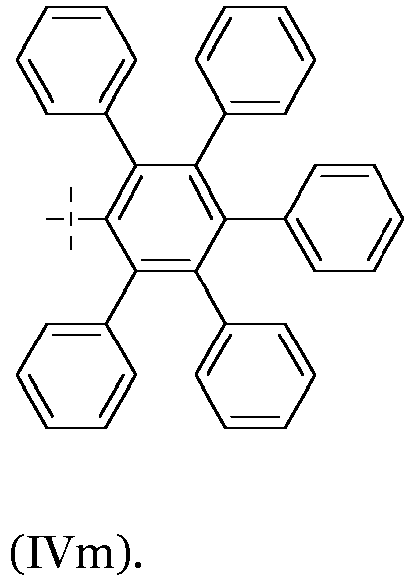
- Matériau semi-conducteur selon l'une quelconque des revendications précédentes, dans lequel le composé matriciel est sélectionné parmi l'un des composés a à g suivants


- Matériau semi-conducteur selon l'une quelconque des revendications précédentes, dans lequel le composé matriciel est un composé matriciel de transport d'électrons.
- Dispositif électronique comprenant une couche de semi-conducteur, ladite couche comprenant le matériau semi-conducteur selon l'une quelconque des revendications précédentes.
- Dispositif électronique selon la revendication 12, dans lequel le dispositif électronique est un dispositif électronique organique.
- Dispositif électronique selon l'une quelconque des revendications 12 et 13, dans lequel la couche de semi-conducteur organique est une couche de transport d'électrons.
- Procédé de préparation du matériau semi-conducteur selon l'une quelconque des revendications 1 à 11, le procédé comprenant les étapes(i) de co-évaporation du sel métallique divalent ou du complexe métallique divalent et du matériau matriciel ; et(ii) de co-dépôt du sel métallique divalent ou du complexe métallique divalent et du composé matriciel.
Priority Applications (5)
| Application Number | Priority Date | Filing Date | Title |
|---|---|---|---|
| EP17210292.3A EP3503242B1 (fr) | 2017-12-22 | 2017-12-22 | Matériau semi-conducteur, son procédé de préparation et dispositif électronique |
| PCT/EP2018/086243 WO2019122155A1 (fr) | 2017-12-22 | 2018-12-20 | Matériau semi-conducteur, son procédé de préparation et dispositif électronique |
| US16/956,412 US20210091311A1 (en) | 2017-12-22 | 2018-12-20 | Semiconducting Material, a Method for Preparing the Same and Electronic Device |
| KR1020207021090A KR20200103053A (ko) | 2017-12-22 | 2018-12-20 | 반도전성 물질, 이를 제조하는 방법 및 전자 디바이스 |
| CN201880082463.3A CN111566836B (zh) | 2017-12-22 | 2018-12-20 | 半导体材料、其制备方法以及电子器件 |
Applications Claiming Priority (1)
| Application Number | Priority Date | Filing Date | Title |
|---|---|---|---|
| EP17210292.3A EP3503242B1 (fr) | 2017-12-22 | 2017-12-22 | Matériau semi-conducteur, son procédé de préparation et dispositif électronique |
Publications (2)
| Publication Number | Publication Date |
|---|---|
| EP3503242A1 EP3503242A1 (fr) | 2019-06-26 |
| EP3503242B1 true EP3503242B1 (fr) | 2021-08-25 |
Family
ID=60915329
Family Applications (1)
| Application Number | Title | Priority Date | Filing Date |
|---|---|---|---|
| EP17210292.3A Active EP3503242B1 (fr) | 2017-12-22 | 2017-12-22 | Matériau semi-conducteur, son procédé de préparation et dispositif électronique |
Country Status (4)
| Country | Link |
|---|---|
| US (1) | US20210091311A1 (fr) |
| EP (1) | EP3503242B1 (fr) |
| KR (1) | KR20200103053A (fr) |
| WO (1) | WO2019122155A1 (fr) |
Families Citing this family (5)
| Publication number | Priority date | Publication date | Assignee | Title |
|---|---|---|---|---|
| EP3653619A1 (fr) * | 2018-11-16 | 2020-05-20 | Novaled GmbH | Composé, dispositif électronique organique le comprenant, dispositif d'affichage et dispositif d'éclairage le comprenant |
| DE102020103268B8 (de) * | 2020-02-10 | 2023-04-20 | Sichuan Knowledge Express Institute For Innovative Technologies Co., Ltd. | Ce(III)-Komplexe, Zusammensetzung aufweisend Ce(III)-Komplexe, optoelektronische Vorrichtung, Verfahren zu deren Herstellung, Verfahren zum Dublett-Harvesting und Verfahren für Hyperfluoreszenz mit sehr kurzer Abklingzeit |
| KR20220022178A (ko) | 2020-08-18 | 2022-02-25 | 주식회사 엘지에너지솔루션 | 이차전지 제조용 용접 장치 및 이를 이용한 용접 방법 |
| CN114512617A (zh) * | 2020-11-17 | 2022-05-17 | 京东方科技集团股份有限公司 | 一种发光器件、显示装置和发光器件的制作方法 |
| WO2023068824A1 (fr) * | 2021-10-20 | 2023-04-27 | 주식회사 엘지화학 | Nouveau composé et dispositif électroluminescent organique le comprenant |
Family Cites Families (7)
| Publication number | Priority date | Publication date | Assignee | Title |
|---|---|---|---|---|
| DE102007012794B3 (de) | 2007-03-16 | 2008-06-19 | Novaled Ag | Pyrido[3,2-h]chinazoline und/oder deren 5,6-Dihydroderivate, deren Herstellungsverfahren und diese enthaltendes dotiertes organisches Halbleitermaterial |
| EP2786433B1 (fr) | 2011-11-30 | 2018-08-01 | Novaled GmbH | Dispositif électronique organique |
| CN107434813B (zh) | 2011-11-30 | 2021-02-02 | 诺瓦尔德股份有限公司 | 显示器 |
| EP2722908A1 (fr) | 2012-10-17 | 2014-04-23 | Novaled AG | Diode électroluminescente organique phosphorescente et matières de transport de trous pour diodes électroluminescentes phosphorescentes |
| EP3171418A1 (fr) | 2015-11-23 | 2017-05-24 | Novaled GmbH | Couche semi-conductrice organique comprenant des composés d'oxyde de phosphine |
| EP3182478B1 (fr) | 2015-12-18 | 2018-11-28 | Novaled GmbH | Couche d'injection d'électrons pour une diode électroluminescente organique (oled) |
| EP3232490B1 (fr) | 2016-04-12 | 2021-03-17 | Novaled GmbH | Diode électroluminescente organique comprenant une couche semi-conductrice organique |
-
2017
- 2017-12-22 EP EP17210292.3A patent/EP3503242B1/fr active Active
-
2018
- 2018-12-20 US US16/956,412 patent/US20210091311A1/en not_active Abandoned
- 2018-12-20 WO PCT/EP2018/086243 patent/WO2019122155A1/fr active Application Filing
- 2018-12-20 KR KR1020207021090A patent/KR20200103053A/ko active IP Right Grant
Also Published As
| Publication number | Publication date |
|---|---|
| US20210091311A1 (en) | 2021-03-25 |
| KR20200103053A (ko) | 2020-09-01 |
| CN111566836A (zh) | 2020-08-21 |
| WO2019122155A1 (fr) | 2019-06-27 |
| EP3503242A1 (fr) | 2019-06-26 |
Similar Documents
| Publication | Publication Date | Title |
|---|---|---|
| EP3252837B1 (fr) | Diode électroluminescente organique comprenant une couche semi-conductrice organique | |
| US12029117B2 (en) | Organic electroluminescent device and a solid composition for use therein | |
| EP3503242B1 (fr) | Matériau semi-conducteur, son procédé de préparation et dispositif électronique | |
| EP3417495A1 (fr) | Couche de transport d'électrons comprenant un mélange de composés de matrice pour une diode électroluminescente organique (delo) | |
| EP3895226B1 (fr) | Dispositif électroluminescent organique et composé à utiliser en son sein | |
| EP3462516A1 (fr) | Dispositif électronique et son procédé de préparation | |
| KR102578661B1 (ko) | 유기 전계발광 디바이스 | |
| EP3759100A1 (fr) | Dispositif électronique organique, dispositifs d'affichage et d'éclairage le comprenant | |
| WO2019166269A1 (fr) | Dérivés de spiro-benzoanthracène-fluorène et leur utilisation dans des dispositifs électroniques organiques, des dispositifs d'affichage et des dispositifs d'éclairage | |
| EP3786159B1 (fr) | Composé triazine et couche semi-conductrice organique le comprenant | |
| US11527729B2 (en) | Electronic devices including semiconducting layers comprising at least one borate complex and methods for preparing the same | |
| US11524952B2 (en) | Compound and organic semiconducting layer, organic electronic device, display device and lighting device comprising the same | |
| EP3591725A1 (fr) | Dispositif électronique, son procédé de préparation et dispositif d'affichage le comprenant | |
| EP4312281A1 (fr) | Dispositif électronique organique et afficheur le comprenant | |
| EP3726599B1 (fr) | Composé, matériau semiconducteur organique le comprenant, dispositif électronique organique le comprenant, dispositif d'affichage et dispositif d'éclairage le comprenant | |
| EP3502116B1 (fr) | Composé et couche semi-conductrice organique le comprenant | |
| WO2023213705A1 (fr) | Diode électroluminescente organique et dispositif la comprenant | |
| WO2023213712A1 (fr) | Diode électroluminescente organique et dispositif la comprenant |
Legal Events
| Date | Code | Title | Description |
|---|---|---|---|
| PUAI | Public reference made under article 153(3) epc to a published international application that has entered the european phase |
Free format text: ORIGINAL CODE: 0009012 |
|
| STAA | Information on the status of an ep patent application or granted ep patent |
Free format text: STATUS: THE APPLICATION HAS BEEN PUBLISHED |
|
| AK | Designated contracting states |
Kind code of ref document: A1 Designated state(s): AL AT BE BG CH CY CZ DE DK EE ES FI FR GB GR HR HU IE IS IT LI LT LU LV MC MK MT NL NO PL PT RO RS SE SI SK SM TR |
|
| AX | Request for extension of the european patent |
Extension state: BA ME |
|
| RAP1 | Party data changed (applicant data changed or rights of an application transferred) |
Owner name: NOVALED GMBH |
|
| STAA | Information on the status of an ep patent application or granted ep patent |
Free format text: STATUS: REQUEST FOR EXAMINATION WAS MADE |
|
| 17P | Request for examination filed |
Effective date: 20191216 |
|
| RBV | Designated contracting states (corrected) |
Designated state(s): AL AT BE BG CH CY CZ DE DK EE ES FI FR GB GR HR HU IE IS IT LI LT LU LV MC MK MT NL NO PL PT RO RS SE SI SK SM TR |
|
| GRAP | Despatch of communication of intention to grant a patent |
Free format text: ORIGINAL CODE: EPIDOSNIGR1 |
|
| STAA | Information on the status of an ep patent application or granted ep patent |
Free format text: STATUS: GRANT OF PATENT IS INTENDED |
|
| GRAJ | Information related to disapproval of communication of intention to grant by the applicant or resumption of examination proceedings by the epo deleted |
Free format text: ORIGINAL CODE: EPIDOSDIGR1 |
|
| STAA | Information on the status of an ep patent application or granted ep patent |
Free format text: STATUS: REQUEST FOR EXAMINATION WAS MADE |
|
| INTG | Intention to grant announced |
Effective date: 20210305 |
|
| GRAP | Despatch of communication of intention to grant a patent |
Free format text: ORIGINAL CODE: EPIDOSNIGR1 |
|
| INTC | Intention to grant announced (deleted) | ||
| STAA | Information on the status of an ep patent application or granted ep patent |
Free format text: STATUS: GRANT OF PATENT IS INTENDED |
|
| INTG | Intention to grant announced |
Effective date: 20210422 |
|
| GRAS | Grant fee paid |
Free format text: ORIGINAL CODE: EPIDOSNIGR3 |
|
| GRAA | (expected) grant |
Free format text: ORIGINAL CODE: 0009210 |
|
| STAA | Information on the status of an ep patent application or granted ep patent |
Free format text: STATUS: THE PATENT HAS BEEN GRANTED |
|
| AK | Designated contracting states |
Kind code of ref document: B1 Designated state(s): AL AT BE BG CH CY CZ DE DK EE ES FI FR GB GR HR HU IE IS IT LI LT LU LV MC MK MT NL NO PL PT RO RS SE SI SK SM TR |
|
| REG | Reference to a national code |
Ref country code: CH Ref legal event code: EP |
|
| REG | Reference to a national code |
Ref country code: IE Ref legal event code: FG4D Ref country code: AT Ref legal event code: REF Ref document number: 1424710 Country of ref document: AT Kind code of ref document: T Effective date: 20210915 |
|
| REG | Reference to a national code |
Ref country code: DE Ref legal event code: R096 Ref document number: 602017044639 Country of ref document: DE |
|
| REG | Reference to a national code |
Ref country code: LT Ref legal event code: MG9D |
|
| REG | Reference to a national code |
Ref country code: NL Ref legal event code: MP Effective date: 20210825 |
|
| REG | Reference to a national code |
Ref country code: AT Ref legal event code: MK05 Ref document number: 1424710 Country of ref document: AT Kind code of ref document: T Effective date: 20210825 |
|
| PG25 | Lapsed in a contracting state [announced via postgrant information from national office to epo] |
Ref country code: RS Free format text: LAPSE BECAUSE OF FAILURE TO SUBMIT A TRANSLATION OF THE DESCRIPTION OR TO PAY THE FEE WITHIN THE PRESCRIBED TIME-LIMIT Effective date: 20210825 Ref country code: SE Free format text: LAPSE BECAUSE OF FAILURE TO SUBMIT A TRANSLATION OF THE DESCRIPTION OR TO PAY THE FEE WITHIN THE PRESCRIBED TIME-LIMIT Effective date: 20210825 Ref country code: HR Free format text: LAPSE BECAUSE OF FAILURE TO SUBMIT A TRANSLATION OF THE DESCRIPTION OR TO PAY THE FEE WITHIN THE PRESCRIBED TIME-LIMIT Effective date: 20210825 Ref country code: PT Free format text: LAPSE BECAUSE OF FAILURE TO SUBMIT A TRANSLATION OF THE DESCRIPTION OR TO PAY THE FEE WITHIN THE PRESCRIBED TIME-LIMIT Effective date: 20211227 Ref country code: NO Free format text: LAPSE BECAUSE OF FAILURE TO SUBMIT A TRANSLATION OF THE DESCRIPTION OR TO PAY THE FEE WITHIN THE PRESCRIBED TIME-LIMIT Effective date: 20211125 Ref country code: FI Free format text: LAPSE BECAUSE OF FAILURE TO SUBMIT A TRANSLATION OF THE DESCRIPTION OR TO PAY THE FEE WITHIN THE PRESCRIBED TIME-LIMIT Effective date: 20210825 Ref country code: ES Free format text: LAPSE BECAUSE OF FAILURE TO SUBMIT A TRANSLATION OF THE DESCRIPTION OR TO PAY THE FEE WITHIN THE PRESCRIBED TIME-LIMIT Effective date: 20210825 Ref country code: AT Free format text: LAPSE BECAUSE OF FAILURE TO SUBMIT A TRANSLATION OF THE DESCRIPTION OR TO PAY THE FEE WITHIN THE PRESCRIBED TIME-LIMIT Effective date: 20210825 Ref country code: BG Free format text: LAPSE BECAUSE OF FAILURE TO SUBMIT A TRANSLATION OF THE DESCRIPTION OR TO PAY THE FEE WITHIN THE PRESCRIBED TIME-LIMIT Effective date: 20211125 Ref country code: LT Free format text: LAPSE BECAUSE OF FAILURE TO SUBMIT A TRANSLATION OF THE DESCRIPTION OR TO PAY THE FEE WITHIN THE PRESCRIBED TIME-LIMIT Effective date: 20210825 |
|
| PG25 | Lapsed in a contracting state [announced via postgrant information from national office to epo] |
Ref country code: PL Free format text: LAPSE BECAUSE OF FAILURE TO SUBMIT A TRANSLATION OF THE DESCRIPTION OR TO PAY THE FEE WITHIN THE PRESCRIBED TIME-LIMIT Effective date: 20210825 Ref country code: LV Free format text: LAPSE BECAUSE OF FAILURE TO SUBMIT A TRANSLATION OF THE DESCRIPTION OR TO PAY THE FEE WITHIN THE PRESCRIBED TIME-LIMIT Effective date: 20210825 Ref country code: GR Free format text: LAPSE BECAUSE OF FAILURE TO SUBMIT A TRANSLATION OF THE DESCRIPTION OR TO PAY THE FEE WITHIN THE PRESCRIBED TIME-LIMIT Effective date: 20211126 |
|
| PG25 | Lapsed in a contracting state [announced via postgrant information from national office to epo] |
Ref country code: NL Free format text: LAPSE BECAUSE OF FAILURE TO SUBMIT A TRANSLATION OF THE DESCRIPTION OR TO PAY THE FEE WITHIN THE PRESCRIBED TIME-LIMIT Effective date: 20210825 |
|
| PG25 | Lapsed in a contracting state [announced via postgrant information from national office to epo] |
Ref country code: DK Free format text: LAPSE BECAUSE OF FAILURE TO SUBMIT A TRANSLATION OF THE DESCRIPTION OR TO PAY THE FEE WITHIN THE PRESCRIBED TIME-LIMIT Effective date: 20210825 |
|
| REG | Reference to a national code |
Ref country code: DE Ref legal event code: R097 Ref document number: 602017044639 Country of ref document: DE |
|
| PG25 | Lapsed in a contracting state [announced via postgrant information from national office to epo] |
Ref country code: SM Free format text: LAPSE BECAUSE OF FAILURE TO SUBMIT A TRANSLATION OF THE DESCRIPTION OR TO PAY THE FEE WITHIN THE PRESCRIBED TIME-LIMIT Effective date: 20210825 Ref country code: SK Free format text: LAPSE BECAUSE OF FAILURE TO SUBMIT A TRANSLATION OF THE DESCRIPTION OR TO PAY THE FEE WITHIN THE PRESCRIBED TIME-LIMIT Effective date: 20210825 Ref country code: RO Free format text: LAPSE BECAUSE OF FAILURE TO SUBMIT A TRANSLATION OF THE DESCRIPTION OR TO PAY THE FEE WITHIN THE PRESCRIBED TIME-LIMIT Effective date: 20210825 Ref country code: EE Free format text: LAPSE BECAUSE OF FAILURE TO SUBMIT A TRANSLATION OF THE DESCRIPTION OR TO PAY THE FEE WITHIN THE PRESCRIBED TIME-LIMIT Effective date: 20210825 Ref country code: CZ Free format text: LAPSE BECAUSE OF FAILURE TO SUBMIT A TRANSLATION OF THE DESCRIPTION OR TO PAY THE FEE WITHIN THE PRESCRIBED TIME-LIMIT Effective date: 20210825 Ref country code: AL Free format text: LAPSE BECAUSE OF FAILURE TO SUBMIT A TRANSLATION OF THE DESCRIPTION OR TO PAY THE FEE WITHIN THE PRESCRIBED TIME-LIMIT Effective date: 20210825 |
|
| PLBE | No opposition filed within time limit |
Free format text: ORIGINAL CODE: 0009261 |
|
| STAA | Information on the status of an ep patent application or granted ep patent |
Free format text: STATUS: NO OPPOSITION FILED WITHIN TIME LIMIT |
|
| PG25 | Lapsed in a contracting state [announced via postgrant information from national office to epo] |
Ref country code: MC Free format text: LAPSE BECAUSE OF FAILURE TO SUBMIT A TRANSLATION OF THE DESCRIPTION OR TO PAY THE FEE WITHIN THE PRESCRIBED TIME-LIMIT Effective date: 20210825 Ref country code: IT Free format text: LAPSE BECAUSE OF FAILURE TO SUBMIT A TRANSLATION OF THE DESCRIPTION OR TO PAY THE FEE WITHIN THE PRESCRIBED TIME-LIMIT Effective date: 20210825 |
|
| REG | Reference to a national code |
Ref country code: CH Ref legal event code: PL |
|
| 26N | No opposition filed |
Effective date: 20220527 |
|
| GBPC | Gb: european patent ceased through non-payment of renewal fee |
Effective date: 20211222 |
|
| PG25 | Lapsed in a contracting state [announced via postgrant information from national office to epo] |
Ref country code: SI Free format text: LAPSE BECAUSE OF FAILURE TO SUBMIT A TRANSLATION OF THE DESCRIPTION OR TO PAY THE FEE WITHIN THE PRESCRIBED TIME-LIMIT Effective date: 20210825 |
|
| REG | Reference to a national code |
Ref country code: BE Ref legal event code: MM Effective date: 20211231 |
|
| PG25 | Lapsed in a contracting state [announced via postgrant information from national office to epo] |
Ref country code: LU Free format text: LAPSE BECAUSE OF NON-PAYMENT OF DUE FEES Effective date: 20211222 Ref country code: IE Free format text: LAPSE BECAUSE OF NON-PAYMENT OF DUE FEES Effective date: 20211222 Ref country code: GB Free format text: LAPSE BECAUSE OF NON-PAYMENT OF DUE FEES Effective date: 20211222 |
|
| REG | Reference to a national code |
Ref country code: DE Ref legal event code: R079 Ref document number: 602017044639 Country of ref document: DE Free format text: PREVIOUS MAIN CLASS: H01L0051540000 Ipc: H10K0085000000 |
|
| PG25 | Lapsed in a contracting state [announced via postgrant information from national office to epo] |
Ref country code: FR Free format text: LAPSE BECAUSE OF NON-PAYMENT OF DUE FEES Effective date: 20211231 Ref country code: BE Free format text: LAPSE BECAUSE OF NON-PAYMENT OF DUE FEES Effective date: 20211231 |
|
| PG25 | Lapsed in a contracting state [announced via postgrant information from national office to epo] |
Ref country code: LI Free format text: LAPSE BECAUSE OF NON-PAYMENT OF DUE FEES Effective date: 20211231 Ref country code: CH Free format text: LAPSE BECAUSE OF NON-PAYMENT OF DUE FEES Effective date: 20211231 |
|
| P01 | Opt-out of the competence of the unified patent court (upc) registered |
Effective date: 20230515 |
|
| PG25 | Lapsed in a contracting state [announced via postgrant information from national office to epo] |
Ref country code: CY Free format text: LAPSE BECAUSE OF FAILURE TO SUBMIT A TRANSLATION OF THE DESCRIPTION OR TO PAY THE FEE WITHIN THE PRESCRIBED TIME-LIMIT Effective date: 20210825 |
|
| PG25 | Lapsed in a contracting state [announced via postgrant information from national office to epo] |
Ref country code: HU Free format text: LAPSE BECAUSE OF FAILURE TO SUBMIT A TRANSLATION OF THE DESCRIPTION OR TO PAY THE FEE WITHIN THE PRESCRIBED TIME-LIMIT; INVALID AB INITIO Effective date: 20171222 |
|
| PGFP | Annual fee paid to national office [announced via postgrant information from national office to epo] |
Ref country code: DE Payment date: 20231024 Year of fee payment: 7 |
|
| PG25 | Lapsed in a contracting state [announced via postgrant information from national office to epo] |
Ref country code: MK Free format text: LAPSE BECAUSE OF FAILURE TO SUBMIT A TRANSLATION OF THE DESCRIPTION OR TO PAY THE FEE WITHIN THE PRESCRIBED TIME-LIMIT Effective date: 20210825 |
|
| PG25 | Lapsed in a contracting state [announced via postgrant information from national office to epo] |
Ref country code: TR Free format text: LAPSE BECAUSE OF FAILURE TO SUBMIT A TRANSLATION OF THE DESCRIPTION OR TO PAY THE FEE WITHIN THE PRESCRIBED TIME-LIMIT Effective date: 20210825 |