EP3503240A1 - Organic semiconductor layer - Google Patents
Organic semiconductor layer Download PDFInfo
- Publication number
- EP3503240A1 EP3503240A1 EP17209694.3A EP17209694A EP3503240A1 EP 3503240 A1 EP3503240 A1 EP 3503240A1 EP 17209694 A EP17209694 A EP 17209694A EP 3503240 A1 EP3503240 A1 EP 3503240A1
- Authority
- EP
- European Patent Office
- Prior art keywords
- alkyl
- substituted
- alkoxy
- partially
- unsubstituted
- Prior art date
- Legal status (The legal status is an assumption and is not a legal conclusion. Google has not performed a legal analysis and makes no representation as to the accuracy of the status listed.)
- Granted
Links
- 0 *C1(*)c2ccc(Cc3nc(-c(cc4)cc(*5)c4-c4c5cccc4)nc([Al]I)n3)cc2-c2c1cccc2 Chemical compound *C1(*)c2ccc(Cc3nc(-c(cc4)cc(*5)c4-c4c5cccc4)nc([Al]I)n3)cc2-c2c1cccc2 0.000 description 7
- JVYDVOFHHHCSRG-UHFFFAOYSA-N Nc1cc(-c2cccc(C#N)c2)ccc1 Chemical compound Nc1cc(-c2cccc(C#N)c2)ccc1 JVYDVOFHHHCSRG-UHFFFAOYSA-N 0.000 description 1
- FMVREQADBPVLTH-UHFFFAOYSA-N Nc1cccc(-c(cc2)ccc2C#N)c1 Chemical compound Nc1cccc(-c(cc2)ccc2C#N)c1 FMVREQADBPVLTH-UHFFFAOYSA-N 0.000 description 1
- SCEKCBBNOVAFIJ-UHFFFAOYSA-N c1ccc(C(c2ccccc2-2)(c3c-2c(-c2nc(-c(cc4)ccc4-c4ccccc4)nc(-c4ccccc4)n2)ccc3)c2ccccc2)cc1 Chemical compound c1ccc(C(c2ccccc2-2)(c3c-2c(-c2nc(-c(cc4)ccc4-c4ccccc4)nc(-c4ccccc4)n2)ccc3)c2ccccc2)cc1 SCEKCBBNOVAFIJ-UHFFFAOYSA-N 0.000 description 1
- GPAOXWMGJRNDFD-UHFFFAOYSA-N c1ccc(C(c2ccccc2-2)(c3c-2c(-c2nc(-c4ccc(c5ccccc5[o]5)c5c4)nc(-c4ccccc4)n2)ccc3)c2ccccc2)cc1 Chemical compound c1ccc(C(c2ccccc2-2)(c3c-2c(-c2nc(-c4ccc(c5ccccc5[o]5)c5c4)nc(-c4ccccc4)n2)ccc3)c2ccccc2)cc1 GPAOXWMGJRNDFD-UHFFFAOYSA-N 0.000 description 1
Images


Classifications
-
- C—CHEMISTRY; METALLURGY
- C07—ORGANIC CHEMISTRY
- C07D—HETEROCYCLIC COMPOUNDS
- C07D405/00—Heterocyclic compounds containing both one or more hetero rings having oxygen atoms as the only ring hetero atoms, and one or more rings having nitrogen as the only ring hetero atom
- C07D405/02—Heterocyclic compounds containing both one or more hetero rings having oxygen atoms as the only ring hetero atoms, and one or more rings having nitrogen as the only ring hetero atom containing two hetero rings
- C07D405/04—Heterocyclic compounds containing both one or more hetero rings having oxygen atoms as the only ring hetero atoms, and one or more rings having nitrogen as the only ring hetero atom containing two hetero rings directly linked by a ring-member-to-ring-member bond
-
- C—CHEMISTRY; METALLURGY
- C07—ORGANIC CHEMISTRY
- C07D—HETEROCYCLIC COMPOUNDS
- C07D409/00—Heterocyclic compounds containing two or more hetero rings, at least one ring having sulfur atoms as the only ring hetero atoms
- C07D409/02—Heterocyclic compounds containing two or more hetero rings, at least one ring having sulfur atoms as the only ring hetero atoms containing two hetero rings
- C07D409/04—Heterocyclic compounds containing two or more hetero rings, at least one ring having sulfur atoms as the only ring hetero atoms containing two hetero rings directly linked by a ring-member-to-ring-member bond
-
- C—CHEMISTRY; METALLURGY
- C07—ORGANIC CHEMISTRY
- C07D—HETEROCYCLIC COMPOUNDS
- C07D421/00—Heterocyclic compounds containing two or more hetero rings, at least one ring having selenium, tellurium, or halogen atoms as ring hetero atoms
- C07D421/02—Heterocyclic compounds containing two or more hetero rings, at least one ring having selenium, tellurium, or halogen atoms as ring hetero atoms containing two hetero rings
- C07D421/04—Heterocyclic compounds containing two or more hetero rings, at least one ring having selenium, tellurium, or halogen atoms as ring hetero atoms containing two hetero rings directly linked by a ring-member-to-ring-member bond
-
- H—ELECTRICITY
- H10—SEMICONDUCTOR DEVICES; ELECTRIC SOLID-STATE DEVICES NOT OTHERWISE PROVIDED FOR
- H10K—ORGANIC ELECTRIC SOLID-STATE DEVICES
- H10K85/00—Organic materials used in the body or electrodes of devices covered by this subclass
- H10K85/60—Organic compounds having low molecular weight
- H10K85/649—Aromatic compounds comprising a hetero atom
- H10K85/654—Aromatic compounds comprising a hetero atom comprising only nitrogen as heteroatom
-
- H—ELECTRICITY
- H10—SEMICONDUCTOR DEVICES; ELECTRIC SOLID-STATE DEVICES NOT OTHERWISE PROVIDED FOR
- H10K—ORGANIC ELECTRIC SOLID-STATE DEVICES
- H10K85/00—Organic materials used in the body or electrodes of devices covered by this subclass
- H10K85/60—Organic compounds having low molecular weight
- H10K85/649—Aromatic compounds comprising a hetero atom
- H10K85/657—Polycyclic condensed heteroaromatic hydrocarbons
- H10K85/6574—Polycyclic condensed heteroaromatic hydrocarbons comprising only oxygen in the heteroaromatic polycondensed ring system, e.g. cumarine dyes
-
- C—CHEMISTRY; METALLURGY
- C07—ORGANIC CHEMISTRY
- C07D—HETEROCYCLIC COMPOUNDS
- C07D201/00—Preparation, separation, purification or stabilisation of unsubstituted lactams
-
- H—ELECTRICITY
- H10—SEMICONDUCTOR DEVICES; ELECTRIC SOLID-STATE DEVICES NOT OTHERWISE PROVIDED FOR
- H10K—ORGANIC ELECTRIC SOLID-STATE DEVICES
- H10K50/00—Organic light-emitting devices
- H10K50/10—OLEDs or polymer light-emitting diodes [PLED]
- H10K50/14—Carrier transporting layers
- H10K50/16—Electron transporting layers
- H10K50/165—Electron transporting layers comprising dopants
-
- Y—GENERAL TAGGING OF NEW TECHNOLOGICAL DEVELOPMENTS; GENERAL TAGGING OF CROSS-SECTIONAL TECHNOLOGIES SPANNING OVER SEVERAL SECTIONS OF THE IPC; TECHNICAL SUBJECTS COVERED BY FORMER USPC CROSS-REFERENCE ART COLLECTIONS [XRACs] AND DIGESTS
- Y02—TECHNOLOGIES OR APPLICATIONS FOR MITIGATION OR ADAPTATION AGAINST CLIMATE CHANGE
- Y02E—REDUCTION OF GREENHOUSE GAS [GHG] EMISSIONS, RELATED TO ENERGY GENERATION, TRANSMISSION OR DISTRIBUTION
- Y02E10/00—Energy generation through renewable energy sources
- Y02E10/50—Photovoltaic [PV] energy
- Y02E10/549—Organic PV cells
Definitions
- the present invention relates to an organic semiconductor layer, in particular to organic semiconductor layer comprising a compound substituted with bulky groups and a dopant, suitable for use as an organic semiconductor layer for electronic devices, and a method of manufacturing the same.
- Organic electronic devices such as organic light-emitting diodes OLEDs, which are self-emitting devices, have a wide viewing angle, excellent contrast, quick response, high brightness, excellent operating voltage characteristics, and color reproduction.
- a typical OLED comprises an anode, a hole transport layer HTL, an emission layer EML, an electron transport layer ETL, and a cathode, which are sequentially stacked on a substrate.
- the HTL, the EML, and the ETL are thin films formed from organic compounds.
- Performance of an organic light emitting diode may be affected by characteristics of the organic semiconductor layer, and among them, may be affected by characteristics of an organic material of the organic semiconductor layer.
- an organic semiconductor layer being capable of increasing electron mobility and simultaneously increasing electrochemical stability is needed so that the organic electronic device, such as an organic light emitting diode, may be applied to a large-size flat panel display.
- An aspect of the present invention provides an organic semiconductor layer comprising:
- Hetero atoms if not otherwise stated, can be individually selected from N, O, S, B, Si, P, Se, preferably from N, O and S and more preferred is N.
- H can represent hydrogen or deuterium.
- the organic semiconductor layer may comprise:
- the organic semiconductor layer may comprise:
- the organic semiconductor layer may comprise:
- the organic semiconductor layer may comprise:
- the organic semiconductor layer may comprise:
- the organic semiconductor layer may comprises:
- the organic semiconductor layer may comprise:
- X may be selected from O or S.
- R 1 , R 2 are independently selected from unsubstituted unsubstituted C 6 to C 24 aryl, or unsubstituted C 3 to C 24 heteroaryl, preferably R 1 , R 2 are independently selected from phenyl, biphenyl, terphenyl naphthyl, phenanthrenyl, pyridyl, quinolinyl, quinazolinyl, more preferred R 1 is selected from phenyl, biphenyl, terphenyl naphthyl, phenanthrenyl and R 2 is selected from pyridyl, quinolinyl, quinazolinyl.
- a high Tg may be achieved when R 1 , R 2 are selected in this range.
- Ar 1 may be selected from B1 to B6 and B16 to B23, preferably from B1 to B6, B16 to B17 and B19.
- Ar 1 may be selected from B1 to B6 and B16 to B23, preferably from B1 to B6, B16 to B17 and B19.
- the compound may be selected from D1 to D8:
- Ar 1 may be independently selected from structures C1 to C5: wherein R 3 , R 4 may be independently selected from C 1 to C 16 alkyl, C 1 to C 16 alkoxy, partially or perfluorinated C 1 to C 16 alkyl, partially or perfluorinated C 1 to C 16 alkoxy, partially or perdeuterated C 1 to C 16 alkyl, partially or perdeuterated C 1 to C 16 alkoxy, C 6 to C 18 aryl, C 3 to C 25 heteroaryl.
- R 3 , R 4 may be independently selected from C 1 to C 8 alkyl, C 1 to C 8 alkoxy, partially or perfluorinated C 1 to C 8 alkyl, partially or perfluorinated C 1 to C 8 alkoxy, partially or perdeuterated C 1 to C 8 alkyl, partially or perdeuterated C 1 to C 8 alkoxy, C 6 to C 12 aryl, C 3 to C 20 heteroaryl.
- R 3 , R 4 may be independently selected from C 1 to C 8 alkyl, partially or perdeuterated C 1 to C 8 alkyl, partially or perdeuterated C 1 to C 8 alkoxy, C 6 to C 12 aryl, C 3 to C 20 heteroaryl.
- R 3 , R 4 may be phenyl or C 1 to C4 alkyl, even more preferred phenyl or methyl.
- the organic semiconductor layer can be used as a layer for an organic electronic device.
- the organic electronic device can be an OLED or there like.
- the organic semiconductor layer comprising a compound of formula 1 and a dopant selected from an organic metal complex or metal halide have strong electron transport characteristics to increase charge mobility and/or stability and thereby to improve luminance efficiency, voltage characteristics, and/or lifetime characteristics.
- the organic semiconductor layer comprising a compound of formula 1 and a dopant selected from an organic metal complex or metal halide have high electron mobility and a low operating voltage.
- the organic semiconductor layer comprising a compound of formula 1 and a dopant selected from an organic metal complex or metal halide may be non-emissive.
- the term "essentially non-emissive" or “non-emitting” means that the contribution of the compound of formula 1 or layer comprising the compound of formula 1 and the dopant to the visible emission spectrum from the device is less than 10 %, preferably less than 5 %, further preferred less than 1 %, relative to the visible emission spectrum.
- the visible emission spectrum is an emission spectrum with a wavelength of about ⁇ 380 nm to about ⁇ 780 nm.
- the organic semiconductor layer comprising the compound of formula 1 is essentially non-emissive or non-emitting.
- the operating voltage also named U, is measured in Volt (V) at 10 milliAmpere per square centimeter (mA/cm2).
- the candela per Ampere efficiency also named cd/A efficiency, is measured in candela per ampere at 10 milliAmpere per square centimeter (mA/cm2).
- the external quantum efficiency also named EQE, is measured in percent (%).
- the color space is described by coordinates CIE-x and CIE-y (International Commission on Illumination 1931).
- CIE-x International Commission on Illumination 1931
- CIE-y International Commission on Illumination 1931
- a smaller CIE-y denotes a deeper blue color.
- the highest occupied molecular orbital, also named HOMO, and lowest unoccupied molecular orbital, also named LUMO, are measured in electron volt (eV).
- the rate onset temperature is measured in °C and describes the VTE source temperature at which measurable evaporation of a compound commences at a pressure of less than 10 -5 mbar.
- OLED organic light emitting diode
- organic light emitting device organic optoelectronic device
- organic light-emitting diode organic light-emitting diode
- transition metal means and comprises any element in the d-block of the periodic table, which comprises groups 3 to 12 elements on the periodic table.
- group III to VI metal means and comprises any metal in groups III to VI of the periodic table.
- weight percent As used herein, “weight percent”, “wt.-%”, “percent by weight”, “% by weight”, and variations thereof refer to a composition, component, substance or agent as the weight of that composition, component, substance or agent of the respective electron transport layer divided by the total weight of the composition thereof and multiplied by 100. It is understood that the total weight percent amount of all components, substances or agents of the respective electron transport layer are selected such that it does not exceed 100 wt.-%.
- volume percent As used herein, “volume percent”, “vol.-%”, “percent by volume”, “% by volume”, and variations thereof refer to an elemental metal, a composition, component, substance or agent as the volume of that elemental metal, component, substance or agent of the respective electron transport layer divided by the total volume of the respective electron transport layer thereof and multiplied by 100. It is understood that the total volume percent amount of all elemental metal, components, substances or agents of the respective cathode electrode layer are selected such that it does not exceed 100 vol.-%.
- the anode electrode and cathode electrode may be described as anode electrode / cathode electrode or anode electrode / cathode electrode or anode electrode layer / cathode electrode layer.
- an organic optoelectronic device comprises an anode layer and a cathode layer facing each other and at least one organic semiconductor layer between the anode layer and the cathode layer, wherein the organic semiconductor layer comprises or consists of the compound of formula 1.
- a display device comprising the organic electronic device, which can be an organic optoelectronic device, is provided.
- an "alkyl group” may refer to an aliphatic hydrocarbon group.
- the alkyl group may refer to "a saturated alkyl group” without any double bond or triple bond.
- the alkyl group may be a linear, cyclic or branched alkyl group.
- the alkyl group may be a C 1 to C 16 alkyl group, or preferably a C 1 to C 12 alkyl group. More specifically, the alkyl group may be a C 1 to C 14 alkyl group, or preferably a C 1 to C 10 alkyl group or a C 1 to C 6 alkyl group.
- a C 1 to C 4 alkyl group comprises 1 to 4 carbons in alkyl chain, and may be selected from methyl, ethyl, propyl, iso-propyl, n-butyl, iso-butyl, sec-butyl, and t-butyl.
- alkyl group may be a methyl group, an ethyl group, a propyl group, an isopropyl group, a butyl group, an isobutyl group, a tert-butyl group, a pentyl group, a hexyl group, a cyclopropyl group, a cyclobutyl group, a cyclopentyl group, a cyclohexyl group, and the like.
- arylene group may refer to a group comprising at least one hydrocarbon aromatic moiety, and all the elements of the hydrocarbon aromatic moiety may have p-orbitals which form conjugation, for example a phenyl group, a naphthyl group, an anthracenyl group, a phenanthrenyl group, a pyrenyl group, a fluorenyl group and the like.
- heteroarylene may refer to aromatic heterocycles with at least one heteroatom, and all the elements of the hydrocarbon heteroaromatic moiety may have p-orbitals which form conjugation.
- hetero-fluorene ring refers to a dibenzo[d,d]furanyl, dibenzo[b,d]thiophenyl or dibenzo[b,d]selenophenyl group.
- the heteroatom may be selected from N, O, S, B, Si, P, Se, preferably from N, O and S.
- a heteroarylene ring may comprise at least 1 to 3 heteroatoms.
- a heteroarylene ring may comprise at least 1 to 3 heteroatoms individually selected from N, S and/or O.
- At least one additional heteroaryl/ene ring may comprise at least 1 to 3 N-atoms, or at least 1 to 2-N atoms or at least one N-atom.
- the compound according to formula 1 may comprise:
- the compound of formula 1 comprises at least 2 to 7, preferably 2 to 5, or 2 to 3 hetero aromatic rings.
- the compound of formula 1 comprises at least 2 to 7, preferably 2 to 5, or 2 to 3 hetero aromatic rings, wherein at least one of the aromatic rings is a five member hetero aromatic ring.
- the compound of formula 1 comprises at least 3 to 7, preferably 3 to 6, or 3 to 5 hetero aromatic rings, wherein at least two of the hetero aromatic rings are five member hetero-aromatic-rings.
- the compound according to formula 1 may comprise at least 6 to 12 non-hetero aromatic rings and 2 to 3 hetero aromatic rings.
- the compound according to formula 1 may comprise at least 7 to 12 non-hetero aromatic rings and 2 to 5 hetero aromatic rings.
- the compound according to formula 1 may comprise at least 7 to 11 non-hetero aromatic rings and 2 to 3 hetero aromatic rings.
- the melting point (mp) is determined as peak temperatures from the DSC curves of the above TGA-DSC measurement or from separate DSC measurements (Mettler Toledo DSC822e, heating of samples from room temperature to completeness of melting with heating rate 10 K/min under a stream of pure nitrogen. Sample amounts of 4 to 6 mg are placed in a 40 ⁇ L Mettler Toledo aluminum pan with lid, a ⁇ 1 mm hole is pierced into the lid).
- the compound of formula 1 may have a melting point of about ⁇ 250° C and about ⁇ 380° C, preferably about ⁇ 260° C and about ⁇ 370° C, further preferred about ⁇ 270° C and about ⁇ 360° C, in addition preferred about ⁇ 275° C and about ⁇ 350° C, also preferred about ⁇ 280° C and about ⁇ 340° C, likewise preferred about ⁇ 285° C and about ⁇ 330° C and more preferred about ⁇ 290° C and about ⁇ 310° C.
- the glass transition temperature is measured under nitrogen and using a heating rate of 10 K per min in a Mettler Toledo DSC 822e differential scanning calorimeter as described in DIN EN ISO 11357, published in March 2010.
- the compound of formula 1 may have a glass transition temperature Tg of about ⁇ 120° C and about ⁇ 380° C, preferably about ⁇ 130° C and about ⁇ 350° C, further preferred about ⁇ 140° C and about ⁇ 320° C, in addition preferred about ⁇ 140° C and about ⁇ 200° C and also preferred about ⁇ 140° C and about ⁇ 180° C.
- the rate onset temperature is determined by loading 100 mg compound into a VTE source.
- the VTE source is heated at a constant rate of 15 K/min at a pressure of less than 10 -5 mbar and the temperature inside the source measured with a thermocouple. Evaporation of the compound is detected with a QCM detector which detects deposition of the compound on the quartz crystal of the detector. The deposition rate on the quartz crystal is measured in ⁇ ngstrom per second. To determine the rate onset temperature, the deposition rate is plotted against the VTE source temperature. The rate onset is the temperature at which noticeable deposition on the QCM detector occurs. For accurate results, the VTE source is heated and cooled three time and only results from the second and third run are used to determine the rate onset temperature.
- the rate onset temperature may be in the range of 200 to 255 °C. If the rate onset temperature is below 200 °C the evaporation may be too rapid and therefore difficult to control. If the rate onset temperature is above 255 °C the evaporation rate may be too low which may result in low takt time and decomposition of the organic compound in VTE source may occur due to prolonged exposure to elevated temperatures.
- the rate onset temperature is an indirect measure of the volatility of a compound. The higher the rate onset temperature the lower is the volatility of a compound.
- the compound of formula 1 may have a rate onset temperature T RO of about ⁇ 200° C and about ⁇ 350° C, preferably about ⁇ 220° C and about ⁇ 350° C, further preferred about ⁇ 240° C and about ⁇ 320° C, in addition preferred about ⁇ 240° C and about ⁇ 300° C and more preferred about ⁇ 240° C and about ⁇ 280° C.
- the dipole moment is determined by a semi-empirical molecular orbital method.
- the geometries of the molecular structures are optimized using the hybrid functional B3LYP with the 6-31G* basis set in the gas phase as implemented in the program package TURBOMOLE V6.5. If more than one conformation is viable, the conformation with the lowest total energy is selected to determine the bond lengths of the molecules.
- the compounds according to formula 1 may have a dipole moment (Debye) in the range from about ⁇ 0.25 to about ⁇ 1.50, preferably from about ⁇ 0.28 to about ⁇ 1.00, further preferred from about ⁇ 0.30 to about ⁇ 0.70, also preferred from about ⁇ 0.32 to about ⁇ 0.60.
- Debye dipole moment
- the HOMO and LUMO are calculated with the program package TURBOMOLE V6.5.
- the optimized geometries and the HOMO and LUMO energy levels of the molecular structures are determined by applying the hybrid functional B3LYP with a 6-31G* basis set in the gas phase. If more than one conformation is viable, the conformation with the lowest total energy is selected.
- the compounds according to formula 1 may have a LUMO energy level (eV) in the range from about - 2.10 eV to about - 1.90 eV, preferably from about - 1.99 eV to about - 1.91 eV, further preferred from about - 1.98 eV to about - 1.92 eV, also preferred from about - 1.97 eV to about - 1.93 eV.
- eV LUMO energy level
- the isosurfaces of the orbitals are plotted in the graphical user interface TMolex Version 3.3.
- the 3D data for this property is generated using a coarse grid and a value of 0.03 was chosen to plot the positive and negative iso-densities of the isosurfaces.
- the compounds of formula 1 and the inventive organic electronic devices solve the problem underlying the present invention by being superior over the organic electroluminescent devices and compounds known in the art, in particular with respect to cd/A efficiency, also referred to as current efficiency and to lifetime.
- cd/A efficiency also referred to as current efficiency and to lifetime.
- the operating voltage is kept at a similar or even improved level which is important for reducing power consumption and increasing battery life, for example of a mobile display device.
- High cd/A efficiency is important for high efficiency and thereby increased battery life of a mobile device, for example a mobile display device. Long lifetime at high current density is important for the longevity of a device which is run at high brightness.
- the calculated LUMO level of compounds of formula 1 is significantly more negative than the LUMO of the state of the art.
- a more negative LUMO may be beneficial for improved electron transfer from the cathode to the emission layer.
- more efficient electron transfer from neighbouring molecules and/or the cathode and/or improved stability of the molecule itself may be achieved when the LUMO is delocalized over the atoms in the triazine group and over the majority of atoms in the dibenzo[d,d]furanyl, dibenzo[b,d]thiophenyl or dibenzo[b,d]selenophenyl group and in the triazinyl group.
- the inventors have surprisingly found that particular good performance can be achieved when using the organic electroluminescent device as a fluorescent blue device.
- organic optoelectronic device having high efficiency and/or long lifetime may be realized.
- a material for the anode may be a metal or a metal oxide, or an organic material, preferably a material with work function above about 4.8 eV, more preferably above about 5.1 eV, most preferably above about 5.3 eV.
- Preferred metals are noble metals like Pt, Au or Ag, preferred metal oxides are transparent metal oxides like ITO or IZO which may be advantageously used in bottom-emitting OLEDs having a reflective cathode.
- the anode may have a thickness from about 50 nm to about 100 nm, whereas semitransparent metal anodes may be as thin as from about 5 nm to about 15 nm, and non-transparent metal anodes may have a thickness from about 15 nm to about 150nm.
- HIL Hole injection layer
- the hole injection layer may improve interface properties between the anode and an organic material used for the hole transport layer, and is applied on a non-planarized anode and thus may planarize the surface of the anode.
- the hole injection layer may include a material having a median value of the energy level of its highest occupied molecular orbital (HOMO) between the work function of the anode material and the energy level of the HOMO of the hole transport layer, in order to adjust a difference between the work function of the anode and the energy level of the HOMO of the hole transport layer.
- HOMO highest occupied molecular orbital
- the hole injection layer may be formed on the anode by any of a variety of methods, for example, vacuum deposition, spin coating, casting, Langmuir-Blodgett (LB) method, or the like.
- vacuum deposition conditions may vary depending on the material that is used to form the hole injection layer, and the desired structure and thermal properties of the hole injection layer to be formed and for example, vacuum deposition may be performed at a temperature of about 100 °C to about 500 °C, a pressure of about 10 -6 Pa to about 10 -1 Pa, and a deposition rate of about 0.1 to about 10 nm/sec, but the deposition conditions are not limited thereto.
- the coating conditions may vary depending on the material that is used to form the hole injection layer, and the desired structure and thermal properties of the hole injection layer to be formed.
- the coating rate may be in the range of about 2000 rpm to about 5000 rpm
- a temperature at which heat treatment is performed to remove a solvent after coating may be in a range of about 80 °C to about 200 °C, but the coating conditions are not limited thereto.
- the hole injection layer may further comprise a p-dopant to improve conductivity and/or hole injection from the anode.
- the p-dopant may be homogeneously dispersed in the hole injection layer.
- the p-dopant may be present in the hole injection layer in a higher concentration closer to the anode and in a lower concentration closer to the cathode.
- the p-dopant may be one of a quinone derivative or a radialene compound but not limited thereto.
- the p-dopant are quinone derivatives such as tetracyanoquinonedimethane (TCNQ), 2,3,5,6-tetrafluoro-tetracyano-1,4-benzoquinonedimethane (F4-TCNQ), 4,4',4"-((1E,1'E,1"E)-cyclopropane-1,2,3-triylidenetris(cyanomethanylylidene))-tris(2,3,5,6-tetrafluorobenzonitrile).
- quinone derivatives such as tetracyanoquinonedimethane (TCNQ), 2,3,5,6-tetrafluoro-tetracyano-1,4-benzoquinonedimethane (F4-TCNQ), 4,4',4"-((1E,1'E,
- an organic electronic device comrising an organic semiconductor layer that comprises a compound of formula 1 and a dopant selected from an organic metal complex or metal halide may additional comprise a layer comprising a radialene compound and/or a quinodimethane compound.
- the radialene compound and/or the quinodimethane compound may be substituted with one or more halogen atoms and/or with one or more electron withdrawing groups.
- Electron withdrawing groups can be selected from nitrile groups, halogenated alkyl groups, alternatively from perhalogenated alkyl groups, alternatively from perfluorinated alkyl groups.
- Other examples of electron withdrawing groups may be acyl, sulfonyl groups or phosphoryl groups.
- acyl groups, sulfonyl groups and/or phosphoryl groups may comprise halogenated and/or perhalogenated hydrocarbyl.
- the perhalogenated hydrocarbyl may be a perfluorinated hydrocarbyl.
- Examples of a perfluorinated hydrocarbyl can be perfluormethyl, perfluorethyl, perfluorpropyl, perfluorisopropyl, perfluorobutyl, perfluorophenyl, perfluorotolyl; examples of sulfonyl groups comprising a halogenated hydrocarbyl may be trifluoromethylsulfonyl, pentafluoroethylsulfonyl, pentafluorophenylsulfonyl, heptafluoropropylsufonyl, nonafluorobutylsulfonyl, and like.
- the radialene and/or the quinodimethane compound may be comprised in a hole injection, hole transporting and/or a hole generation layer.
- the radialene compound may have formula (XX) and/or the quinodimethane compound may have formula (XXIa) or (XXIb): wherein R 1 ", R 2 ", R 3 ", R 4 ", R 5 “, R 6 , R 7 , R 8 , R 11 , R 12 , R 15 , R 16 , R 20 , R 21 are independently selected from an electron withdrawing groups and R 9 , R 10 , R 13 , R 14 , R 17 , R 18 , R 19 , R 22 , R 23 and R 24 are independently selected from H, halogen and electron withdrawing groups. Electron withdrawing group/s that can be suitable used are above mentioned.
- HTL Hole transport layer
- Conditions for forming the hole transport layer and the electron blocking layer may be defined based on the above-described formation conditions for the hole injection layer.
- a thickness of the hole transport part of the charge transport region may be from about 10 nm to about 1000 nm, for example, about 10 nm to about 100 nm.
- a thickness of the hole injection layer may be from about 10 nm to about 1000 nm, for example about 10 nm to about 100 nm and a thickness of the hole transport layer may be from about 5 nm to about 200 nm, for example about 10 nm to about 150 nm.
- Hole transport matrix materials used in the hole transport region are not particularly limited. Preferred are covalent compounds comprising a conjugated system of at least 6 delocalized electrons, preferably organic compounds comprising at least one aromatic ring, more preferably organic compounds comprising at least two aromatic rings, even more preferably organic compounds comprising at least three aromatic rings, most preferably organic compounds comprising at least four aromatic rings.
- Typical examples of hole transport matrix materials which are widely used in hole transport layers are polycyclic aromatic hydrocarbons, triarylene amine compounds and heterocyclic aromatic compounds. Suitable ranges of frontier orbital energy levels of hole transport matrices useful in various layer of the hole transport region are well-known.
- the preferred values may be in the range 0.0 - 1.0 V, more preferably in the range 0.2 - 0.7 V, even more preferably in the range 0.3 - 0.5 V.
- the hole transport part of the charge transport region may further include a buffer layer.
- Buffer layer that can be suitable used are disclosed in US 6 140 763 , US 6 614 176 and in US2016/248022 .
- the buffer layer may compensate for an optical resonance distance of light according to a wavelength of the light emitted from the EML, and thus may increase efficiency.
- Emission layer Emission layer
- the emission layer may be formed on the hole transport region by using vacuum deposition, spin coating, casting, LB method, or the like.
- the conditions for deposition and coating may be similar to those for the formation of the hole injection layer, though the conditions for the deposition and coating may vary depending on the material that is used to form the emission layer.
- the emission layer may include an emitter host (EML host) and an emitter dopant (further only emitter).
- a thickness of the emission layer may be about 100 ⁇ to about 1000 ⁇ , for example about 200 ⁇ to about 600 ⁇ . When the thickness of the emission layer is within these ranges, the emission layer may have improved emission characteristics without a substantial increase in operating voltage.
- the emission layer comprises compound of formula 1 as emitter host.
- the emitter host compound has at least three aromatic rings, which are independently selected from carbocyclic rings and heterocyclic rings.
- Arm and Ar 112 may be each independently a substituted or unsubstituted C 6 -C 60 arylene group;
- Ar 113 to Ar 116 may be each independently a substituted or unsubstituted C 1 -C 10 alkyl group or a substituted or unsubstituted C 6 -C 60 arylene group;
- g, h, i, and j may be each independently an integer from 0 to 4.
- Ar 111 and Ar 112 in formula 400 may be each independently one of a phenylene group, a naphthalene group, a phenanthrenylene group, or a pyrenylene group; or a phenylene group, a naphthalene group, a phenanthrenylene group, a fluorenyl group, or a pyrenylene group, each substituted with at least one of a phenyl group, a naphthyl group, or an anthryl group.
- g, h, i, and j may be each independently an integer of 0, 1, or 2.
- Ar 113 to Ar 116 may be each independently one of
- X is selected form an oxygen atom and a sulfur atom, but embodiments of the invention are not limited thereto.
- any one of R 11 to R 14 is used for bonding to Arm.
- R 11 to R 14 that are not used for bonding to Arm and R 15 to R 20 are the same as R 1 to R 8 .
- any one of R 21 to R 24 is used for bonding to Arm.
- R 21 to R 24 that are not used for bonding to Ar 111 and R 25 to R 30 are the same as R 1 to R 8 .
- the EML host comprises between one and three heteroatoms selected from the group consisting of N, O or S. More preferred the EML host comprises one heteroatom selected from S or O.
- the dopant is mixed in a small amount to cause light emission, and may be generally a material such as a metal complex that emits light by multiple excitation into a triplet or more.
- the dopant may be, for example an inorganic, organic, or organic/inorganic compound, and one or more kinds thereof may be used.
- the emitter may be a red, green, or blue emitter.
- the dopant may be a fluorescent dopant, for example ter-fluorene, the structures are shown below.
- a fluorescent dopant for example ter-fluorene
- DPAVBI 4.4'-bis(4-diphenyl amiostyryl)biphenyl
- TBPe 2,5,8,11-tetra-tert-butyl perylene
- Compound 8 are examples of fluorescent blue dopants.
- the dopant may be a phosphorescent dopant, and examples of the phosphorescent dopant may be an organic metal compound comprising Ir, Pt, Os, Ti, Zr, Hf, Eu, Tb, Tm, Fe, Co, Ni, Ru, Rh, Pd, or a combination thereof.
- the phosphorescent dopant may be, for example a compound represented by formula Z, but is not limited thereto: J 2 MX (Z).
- M is a metal
- J and X are the same or different, and are a ligand to form a complex compound with M.
- the M may be, for example Ir, Pt, Os, Ti, Zr, Hf, Eu, Tb, Tm, Fe, Co, Ni, Ru, Rh, Pd or a combination thereof, and the J and X may be, for example a bidendate ligand.
- One or more emission layers may be arranged between the anode and the cathode. To increase overall performance, two or more emission layers may be present.
- a charge generation layer (also named CGL) may be arranged between the first and the second emission layer, and second and third emission layer, if present.
- the CGL comprises a n-type charge generation layer (also named n-CGL or electron generation layer) and a p-type charge generation layer (also named p-CGL or hole generation layer).
- An interlayer may be arranged between the n-type CGL and the p-type CGL.
- the n-type CGL may comprise a compound of formula 1.
- the n-type CGL further comprises a metal, metal salt or organic metal complex, preferably a metal.
- the metal may be selected from an alkali, alkaline earth or rare earth metal.
- the p-type CGL may comprise a dipyrazino[2,3-f:2',3'-h]quinoxaline, a quinone compound or a radialene compound, preferably dipyrazino[2,3-f:2',3'-h]quinoxaline-2,3,6,7,10,11-hexacarbonitrile or a compound or formula (XX) and/or a compound of formula (XXIa) or (XXIb).
- Electron transport layer ETL
- the organic semiconductor layer that comprises compound of formula 1 is an electron transport layer.
- the electron transport layer may consist of compound of formula 1.
- an organic light emitting diode comprises at least one electron transport layer, and in this case, the electron transport layer comprises compound of formula 1, or preferably of at least one compound of formulae D1 to D8.
- the organic electronic device comprises an electron transport region of a stack of organic layers formed by two or more electron transport layers, wherein at least one electron transport layer comprises compound of formula 1 and a dopant selected from an organic metal complex or metal halide.
- the electron transport layer may include one or two or more different electron transport compounds.
- a first and a second electron transport layers comprise compound of formula 1 and a dopant selected from an organic metal complex or metal halide, wherein the compound of formula 1 is not selected the same.
- the thickness of the first electron transport layer may be from about 0.5 nm to about 100 nm, for example about 2 nm to about 40 nm. When the thickness of the first electron transport layer is within these ranges, the first electron transport layer may have improved electron transport ability without a substantial increase in operating voltage.
- a thickness of an optional second electron transport layer may be about 1 nm to about 100 nm, for example about 2 nm to about 20 nm. When the thickness of the electron transport layer is within these ranges, the electron transport layer may have satisfactory electron transporting ability without a substantial increase in operating voltage.
- the dopant of the electron transport layer may be a monovalent or divalent metal halide or an organic monovalent or divalent metal complex, preferably an alkali halide and/or alkali organic complex.
- the first and second electron transport layers comprise compound of formula 1, wherein the second electron transport layer further comprises the dopant selected from an organic metal complex or metal halide, preferably an alkali halide and/or alkali organic complex.
- Alkali halides that can be suitable used as the dopant are the family of inorganic compounds with the chemical formula MX, where M is an alkali metal and X is a halogen.
- M can be selected from Li, Na, Potassium, Rubidium and Cesium.
- X can be selected from F, Cl, Br and J.
- a lithium halide may be preferred.
- the lithium halide can be selected from the group comprising LiF, LiCl, LiBr and LiJ. However, most preferred is LiF.
- the alkali halide is essentially non-emissive or non-emissive.
- the alkali organic complex that can be suitable used as the dopant as organic metal complex comprises an alkali metal and at least one organic ligand.
- the alkali metal is preferably selected from lithium.
- the organic ligand of the lithium organic complex is a quinolate, a borate, a phenolate, a pyridinolate or a Schiff base ligand;
- the organic ligand of the alkali organic complex preferably of a lithium organic complex
- Quinolates that can be suitable used are disclosed in WO 2013079217 A1 and incorporated by reference.
- the organic ligand of the lithium organic complex can be a borate based organic ligand,
- the lithium organic complex is a lithium tetra(1H-pyrazol-1-yl)borate.
- Borate based organic ligands that can be suitable used are disclosed in WO 2013079676 A1 and incorporated by reference.
- the organic ligand of the lithium organic complex can be a phenolate ligand,
- the lithium organic complex is a lithium 2-(diphenylphosphoryl)phenolate.
- Phenolate ligands that can be suitable used are disclosed in WO 2013079678 A1 and incorporated by reference.
- phenolate ligands can be selected from the group of pyridinolate, preferably 2-(diphenylphosphoryl)pyridin-3-olate. Pyridine phenolate ligands that can be suitable used are disclosed in JP 2008195623 and incorporated by reference.
- phenolate ligands can be selected from the group of imidazol phenolates, preferably 2-(1-phenyl-1H-benzo[d]imidazol-2-yl)phenolate. Imidazol phenolate ligands that can be suitable used are disclosed in JP 2001291593 and incorporated by reference.
- phenolate ligands can be selected from the group of oxazol phenolates, preferably 2-(benzo[d]oxazol-2-yl)phenolate.
- Oxazol phenolate ligands that can be suitable used are disclosed in US 20030165711 and incorporated by reference.
- the alkali organic complex may be essentially non-emissive.
- Electron injection layer (EIL)
- the organic electroluminescent device may further comprise an electron injection layer between the electron transport layer (first-ETL) and the cathode.
- the electron injection layer may facilitate injection of electrons from the cathode.
- the electron injection layer comprises:
- the electron injection layer may include at least one selected from LiF, NaCl, CsF, Li 2 O, and BaO.
- a thickness of the EIL may be from about 0.1 nm to about 10 nm, or about 0.3 nm to about 9 nm. When the thickness of the electron injection layer is within these ranges, the electron injection layer may have satisfactory electron injection ability without a substantial increase in operating voltage.
- the electron injection layer may comprise a compound of formula 1.
- a material for the cathode may be a metal, an alloy, or an electrically conductive compound that have a low work function, or a combination thereof.
- Specific examples of the material for the cathode may be lithium (Li), magnesium (Mg), aluminum (Al), aluminum-lithium (Al-Li), calcium (Ca), magnesium-indium (Mg-In), magnesium-silver (Mg-Ag), silver (Ag) etc.
- the cathode may be formed as a light-transmissive electrode from, for example, indium tin oxide (ITO), indium zinc oxide (IZO) or silver (Ag).
- the cathode may have a thickness from about 50 nm to about 100 nm, whereas semitransparent metal cathodes may be as thin as from about 5 nm to about 15 nm.
- a substrate may be further disposed under the anode or on the cathode.
- the substrate may be a substrate that is used in a general organic light emitting diode and may be a glass substrate or a transparent plastic substrate with strong mechanical strength, thermal stability, transparency, surface smoothness, ease of handling, and water resistance.
- first element when a first element is referred to as being formed or disposed "on" a second element, the first element can be disposed directly on the second element, or one or more other elements may be disposed there between.
- first element when referred to as being formed or disposed "directly on” a second element, no other elements are disposed there between.
- contacting sandwiched refers to an arrangement of three layers whereby the layer in the middle is in direct contact with the two adjacent layers.
- the organic light emitting diodes according to an embodiment of the present invention may include a hole transport region; an emission layer; and a first electron transport layer comprising a compound according to formula 1 and a dopant selected from an organic metal complex or metal halide.
- FIG. 1 is a schematic sectional view of an organic light-emitting diode 100, according to an exemplary embodiment of the present invention.
- the OLED 100 comprises an emission layer 150, an electron transport layer (ETL) 161 comprising compound of formula 1 and a dopant selected from an organic metal complex or metal halide, and an electron injection layer 180, whereby the first electron transport layer 161 is disposed directly on the emission layer 150 and the electron injection layer 180 is disposed directly on the first electron transport layer 161.
- ETL electron transport layer
- FIG. 2 is a schematic sectional view of an organic light-emitting diode 100, according to an exemplary embodiment of the present invention.
- the OLED 100 comprises an emission layer 150 and an electron transport layer stack (ETL) 160 comprising a first electron transport layer 161, and a second electron transport layer 162 comprising a compound of formula 1 and a dopant selected from an organic metal complex or metal halide, whereby the second electron transport layer 162 is disposed directly on the first electron transport layer 161.
- ETL electron transport layer stack
- FIG. 3 is a schematic sectional view of an organic light-emitting diode 100, according to an exemplary embodiment of the present invention.
- the OLED 100 comprises an emission layer 150 and an electron transport layer stack (ETL) 160 comprising a first electron transport layer 161, a second electron transport layer 162, and a third electron transport layer 163, whereby the second electron transport layer 162 is disposed directly on the first electron transport layer 161 and the third electron transport layer 163 is disposed directly on the first electron transport layer 162.
- the first and/or the second and/or the third electron transport layer comprise a compound of formula 1 and a dopant selected from an organic metal complex or metal halide.
- FIG. 4 is a schematic sectional view of an organic light-emitting diode 100, according to an exemplary embodiment of the present invention.
- the OLED 100 comprises a substrate 110, a first anode electrode 120, a hole injection layer (HIL) 130, a hole transport layer (HTL) 140, an emission layer (EML) 150, one first electron transport layer (ETL) 161, an electron injection layer (EIL) 180, and a cathode electrode 190.
- the first electron transport layer (ETL) 161 comprises compound of formula 1 and a dopant selected from an organic metal complex or metal halide.
- the electron transport layer (ETL) 161 is formed directly on the EML 150.
- FIG. 5 is a schematic sectional view of an organic light-emitting diode 100, according to an exemplary embodiment of the present invention.
- the OLED 100 comprises a substrate 110, a first anode electrode 120, a hole injection layer (HIL) 130, a hole transport layer (HTL) 140, an emission layer (EML) 150, an electron transport layer stack (ETL) 160, an electron injection layer (EIL) 180, and a cathode electrode 190.
- the electron transport layer (ETL) 160 comprises a first electron transport layer 161 and a second electron transport layer 162, wherein the first electron transport layer is arranged near to the anode (120) and the second electron transport layer is arranged near to the cathode (190).
- the first and/or the second electron transport layer comprise a compound of formula 1 and a dopant selected from an organic metal complex or metal halide.
- FIG. 6 is a schematic sectional view of an organic light-emitting diode 100, according to an exemplary embodiment of the present invention.
- the OLED 100 comprises a substrate 110, a first anode electrode 120, a hole injection layer (HIL) 130, a hole transport layer (HTL) 140, an emission layer (EML) 150, an electron transport layer stack (ETL) 160, an electron injection layer (EIL) 180, and a second cathode electrode 190.
- the electron transport layer stack (ETL) 160 comprises a first electron transport layer 161, a second electron transport layer 162 and a third electron transport layer 163.
- the first electron transport layer 161 is formed directly on the emission layer (EML) 150.
- the first, second and/or third electron transport layer comprise compound of formula 1 that is different for each layer, and a dopant selected from an organic metal complex or metal halide.
- an organic semiconductor layer may comprise at least one compound of formula 1 and a dopant selected from an organic metal complex or metal halide.
- the organic semiconductor layer may comprises at least one compound of formula 1 and dopant selected from an organic metal complex or metal halide, preferably an alkali metal complex, more preferably LiQ or alkali borate.
- the organic semiconductor layer may comprises at least one compound of formula 1 and a dopant selected from an organic metal complex or metal halide, preferably an organic monovalent or divalent metal complex, more preferably LiQ or alkali borate.
- the organic semiconductor layer may comprises at least one compound of formula 1 and LiQ.
- the organic semiconductor layer may comprises at least one compound of formula 1 and an alkali borate.
- At least one organic semiconductor layer is arranged between the emission layer and the cathode, preferably between the auxiliary electron transport layer and the cathode.
- the organic semiconductor layer is contacting sandwiched between the auxiliary electron transport layer and the cathode layer.
- the auxiliary electron transport layer may be free of a dopant.
- it may be free of an emitter dopant or a dopant selected from an organic metal complex or metal halide.
- the auxiliary electron transport layer may comprise or consist of an organic compound with a dipole moment ⁇ 0 and ⁇ 3 Debye, preferably ⁇ 0 and ⁇ 2 Debye.
- the organic compound may be selected from a triazine compound or an anthracene compound.
- the thickness of the auxiliary electron transport layer may be from about 0.5 nm to about 100 nm, for example about 2 nm to about 40 nm. When the thickness of the auxiliary electron transport layer is within these ranges, the first electron transport layer may have improved electron transport ability without a substantial increase in operating voltage.
- the organic semiconductor layer is arranged between the emission layer and the electron transport layer.
- the organic semiconductor layer is arranged between the first and second emission layer.
- the organic semiconductor layer can be an electron transport layer, an emission layer, a hole blocking layer, a charge generation layer and/or an electron injection layer, preferably an electron transport layer or a charge generation layer, and more preferred an electron transport layer.
- the organic semiconductor layer can be arranged between a photoactive layer and a cathode layer, preferably between an emission layer or light-absorbing layer and the cathode layer, preferably the organic semiconductor layer is an electron transport layer.
- the organic semiconductor layer may comprise at least one alkali halide or alkali organic complex.
- An organic semiconductor layer comprises a compound according to formula 1 and a dopant selected from an organic metal complex or metal halide, and is essentially non-emissive or non-emitting.
- An organic electronic device comprises at least one organic semiconductor layer, wherein at least one organic semiconductor layer comprises a compound according to formula 1 and a dopant selected from an organic metal complex or metal halide.
- An organic electronic device which comprises at least one organic semiconductor layer that comprises a compound according to formula 1 and a dopant selected from an organic metal complex or metal halide, wherein this layer is essentially non-emissive or non-emitting.
- the organic electronic device may comprises at least one organic semiconductor layer comprising compound of formula 1 and a dopant selected from an organic metal complex or metal halide that is an electron transport layer, an emission layer, a hole blocking layer, a charge generation layer and/or an electron injection layer, preferably an electron transport layer or a charge generation layer, more preferred an electron transport layer.
- a dopant selected from an organic metal complex or metal halide that is an electron transport layer, an emission layer, a hole blocking layer, a charge generation layer and/or an electron injection layer, preferably an electron transport layer or a charge generation layer, more preferred an electron transport layer.
- An organic electronic device may include a substrate, an anode layer, an organic semiconductor layer comprising compound of formula 1 and a dopant selected from an organic metal complex or metal halide, and a cathode layer.
- the organic electronic device may comprises at least one organic semiconductor layer, wherein the organic semiconductor layer comprising a compound of formula 1 and a dopant selected from an organic metal complex or metal halide is arranged between a photoactive layer and a cathode layer, preferably between an emission layer or light-absorbing layer and the cathode layer, preferably the organic semiconductor layer is an electron transport layer
- the organic electronic device may comprises at least one organic semiconductor layer comprising compound of formula 1 and a dopant selected from an organic metal complex or metal halide, wherein the at least one organic semiconductor layer further comprises at least one alkali halide or alkali organic complex.
- An organic electronic device comprises at least one organic semiconductor layer comprising at least one compound of formula 1 and a dopant selected from an organic metal complex or metal halide, at least one anode layer, at least one cathode layer and at least one emission layer, wherein the organic semiconductor layer comprising at least one compound of formula 1 and a dopant selected from an organic metal complex or metal halide is preferably arranged between the emission layer and the cathode layer.
- An organic electronic device comprises at least one organic semiconductor layer comprising at least one compound of formula 1 and a dopant selected from an organic metal complex or metal halide and further comprises at least one alkali halide or alkali organic complex.
- An organic electronic device comprises at least one organic semiconductor layer, at least one anode layer, at least one cathode layer and at least one emission layer, wherein the organic semiconductor layer comprising at least one compound of formula 1 and a dopant selected from an organic metal complex or metal halide is preferably arranged between the emission layer and the cathode layer.
- the at least one organic semiconductor layer is an electron transport layer.
- An organic light-emitting diode may include an anode, a hole transport layer (HTL), an emission layer (EML), an electron transport layer (ETL) comprising at least one compound of formula 1 and a dopant selected from an organic metal complex or metal halide, and a cathode, which are sequentially stacked on a substrate.
- the HTL, the EML, and the ETL are thin films formed from organic compounds.
- An organic electronic device can be a light emitting device, thin film transistor, a battery, a display device or a photovoltaic cell, and preferably a light emitting device.
- a light emitting device can be an OLED.
- the OLED may have the following layer structure, wherein the layers having the following order:
- the methods for deposition that can be suitable comprise:
- the method may further include forming on the anode electrode an emission layer and at least one layer selected from the group consisting of forming a hole injection layer, forming a hole transport layer, or forming a hole blocking layer, between the anode electrode and the first electron transport layer.
- the method may further include the steps for forming an organic light-emitting diode (OLED), wherein
- the method may further include forming an electron injection layer on a first electron transport layer.
- the OLED may not comprise an electron injection layer.
- the OLED may have the following layer structure, wherein the layers having the following order:
- an electronic device comprising at least one organic light emitting device according to any embodiment described throughout this application, preferably, the electronic device comprises the organic light emitting diode in one of embodiments described throughout this application. More preferably, the electronic device is a display device.
- Compounds of formula 1 may be prepared as described in KR101537500 , KR101537499 and KR 2017-0140115 .
- Table 1 Referred to as: Structure Calculated HOMO (eV) Calculated LUMO (eV) Dipole moment (Debye) ETM-1 -5.81 -1.89 0.64 MX1 -5.81 -1.97 0.32 MX2 -5.81 -1.97 0.61 MX3 -5.85 -1.93 0.50 MX4 -5.84 -1.97 0.60
- Examples 1 to 4 and comparative example 1 a glass substrate was cut to a size of 50 mm x 50 mm x 0.7 mm, ultrasonically cleaned with isopropyl alcohol for 5 minutes and then with pure water for 5 minutes, and cleaned again with UV ozone for 30 minutes, to prepare a first electrode. 100 nm Ag were deposited as anode at a pressure of 10 -5 to 10 -7 mbar to form the anode.
- Biphenyl-4-yl(9,9-diphenyl-9H-fluoren-2-yl)-[4-(9-phenyl-9H-carbazol-3-yl) phenyl]-amine was vacuum deposited on the HIL, to form a HTL having a thickness of 118 nm.
- N,N-bis(4-(dibenzo[b,d]furan-4-yl)phenyl)-[1,1':4',1"-terphenyl]-4-amine (CAS 1198399-61-9) was vacuum deposited on the HTL, to form an electron blocking layer (EBL) having a thickness of 5 nm.
- EBL electron blocking layer
- the hole blocking layer is formed with a thickness of 5 nm by depositing 2,4-diphenyl-6-(4',5',6'-triphenyl-[1,1':2',1":3",1"':3"',1""-quinquephenyl]-3""-yl)-1,3,5-triazine on the emission layer.
- the electron transporting layer is formed on the hole blocking layer according to Examples 1 to 4 and comparative example 1 with a the thickness of 31 nm.
- the electron transport layer comprises 50 wt.-% matrix compound and 50 wt.-% of alkali organic complex, see Table 2.
- the electron injection layer is formed on the electron transporting layer by deposing Yb with a thickness of 2 nm.
- Ag is evaporated at a rate of 0.01 to 1 ⁇ /s at 10 -7 mbar to form a cathode with a thickness of 11 nm.
- a cap layer of Biphenyl-4-yl(9,9-diphenyl-9H-fluoren-2-yl)-[4-(9-phenyl-9H-carbazol-3-yl)phenyl]-amine is formed on the cathode with a thickness of 75 nm.
- the OLED stack is protected from ambient conditions by encapsulation of the device with a glass slide. Thereby, a cavity is formed, which includes a getter material for further protection.
- the current efficiency is measured at 20°C.
- the current-voltage characteristic is determined using a Keithley 2635 source measure unit, by sourcing a voltage in V and measuring the current in mA flowing through the device under test. The voltage applied to the device is varied in steps of 0.1V in the range between 0V and 10V.
- the luminance-voltage characteristics and CIE coordinates are determined by measuring the luminance in cd/m 2 using an Instrument Systems CAS-140CT array spectrometer (calibrated by Deutsche Ak relie für sstelle (DAkkS)) for each of the voltage values.
- the cd/A efficiency at 10 mA/cm 2 is determined by interpolating the luminance-voltage and current-voltage characteristics, respectively.
- Lifetime LT of the device is measured at ambient conditions (20°C) and 30 mA/cm 2 , using a Keithley 2400 sourcemeter, and recorded in hours.
- the brightness of the device is measured using a calibrated photo diode.
- the lifetime LT is defined as the time till the brightness of the device is reduced to 97 % of its initial value.
- Table 2 is shown the performance of organic electronic devices comprising an organic semiconductor layer comprising compound of formula 1 and an alkali organic complex.
- compound ETM-1 was used as matrix compound.
- the organic semiconductor layer comprises 50 vol.-% ETM-1 and 50 vol.-% LiQ.
- the operating voltage is 3.4 V and the cd/A efficiency is 7.7 cd/A.
- the lifetime LT97 at 30 mA/cm2 is 32 hours.
- the organic semiconductor layer comprises 50 vol.-% compound of formula 1 MX1 and 50 vol.-% LiQ.
- the operating voltage is 3.5 V.
- the cd/A efficiency is 7.7 cd/A and the lifetime is improved to 69 hours.
- the organic semiconductor layer comprises 50 vol.-% compound of formula 1 MX2 and 50 vol.-% LiQ.
- the operating voltage is 3.5 V.
- the cd/A efficiency is improved to 8 cd/A and the lifetime is improved to 60 hours.
- the organic semiconductor layer comprises 50 vol.-% compound of formula 1 MX3 and 50 vol.-% LiQ.
- the operating voltage is 3.5 V.
- the cd/A efficiency is 7.7 cd/A and the lifetime is improved to 55 hours.
- the organic semiconductor layer comprises 50 vol.-% compound of formula 1 MX4 and 50 vol.-% LiQ.
- the operating voltage is 3.6 V.
- the cd/A efficiency is 7.5 cd/A and the lifetime is improved to 51 hours.
- Table 2 Performance data of organic electroluminescent device comprising an organic semiconductor layer comprising compound of formula 1 and an alkali organic complex Matrix compound Concentration of matrix compound (vol.-%) Alkali organic complex Concentration of alkali organic complex (vol.-%) Thickness electron transport layer (nm)
- Example 2 MX2 50 LiQ 50 31 3.5 8.0 60
- improved lifetime and low LUMO energy level (eV) may be achieved when the organic semiconductor layer comprises a compound of formula 1 and a dopant selected from an organic metal complex or metal halide.
Landscapes
- Chemical & Material Sciences (AREA)
- Organic Chemistry (AREA)
- Physics & Mathematics (AREA)
- Spectroscopy & Molecular Physics (AREA)
- Engineering & Computer Science (AREA)
- Materials Engineering (AREA)
- Electroluminescent Light Sources (AREA)
Abstract
- a compound of formula 1:

- a dopant selected from an organic metal complex or metal halide, suitable for use as an organic semiconductor layer for an organic electronic device, and to a method of manufacturing the same.
Description
- The present invention relates to an organic semiconductor layer, in particular to organic semiconductor layer comprising a compound substituted with bulky groups and a dopant, suitable for use as an organic semiconductor layer for electronic devices, and a method of manufacturing the same.
- Organic electronic devices, such as organic light-emitting diodes OLEDs, which are self-emitting devices, have a wide viewing angle, excellent contrast, quick response, high brightness, excellent operating voltage characteristics, and color reproduction. A typical OLED comprises an anode, a hole transport layer HTL, an emission layer EML, an electron transport layer ETL, and a cathode, which are sequentially stacked on a substrate. In this regard, the HTL, the EML, and the ETL are thin films formed from organic compounds.
- When a voltage is applied to the anode and the cathode, holes injected from the anode move to the EML, via the HTL, and electrons injected from the cathode move to the EML, via the ETL. The holes and electrons recombine in the EML to generate excitons. When the excitons drop from an excited state to a ground state, light is emitted. The injection and flow of holes and electrons should be balanced, so that an OLED having the above-described structure has excellent efficiency and/or a long lifetime.
- Performance of an organic light emitting diode may be affected by characteristics of the organic semiconductor layer, and among them, may be affected by characteristics of an organic material of the organic semiconductor layer.
- Particularly, development of an organic semiconductor layer being capable of increasing electron mobility and simultaneously increasing electrochemical stability is needed so that the organic electronic device, such as an organic light emitting diode, may be applied to a large-size flat panel display.
- Further, development of an organic semiconductor layer being capable to have an extended life span at higher current density and thereby at higher brightness is needed.
- There remains a need to improve performance of organic semiconductor layers, organic semiconductor materials, as well as organic electronic devices thereof, in particular to achieve increased lifetime at higher current density and have a higher efficiency through improving the characteristics of the compounds comprised therein.
- There is a need for alternative organic semiconductor materials and organic semiconductor layers as well as organic electronic devices having increased lifetime at higher current density, and/or improved efficiency at low operating voltage.
- In particular there is a need for alternative compounds having increased lifetime at higher current density as well as improved efficiency, and at the same time keeping the operating voltage and thereby the power consumption low to deliver long battery life for example mobile electronic devices.
- An aspect of the present invention provides an organic semiconductor layer comprising:
- a compound of formula 1:

- X is O, S or Se;
- Ar1 is selected from C1 to C16 alkyl, substituted or unsubstituted C6 to C40 aryl, substituted or unsubstituted C3 to C40 heteroaryl, wherein
the substituents of the substituted C6 to C40 aryl and substituted C3 to C40 heteroaryl are selected from C1 to C16 alkyl, C1 to C16 alkoxy, partially or perfluorinated C1 to C16 alkyl, partially or perfluorinated C1 to C16 alkoxy, partially or perdeuterated C1 to C16 alkyl, C3 to C16 branched alkyl, C3 to C16 cyclic alkyl, C3 to C16 branched alkoxy, C3 to C16 cyclic alkoxy, partially or perdeuterated C1 to C16 alkoxy, C6 to C24 aryl, C3 to C25 heteroaryl, -PXR3R4, D, F or CN, wherein
R3, R4 are independently selected from C1 to C16 alkyl, C1 to C16 alkoxy, partially or perfluorinated C1 to C16 alkyl, partially or perfluorinated C1 to C16 alkoxy, partially or perdeuterated C1 to C16 alkyl, partially or perdeuterated C1 to C16 alkoxy, C6 to C18 aryl, C3 to C25 heteroaryl; - R1, R2 are independently selected from substituted or unsubstituted C1 to C16 alkyl, substituted or unsubstituted C6 to C24 aryl, substituted or unsubstituted C3 to C24 heteroaryl, or R1 and R2 are selected from substituted or unsubstituted C6 to C24 aryl and substituted or unsubstituted C3 to C24 heteroaryl and linked with each other via a single bond such that a five-membered ring is formed,
wherein the substituents of the substituted C6 to C24 aryl and substituted C3 to C24 heteroarylene are selected from H, D, C1 to C16 alkyl, partially or perfluorinated C1 to C16 alkyl, partially or perdeuterated C1 to C16 alkyl, C1 to C16 alkoxy, C1 to C16 thioalkyl, C3 to C16 branched alkyl, C3 to C16 cyclic alkyl, C3 to C16 branched alkoxy, C3 to C16 cyclic alkoxy, C3 to C16 branched thioalkyl, C3 to C16 cyclic thioalkyl, C6 to C24 aryl and C3 to C25 heteroaryl;
- a dopant selected from an organic metal complex or metal halide.
- Hetero atoms, if not otherwise stated, can be individually selected from N, O, S, B, Si, P, Se, preferably from N, O and S and more preferred is N.
- If not otherwise stated H can represent hydrogen or deuterium.
- According to one embodiment, the organic semiconductor layer may comprise:
- a compound of formula 1:

- X is O, S or Se;
- Ar1 is selected from C1 to C16 alkyl, substituted or unsubstituted C6 to C40 aryl, substituted or unsubstituted C3 to C40 heteroaryl, wherein
the substituents of the substituted C6 to C40 aryl and substituted C3 to C40 heteroaryl are selected from C1 to C16 alkyl, C1 to C16 alkoxy, partially or perfluorinated C1 to C16 alkyl, partially or perfluorinated C1 to C16 alkoxy, partially or perdeuterated C1 to C16 alkyl, C3 to C16 branched alkyl, C3 to C16 cyclic alkyl, C3 to C16 branched alkoxy, C3 to C16 cyclic alkoxy, partially or perdeuterated C1 to C16 alkoxy, C6 to C24 aryl, C3 to C25 heteroaryl, - PXR3R4, D, F or CN, wherein
R3, R4 are independently selected from C1 to C16 alkyl, C1 to C16 alkoxy, partially or perfluorinated C1 to C16 alkyl, partially or perfluorinated C1 to C16 alkoxy, partially or perdeuterated C1 to C16 alkyl, partially or perdeuterated C1 to C16 alkoxy, C6 to C18 aryl, C3 to C25 heteroaryl; - R1, R2 are independently selected from substituted or unsubstituted C1 to C16 alkyl, substituted or unsubstituted C6 to C24 aryl, substituted or unsubstituted C3 to C24 heteroaryl,
wherein the substituents of the substituted C6 to C24 aryl and substituted C3 to C24 heteroarylene are selected from H, D, C1 to C16 alkyl, partially or perfluorinated C1 to C16 alkyl, partially or perdeuterated C1 to C16 alkyl, C1 to C16 alkoxy, C1 to C16 thioalkyl, C3 to C16 branched alkyl, C3 to C16 cyclic alkyl, C3 to C16 branched alkoxy, C3 to C16 cyclic alkoxy, C3 to C16 branched thioalkyl, C3 to C16 cyclic thioalkyl, C6 to C24 aryl and C3 to C25 heteroaryl;
- a dopant selected from an organic metal complex or metal halide.
- According to one embodiment, the organic semiconductor layer may comprise:
- a compound of formula 1:
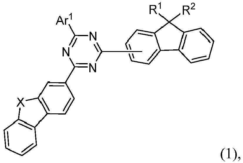
- X is O, S or Se;
- Ar1 is selected from C1 to C16 alkyl, substituted or unsubstituted C6 to C40 aryl, substituted or unsubstituted C3 to C40 heteroaryl, wherein
the substituents of the substituted C6 to C40 aryl and substituted C3 to C40 heteroaryl are selected from C1 to C16 alkyl, C1 to C16 alkoxy, partially or perfluorinated C1 to C16 alkyl, partially or perfluorinated C1 to C16 alkoxy, partially or perdeuterated C1 to C16 alkyl, C3 to C16 branched alkyl, C3 to C16 cyclic alkyl, C3 to C16 branched alkoxy, C3 to C16 cyclic alkoxy, partially or perdeuterated C1 to C16 alkoxy, C6 to C24 aryl, C3 to C25 heteroaryl, - PXR3R4, D, F or CN, wherein
R3, R4 are independently selected from C1 to C16 alkyl, C1 to C16 alkoxy, partially or perfluorinated C1 to C16 alkyl, partially or perfluorinated C1 to C16 alkoxy, partially or perdeuterated C1 to C16 alkyl, partially or perdeuterated C1 to C16 alkoxy, C6 to C18 aryl, C3 to C25 heteroaryl;
wherein the substituted C6 to C40 aryl and/or substituted C3 to C40 heteroaryl of Ar1 comprises at least one - PXR3R4 substituent; - R1, R2 are independently selected from substituted or unsubstituted C1 to C16 alkyl, substituted or unsubstituted C6 to C24 aryl, substituted or unsubstituted C3 to C24 heteroaryl, or R1 and R2 are selected from substituted or unsubstituted C6 to C24 aryl and substituted or unsubstituted C3 to C24 heteroaryl and linked with each other via a single bond such that a five-membered ring is formed,
wherein the substituents of the substituted C6 to C24 aryl and substituted C3 to C24 heteroarylene are selected from H, D, C1 to C16 alkyl, partially or perfluorinated C1 to C16 alkyl, partially or perdeuterated C1 to C16 alkyl, C1 to C16 alkoxy, C1 to C16 thioalkyl, C3 to C16 branched alkyl, C3 to C16 cyclic alkyl, C3 to C16 branched alkoxy, C3 to C16 cyclic alkoxy, C3 to C16 branched thioalkyl, C3 to C16 cyclic thioalkyl, C6 to C24 aryl and C3 to C25 heteroaryl;
- a dopant selected from an organic metal complex or metal halide.
- According to one embodiment, the organic semiconductor layer may comprise:
- a compound of formula 1:

- X is O, S or Se;
- Ar1 is selected from C1 to C16 alkyl, substituted or unsubstituted C6 to C40 aryl, substituted or unsubstituted C3 to C40 heteroaryl, wherein
the substituents of the substituted C6 to C40 aryl and substituted C3 to C40 heteroaryl are selected from - PXR3R4, wherein
R3, R4 are independently selected from C1 to C16 alkyl, C1 to C16 alkoxy, partially or perfluorinated C1 to C16 alkyl, partially or perfluorinated C1 to C16 alkoxy, partially or perdeuterated C1 to C16 alkyl, partially or perdeuterated C1 to C16 alkoxy, C6 to C18 aryl, C3 to C25 heteroaryl; - R1, R2 are independently selected from substituted or unsubstituted C1 to C16 alkyl, substituted or unsubstituted C6 to C24 aryl, substituted or unsubstituted C3 to C24 heteroaryl, or R1 and R2 are selected from substituted or unsubstituted C6 to C24 aryl and substituted or unsubstituted C3 to C24 heteroaryl and linked with each other via a single bond such that a five-membered ring is formed,
wherein the substituents of the substituted C6 to C24 aryl and substituted C3 to C24 heteroarylene are selected from H, D, C1 to C16 alkyl, partially or perfluorinated C1 to C16 alkyl, partially or perdeuterated C1 to C16 alkyl, C1 to C16 alkoxy, C1 to C16 thioalkyl, C3 to C16 branched alkyl, C3 to C16 cyclic alkyl, C3 to C16 branched alkoxy, C3 to C16 cyclic alkoxy, C3 to C16 branched thioalkyl, C3 to C16 cyclic thioalkyl, C6 to C24 aryl and C3 to C25 heteroaryl;
- a dopant selected from an organic metal complex or metal halide.
- According to one embodiment, the organic semiconductor layer may comprise:
- a compound of formula 1:

- X is O, S or Se;
- Ar1 is selected from C1 to C16 alkyl, substituted or unsubstituted C6 to C40 aryl, substituted or unsubstituted C3 to C40 heteroaryl, wherein
the substituents of the substituted C6 to C40 aryl and substituted C3 to C40 heteroaryl are selected from - PXR3R4, wherein - R3, R4 are independently selected from C1 to C16 alkyl, C1 to C16 alkoxy, partially or perfluorinated C1 to C16 alkyl, partially or perfluorinated C1 to C16 alkoxy, partially or perdeuterated C1 to C16 alkyl, partially or perdeuterated C1 to C16 alkoxy, C6 to C18 aryl, C3 to C25 heteroaryl;
- R1, R2 are independently selected from substituted or unsubstituted C1 to C16 alkyl, substituted or unsubstituted C6 to C24 aryl, substituted or unsubstituted C3 to C24 heteroaryl,
wherein the substituents of the substituted C6 to C24 aryl and substituted C3 to C24 heteroarylene are selected from H, D, C1 to C16 alkyl, partially or perfluorinated C1 to C16 alkyl, partially or perdeuterated C1 to C16 alkyl, C1 to C16 alkoxy, C1 to C16 thioalkyl, C3 to C16 branched alkyl, C3 to C16 cyclic alkyl, C3 to C16 branched alkoxy, C3 to C16 cyclic alkoxy, C3 to C16 branched thioalkyl, C3 to C16 cyclic thioalkyl, C6 to C24 aryl and C3 to C25 heteroaryl;
- a dopant selected from an organic metal complex or metal halide.
- According to one embodiment, the organic semiconductor layer may comprise:
- a compound of formula 1:

- X is O, S or Se;
- Ar1 is selected from C1 to C16 alkyl, unsubstituted C6 to C40 aryl, unsubstituted C3 to C40 heteroaryl;
- R1, R2 are independently selected from unsubstituted C1 to C16 alkyl, unsubstituted C6 to C24 aryl, unsubstituted C3 to C24 heteroaryl, or R1 and R2 are selected from unsubstituted C6 to C24 aryl and unsubstituted C3 to C24 heteroaryl and linked with each other via a single bond such that a five-membered ring is formed;
- a dopant selected from an organic metal complex or metal halide.
- According to one embodiment, the organic semiconductor layer may comprises:
- a compound of formula 1:

- X is O, S or Se;
- Ar1 is selected from C1 to C16 alkyl, unsubstituted C6 to C40 aryl, unsubstituted C3 to C40 heteroaryl;
- R1, R2 are independently selected from unsubstituted C1 to C16 alkyl, unsubstituted C6 to C24 aryl, unsubstituted C3 to C24 heteroaryl;
- a dopant selected from an organic metal complex or metal halide.
- According to one embodiment, the organic semiconductor layer may comprise:
- a compound of formula 1:

- X is O, S or Se;
- Ar1 is selected from substituted C6 to C40 aryl, substituted C3 to C40 heteroaryl, wherein the substituents of the substituted C6 to C40 aryl and substituted C3 to C40 heteroaryl is - PXR3R4, wherein
R3, R4 are independently selected from C1 to C16 alkyl, C1 to C16 alkoxy, partially or perfluorinated C1 to C16 alkyl, partially or perfluorinated C1 to C16 alkoxy, partially or perdeuterated C1 to C16 alkyl, partially or perdeuterated C1 to C16 alkoxy, C6 to C18 aryl, C3 to C25 heteroaryl; - R1, R2 are independently selected from substituted C1 to C16 alkyl, substituted C6 to C24 aryl, substituted C3 to C24 heteroaryl,
wherein the substituents of the substituted C6 to C24 aryl and substituted C3 to C24 heteroarylene are selected from H, D, C1 to C16 alkyl, partially or perfluorinated C1 to C16 alkyl, partially or perdeuterated C1 to C16 alkyl, C1 to C16 alkoxy, C1 to C16 thioalkyl, C3 to C16 branched alkyl, C3 to C16 cyclic alkyl, C3 to C16 branched alkoxy, C3 to C16 cyclic alkoxy, C3 to C16 branched thioalkyl, C3 to C16 cyclic thioalkyl, C6 to C24 aryl and C3 to C25 heteroaryl;
- a dopant selected from an organic metal complex or metal halide.
- According to another embodiment of the compound of formula 1, wherein X may be selected from O or S.
- According to another embodiment of the compound of formula 1, wherein X is O.
- According to another embodiment of the compound of formula 1, wherein
- R1, R2 are independently selected from substituted or unsubstituted C1 to C16 alkyl, substituted or unsubstituted C6 to C24 aryl, substituted or unsubstituted C3 to C24 heteroaryl,
wherein the substituents of the substituted C6 to C24 aryl and substituted C3 to C24 heteroarylene are selected from H, D, C1 to C16 alkyl, partially or perfluorinated C1 to C16 alkyl, partially or perdeuterated C1 to C16 alkyl, C1 to C16 alkoxy, C1 to C16 thioalkyl, C3 to C16 branched alkyl, C3 to C16 cyclic alkyl, C3 to C16 branched alkoxy, C3 to C16 cyclic alkoxy, C3 to C16 branched thioalkyl, C3 to C16 cyclic thioalkyl, C6 to C24 aryl and C3 to C25 heteroaryl. - According to another embodiment of the compound of formula 1, wherein
- R1, R2 are independently selected from substituted or unsubstituted C1 to C6 alkyl, substituted or unsubstituted C6 to C18 aryl, substituted or unsubstituted C3 to C17 heteroaryl,
wherein the substituents of the substituted C6 to C18 aryl and substituted C3 to C17 heteroarylene are selected from H, D, C1 to C6 alkyl, partially or perfluorinated C1 to C6 alkyl, partially or perdeuterated C1 to C6 alkyl, C1 to C6 alkoxy, C1 to C6 thioalkyl, C3 to C6 branched alkyl, C3 to C6 cyclic alkyl, C3 to C6 branched alkoxy, C3 to C6 cyclic alkoxy, C3 to C6 branched thioalkyl, C3 to C6 cyclic thioalkyl, C6 to C18 aryl and C3 to C17 heteroaryl. - According to another embodiment of the compound of formula 1, wherein
- R1, R2 are independently selected from unsubstituted C1 to C3 alkyl.
- According to another embodiment of the compound of formula 1, wherein
- R1, R2 are independently selected from substituted or unsubstituted C6 to C18 aryl, wherein the substituents of the substituted C6 to C18 aryl are selected from H, D, C1 to C6 alkyl, partially or perfluorinated C1 to C6 alkyl, partially or perdeuterated C1 to C6 alkyl, C1 to C6 alkoxy, preferably R1, R2 are independently selected from phenyl, biphenyl, terphenyl, naphthyl, phenanthrenyl, also preferred R1, R2 are selected from phenyl.
- According to another embodiment of the compound of formula 1, wherein
- R1, R2 are independently selected from substituted or unsubstituted C3 to C17 heteroaryl, wherein the substituents of the substituted C3 to C17 heteroaryl are selected from H, D, C1 to C6 alkyl, partially or perfluorinated C1 to C6 alkyl, partially or perdeuterated C1 to C6 alkyl, C1 to C6 alkoxy, preferably R1, R2 are independently selected from pyridyl, quinolinyl, quinazolinyl.
- According to another embodiment of the compound of formula 1, wherein R1, R2 are independently selected from unsubstituted unsubstituted C6 to C24 aryl, or unsubstituted C3 to C24 heteroaryl, preferably R1, R2 are independently selected from phenyl, biphenyl, terphenyl naphthyl, phenanthrenyl, pyridyl, quinolinyl, quinazolinyl, more preferred R1 is selected from phenyl, biphenyl, terphenyl naphthyl, phenanthrenyl and R2 is selected from pyridyl, quinolinyl, quinazolinyl.
- A high Tg may be achieved when R1, R2 are selected in this range.
- According to another embodiment of the compound of formula 1, wherein
- Ar1 may be selected from C1 to C12 alkyl, substituted or unsubstituted C6 to C24 aryl or substituted or unsubstituted C3 to C36 heteroaryl, wherein
the substituents of the substituted C6 to C24 aryl and substituted C3 to C36 heteroaryl may be selected from C1 to C12 alkyl, C1 to C12 alkoxy, C3 to C16 branched alkyl, C3 to C16 cyclic alkyl, C3 to C16 branched alkoxy, C3 to C16 cyclic alkoxy, partially or perfluorinated C1 to C12 alkyl, partially or perfluorinated C1 to C16 alkoxy, partially or perdeuterated C1 to C12 alkyl, partially or perdeuterated C1 to C16 alkoxy, C6 to C24 aryl, C3 to C25 heteroaryl, D, F or CN, preferably from C1 to C12 alkyl. - According to another embodiment of the compound of formula 1, wherein
- Ar1 may be selected from substituted or unsubstituted C6 to C18 aryl or substituted or unsubstituted C3 to C17 heteroaryl, wherein
the substituents of the substituted C6 to C18 aryl and substituted C3 to C17 heteroaryl may be selected from F or CN. - According to another embodiment of the compound of formula 1, wherein
- Ar1 may be selected from substituted or unsubstituted C6 to C18 aryl or substituted or unsubstituted C3 to C17 heteroaryl, wherein
the substituents of the substituted C6 to C18 aryl and substituted C3 to C17 heteroaryl may be selected from - PXR3R4, F or CN; - According to another embodiment of the compound of formula 1, wherein
- Ar1 may be selected from unsubstituted C6 to C24 aryl, preferably a C6 or C12 aryl.
- According to another embodiment of the compound of formula 1, wherein
- Ar1 may be selected from unsubstituted C6 to C12 aryl, or unsubstituted C3 to C18 heteroaryl, preferably phenyl or biphenyl and in addition preferred phenyl.
- In another embodiment, Ar1 may be selected from B1 to B6 and B16 to B23, preferably from B1 to B6, B16 to B17 and B19.
- According to another embodiment of the compound of formula 1, wherein
- Ar1 may be independently selected from B1 to B77, wherein
- a) B1 to B6 are substituted or unsubstituted non-heteroaryl groups:


- b) B7 to B23 are substituted or unsubstituted annelated non-heteroaryl groups:


- c) B24 to B31 are dibenzofurane/dibenzothiophene group:


- d) B32 to B34 are unsubstituted pyridine groups:

- e) B35 to B62 are unsubstituted or substituted hetero arylene groups:


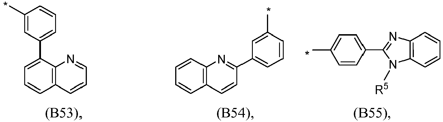


- f) B63 to B65 unsubstituted annelated hetero arylene groups:

- g) B66 and B67 are nitrile substituted phenyl groups

- h) B68 to B70 are nitrile substituted biphenyl groups

- i) B71 to B77 are carbazole groups

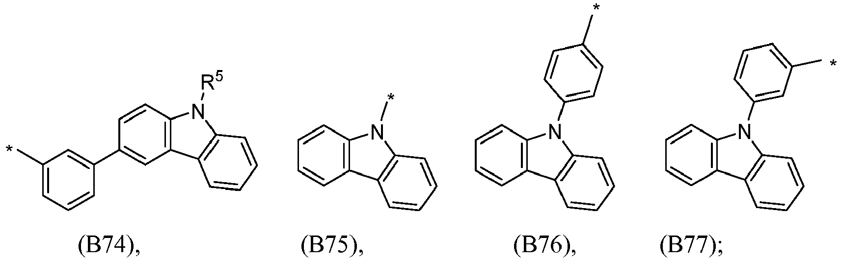
- a) B1 to B6 are substituted or unsubstituted non-heteroaryl groups:
- the substituent R5 may be independently selected from H, C1 to C16 alkyl, partially or perfluorinated C1 to C16 alkyl, partially or perdeuterated C1 to C16 alkyl, C1 to C16 alkoxy, C3 to C16 branched alkyl, C3 to C16 cyclic alkyl, C3 to C16 branched alkoxy, C3 to C16 cyclic alkoxy, C6 to C24 aryl and C3 to C25 heteroaryl.
- In another embodiment, Ar1 may be selected from B1 to B6 and B16 to B23, preferably from B1 to B6, B16 to B17 and B19.
- According to another embodiment of the compound of formula 1, the compound may be selected from D1 to D8:


- According to another embodiment of the compound of formula 1, wherein Ar1 may be independently selected from structures C1 to C5:


R3, R4 may be independently selected from C1 to C16 alkyl, C1 to C16 alkoxy, partially or perfluorinated C1 to C16 alkyl, partially or perfluorinated C1 to C16 alkoxy, partially or perdeuterated C1 to C16 alkyl, partially or perdeuterated C1 to C16 alkoxy, C6 to C18 aryl, C3 to C25 heteroaryl. - According to another embodiment of the compound of formula 1, wherein R3, R4 may be independently selected from C1 to C8 alkyl, C1 to C8 alkoxy, partially or perfluorinated C1 to C8 alkyl, partially or perfluorinated C1 to C8 alkoxy, partially or perdeuterated C1 to C8 alkyl, partially or perdeuterated C1 to C8 alkoxy, C6 to C12 aryl, C3 to C20 heteroaryl.
- According to another embodiment of the compound of formula 1, wherein R3, R4 may be independently selected from C1 to C8 alkyl, partially or perdeuterated C1 to C8 alkyl, partially or perdeuterated C1 to C8 alkoxy, C6 to C12 aryl, C3 to C20 heteroaryl.
- According to another embodiment of the compound of formula 1, wherein R3, R4 may be phenyl or C1 to C4 alkyl, even more preferred phenyl or methyl.
- According to another embodiment of the compound of formula 1, wherein R3 and R4 are selected the same.
- According to an aspect the organic semiconductor layer can be used as a layer for an organic electronic device. For example, the organic electronic device can be an OLED or there like.
- The organic semiconductor layer comprising a compound of formula 1 and a dopant selected from an organic metal complex or metal halide have strong electron transport characteristics to increase charge mobility and/or stability and thereby to improve luminance efficiency, voltage characteristics, and/or lifetime characteristics.
- The organic semiconductor layer comprising a compound of formula 1 and a dopant selected from an organic metal complex or metal halide have high electron mobility and a low operating voltage.
- The organic semiconductor layer comprising a compound of formula 1 and a dopant selected from an organic metal complex or metal halide may be non-emissive.
- In the context of the present specification the term "essentially non-emissive" or "non-emitting" means that the contribution of the compound of formula 1 or layer comprising the compound of formula 1 and the dopant to the visible emission spectrum from the device is less than 10 %, preferably less than 5 %, further preferred less than 1 %, relative to the visible emission spectrum. The visible emission spectrum is an emission spectrum with a wavelength of about ≥ 380 nm to about ≤ 780 nm. Preferably, the organic semiconductor layer comprising the compound of formula 1 is essentially non-emissive or non-emitting.
- The term "free of", "does not contain", "does not comprise" does not exclude impurities which may be present in the compounds prior to deposition. Impurities have no technical effect with respect to the object achieved by the present invention.
- The operating voltage, also named U, is measured in Volt (V) at 10 milliAmpere per square centimeter (mA/cm2).
- The candela per Ampere efficiency, also named cd/A efficiency, is measured in candela per ampere at 10 milliAmpere per square centimeter (mA/cm2).
- The external quantum efficiency, also named EQE, is measured in percent (%).
- The color space is described by coordinates CIE-x and CIE-y (International Commission on Illumination 1931). For blue emission the CIE-y is of particular importance. A smaller CIE-y denotes a deeper blue color.
- The highest occupied molecular orbital, also named HOMO, and lowest unoccupied molecular orbital, also named LUMO, are measured in electron volt (eV).
- The rate onset temperature is measured in °C and describes the VTE source temperature at which measurable evaporation of a compound commences at a pressure of less than 10-5 mbar.
- The term "OLED", "organic light emitting diode", "organic light emitting device", "organic optoelectronic device" and "organic light-emitting diode" are simultaneously used and have the same meaning.
- The term "transition metal" means and comprises any element in the d-block of the periodic table, which comprises groups 3 to 12 elements on the periodic table.
- The term "group III to VI metal" means and comprises any metal in groups III to VI of the periodic table.
- As used herein, "weight percent", "wt.-%", "percent by weight", "% by weight", and variations thereof refer to a composition, component, substance or agent as the weight of that composition, component, substance or agent of the respective electron transport layer divided by the total weight of the composition thereof and multiplied by 100. It is understood that the total weight percent amount of all components, substances or agents of the respective electron transport layer are selected such that it does not exceed 100 wt.-%.
- As used herein, "volume percent", "vol.-%", "percent by volume", "% by volume", and variations thereof refer to an elemental metal, a composition, component, substance or agent as the volume of that elemental metal, component, substance or agent of the respective electron transport layer divided by the total volume of the respective electron transport layer thereof and multiplied by 100. It is understood that the total volume percent amount of all elemental metal, components, substances or agents of the respective cathode electrode layer are selected such that it does not exceed 100 vol.-%.
- All numeric values are herein assumed to be modified by the term "about", whether or not explicitly indicated. As used herein, the term "about" refers to variation in the numerical quantity that can occur.
- Whether or not modified by the term "about", the claims include equivalents to the quantities.
- It should be noted that, as used in this specification and the appended claims, the singular forms "a", "an", and "the" include plural referents unless the content clearly dictates otherwise.
- It should be noted that, as used in this specification and the appended claims, "*" if not otherwise defined indicates the chemical bonding position.
- The anode electrode and cathode electrode may be described as anode electrode / cathode electrode or anode electrode / cathode electrode or anode electrode layer / cathode electrode layer.
- According to another aspect, an organic optoelectronic device comprises an anode layer and a cathode layer facing each other and at least one organic semiconductor layer between the anode layer and the cathode layer, wherein the organic semiconductor layer comprises or consists of the compound of formula 1.
- According to yet another aspect, a display device comprising the organic electronic device, which can be an organic optoelectronic device, is provided.
- In the present specification, when a definition is not otherwise provided, an "alkyl group" may refer to an aliphatic hydrocarbon group. The alkyl group may refer to "a saturated alkyl group" without any double bond or triple bond. The alkyl group may be a linear, cyclic or branched alkyl group.
- The alkyl group may be a C1 to C16 alkyl group, or preferably a C1 to C12 alkyl group. More specifically, the alkyl group may be a C1 to C14 alkyl group, or preferably a C1 to C10 alkyl group or a C1 to C6 alkyl group. For example, a C1 to C4 alkyl group comprises 1 to 4 carbons in alkyl chain, and may be selected from methyl, ethyl, propyl, iso-propyl, n-butyl, iso-butyl, sec-butyl, and t-butyl.
- Specific examples of the alkyl group may be a methyl group, an ethyl group, a propyl group, an isopropyl group, a butyl group, an isobutyl group, a tert-butyl group, a pentyl group, a hexyl group, a cyclopropyl group, a cyclobutyl group, a cyclopentyl group, a cyclohexyl group, and the like.
- In the present specification "arylene group" may refer to a group comprising at least one hydrocarbon aromatic moiety, and all the elements of the hydrocarbon aromatic moiety may have p-orbitals which form conjugation, for example a phenyl group, a naphthyl group, an anthracenyl group, a phenanthrenyl group, a pyrenyl group, a fluorenyl group and the like.
- The term "heteroarylene" may refer to aromatic heterocycles with at least one heteroatom, and all the elements of the hydrocarbon heteroaromatic moiety may have p-orbitals which form conjugation.
- The term "hetero-fluorene ring" refers to a dibenzo[d,d]furanyl, dibenzo[b,d]thiophenyl or dibenzo[b,d]selenophenyl group.
- The heteroatom may be selected from N, O, S, B, Si, P, Se, preferably from N, O and S.
- A heteroarylene ring may comprise at least 1 to 3 heteroatoms. Preferably a heteroarylene ring may comprise at least 1 to 3 heteroatoms individually selected from N, S and/or O.
- Further preferred in addition to the group of formula 1 at least one additional heteroaryl/ene ring may comprise at least 1 to 3 N-atoms, or at least 1 to 2-N atoms or at least one N-atom.
- According to another preferred embodiment the compound according to formula 1 may comprise:
- at least 6 to 25 aromatic rings, preferably at least 7 to 22 aromatic rings, further preferred at least 8 to 20 aromatic rings, in addition preferred at least 9 to 15 aromatic rings and more preferred at least 10 to 14 aromatic rings; wherein
- at least 2 to 5, preferably 3 to 4 or 2 to 3 are heteroaromatic rings.
- According to one embodiment the compound according to formula 1:
- comprises at least about 6 to about 20 aromatic rings, preferably at least about 7 to about 18 aromatic rings, further preferred at least about 9 to about 16 aromatic rings, in addition preferred at least about 10 to about 15 aromatic rings and more preferred at least about 11 to about 14 aromatic rings; and/or
- the compound of formula 1 comprises at least about 2 to about 6, preferably about 3 to about 5 or about 2 to about 4, hetero aromatic rings, wherein the hetero atoms can be selected from N, O, S; and/or
- comprises at least one fluorene ring and at least one hetero-fluorene ring, wherein the hetero atoms can be selected from N, O, S; and/or
- comprises at least one ring, or at least two rings.
- According to a further preferred embodiment the compound of formula 1 comprises at least 2 to 7, preferably 2 to 5, or 2 to 3 hetero aromatic rings.
- According to a further preferred embodiment the compound of formula 1 comprises at least 2 to 7, preferably 2 to 5, or 2 to 3 hetero aromatic rings, wherein at least one of the aromatic rings is a five member hetero aromatic ring.
- According to a further preferred embodiment the compound of formula 1 comprises at least 3 to 7, preferably 3 to 6, or 3 to 5 hetero aromatic rings, wherein at least two of the hetero aromatic rings are five member hetero-aromatic-rings.
- According to one embodiment the compound according to formula 1 may comprise at least 6 to 12 non-hetero aromatic rings and 2 to 3 hetero aromatic rings.
- According to one preferred embodiment the compound according to formula 1 may comprise at least 7 to 12 non-hetero aromatic rings and 2 to 5 hetero aromatic rings.
- According to one preferred embodiment the compound according to formula 1 may comprise at least 7 to 11 non-hetero aromatic rings and 2 to 3 hetero aromatic rings.
- The melting point (mp) is determined as peak temperatures from the DSC curves of the above TGA-DSC measurement or from separate DSC measurements (Mettler Toledo DSC822e, heating of samples from room temperature to completeness of melting with heating rate 10 K/min under a stream of pure nitrogen. Sample amounts of 4 to 6 mg are placed in a 40 µL Mettler Toledo aluminum pan with lid, a <1 mm hole is pierced into the lid).
- According to another embodiment the compound of formula 1 may have a melting point of about ≥ 250° C and about ≤ 380° C, preferably about ≥ 260° C and about ≤ 370° C, further preferred about ≥ 270° C and about ≤ 360° C, in addition preferred about ≥ 275° C and about ≤ 350° C, also preferred about ≥ 280° C and about ≤ 340° C, likewise preferred about ≥ 285° C and about ≤ 330° C and more preferred about ≥ 290° C and about ≤ 310° C.
- The glass transition temperature is measured under nitrogen and using a heating rate of 10 K per min in a Mettler Toledo DSC 822e differential scanning calorimeter as described in DIN EN ISO 11357, published in March 2010.
- According to another embodiment the compound of formula 1 may have a glass transition temperature Tg of about ≥ 120° C and about ≤ 380° C, preferably about ≥ 130° C and about ≤ 350° C, further preferred about ≥ 140° C and about ≤ 320° C, in addition preferred about ≥ 140° C and about ≤ 200° C and also preferred about ≥ 140° C and about ≤ 180° C.
- The rate onset temperature is determined by loading 100 mg compound into a VTE source. The VTE source is heated at a constant rate of 15 K/min at a pressure of less than 10-5 mbar and the temperature inside the source measured with a thermocouple. Evaporation of the compound is detected with a QCM detector which detects deposition of the compound on the quartz crystal of the detector. The deposition rate on the quartz crystal is measured in Ǻngstrom per second. To determine the rate onset temperature, the deposition rate is plotted against the VTE source temperature. The rate onset is the temperature at which noticeable deposition on the QCM detector occurs. For accurate results, the VTE source is heated and cooled three time and only results from the second and third run are used to determine the rate onset temperature.
- To achieve good control over the evaporation rate of an organic compound, the rate onset temperature may be in the range of 200 to 255 °C. If the rate onset temperature is below 200 °C the evaporation may be too rapid and therefore difficult to control. If the rate onset temperature is above 255 °C the evaporation rate may be too low which may result in low takt time and decomposition of the organic compound in VTE source may occur due to prolonged exposure to elevated temperatures.
- The rate onset temperature is an indirect measure of the volatility of a compound. The higher the rate onset temperature the lower is the volatility of a compound.
- According to another embodiment the compound of formula 1 may have a rate onset temperature TRO of about ≥ 200° C and about ≤ 350° C, preferably about ≥ 220° C and about ≤ 350° C, further preferred about ≥ 240° C and about ≤ 320° C, in addition preferred about ≥ 240° C and about ≤ 300° C and more preferred about ≥ 240° C and about ≤ 280° C.
- The dipole moment |
µ |of a molecule containing N atoms is given by:

r i are the partial charge and position of atom i in the molecule. - The dipole moment is determined by a semi-empirical molecular orbital method. The geometries of the molecular structures are optimized using the hybrid functional B3LYP with the 6-31G* basis set in the gas phase as implemented in the program package TURBOMOLE V6.5. If more than one conformation is viable, the conformation with the lowest total energy is selected to determine the bond lengths of the molecules.
- According to one embodiment the compounds according to formula 1 may have a dipole moment (Debye) in the range from about ≥ 0.25 to about ≤ 1.50, preferably from about ≥ 0.28 to about ≤ 1.00, further preferred from about ≥ 0.30 to about ≤ 0.70, also preferred from about ≥ 0.32 to about ≤ 0.60.
- The HOMO and LUMO are calculated with the program package TURBOMOLE V6.5. The optimized geometries and the HOMO and LUMO energy levels of the molecular structures are determined by applying the hybrid functional B3LYP with a 6-31G* basis set in the gas phase. If more than one conformation is viable, the conformation with the lowest total energy is selected.
- According to one embodiment the compounds according to formula 1 may have a LUMO energy level (eV) in the range from about - 2.10 eV to about - 1.90 eV, preferably from about - 1.99 eV to about - 1.91 eV, further preferred from about - 1.98 eV to about - 1.92 eV, also preferred from about - 1.97 eV to about - 1.93 eV.
- To determine the distribution of the LUMO in the materials, the isosurfaces of the orbitals are plotted in the graphical user interface TMolex Version 3.3. The 3D data for this property is generated using a coarse grid and a value of 0.03 was chosen to plot the positive and negative iso-densities of the isosurfaces.
- Surprisingly, it was found that the compounds of formula 1 and the inventive organic electronic devices solve the problem underlying the present invention by being superior over the organic electroluminescent devices and compounds known in the art, in particular with respect to cd/A efficiency, also referred to as current efficiency and to lifetime. At the same time the operating voltage is kept at a similar or even improved level which is important for reducing power consumption and increasing battery life, for example of a mobile display device. High cd/A efficiency is important for high efficiency and thereby increased battery life of a mobile device, for example a mobile display device. Long lifetime at high current density is important for the longevity of a device which is run at high brightness.
- Additionally, it was surprisingly found that the calculated LUMO level of compounds of formula 1 is significantly more negative than the LUMO of the state of the art. A more negative LUMO may be beneficial for improved electron transfer from the cathode to the emission layer.
- Additionally, it was found that in compounds of formula 1 the LUMO is delocalized over the atoms in the triazine group and over the majority of atoms in the dibenzo[d,d]furanyl, dibenzo[b,d]thiophenyl or dibenzo[b,d]selenophenyl group and in the triazinyl group. Without being bound by theory, more efficient electron transfer from neighbouring molecules and/or the cathode and/or improved stability of the molecule itself may be achieved when the LUMO is delocalized over the atoms in the triazine group and over the majority of atoms in the dibenzo[d,d]furanyl, dibenzo[b,d]thiophenyl or dibenzo[b,d]selenophenyl group and in the triazinyl group.
- Futhermore, it was found that compounds of formula 1 have a high Tg. A high Tg may be beneficial for improved stability of the organic semiconductor layer, in particular at elevated temperatures, for example for application in automobiles.
- The inventors have surprisingly found that particular good performance can be achieved when using the organic electroluminescent device as a fluorescent blue device.
- The specific arrangements mentioned herein as preferred were found to be particularly advantageous.
- Likewise, some compounds falling within the scope of the broadest definition of the present invention have surprisingly be found to be particularly well performing with respect to the mentioned property of cd/A efficiency and/or lifetime. These compounds are discussed herein to be particularly preferred.
- Further an organic optoelectronic device having high efficiency and/or long lifetime may be realized.
- A material for the anode may be a metal or a metal oxide, or an organic material, preferably a material with work function above about 4.8 eV, more preferably above about 5.1 eV, most preferably above about 5.3 eV. Preferred metals are noble metals like Pt, Au or Ag, preferred metal oxides are transparent metal oxides like ITO or IZO which may be advantageously used in bottom-emitting OLEDs having a reflective cathode.
- In devices comprising a transparent metal oxide anode or a reflective metal anode, the anode may have a thickness from about 50 nm to about 100 nm, whereas semitransparent metal anodes may be as thin as from about 5 nm to about 15 nm, and non-transparent metal anodes may have a thickness from about 15 nm to about 150nm.
- The hole injection layer may improve interface properties between the anode and an organic material used for the hole transport layer, and is applied on a non-planarized anode and thus may planarize the surface of the anode. For example, the hole injection layer may include a material having a median value of the energy level of its highest occupied molecular orbital (HOMO) between the work function of the anode material and the energy level of the HOMO of the hole transport layer, in order to adjust a difference between the work function of the anode and the energy level of the HOMO of the hole transport layer.
- When the hole transport region comprises a hole injection layer 36, the hole injection layer may be formed on the anode by any of a variety of methods, for example, vacuum deposition, spin coating, casting, Langmuir-Blodgett (LB) method, or the like.
- When hole injection layer is formed using vacuum deposition, vacuum deposition conditions may vary depending on the material that is used to form the hole injection layer, and the desired structure and thermal properties of the hole injection layer to be formed and for example, vacuum deposition may be performed at a temperature of about 100 °C to about 500 °C, a pressure of about 10-6 Pa to about 10-1 Pa, and a deposition rate of about 0.1 to about 10 nm/sec, but the deposition conditions are not limited thereto.
- When the hole injection layer is formed using spin coating, the coating conditions may vary depending on the material that is used to form the hole injection layer, and the desired structure and thermal properties of the hole injection layer to be formed. For example, the coating rate may be in the range of about 2000 rpm to about 5000 rpm, and a temperature at which heat treatment is performed to remove a solvent after coating may be in a range of about 80 °C to about 200 °C, but the coating conditions are not limited thereto.
- The hole injection layer may further comprise a p-dopant to improve conductivity and/or hole injection from the anode.
- In another aspect, the p-dopant may be homogeneously dispersed in the hole injection layer.
- In another aspect, the p-dopant may be present in the hole injection layer in a higher concentration closer to the anode and in a lower concentration closer to the cathode.
- The p-dopant may be one of a quinone derivative or a radialene compound but not limited thereto. Non-limiting examples of the p-dopant are quinone derivatives such as tetracyanoquinonedimethane (TCNQ), 2,3,5,6-tetrafluoro-tetracyano-1,4-benzoquinonedimethane (F4-TCNQ), 4,4',4"-((1E,1'E,1"E)-cyclopropane-1,2,3-triylidenetris(cyanomethanylylidene))-tris(2,3,5,6-tetrafluorobenzonitrile).
- Acccording to another embodiment, an organic electronic device comrising an organic semiconductor layer that comprises a compound of formula 1 and a dopant selected from an organic metal complex or metal halide may additional comprise a layer comprising a radialene compound and/or a quinodimethane compound.
- In another embodiment, the radialene compound and/or the quinodimethane compound may be substituted with one or more halogen atoms and/or with one or more electron withdrawing groups. Electron withdrawing groups can be selected from nitrile groups, halogenated alkyl groups, alternatively from perhalogenated alkyl groups, alternatively from perfluorinated alkyl groups. Other examples of electron withdrawing groups may be acyl, sulfonyl groups or phosphoryl groups.
- Alternatively, acyl groups, sulfonyl groups and/or phosphoryl groups may comprise halogenated and/or perhalogenated hydrocarbyl. In one embodiment, the perhalogenated hydrocarbyl may be a perfluorinated hydrocarbyl. Examples of a perfluorinated hydrocarbyl can be perfluormethyl, perfluorethyl, perfluorpropyl, perfluorisopropyl, perfluorobutyl, perfluorophenyl, perfluorotolyl; examples of sulfonyl groups comprising a halogenated hydrocarbyl may be trifluoromethylsulfonyl, pentafluoroethylsulfonyl, pentafluorophenylsulfonyl, heptafluoropropylsufonyl, nonafluorobutylsulfonyl, and like.
- In one embodiment, the radialene and/or the quinodimethane compound may be comprised in a hole injection, hole transporting and/or a hole generation layer.
- In one embodiment, the radialene compound may have formula (XX) and/or the quinodimethane compound may have formula (XXIa) or (XXIb):


- Conditions for forming the hole transport layer and the electron blocking layer may be defined based on the above-described formation conditions for the hole injection layer.
- A thickness of the hole transport part of the charge transport region may be from about 10 nm to about 1000 nm, for example, about 10 nm to about 100 nm. When the hole transport part of the charge transport region comprises the hole injection layer and the hole transport layer, a thickness of the hole injection layer may be from about 10 nm to about 1000 nm, for example about 10 nm to about 100 nm and a thickness of the hole transport layer may be from about 5 nm to about 200 nm, for example about 10 nm to about 150 nm. When the thicknesses of the hole transport part of the charge transport region, the HIL, and the HTL are within these ranges, satisfactory hole transport characteristics may be obtained without a substantial increase in operating voltage.
- Hole transport matrix materials used in the hole transport region are not particularly limited. Preferred are covalent compounds comprising a conjugated system of at least 6 delocalized electrons, preferably organic compounds comprising at least one aromatic ring, more preferably organic compounds comprising at least two aromatic rings, even more preferably organic compounds comprising at least three aromatic rings, most preferably organic compounds comprising at least four aromatic rings. Typical examples of hole transport matrix materials which are widely used in hole transport layers are polycyclic aromatic hydrocarbons, triarylene amine compounds and heterocyclic aromatic compounds. Suitable ranges of frontier orbital energy levels of hole transport matrices useful in various layer of the hole transport region are well-known. In terms of the redox potential of the redox couple HTL matrix/ cation radical of the HTL matrix, the preferred values (if measured for example by cyclic voltammetry against ferrocene/ferrocenium redox couple as reference) may be in the range 0.0 - 1.0 V, more preferably in the range 0.2 - 0.7 V, even more preferably in the range 0.3 - 0.5 V.
- The hole transport part of the charge transport region may further include a buffer layer.
- Buffer layer that can be suitable used are disclosed in
US 6 140 763 ,US 6 614 176 and inUS2016/248022 . - The buffer layer may compensate for an optical resonance distance of light according to a wavelength of the light emitted from the EML, and thus may increase efficiency.
- The emission layer may be formed on the hole transport region by using vacuum deposition, spin coating, casting, LB method, or the like. When the emission layer is formed using vacuum deposition or spin coating, the conditions for deposition and coating may be similar to those for the formation of the hole injection layer, though the conditions for the deposition and coating may vary depending on the material that is used to form the emission layer. The emission layer may include an emitter host (EML host) and an emitter dopant (further only emitter).
- A thickness of the emission layer may be about 100Å to about 1000Å, for example about 200Å to about 600Å. When the thickness of the emission layer is within these ranges, the emission layer may have improved emission characteristics without a substantial increase in operating voltage.
- According to another embodiment, the emission layer comprises compound of formula 1 as emitter host.
- The emitter host compound has at least three aromatic rings, which are independently selected from carbocyclic rings and heterocyclic rings.
- Other compounds that can be used as the emitter host is an anthracene matrix compound represented by formula 400 below:

- In formula 400, Arm and Ar112 may be each independently a substituted or unsubstituted C6-C60 arylene group; Ar113 to Ar116 may be each independently a substituted or unsubstituted C1-C10 alkyl group or a substituted or unsubstituted C6-C60 arylene group; and g, h, i, and j may be each independently an integer from 0 to 4.
- In some embodiments, Ar111 and Ar112 in formula 400 may be each independently one of a phenylene group, a naphthalene group, a phenanthrenylene group, or a pyrenylene group; or
a phenylene group, a naphthalene group, a phenanthrenylene group, a fluorenyl group, or a pyrenylene group, each substituted with at least one of a phenyl group, a naphthyl group, or an anthryl group. - In formula 400, g, h, i, and j may be each independently an integer of 0, 1, or 2.
- In formula 400, Ar113 to Ar116 may be each independently one of
- a C1-C10 alkyl group substituted with at least one of a phenyl group, a naphthyl group, or an anthryl group;
- a phenyl group, a naphthyl group, an anthryl group, a pyrenyl group, a phenanthrenyl group, or a fluorenyl group;
- a phenyl group, a naphthyl group, an anthryl group, a pyrenyl group, a phenanthrenyl group, or a fluorenyl group, each substituted with at least one of a deuterium atom, a halogen atom, a hydroxyl group, a cyano group, a nitro group, an amino group, an amidino group, a hydrazine group, a hydrazone group, a carboxyl group or a salt thereof,
- a sulfonic acid group or a salt thereof, a phosphoric acid group or a salt thereof, - a C1-C60 alkyl group, a C2-C60 alkenyl group, a C2-C60 alkynyl group, a C1-C60 alkoxy group, a phenyl group, a naphthyl group, an anthryl group, a pyrenyl group, a phenanthrenyl group, or
- a fluorenyl group

- formulas 7 or 8

- Wherein in the formulas 7 and 8, X is selected form an oxygen atom and a sulfur atom, but embodiments of the invention are not limited thereto.
- In the formula 7, any one of R11 to R14 is used for bonding to Arm. R11 to R14 that are not used for bonding to Arm and R15 to R20 are the same as R1 to R8.
- In the formula 8, any one of R21 to R24 is used for bonding to Arm. R21 to R24 that are not used for bonding to Ar111 and R25 to R30 are the same as R1 to R8.
- Preferably, the EML host comprises between one and three heteroatoms selected from the group consisting of N, O or S. More preferred the EML host comprises one heteroatom selected from S or O.
- The dopant is mixed in a small amount to cause light emission, and may be generally a material such as a metal complex that emits light by multiple excitation into a triplet or more. The dopant may be, for example an inorganic, organic, or organic/inorganic compound, and one or more kinds thereof may be used.
- The emitter may be a red, green, or blue emitter.
- The dopant may be a fluorescent dopant, for example ter-fluorene, the structures are shown below. 4.4'-bis(4-diphenyl amiostyryl)biphenyl (DPAVBI, 2,5,8,11-tetra-tert-butyl perylene (TBPe), and Compound 8 below are examples of fluorescent blue dopants.

- The dopant may be a phosphorescent dopant, and examples of the phosphorescent dopant may be an organic metal compound comprising Ir, Pt, Os, Ti, Zr, Hf, Eu, Tb, Tm, Fe, Co, Ni, Ru, Rh, Pd, or a combination thereof. The phosphorescent dopant may be, for example a compound represented by formula Z, but is not limited thereto:
J2MX (Z).
- In formula Z, M is a metal, and J and X are the same or different, and are a ligand to form a complex compound with M.
- The M may be, for example Ir, Pt, Os, Ti, Zr, Hf, Eu, Tb, Tm, Fe, Co, Ni, Ru, Rh, Pd or a combination thereof, and the J and X may be, for example a bidendate ligand.
- One or more emission layers may be arranged between the anode and the cathode. To increase overall performance, two or more emission layers may be present.
- A charge generation layer (also named CGL) may be arranged between the first and the second emission layer, and second and third emission layer, if present. Typically, the CGL comprises a n-type charge generation layer (also named n-CGL or electron generation layer) and a p-type charge generation layer (also named p-CGL or hole generation layer). An interlayer may be arranged between the n-type CGL and the p-type CGL.
- In one aspect, the n-type CGL may comprise a compound of formula 1. The n-type CGL , further comprises a metal, metal salt or organic metal complex, preferably a metal. The metal may be selected from an alkali, alkaline earth or rare earth metal.
- The p-type CGL may comprise a dipyrazino[2,3-f:2',3'-h]quinoxaline, a quinone compound or a radialene compound, preferably dipyrazino[2,3-f:2',3'-h]quinoxaline-2,3,6,7,10,11-hexacarbonitrile or a compound or formula (XX) and/or a compound of formula (XXIa) or (XXIb).
- According to another embodiment, the organic semiconductor layer that comprises compound of formula 1 is an electron transport layer. In another embodiment the electron transport layer may consist of compound of formula 1.
- For example, an organic light emitting diode according to an embodiment of the present invention comprises at least one electron transport layer, and in this case, the electron transport layer comprises compound of formula 1, or preferably of at least one compound of formulae D1 to D8.
- In another embodiment, the organic electronic device comprises an electron transport region of a stack of organic layers formed by two or more electron transport layers, wherein at least one electron transport layer comprises compound of formula 1 and a dopant selected from an organic metal complex or metal halide.
The electron transport layer may include one or two or more different electron transport compounds. - According to another embodiment, a first and a second electron transport layers comprise compound of formula 1 and a dopant selected from an organic metal complex or metal halide, wherein the compound of formula 1 is not selected the same.
- The thickness of the first electron transport layer may be from about 0.5 nm to about 100 nm, for example about 2 nm to about 40 nm. When the thickness of the first electron transport layer is within these ranges, the first electron transport layer may have improved electron transport ability without a substantial increase in operating voltage.
- A thickness of an optional second electron transport layer may be about 1 nm to about 100 nm, for example about 2 nm to about 20 nm. When the thickness of the electron transport layer is within these ranges, the electron transport layer may have satisfactory electron transporting ability without a substantial increase in operating voltage.
- The dopant of the electron transport layer may be a monovalent or divalent metal halide or an organic monovalent or divalent metal complex, preferably an alkali halide and/or alkali organic complex.
- According to another embodiment, the first and second electron transport layers comprise compound of formula 1, wherein the second electron transport layer further comprises the dopant selected from an organic metal complex or metal halide, preferably an alkali halide and/or alkali organic complex.
- Alkali halides that can be suitable used as the dopant (metal halide), also known as alkali metal halides, are the family of inorganic compounds with the chemical formula MX, where M is an alkali metal and X is a halogen.
- M can be selected from Li, Na, Potassium, Rubidium and Cesium.
- X can be selected from F, Cl, Br and J.
- According to various embodiments of the present invention a lithium halide may be preferred. The lithium halide can be selected from the group comprising LiF, LiCl, LiBr and LiJ. However, most preferred is LiF.
- The alkali halide is essentially non-emissive or non-emissive.
- The alkali organic complex that can be suitable used as the dopant as organic metal complex comprises an alkali metal and at least one organic ligand. The alkali metal is preferably selected from lithium.
- According to various embodiments of the present invention the organic ligand of the lithium organic complex is a quinolate, a borate, a phenolate, a pyridinolate or a Schiff base ligand;
- preferably the lithium quinolate complex has the formula III, IV or V:

- A1 to A6 are same or independently selected from CH, CR, N and O;
- R is same or independently selected from hydrogen, halogen, alkyl or arylene or heteroarylene with 1 to 20 carbon atoms; and more preferred A1 to A6 are CH;
- preferably the borate based organic ligand is a tetra(1H-pyrazol-1-yl)borate;
- preferably the phenolate is a 2-(pyridin-2-yl)phenolate, a 2-(diphenylphosphoryl)phenolate, an imidazol phenolates, or 2-(pyridin-2-yl)phenolate and more preferred 2-(1-phenyl-1H-benzo[d]imidazol-2-yl)phenolate;
- preferably the pyridinolate is a 2-(diphenylphosphoryl)pyridin-3-olate.
- According to various embodiments of the present invention the organic ligand of the alkali organic complex, preferably of a lithium organic complex, can be a quinolate. Quinolates that can be suitable used are disclosed in
WO 2013079217 A1 and incorporated by reference. - According to various embodiments of the present invention the organic ligand of the lithium organic complex can be a borate based organic ligand, Preferably the lithium organic complex is a lithium tetra(1H-pyrazol-1-yl)borate. Borate based organic ligands that can be suitable used are disclosed in
WO 2013079676 A1 and incorporated by reference. - According to various embodiments of the present invention the organic ligand of the lithium organic complex can be a phenolate ligand, Preferably the lithium organic complex is a lithium 2-(diphenylphosphoryl)phenolate. Phenolate ligands that can be suitable used are disclosed in
WO 2013079678 A1 and incorporated by reference. - Further, phenolate ligands can be selected from the group of pyridinolate, preferably 2-(diphenylphosphoryl)pyridin-3-olate. Pyridine phenolate ligands that can be suitable used are disclosed in
JP 2008195623 - In addition, phenolate ligands can be selected from the group of imidazol phenolates, preferably 2-(1-phenyl-1H-benzo[d]imidazol-2-yl)phenolate. Imidazol phenolate ligands that can be suitable used are disclosed in
JP 2001291593 - Also, phenolate ligands can be selected from the group of oxazol phenolates, preferably 2-(benzo[d]oxazol-2-yl)phenolate. Oxazol phenolate ligands that can be suitable used are disclosed in
US 20030165711 and incorporated by reference. - The alkali organic complex may be essentially non-emissive.
- According to another aspect of the invention, the organic electroluminescent device may further comprise an electron injection layer between the electron transport layer (first-ETL) and the cathode.
- The electron injection layer (EIL) may facilitate injection of electrons from the cathode.
- According to another aspect of the invention, the electron injection layer comprises:
- (i) an electropositive metal selected from alkali metals, alkaline earth metals and rare earth metals in substantially elemental form, preferably selected from Li, Na, K, Rb, Cs, Mg, Ca, Sr, Ba, Eu and Yb, more preferably from Li, Na, Mg, Ca, Sr and Yb, even more preferably from Li and Yb, most preferably Yb; and/or
- (ii) an alkali metal complex and/or alkali metal salt, preferably the Li complex and/or salt, more preferably a Li quinolinolate, even more preferably a lithium 8-hydroxyquinolinolate, most preferably the alkali metal salt and/or complex of the second electron transport layer (second-ETL) is identical with the alkali metal salt and/or complex of the injection layer.
- The electron injection layer may include at least one selected from LiF, NaCl, CsF, Li2O, and BaO.
- A thickness of the EIL may be from about 0.1 nm to about 10 nm, or about 0.3 nm to about 9 nm. When the thickness of the electron injection layer is within these ranges, the electron injection layer may have satisfactory electron injection ability without a substantial increase in operating voltage.
- The electron injection layer may comprise a compound of formula 1.
- A material for the cathode may be a metal, an alloy, or an electrically conductive compound that have a low work function, or a combination thereof. Specific examples of the material for the cathode may be lithium (Li), magnesium (Mg), aluminum (Al), aluminum-lithium (Al-Li), calcium (Ca), magnesium-indium (Mg-In), magnesium-silver (Mg-Ag), silver (Ag) etc. In order to manufacture a top-emission light-emitting device having a reflective anode deposited on a substrate, the cathode may be formed as a light-transmissive electrode from, for example, indium tin oxide (ITO), indium zinc oxide (IZO) or silver (Ag).
- In devices comprising a transparent metal oxide cathode or a reflective metal cathode, the cathode may have a thickness from about 50 nm to about 100 nm, whereas semitransparent metal cathodes may be as thin as from about 5 nm to about 15 nm.
- A substrate may be further disposed under the anode or on the cathode. The substrate may be a substrate that is used in a general organic light emitting diode and may be a glass substrate or a transparent plastic substrate with strong mechanical strength, thermal stability, transparency, surface smoothness, ease of handling, and water resistance.
- Hereinafter, the embodiments are illustrated in more detail with reference to examples. However, the present disclosure is not limited to the following examples.
- These and/or other aspects and advantages of the present invention will become apparent and more readily appreciated from the following description of the exemplary embodiments, taken in conjunction with the accompanying drawings, of which:
- FIG. 1
- is a schematic sectional view of an organic light-emitting diode (OLED), according to an exemplary embodiment of the present invention with an emission layer, one electron transport layer and an electron injection layer;
- FIG. 2
- is a schematic sectional view of an organic light-emitting diode (OLED), according to an exemplary embodiment of the present invention with an emission layer and two electron transport layers;
- FIG. 3
- is a schematic sectional view of an OLED, according to an exemplary embodiment of the present invention with an emission layer and three electron transport layers;
- FIG. 4
- is a schematic sectional view of an organic light-emitting diode (OLED), according to an exemplary embodiment of the present invention with an emission layer and one electron transport layer;
- FIG. 5
- is a schematic sectional view of an organic light-emitting diode (OLED), according to an exemplary embodiment of the present invention with an emission layer and two electron transport layers;
- FIG. 6
- is a schematic sectional view of an OLED, according to an exemplary embodiment of the present invention with an emission layer and three electron transport layers.
- Reference will now be made in detail to the exemplary aspects, examples of which are illustrated in the accompanying drawings, wherein like reference numerals refer to the like elements throughout. The exemplary embodiments are described below, in order to explain the aspects, by referring to the figures.
- Herein, when a first element is referred to as being formed or disposed "on" a second element, the first element can be disposed directly on the second element, or one or more other elements may be disposed there between. When a first element is referred to as being formed or disposed "directly on" a second element, no other elements are disposed there between.
- The term "contacting sandwiched" refers to an arrangement of three layers whereby the layer in the middle is in direct contact with the two adjacent layers.
- The organic light emitting diodes according to an embodiment of the present invention may include a hole transport region; an emission layer; and a first electron transport layer comprising a compound according to formula 1 and a dopant selected from an organic metal complex or metal halide.
-
FIG. 1 is a schematic sectional view of an organic light-emittingdiode 100, according to an exemplary embodiment of the present invention. TheOLED 100 comprises anemission layer 150, an electron transport layer (ETL) 161 comprising compound of formula 1 and a dopant selected from an organic metal complex or metal halide, and anelectron injection layer 180, whereby the firstelectron transport layer 161 is disposed directly on theemission layer 150 and theelectron injection layer 180 is disposed directly on the firstelectron transport layer 161. -
FIG. 2 is a schematic sectional view of an organic light-emittingdiode 100, according to an exemplary embodiment of the present invention. TheOLED 100 comprises anemission layer 150 and an electron transport layer stack (ETL) 160 comprising a firstelectron transport layer 161, and a secondelectron transport layer 162 comprising a compound of formula 1 and a dopant selected from an organic metal complex or metal halide, whereby the secondelectron transport layer 162 is disposed directly on the firstelectron transport layer 161. -
FIG. 3 is a schematic sectional view of an organic light-emittingdiode 100, according to an exemplary embodiment of the present invention. TheOLED 100 comprises anemission layer 150 and an electron transport layer stack (ETL) 160 comprising a firstelectron transport layer 161, a secondelectron transport layer 162, and a thirdelectron transport layer 163, whereby the secondelectron transport layer 162 is disposed directly on the firstelectron transport layer 161 and the thirdelectron transport layer 163 is disposed directly on the firstelectron transport layer 162. The first and/or the second and/or the third electron transport layer comprise a compound of formula 1 and a dopant selected from an organic metal complex or metal halide. -
FIG. 4 is a schematic sectional view of an organic light-emittingdiode 100, according to an exemplary embodiment of the present invention. TheOLED 100 comprises asubstrate 110, afirst anode electrode 120, a hole injection layer (HIL) 130, a hole transport layer (HTL) 140, an emission layer (EML) 150, one first electron transport layer (ETL) 161, an electron injection layer (EIL) 180, and acathode electrode 190. The first electron transport layer (ETL) 161 comprises compound of formula 1 and a dopant selected from an organic metal complex or metal halide. The electron transport layer (ETL) 161 is formed directly on theEML 150. -
FIG. 5 is a schematic sectional view of an organic light-emittingdiode 100, according to an exemplary embodiment of the present invention. TheOLED 100 comprises asubstrate 110, afirst anode electrode 120, a hole injection layer (HIL) 130, a hole transport layer (HTL) 140, an emission layer (EML) 150, an electron transport layer stack (ETL) 160, an electron injection layer (EIL) 180, and acathode electrode 190. The electron transport layer (ETL) 160 comprises a firstelectron transport layer 161 and a secondelectron transport layer 162, wherein the first electron transport layer is arranged near to the anode (120) and the second electron transport layer is arranged near to the cathode (190). The first and/or the second electron transport layer comprise a compound of formula 1 and a dopant selected from an organic metal complex or metal halide. -
FIG. 6 is a schematic sectional view of an organic light-emittingdiode 100, according to an exemplary embodiment of the present invention. TheOLED 100 comprises asubstrate 110, afirst anode electrode 120, a hole injection layer (HIL) 130, a hole transport layer (HTL) 140, an emission layer (EML) 150, an electron transport layer stack (ETL) 160, an electron injection layer (EIL) 180, and asecond cathode electrode 190. The electron transport layer stack (ETL) 160 comprises a firstelectron transport layer 161, a secondelectron transport layer 162 and a thirdelectron transport layer 163. The firstelectron transport layer 161 is formed directly on the emission layer (EML) 150. The first, second and/or third electron transport layer comprise compound of formula 1 that is different for each layer, and a dopant selected from an organic metal complex or metal halide. - According to another aspect an organic semiconductor layer may comprise at least one compound of formula 1 and a dopant selected from an organic metal complex or metal halide.
- According to one embodiment the organic semiconductor layer may comprises at least one compound of formula 1 and dopant selected from an organic metal complex or metal halide, preferably an alkali metal complex, more preferably LiQ or alkali borate.
- According to one embodiment the organic semiconductor layer may comprises at least one compound of formula 1 and a dopant selected from an organic metal complex or metal halide, preferably an organic monovalent or divalent metal complex, more preferably LiQ or alkali borate.
- According to one embodiment the organic semiconductor layer may comprises at least one compound of formula 1 and LiQ.
- According to one embodiment the organic semiconductor layer may comprises at least one compound of formula 1 and an alkali borate.
- According to one embodiment, wherein at least one organic semiconductor layer is arranged between the emission layer and the cathode, preferably between the auxiliary electron transport layer and the cathode.
- Preferably, the organic semiconductor layer is contacting sandwiched between the auxiliary electron transport layer and the cathode layer.
- The auxiliary electron transport layer may be free of a dopant. Preferably, it may be free of an emitter dopant or a dopant selected from an organic metal complex or metal halide.
- The auxiliary electron transport layer may comprise or consist of an organic compound with a dipole moment ≤ 0 and ≤ 3 Debye, preferably ≤ 0 and ≤ 2 Debye. The organic compound may be selected from a triazine compound or an anthracene compound.
- The thickness of the auxiliary electron transport layer may be from about 0.5 nm to about 100 nm, for example about 2 nm to about 40 nm. When the thickness of the auxiliary electron transport layer is within these ranges, the first electron transport layer may have improved electron transport ability without a substantial increase in operating voltage.
- In another embodiment, the organic semiconductor layer is arranged between the emission layer and the electron transport layer.
- According to one embodiment, the organic semiconductor layer is arranged between the first and second emission layer. The organic semiconductor layer can be an electron transport layer, an emission layer, a hole blocking layer, a charge generation layer and/or an electron injection layer, preferably an electron transport layer or a charge generation layer, and more preferred an electron transport layer.
- According to one embodiment, the organic semiconductor layer can be arranged between a photoactive layer and a cathode layer, preferably between an emission layer or light-absorbing layer and the cathode layer, preferably the organic semiconductor layer is an electron transport layer.
- According to one embodiment, the organic semiconductor layer may comprise at least one alkali halide or alkali organic complex.
- An organic semiconductor layer comprises a compound according to formula 1 and a dopant selected from an organic metal complex or metal halide, and is essentially non-emissive or non-emitting.
- An organic electronic device according to the invention comprises at least one organic semiconductor layer, wherein at least one organic semiconductor layer comprises a compound according to formula 1 and a dopant selected from an organic metal complex or metal halide.
- An organic electronic device according to one embodiment, which comprises at least one organic semiconductor layer that comprises a compound according to formula 1 and a dopant selected from an organic metal complex or metal halide, wherein this layer is essentially non-emissive or non-emitting.
- According to one embodiment, the organic electronic device may comprises at least one organic semiconductor layer comprising compound of formula 1 and a dopant selected from an organic metal complex or metal halide that is an electron transport layer, an emission layer, a hole blocking layer, a charge generation layer and/or an electron injection layer, preferably an electron transport layer or a charge generation layer, more preferred an electron transport layer.
- An organic electronic device according to one embodiment may include a substrate, an anode layer, an organic semiconductor layer comprising compound of formula 1 and a dopant selected from an organic metal complex or metal halide, and a cathode layer.
- The organic electronic device according to according to one embodiment may comprises at least one organic semiconductor layer, wherein the organic semiconductor layer comprising a compound of formula 1 and a dopant selected from an organic metal complex or metal halide is arranged between a photoactive layer and a cathode layer, preferably between an emission layer or light-absorbing layer and the cathode layer, preferably the organic semiconductor layer is an electron transport layer
- The organic electronic device according to according to one embodiment may comprises at least one organic semiconductor layer comprising compound of formula 1 and a dopant selected from an organic metal complex or metal halide, wherein the at least one organic semiconductor layer further comprises at least one alkali halide or alkali organic complex.
- An organic electronic device according to one embodiment comprises at least one organic semiconductor layer comprising at least one compound of formula 1 and a dopant selected from an organic metal complex or metal halide, at least one anode layer, at least one cathode layer and at least one emission layer, wherein the organic semiconductor layer comprising at least one compound of formula 1 and a dopant selected from an organic metal complex or metal halide is preferably arranged between the emission layer and the cathode layer.
- An organic electronic device according to one embodiment comprises at least one organic semiconductor layer comprising at least one compound of formula 1 and a dopant selected from an organic metal complex or metal halide and further comprises at least one alkali halide or alkali organic complex.
- An organic electronic device according to one embodiment comprises at least one organic semiconductor layer, at least one anode layer, at least one cathode layer and at least one emission layer, wherein the organic semiconductor layer comprising at least one compound of formula 1 and a dopant selected from an organic metal complex or metal halide is preferably arranged between the emission layer and the cathode layer. Preferably the at least one organic semiconductor layer is an electron transport layer.
- An organic light-emitting diode (OLED) according to the invention may include an anode, a hole transport layer (HTL), an emission layer (EML), an electron transport layer (ETL) comprising at least one compound of formula 1 and a dopant selected from an organic metal complex or metal halide, and a cathode, which are sequentially stacked on a substrate. In this regard, the HTL, the EML, and the ETL are thin films formed from organic compounds.
- An organic electronic device according to one embodiment can be a light emitting device, thin film transistor, a battery, a display device or a photovoltaic cell, and preferably a light emitting device. A light emitting device can be an OLED.
- According to one embodiment the OLED may have the following layer structure, wherein the layers having the following order:
- an anode layer, a hole injection layer, optional a first hole transport layer, optional a second hole transport layer, an emission layer, an electron transport layer comprising compound of formula 1 and a dopant selected from an organic metal complex or metal halide according to the invention, an electron injection layer, and a cathode layer.
- According to another aspect of the present invention, there is provided a method of manufacturing an organic electronic device, the method using:
- at least one deposition source, preferably two deposition sources and more preferred at least three deposition sources.
- The methods for deposition that can be suitable comprise:
- deposition via vacuum thermal evaporation;
- deposition via solution processing, preferably the processing is selected from spin-coating, printing, casting; and/or
- slot-die coating.
- According to various embodiments of the present invention, there is provided a method using:
- a first deposition source to release the compound of formula 1 according to the invention, and
- a second deposition source to release and a dopant selected from an organic metal complex or metal halide, for example an alkali halide or alkali organic complex, preferably a lithium halide or lithium organic complex;
- the first electron transport layer is formed by releasing the compound of formula 1 and a dopant selected from an organic metal complex or metal halide according to the invention from the first deposition source and the dopant of an organic metal complex or metal halide, preferably a lithium halide or lithium organic complex from the second deposition source.
- According to various embodiments of the present invention, the method may further include forming on the anode electrode an emission layer and at least one layer selected from the group consisting of forming a hole injection layer, forming a hole transport layer, or forming a hole blocking layer, between the anode electrode and the first electron transport layer.
- According to various embodiments of the present invention, the method may further include the steps for forming an organic light-emitting diode (OLED), wherein
- on a substrate a first anode electrode is formed,
- on the first anode electrode an emission layer is formed,
- on the emission layer an electron transport layer stack is formed, preferably a first electron transport layer is formed on the emission layer and a second electron transport layer is formed on the first electron transport layer and the second electron transport layer comprises a compound of formula 1 and a dopant selected from an organic metal complex or metal halide,
- and finally a cathode electrode is formed,
- optional a hole injection layer, a hole transport layer, and a hole blocking layer, formed in that order between the first anode electrode and the emission layer,
- optional an electron injection layer is formed between the electron transport layer stack and the cathode electrode.
- According to various embodiments of the present invention, the method may further include forming an electron injection layer on a first electron transport layer. However, according to various embodiments of the OLED of the present invention, the OLED may not comprise an electron injection layer.
- According to various embodiments, the OLED may have the following layer structure, wherein the layers having the following order:
- an anode, first hole transport layer, second hole transport layer, emission layer, optional second electron transport layer, first electron transport layer comprising compound of formula 1 and a dopant selected from an organic metal complex or metal halide according to the invention, optional a second electron transport layer, optional an electron injection layer, and a cathode.
- According to another aspect of the invention, it is provided an electronic device comprising at least one organic light emitting device according to any embodiment described throughout this application, preferably, the electronic device comprises the organic light emitting diode in one of embodiments described throughout this application. More preferably, the electronic device is a display device.
- Hereinafter, the embodiments are illustrated in more detail with reference to examples. However, the present disclosure is not limited to the following examples. Reference will now be made in detail to the exemplary aspects.
- Compounds of formula 1 may be prepared as described in
KR101537500 KR101537499 KR 2017-0140115 - The chemical structure, calculated HOMO, LUMO and dipole moment of compounds of formula 1 and comparative example ETM-1 are shown in Table 1.
Table 1 Referred to as: Structure Calculated HOMO (eV) Calculated LUMO (eV) Dipole moment (Debye) ETM-1 
-5.81 -1.89 0.64 MX1 
-5.81 -1.97 0.32 MX2 
-5.81 -1.97 0.61 MX3 
-5.85 -1.93 0.50 MX4 
-5.84 -1.97 0.60 - As can be seen in Table 1, the LUMO energy level (eV) of compounds of formula 1 are further away from vacuum level (more negative).
- For top emission devices, Examples 1 to 4 and comparative example 1, a glass substrate was cut to a size of 50 mm x 50 mm x 0.7 mm, ultrasonically cleaned with isopropyl alcohol for 5 minutes and then with pure water for 5 minutes, and cleaned again with UV ozone for 30 minutes, to prepare a first electrode. 100 nm Ag were deposited as anode at a pressure of 10-5 to 10-7 mbar to form the anode.
- Then, 92 vol.-% Biphenyl-4-yl(9,9-diphenyl-9H-fluoren-2-yl)-[4-(9-phenyl-9H-carbazol-3-yl)phenyl]-amine (CAS 1242056-42-3) with 8 vol.-% 2,2',2"-(cyclopropane-1,2,3-triylidene)tris(2-(p-cyanotetrafluorophenyl)acetonitrile) was vacuum deposited on the ITO electrode, to form a HIL having a thickness of 10 nm.
- Then, Biphenyl-4-yl(9,9-diphenyl-9H-fluoren-2-yl)-[4-(9-phenyl-9H-carbazol-3-yl) phenyl]-amine was vacuum deposited on the HIL, to form a HTL having a thickness of 118 nm.
- Then N,N-bis(4-(dibenzo[b,d]furan-4-yl)phenyl)-[1,1':4',1"-terphenyl]-4-amine (CAS 1198399-61-9) was vacuum deposited on the HTL, to form an electron blocking layer (EBL) having a thickness of 5 nm.
- Then 97 vol.-% H09 (Sun Fine Chemicals) as EML host and 3 vol.-% BD200 (Sun Fine Chemicals) as fluorescent blue dopant were deposited on the EBL, to form a blue-emitting EML with a thickness of 20 nm.
- Then the hole blocking layer is formed with a thickness of 5 nm by depositing 2,4-diphenyl-6-(4',5',6'-triphenyl-[1,1':2',1":3",1"':3"',1""-quinquephenyl]-3""-yl)-1,3,5-triazine on the emission layer.
- Then, the electron transporting layer is formed on the hole blocking layer according to Examples 1 to 4 and comparative example 1 with a the thickness of 31 nm. The electron transport layer comprises 50 wt.-% matrix compound and 50 wt.-% of alkali organic complex, see Table 2.
- Then, the electron injection layer is formed on the electron transporting layer by deposing Yb with a thickness of 2 nm.
- Ag is evaporated at a rate of 0.01 to 1 Å/s at 10-7 mbar to form a cathode with a thickness of 11 nm.
- A cap layer of Biphenyl-4-yl(9,9-diphenyl-9H-fluoren-2-yl)-[4-(9-phenyl-9H-carbazol-3-yl)phenyl]-amine is formed on the cathode with a thickness of 75 nm.
- The OLED stack is protected from ambient conditions by encapsulation of the device with a glass slide. Thereby, a cavity is formed, which includes a getter material for further protection.
- To assess the performance of the inventive examples compared to the prior art, the current efficiency is measured at 20°C. The current-voltage characteristic is determined using a Keithley 2635 source measure unit, by sourcing a voltage in V and measuring the current in mA flowing through the device under test. The voltage applied to the device is varied in steps of 0.1V in the range between 0V and 10V. Likewise, the luminance-voltage characteristics and CIE coordinates are determined by measuring the luminance in cd/m2 using an Instrument Systems CAS-140CT array spectrometer (calibrated by Deutsche Akkreditierungsstelle (DAkkS)) for each of the voltage values. The cd/A efficiency at 10 mA/cm2 is determined by interpolating the luminance-voltage and current-voltage characteristics, respectively.
- Lifetime LT of the device is measured at ambient conditions (20°C) and 30 mA/cm2, using a Keithley 2400 sourcemeter, and recorded in hours.
- The brightness of the device is measured using a calibrated photo diode. The lifetime LT is defined as the time till the brightness of the device is reduced to 97 % of its initial value.
- In Table 2 is shown the performance of organic electronic devices comprising an organic semiconductor layer comprising compound of formula 1 and an alkali organic complex.
- In comparative example 1, compound ETM-1 was used as matrix compound:

- In comparative example 1, compound ETM-1 was used as matrix compound. The organic semiconductor layer comprises 50 vol.-% ETM-1 and 50 vol.-% LiQ. The operating voltage is 3.4 V and the cd/A efficiency is 7.7 cd/A. The lifetime LT97 at 30 mA/cm2 is 32 hours.
- In Example 1, the organic semiconductor layer comprises 50 vol.-% compound of formula 1 MX1 and 50 vol.-% LiQ. The operating voltage is 3.5 V. The cd/A efficiency is 7.7 cd/A and the lifetime is improved to 69 hours.
- In Example 2, the organic semiconductor layer comprises 50 vol.-% compound of formula 1 MX2 and 50 vol.-% LiQ. The operating voltage is 3.5 V. The cd/A efficiency is improved to 8 cd/A and the lifetime is improved to 60 hours.
- In Example 3, the organic semiconductor layer comprises 50 vol.-% compound of formula 1 MX3 and 50 vol.-% LiQ. The operating voltage is 3.5 V. The cd/A efficiency is 7.7 cd/A and the lifetime is improved to 55 hours.
- In Example 4, the organic semiconductor layer comprises 50 vol.-% compound of formula 1 MX4 and 50 vol.-% LiQ. The operating voltage is 3.6 V. The cd/A efficiency is 7.5 cd/A and the lifetime is improved to 51 hours.
Table 2: Performance data of organic electroluminescent device comprising an organic semiconductor layer comprising compound of formula 1 and an alkali organic complex Matrix compound Concentration of matrix compound (vol.-%) Alkali organic complex Concentration of alkali organic complex (vol.-%) Thickness electron transport layer (nm) Operating voltage at 10 mA/cm2 (V) cd/A efficiency at 10 mA/cm2 (cd/A) LT97 at 30 mA/cm2 (h) Comparative example 1 ETM-1 50 LiQ 50 31 3.4 7.7 32 Example 1 MX1 50 LiQ 50 31 3.5 7.5 69 Example 2 MX2 50 LiQ 50 31 3.5 8.0 60 Example 3 MX3 50 LiQ 50 31 3.5 7.7 55 Example 4 MX4 50 LiQ 50 31 3.6 7.5 51 - In summary, improved lifetime and low LUMO energy level (eV) may be achieved when the organic semiconductor layer comprises a compound of formula 1 and a dopant selected from an organic metal complex or metal halide.
- While this invention has been described in connection with what is presently considered to be practical exemplary embodiments, it is to be understood that the invention is not limited to the disclosed embodiments, but, on the contrary, is intended to cover various modifications and equivalent arrangements included within the spirit and scope of the appended claims. Therefore, the aforementioned embodiments should be understood to be exemplary but not limiting the present invention in any way.
Claims (15)
- An organic semiconductor layer comprising:- a compound of formula 1:
 X is O, S or Se;Ar1 is selected from C1 to C16 alkyl, substituted or unsubstituted C6 to C40 aryl, substituted or unsubstituted C3 to C40 heteroaryl, wherein
the substituents of the substituted C6 to C40 aryl and substituted C3 to C40 heteroaryl are selected from C1 to C16 alkyl, C1 to C16 alkoxy, partially or perfluorinated C1 to C16 alkyl, partially or perfluorinated C1 to C16 alkoxy, partially or perdeuterated C1 to C16 alkyl, C3 to C16 branched alkyl, C3 to C16 cyclic alkyl, C3 to C16 branched alkoxy, C3 to C16 cyclic alkoxy, partially or perdeuterated C1 to C16 alkoxy, C6 to C24 aryl, C3 to C25 heteroaryl, -PXR3R4, D, F or CN, wherein
R3, R4 are independently selected from C1 to C16 alkyl, C1 to C16 alkoxy, partially or perfluorinated C1 to C16 alkyl, partially or perfluorinated C1 to C16 alkoxy, partially or perdeuterated C1 to C16 alkyl, partially or perdeuterated C1 to C16 alkoxy, C6 to C18 aryl, C3 to C25 heteroaryl;R1, R2 are independently selected from substituted or unsubstituted C1 to C16 alkyl, substituted or unsubstituted C6 to C24 aryl, substituted or unsubstituted C3 to C24 heteroaryl, or R1 and R2 are selected from substituted or unsubstituted C6 to C24 aryl and substituted or unsubstituted C3 to C24 heteroaryl and linked with each other via a single bond such that a five-membered ring is formed,and
wherein the substituents of the substituted C6 to C24 aryl and substituted C3 to C24 heteroarylene are selected from H, D, C1 to C16 alkyl, partially or perfluorinated C1 to C16 alkyl, partially or perdeuterated C1 to C16 alkyl, C1 to C16 alkoxy, C1 to C16 thioalkyl, C3 to C16 branched alkyl, C3 to C16 cyclic alkyl, C3 to C16 branched alkoxy, C3 to C16 cyclic alkoxy, C3 to C16 branched thioalkyl, C3 to C16 cyclic thioalkyl, C6 to C24 aryl and C3 to C25 heteroaryl;- a dopant selected from an organic metal complex or metal halide. - The organic semiconductor layer according to claim 1, wherein the dopant is non-emissive.
- The organic semiconductor layer according to claim 1 or 2, wherein the dopant is selected from an organic mono- or divalent metal complex, preferably an alkali complex and/or an alkali halide, preferably the dopant is selected from LiQ or lithium borate.
- The organic semiconductor layer according to any of claims 1 to 3, wherein X is selected from O or S, preferably O.
- The organic semiconductor layer according to any of claims 1 to 4, whereinR1, R2 are independently selected from substituted or unsubstituted C1 to C16 alkyl, substituted or unsubstituted C6 to C24 aryl, substituted or unsubstituted C3 to C24 heteroaryl,
wherein the substituents of the substituted C6 to C24 aryl and substituted C3 to C24 heteroarylene are selected from H, D, C1 to C16 alkyl, partially or perfluorinated C1 to C16 alkyl, partially or perdeuterated C1 to C16 alkyl, C1 to C16 alkoxy, C1 to C16 thioalkyl, C3 to C16 branched alkyl, C3 to C16 cyclic alkyl, C3 to C16 branched alkoxy, C3 to C16 cyclic alkoxy, C3 to C16 branched thioalkyl, C3 to C16 cyclic thioalkyl, C6 to C24 aryl and C3 to C25 heteroaryl. - The organic semiconductor layer according to any of claims 1 to 5, whereinR1, R2 are independently selected from unsubstituted unsubstituted C6 to C24 aryl, or unsubstituted C3 to C24 heteroaryl.
- The organic semiconductor layer according to any of claims 1 to 6, whereinAr1 is selected from C1 to C12 alkyl, substituted or unsubstituted C6 to C24 aryl or substituted or unsubstituted C3 to C36 heteroaryl, wherein
the substituents of the substituted C6 to C24 aryl and substituted C3 to C36 heteroaryl are selected from C1 to C12 alkyl, C1 to C12 alkoxy, partially or perfluorinated C1 to C12 alkyl, partially or perfluorinated C1 to C16 alkoxy, partially or perdeuterated C1 to C12 alkyl, partially or perdeuterated C1 to C16 alkoxy, C6 to C18 aryl, C3 to C25 heteroaryl, D, F or CN, preferably from C1 to C12 alkyl. - The organic semiconductor layer according to any of claims 1 to 7, whereinAr1 is selected from unsubstituted C6 to C12 aryl, or unsubstituted C3 to C18 heteroaryl, preferably phenyl or biphenyl and in addition preferred phenyl.
- The organic semiconductor layer according to any of claims 1 to 8, wherein Ar1 is independently selected from B1 to B77:whereina) B1 to B6 are substituted or unsubstituted non-heteroaryl groups:

 b) B7 to B23 are substituted or unsubstituted annelated non-heteroaryl groups:


 c) B24 to B31 are dibenzofurane/dibenzothiophene group:
 d) B32 to B34 are unsubstituted pyridine groups:
 e) B35 to B62 are unsubstituted or substituted hetero arylene groups:


 f) B63 to B65 unsubstituted annelated hetero arylene groups:
 g) B66 and B67 are nitrile substituted phenyl groups
 h) B68 to B70 are nitrile substituted biphenyl groups
 i) B71 to B77 are carbazole groups
 the substituent R5 is independently selected from H, C1 to C16 alkyl, partially or perfluorinated C1 to C16 alkyl, partially or perdeuterated C1 to C16 alkyl, C1 to C16 alkoxy, C3 to C16 branched alkyl, C3 to C16 cyclic alkyl, C3 to C16 branched alkoxy, C3 to C16 cyclic alkoxy,C6 to C24 aryl and C3 to C25 heteroaryl,.
 - The organic semiconductor layer according to any of claims 1 to 9, wherein the compound of formula 1 is selected from D1 to D8:


- The organic semiconductor layer according to any of claims 1 to 10, comprising a compound of formula 1:
 X is O, S or Se;Ar1 is selected from C1 to C16 alkyl, substituted or unsubstituted C6 to C40 aryl, substituted or unsubstituted C3 to C40 heteroaryl, wherein
the substituents of the substituted C6 to C40 aryl and substituted C3 to C40 heteroaryl are selected from C1 to C16 alkyl, C1 to C16 alkoxy, partially or perfluorinated C1 to C16 alkyl, partially or perfluorinated C1 to C16 alkoxy, partially or perdeuterated C1 to C16 alkyl, C3 to C16 branched alkyl, C3 to C16 cyclic alkyl, C3 to C16 branched alkoxy, C3 to C16 cyclic alkoxy, partially or perdeuterated C1 to C16 alkoxy, C6 to C24 aryl, C3 to C25 heteroaryl, -PXR3R4, D, F or CN, wherein
R3, R4 are independently selected from C1 to C16 alkyl, C1 to C16 alkoxy, partially or perfluorinated C1 to C16 alkyl, partially or perfluorinated C1 to C16 alkoxy, partially or perdeuterated C1 to C16 alkyl, partially or perdeuterated C1 to C16 alkoxy, C6 to C18 aryl, C3 to C25 heteroaryl,
wherein the substituted C6 to C40 aryl and/or substituted C3 to C40 heteroaryl of Ar1 comprises at least one - PXR3R4 substituent;R1, R2 are independently selected from substituted or unsubstituted C1 to C16 alkyl, substituted or unsubstituted C6 to C24 aryl, substituted or unsubstituted C3 to C24 heteroaryl, or optional R1 and R2 are selected from substituted or unsubstituted C6 to C24 aryl and substituted or unsubstituted C3 to C24 heteroaryl and linked with each other via a single bond such that a five-membered ring is formed,and
wherein the substituents of the substituted C6 to C24 aryl and substituted C3 to C24 heteroarylene are selected from H, D, C1 to C16 alkyl, partially or perfluorinated C1 to C16 alkyl, partially or perdeuterated C1 to C16 alkyl, C1 to C16 alkoxy, C1 to C16 thioalkyl, C3 to C16 branched alkyl, C3 to C16 cyclic alkyl, C3 to C16 branched alkoxy, C3 to C16 cyclic alkoxy, C3 to C16 branched thioalkyl, C3 to C16 cyclic thioalkyl, C6 to C24 aryl and C3 to C25 heteroaryl;- a dopant selected from an organic metal complex or metal halide. - The organic semiconductor layer according to any of claims 1 to 11, wherein Ar1 may be independently selected from structures C1 to C5:


- An organic electronic device comprising an organic semiconductor layer according to any of the preceding claims 1 to 12.
- The organic electronic device according to claim 13, wherein the organic semiconductor layer is arranged between an emission layer and a cathode layer, preferably between an auxiliary electron transport layer and a cathode layer, more preferred between an auxiliary electron transport layer and an electron injection layer.
- The organic electronic device according to claim 13 or 14, wherein the electronic device is a light emitting device, thin film transistor, a battery, a display device or a photovoltaic cell, and preferably a light emitting device.
Priority Applications (3)
| Application Number | Priority Date | Filing Date | Title |
|---|---|---|---|
| EP17209694.3A EP3503240B1 (en) | 2017-12-21 | 2017-12-21 | Organic semiconductor layer |
| PCT/EP2018/085467 WO2019121664A1 (en) | 2017-12-21 | 2018-12-18 | Organic semiconductor layer |
| CN201880087272.6A CN111630676B (en) | 2017-12-21 | 2018-12-18 | Organic semiconductor layer |
Applications Claiming Priority (1)
| Application Number | Priority Date | Filing Date | Title |
|---|---|---|---|
| EP17209694.3A EP3503240B1 (en) | 2017-12-21 | 2017-12-21 | Organic semiconductor layer |
Publications (2)
| Publication Number | Publication Date |
|---|---|
| EP3503240A1 true EP3503240A1 (en) | 2019-06-26 |
| EP3503240B1 EP3503240B1 (en) | 2024-11-20 |
Family
ID=60781940
Family Applications (1)
| Application Number | Title | Priority Date | Filing Date |
|---|---|---|---|
| EP17209694.3A Active EP3503240B1 (en) | 2017-12-21 | 2017-12-21 | Organic semiconductor layer |
Country Status (3)
| Country | Link |
|---|---|
| EP (1) | EP3503240B1 (en) |
| CN (1) | CN111630676B (en) |
| WO (1) | WO2019121664A1 (en) |
Cited By (2)
| Publication number | Priority date | Publication date | Assignee | Title |
|---|---|---|---|---|
| US20210313518A1 (en) * | 2018-11-23 | 2021-10-07 | Lg Chem, Ltd. | Novel compound and organic light emitting device comprising the same |
| US12480040B2 (en) | 2021-03-31 | 2025-11-25 | Beijing Boe Technology Development Co., Ltd. | Display substrate and display apparatus |
Families Citing this family (4)
| Publication number | Priority date | Publication date | Assignee | Title |
|---|---|---|---|---|
| US20220263032A1 (en) * | 2018-11-07 | 2022-08-18 | Idemitsu Kosan Co.,Ltd. | Organic electroluminescence device and electronic apparatus using the same |
| CN115772162B (en) * | 2019-11-28 | 2026-05-12 | 江苏高光新材料科技股份有限公司 | Organic electroluminescent material based on triazine ring structure and organic electroluminescent device |
| US20230240132A1 (en) * | 2020-06-22 | 2023-07-27 | Novaled Gmbh | Organic Electronic Device Comprising a Compound of Formula (1), Display Device Comprising the Organic Electronic Device as Well as Compounds of Formula (1) for Use in Organic Electronic Devices |
| CN115176523A (en) | 2020-12-17 | 2022-10-11 | 京东方科技集团股份有限公司 | Blue organic electroluminescent device, display panel and display device |
Citations (15)
| Publication number | Priority date | Publication date | Assignee | Title |
|---|---|---|---|---|
| US6140763A (en) | 1998-07-28 | 2000-10-31 | Eastman Kodak Company | Interfacial electron-injecting layer formed from a doped cathode for organic light-emitting structure |
| JP2001291593A (en) | 2000-04-10 | 2001-10-19 | Mitsubishi Chemicals Corp | Organic electroluminescent device |
| US6614176B2 (en) | 2000-03-27 | 2003-09-02 | Samsung Sdi Co., Ltd. | Organic electroluminescent device including charge transport buffer layer |
| US20030165711A1 (en) | 1998-06-23 | 2003-09-04 | Youngkyoo Kim | Novel organometallic luminescent materials and organic electroluminescent device containing same |
| JP2008195623A (en) | 2007-02-08 | 2008-08-28 | Chemiprokasei Kaisha Ltd | Novel heterocycle-containing hydroxyphenyl metal derivative and electron injection material, electron transport material and organic electroluminescence device using the same |
| WO2013079676A1 (en) | 2011-11-30 | 2013-06-06 | Novaled Ag | Organic electronic device |
| WO2013079678A1 (en) | 2011-11-30 | 2013-06-06 | Novaled Ag | Organic electronic device |
| WO2013079217A1 (en) | 2011-11-30 | 2013-06-06 | Novaled Ag | Display |
| US20130248830A1 (en) * | 2012-03-22 | 2013-09-26 | Rohm And Haas Electronic Materials Korea Ltd. | Charge transport layers and films containing the same |
| WO2015000549A1 (en) * | 2013-07-02 | 2015-01-08 | Merck Patent Gmbh | Materials for electronic devices |
| KR101537499B1 (en) | 2014-04-04 | 2015-07-16 | 주식회사 엘지화학 | Organic light emitting diode |
| KR101537500B1 (en) | 2014-04-04 | 2015-07-20 | 주식회사 엘지화학 | Organic light emitting diode |
| CN105153130A (en) * | 2015-08-03 | 2015-12-16 | 上海道亦化工科技有限公司 | Electron transport compound adopting triazine derivative and OLED (organic light-emitting device) applying electron transport compound |
| US20160248022A1 (en) | 2015-02-23 | 2016-08-25 | Samsung Display Co., Ltd. | Organic light emitting device |
| KR20170140115A (en) | 2016-06-10 | 2017-12-20 | 이성준 | Apparatus for controlling wire saw |
Family Cites Families (11)
| Publication number | Priority date | Publication date | Assignee | Title |
|---|---|---|---|---|
| JP5660777B2 (en) * | 2009-12-21 | 2015-01-28 | 東ソー株式会社 | Cyclic azine derivative, method for producing the same, and organic electroluminescent device comprising the same |
| CN106058048B (en) * | 2009-09-16 | 2018-11-30 | 默克专利有限公司 | For manufacturing the compound and electronic device and its manufacturing method of electronic device |
| KR102163770B1 (en) * | 2012-08-10 | 2020-10-12 | 메르크 파텐트 게엠베하 | Materials for organic electroluminescence devices |
| TW201425527A (en) * | 2012-10-04 | 2014-07-01 | 羅門哈斯電子材料韓國公司 | Organic electroluminescent compounds and organic electroluminescent device comprising the same |
| DE102013013876A1 (en) * | 2013-08-20 | 2015-03-12 | Merck Patent Gmbh | metal complexes |
| KR20150108330A (en) * | 2014-03-17 | 2015-09-25 | 롬엔드하스전자재료코리아유한회사 | Electron buffering material and organic electroluminescent device comprising the same |
| KR20150128590A (en) * | 2014-05-08 | 2015-11-18 | 롬엔드하스전자재료코리아유한회사 | An electron transport material and an organic electroluminescence device comprising the same |
| US9997716B2 (en) * | 2014-05-27 | 2018-06-12 | Universal Display Corporation | Organic electroluminescent materials and devices |
| KR101825541B1 (en) * | 2014-10-15 | 2018-02-05 | 삼성에스디아이 주식회사 | Organic optoelectric device and display device |
| KR102458043B1 (en) * | 2015-11-25 | 2022-10-24 | 엘지디스플레이 주식회사 | Organic Light Emitting Diode Device |
| EP3407401A1 (en) * | 2017-05-23 | 2018-11-28 | Novaled GmbH | Organic electronic device comprising an organic semiconductor layer and a device |
-
2017
- 2017-12-21 EP EP17209694.3A patent/EP3503240B1/en active Active
-
2018
- 2018-12-18 WO PCT/EP2018/085467 patent/WO2019121664A1/en not_active Ceased
- 2018-12-18 CN CN201880087272.6A patent/CN111630676B/en active Active
Patent Citations (15)
| Publication number | Priority date | Publication date | Assignee | Title |
|---|---|---|---|---|
| US20030165711A1 (en) | 1998-06-23 | 2003-09-04 | Youngkyoo Kim | Novel organometallic luminescent materials and organic electroluminescent device containing same |
| US6140763A (en) | 1998-07-28 | 2000-10-31 | Eastman Kodak Company | Interfacial electron-injecting layer formed from a doped cathode for organic light-emitting structure |
| US6614176B2 (en) | 2000-03-27 | 2003-09-02 | Samsung Sdi Co., Ltd. | Organic electroluminescent device including charge transport buffer layer |
| JP2001291593A (en) | 2000-04-10 | 2001-10-19 | Mitsubishi Chemicals Corp | Organic electroluminescent device |
| JP2008195623A (en) | 2007-02-08 | 2008-08-28 | Chemiprokasei Kaisha Ltd | Novel heterocycle-containing hydroxyphenyl metal derivative and electron injection material, electron transport material and organic electroluminescence device using the same |
| WO2013079678A1 (en) | 2011-11-30 | 2013-06-06 | Novaled Ag | Organic electronic device |
| WO2013079676A1 (en) | 2011-11-30 | 2013-06-06 | Novaled Ag | Organic electronic device |
| WO2013079217A1 (en) | 2011-11-30 | 2013-06-06 | Novaled Ag | Display |
| US20130248830A1 (en) * | 2012-03-22 | 2013-09-26 | Rohm And Haas Electronic Materials Korea Ltd. | Charge transport layers and films containing the same |
| WO2015000549A1 (en) * | 2013-07-02 | 2015-01-08 | Merck Patent Gmbh | Materials for electronic devices |
| KR101537499B1 (en) | 2014-04-04 | 2015-07-16 | 주식회사 엘지화학 | Organic light emitting diode |
| KR101537500B1 (en) | 2014-04-04 | 2015-07-20 | 주식회사 엘지화학 | Organic light emitting diode |
| US20160248022A1 (en) | 2015-02-23 | 2016-08-25 | Samsung Display Co., Ltd. | Organic light emitting device |
| CN105153130A (en) * | 2015-08-03 | 2015-12-16 | 上海道亦化工科技有限公司 | Electron transport compound adopting triazine derivative and OLED (organic light-emitting device) applying electron transport compound |
| KR20170140115A (en) | 2016-06-10 | 2017-12-20 | 이성준 | Apparatus for controlling wire saw |
Cited By (3)
| Publication number | Priority date | Publication date | Assignee | Title |
|---|---|---|---|---|
| US20210313518A1 (en) * | 2018-11-23 | 2021-10-07 | Lg Chem, Ltd. | Novel compound and organic light emitting device comprising the same |
| US11980090B2 (en) * | 2018-11-23 | 2024-05-07 | Lg Chem, Ltd. | Compound and organic light emitting device comprising the same |
| US12480040B2 (en) | 2021-03-31 | 2025-11-25 | Beijing Boe Technology Development Co., Ltd. | Display substrate and display apparatus |
Also Published As
| Publication number | Publication date |
|---|---|
| EP3503240B1 (en) | 2024-11-20 |
| WO2019121664A1 (en) | 2019-06-27 |
| CN111630676A (en) | 2020-09-04 |
| CN111630676B (en) | 2024-09-10 |
Similar Documents
| Publication | Publication Date | Title |
|---|---|---|
| EP3689867B1 (en) | Composition, organic semiconductor layer and electronic device | |
| EP3312899B1 (en) | Electron transport layer stack for an organic light-emitting diode | |
| EP3425692B1 (en) | Organic electroluminescent device comprising an electron injection layer with zero-valent metal | |
| EP3824500B1 (en) | Compound and organic semiconducting layer, organic electronic device, display device and lighting device comprising the same | |
| EP3503240B1 (en) | Organic semiconductor layer | |
| EP3502106B1 (en) | Triazine compounds substituted with bulky groups | |
| EP3556753B1 (en) | Compound and organic semiconducting layer, organic electronic device, display device and lighting device comprising the same | |
| EP3567039B1 (en) | N-heteroarylene compounds with low lumo energies | |
| US20250374827A1 (en) | Triazine Compounds Substituted with Bulky Groups | |
| EP3589617B1 (en) | Acridine compound for use in an electronic device and display device | |
| EP3483157A1 (en) | Compounds comprising triazine group, fluorene-group and hetero-fluorene group | |
| EP3527557A1 (en) | N-heteroarylene compounds | |
| KR102639012B1 (en) | Compounds comprising triazine group, fluorene-group and aryl group | |
| EP3693352A1 (en) | Compound and an organic semiconducting layer, an organic electronic device and a display or lighting device comprising the same | |
| EP3483154A1 (en) | Compounds comprising triazine, fluorene and aryl groups and their use in organic electronic devices |
Legal Events
| Date | Code | Title | Description |
|---|---|---|---|
| PUAI | Public reference made under article 153(3) epc to a published international application that has entered the european phase |
Free format text: ORIGINAL CODE: 0009012 |
|
| STAA | Information on the status of an ep patent application or granted ep patent |
Free format text: STATUS: THE APPLICATION HAS BEEN PUBLISHED |
|
| AK | Designated contracting states |
Kind code of ref document: A1 Designated state(s): AL AT BE BG CH CY CZ DE DK EE ES FI FR GB GR HR HU IE IS IT LI LT LU LV MC MK MT NL NO PL PT RO RS SE SI SK SM TR |
|
| AX | Request for extension of the european patent |
Extension state: BA ME |
|
| STAA | Information on the status of an ep patent application or granted ep patent |
Free format text: STATUS: REQUEST FOR EXAMINATION WAS MADE |
|
| 17P | Request for examination filed |
Effective date: 20191219 |
|
| RBV | Designated contracting states (corrected) |
Designated state(s): AL AT BE BG CH CY CZ DE DK EE ES FI FR GB GR HR HU IE IS IT LI LT LU LV MC MK MT NL NO PL PT RO RS SE SI SK SM TR |
|
| RAP1 | Party data changed (applicant data changed or rights of an application transferred) |
Owner name: NOVALED GMBH Owner name: SAMSUNG SDI CO., LTD. |
|
| STAA | Information on the status of an ep patent application or granted ep patent |
Free format text: STATUS: EXAMINATION IS IN PROGRESS |
|
| 17Q | First examination report despatched |
Effective date: 20211116 |
|
| REG | Reference to a national code |
Ref country code: DE Ref legal event code: R079 Free format text: PREVIOUS MAIN CLASS: H01L0051540000 Ipc: H10K0085600000 Ref country code: DE Ref legal event code: R079 Ref document number: 602017086208 Country of ref document: DE Free format text: PREVIOUS MAIN CLASS: H01L0051540000 Ipc: H10K0085600000 |
|
| GRAP | Despatch of communication of intention to grant a patent |
Free format text: ORIGINAL CODE: EPIDOSNIGR1 |
|
| STAA | Information on the status of an ep patent application or granted ep patent |
Free format text: STATUS: GRANT OF PATENT IS INTENDED |
|
| RIC1 | Information provided on ipc code assigned before grant |
Ipc: H10K 50/165 20230101ALN20240620BHEP Ipc: C07D 421/04 20060101ALI20240620BHEP Ipc: C07D 409/04 20060101ALI20240620BHEP Ipc: C07D 201/00 20060101ALI20240620BHEP Ipc: C07D 405/04 20060101ALI20240620BHEP Ipc: H10K 85/60 20230101AFI20240620BHEP |
|
| RIC1 | Information provided on ipc code assigned before grant |
Ipc: H10K 50/165 20230101ALN20240625BHEP Ipc: C07D 421/04 20060101ALI20240625BHEP Ipc: C07D 409/04 20060101ALI20240625BHEP Ipc: C07D 201/00 20060101ALI20240625BHEP Ipc: C07D 405/04 20060101ALI20240625BHEP Ipc: H10K 85/60 20230101AFI20240625BHEP |
|
| RIC1 | Information provided on ipc code assigned before grant |
Ipc: H10K 50/165 20230101ALN20240702BHEP Ipc: C07D 421/04 20060101ALI20240702BHEP Ipc: C07D 409/04 20060101ALI20240702BHEP Ipc: C07D 201/00 20060101ALI20240702BHEP Ipc: C07D 405/04 20060101ALI20240702BHEP Ipc: H10K 85/60 20230101AFI20240702BHEP |
|
| INTG | Intention to grant announced |
Effective date: 20240717 |
|
| RIN1 | Information on inventor provided before grant (corrected) |
Inventor name: LUI, JINHYUN Inventor name: JANG, KIPO Inventor name: ROTHE, CARSTEN Inventor name: SCHULZE, BENJAMIN |
|
| GRAS | Grant fee paid |
Free format text: ORIGINAL CODE: EPIDOSNIGR3 |
|
| P01 | Opt-out of the competence of the unified patent court (upc) registered |
Free format text: CASE NUMBER: APP_49822/2024 Effective date: 20240903 |
|
| GRAA | (expected) grant |
Free format text: ORIGINAL CODE: 0009210 |
|
| STAA | Information on the status of an ep patent application or granted ep patent |
Free format text: STATUS: THE PATENT HAS BEEN GRANTED |
|
| AK | Designated contracting states |
Kind code of ref document: B1 Designated state(s): AL AT BE BG CH CY CZ DE DK EE ES FI FR GB GR HR HU IE IS IT LI LT LU LV MC MK MT NL NO PL PT RO RS SE SI SK SM TR |
|
| REG | Reference to a national code |
Ref country code: GB Ref legal event code: FG4D |
|
| REG | Reference to a national code |
Ref country code: CH Ref legal event code: EP |
|
| REG | Reference to a national code |
Ref country code: DE Ref legal event code: R096 Ref document number: 602017086208 Country of ref document: DE |
|
| REG | Reference to a national code |
Ref country code: IE Ref legal event code: FG4D |
|
| REG | Reference to a national code |
Ref country code: LT Ref legal event code: MG9D |
|
| REG | Reference to a national code |
Ref country code: NL Ref legal event code: MP Effective date: 20241120 |
|
| PG25 | Lapsed in a contracting state [announced via postgrant information from national office to epo] |
Ref country code: PT Free format text: LAPSE BECAUSE OF FAILURE TO SUBMIT A TRANSLATION OF THE DESCRIPTION OR TO PAY THE FEE WITHIN THE PRESCRIBED TIME-LIMIT Effective date: 20250320 Ref country code: IS Free format text: LAPSE BECAUSE OF FAILURE TO SUBMIT A TRANSLATION OF THE DESCRIPTION OR TO PAY THE FEE WITHIN THE PRESCRIBED TIME-LIMIT Effective date: 20250320 Ref country code: HR Free format text: LAPSE BECAUSE OF FAILURE TO SUBMIT A TRANSLATION OF THE DESCRIPTION OR TO PAY THE FEE WITHIN THE PRESCRIBED TIME-LIMIT Effective date: 20241120 |
|
| PG25 | Lapsed in a contracting state [announced via postgrant information from national office to epo] |
Ref country code: FI Free format text: LAPSE BECAUSE OF FAILURE TO SUBMIT A TRANSLATION OF THE DESCRIPTION OR TO PAY THE FEE WITHIN THE PRESCRIBED TIME-LIMIT Effective date: 20241120 Ref country code: NL Free format text: LAPSE BECAUSE OF FAILURE TO SUBMIT A TRANSLATION OF THE DESCRIPTION OR TO PAY THE FEE WITHIN THE PRESCRIBED TIME-LIMIT Effective date: 20241120 |
|
| REG | Reference to a national code |
Ref country code: AT Ref legal event code: MK05 Ref document number: 1744739 Country of ref document: AT Kind code of ref document: T Effective date: 20241120 |
|
| PG25 | Lapsed in a contracting state [announced via postgrant information from national office to epo] |
Ref country code: BG Free format text: LAPSE BECAUSE OF FAILURE TO SUBMIT A TRANSLATION OF THE DESCRIPTION OR TO PAY THE FEE WITHIN THE PRESCRIBED TIME-LIMIT Effective date: 20241120 |
|
| PG25 | Lapsed in a contracting state [announced via postgrant information from national office to epo] |
Ref country code: ES Free format text: LAPSE BECAUSE OF FAILURE TO SUBMIT A TRANSLATION OF THE DESCRIPTION OR TO PAY THE FEE WITHIN THE PRESCRIBED TIME-LIMIT Effective date: 20241120 |
|
| PG25 | Lapsed in a contracting state [announced via postgrant information from national office to epo] |
Ref country code: NO Free format text: LAPSE BECAUSE OF FAILURE TO SUBMIT A TRANSLATION OF THE DESCRIPTION OR TO PAY THE FEE WITHIN THE PRESCRIBED TIME-LIMIT Effective date: 20250220 |
|
| PG25 | Lapsed in a contracting state [announced via postgrant information from national office to epo] |
Ref country code: LV Free format text: LAPSE BECAUSE OF FAILURE TO SUBMIT A TRANSLATION OF THE DESCRIPTION OR TO PAY THE FEE WITHIN THE PRESCRIBED TIME-LIMIT Effective date: 20241120 Ref country code: AT Free format text: LAPSE BECAUSE OF FAILURE TO SUBMIT A TRANSLATION OF THE DESCRIPTION OR TO PAY THE FEE WITHIN THE PRESCRIBED TIME-LIMIT Effective date: 20241120 Ref country code: GR Free format text: LAPSE BECAUSE OF FAILURE TO SUBMIT A TRANSLATION OF THE DESCRIPTION OR TO PAY THE FEE WITHIN THE PRESCRIBED TIME-LIMIT Effective date: 20250221 |
|
| PG25 | Lapsed in a contracting state [announced via postgrant information from national office to epo] |
Ref country code: PL Free format text: LAPSE BECAUSE OF FAILURE TO SUBMIT A TRANSLATION OF THE DESCRIPTION OR TO PAY THE FEE WITHIN THE PRESCRIBED TIME-LIMIT Effective date: 20241120 |
|
| PG25 | Lapsed in a contracting state [announced via postgrant information from national office to epo] |
Ref country code: RS Free format text: LAPSE BECAUSE OF FAILURE TO SUBMIT A TRANSLATION OF THE DESCRIPTION OR TO PAY THE FEE WITHIN THE PRESCRIBED TIME-LIMIT Effective date: 20250220 |
|
| PG25 | Lapsed in a contracting state [announced via postgrant information from national office to epo] |
Ref country code: SM Free format text: LAPSE BECAUSE OF FAILURE TO SUBMIT A TRANSLATION OF THE DESCRIPTION OR TO PAY THE FEE WITHIN THE PRESCRIBED TIME-LIMIT Effective date: 20241120 |
|
| PG25 | Lapsed in a contracting state [announced via postgrant information from national office to epo] |
Ref country code: DK Free format text: LAPSE BECAUSE OF FAILURE TO SUBMIT A TRANSLATION OF THE DESCRIPTION OR TO PAY THE FEE WITHIN THE PRESCRIBED TIME-LIMIT Effective date: 20241120 |
|
| PG25 | Lapsed in a contracting state [announced via postgrant information from national office to epo] |
Ref country code: EE Free format text: LAPSE BECAUSE OF FAILURE TO SUBMIT A TRANSLATION OF THE DESCRIPTION OR TO PAY THE FEE WITHIN THE PRESCRIBED TIME-LIMIT Effective date: 20241120 |
|
| PG25 | Lapsed in a contracting state [announced via postgrant information from national office to epo] |
Ref country code: RO Free format text: LAPSE BECAUSE OF FAILURE TO SUBMIT A TRANSLATION OF THE DESCRIPTION OR TO PAY THE FEE WITHIN THE PRESCRIBED TIME-LIMIT Effective date: 20241120 |
|
| PG25 | Lapsed in a contracting state [announced via postgrant information from national office to epo] |
Ref country code: SK Free format text: LAPSE BECAUSE OF FAILURE TO SUBMIT A TRANSLATION OF THE DESCRIPTION OR TO PAY THE FEE WITHIN THE PRESCRIBED TIME-LIMIT Effective date: 20241120 |
|
| PG25 | Lapsed in a contracting state [announced via postgrant information from national office to epo] |
Ref country code: CZ Free format text: LAPSE BECAUSE OF FAILURE TO SUBMIT A TRANSLATION OF THE DESCRIPTION OR TO PAY THE FEE WITHIN THE PRESCRIBED TIME-LIMIT Effective date: 20241120 |
|
| PG25 | Lapsed in a contracting state [announced via postgrant information from national office to epo] |
Ref country code: IT Free format text: LAPSE BECAUSE OF FAILURE TO SUBMIT A TRANSLATION OF THE DESCRIPTION OR TO PAY THE FEE WITHIN THE PRESCRIBED TIME-LIMIT Effective date: 20241120 |
|
| REG | Reference to a national code |
Ref country code: CH Ref legal event code: PL |
|
| PG25 | Lapsed in a contracting state [announced via postgrant information from national office to epo] |
Ref country code: LU Free format text: LAPSE BECAUSE OF NON-PAYMENT OF DUE FEES Effective date: 20241221 |
|
| REG | Reference to a national code |
Ref country code: DE Ref legal event code: R097 Ref document number: 602017086208 Country of ref document: DE |
|
| PG25 | Lapsed in a contracting state [announced via postgrant information from national office to epo] |
Ref country code: SE Free format text: LAPSE BECAUSE OF FAILURE TO SUBMIT A TRANSLATION OF THE DESCRIPTION OR TO PAY THE FEE WITHIN THE PRESCRIBED TIME-LIMIT Effective date: 20241120 |
|
| PG25 | Lapsed in a contracting state [announced via postgrant information from national office to epo] |
Ref country code: MC Free format text: LAPSE BECAUSE OF FAILURE TO SUBMIT A TRANSLATION OF THE DESCRIPTION OR TO PAY THE FEE WITHIN THE PRESCRIBED TIME-LIMIT Effective date: 20241120 |
|
| PLBE | No opposition filed within time limit |
Free format text: ORIGINAL CODE: 0009261 |
|
| STAA | Information on the status of an ep patent application or granted ep patent |
Free format text: STATUS: NO OPPOSITION FILED WITHIN TIME LIMIT |
|
| REG | Reference to a national code |
Ref country code: BE Ref legal event code: MM Effective date: 20241231 |
|
| PG25 | Lapsed in a contracting state [announced via postgrant information from national office to epo] |
Ref country code: BE Free format text: LAPSE BECAUSE OF NON-PAYMENT OF DUE FEES Effective date: 20241231 |
|
| PG25 | Lapsed in a contracting state [announced via postgrant information from national office to epo] |
Ref country code: FR Free format text: LAPSE BECAUSE OF NON-PAYMENT OF DUE FEES Effective date: 20250120 |
|
| PG25 | Lapsed in a contracting state [announced via postgrant information from national office to epo] |
Ref country code: CH Free format text: LAPSE BECAUSE OF NON-PAYMENT OF DUE FEES Effective date: 20241231 |
|
| 26N | No opposition filed |
Effective date: 20250821 |
|
| PG25 | Lapsed in a contracting state [announced via postgrant information from national office to epo] |
Ref country code: IE Free format text: LAPSE BECAUSE OF NON-PAYMENT OF DUE FEES Effective date: 20241221 |
|
| GBPC | Gb: european patent ceased through non-payment of renewal fee |
Effective date: 20250220 |
|
| PGFP | Annual fee paid to national office [announced via postgrant information from national office to epo] |
Ref country code: DE Payment date: 20250930 Year of fee payment: 9 |
|
| PG25 | Lapsed in a contracting state [announced via postgrant information from national office to epo] |
Ref country code: GB Free format text: LAPSE BECAUSE OF NON-PAYMENT OF DUE FEES Effective date: 20250220 |
|
| PG25 | Lapsed in a contracting state [announced via postgrant information from national office to epo] |
Ref country code: CY Free format text: LAPSE BECAUSE OF FAILURE TO SUBMIT A TRANSLATION OF THE DESCRIPTION OR TO PAY THE FEE WITHIN THE PRESCRIBED TIME-LIMIT Effective date: 20241120 |
|
| PG25 | Lapsed in a contracting state [announced via postgrant information from national office to epo] |
Ref country code: TR Free format text: LAPSE BECAUSE OF FAILURE TO SUBMIT A TRANSLATION OF THE DESCRIPTION OR TO PAY THE FEE WITHIN THE PRESCRIBED TIME-LIMIT Effective date: 20241120 |
|
| PG25 | Lapsed in a contracting state [announced via postgrant information from national office to epo] |
Ref country code: HU Free format text: LAPSE BECAUSE OF FAILURE TO SUBMIT A TRANSLATION OF THE DESCRIPTION OR TO PAY THE FEE WITHIN THE PRESCRIBED TIME-LIMIT; INVALID AB INITIO Effective date: 20171221 |
|
| PG25 | Lapsed in a contracting state [announced via postgrant information from national office to epo] |
Ref country code: SI Free format text: LAPSE BECAUSE OF FAILURE TO SUBMIT A TRANSLATION OF THE DESCRIPTION OR TO PAY THE FEE WITHIN THE PRESCRIBED TIME-LIMIT Effective date: 20241120 |
|
| PG25 | Lapsed in a contracting state [announced via postgrant information from national office to epo] |
Ref country code: LT Free format text: LAPSE BECAUSE OF FAILURE TO SUBMIT A TRANSLATION OF THE DESCRIPTION OR TO PAY THE FEE WITHIN THE PRESCRIBED TIME-LIMIT Effective date: 20241120 |